Latches, the D Flip-Flop & Counter Design - Latches, the... · 7.4.3 D Flip-Flop with Clear and...
50
Latches, the D Flip-Flop & Counter Design ECE 152A – Winter 2012
Transcript of Latches, the D Flip-Flop & Counter Design - Latches, the... · 7.4.3 D Flip-Flop with Clear and...

Latches, the D Flip-Flop & Counter Design
ECE 152A – Winter 2012

February 6, 2012 ECE 152A - Digital Design Principles 2
Reading Assignment
Brown and Vranesic 7 Flip-Flops, Registers, Counters and a Simple
Processor 7.1 Basic Latch 7.2 Gated SR Latch
7.2.1 Gated SR Latch with NAND Gates 7.3 Gated D Latch
7.3.1 Effects of Propagation Delays

February 6, 2012 ECE 152A - Digital Design Principles 3
Reading Assignment
Brown and Vranesic (cont) 7 Flip-Flops, Registers, Counters and a Simple
Processor (cont) 7.4 Master-Slave and Edge-Triggered D Flip-Flops
7.4.1 Master-Slave D Flip-Flop 7.4.2 Edge-Triggered D Flip-Flop 7.4.3 D Flip-Flop with Clear and Preset 7.4.4 Flip-Flop Timing Parameters (2nd edition)

February 6, 2012 ECE 152A - Digital Design Principles 4
Reading Assignment
Roth 11 Latches and Flip-Flops
11.1 Introduction 11.2 Set-Reset Latch 11.3 Gated D Latch 11.4 Edge-Triggered D Flip-Flop

February 6, 2012 ECE 152A - Digital Design Principles 5
Reading Assignment
Roth (cont) 12 Registers and Counters
12.1 Registers and Register Transfers 12.2 Shift Registers 12.3 Design of Binary Counters 12.4 Counters for Other Sequences

February 6, 2012 ECE 152A - Digital Design Principles 6
Combinational vs. Sequential Logic
Combinational logic Function of present inputs only
Output is known if inputs (some or all) are known
Sequential logic Function of past and present inputs
Memory or “state” Output known if present input and present state are
known Initial conditions often unknown (or undefined)
February 6, 2012 ECE 152A - Digital Design Principles 7
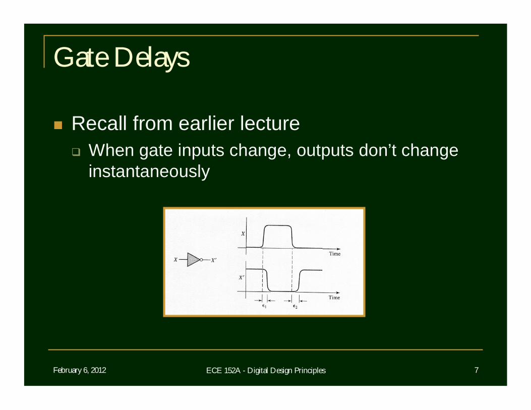
Gate Delays
Recall from earlier lecture When gate inputs change, outputs don’t change
instantaneously

February 6, 2012 ECE 152A - Digital Design Principles 8
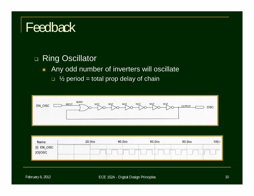
Feedback
Outputs connected to inputs Single inverter feedback
If propagation delay is long enough, output will oscillate

February 6, 2012 ECE 152A - Digital Design Principles 9
Feedback
If the propagation delay is not long enough, the output will settle somewhere in the middle Vin = Vout
February 6, 2012 ECE 152A - Digital Design Principles 10
Feedback
Ring Oscillator Any odd number of inverters will oscillate
½ period = total prop delay of chain

February 6, 2012 ECE 152A - Digital Design Principles 11
Feedback
What about an even number of inversions? Two inverter feedback
Memory (or State) Static 1 or 0 “stored” in memory

February 6, 2012 ECE 152A - Digital Design Principles 12
The Latch
Replace inverters with NOR gates
February 6, 2012 ECE 152A - Digital Design Principles 13
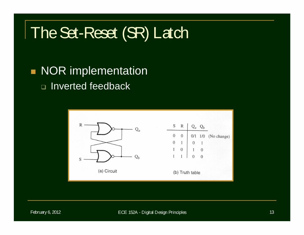
The Set-Reset (SR) Latch
NOR implementation Inverted feedback

February 6, 2012 ECE 152A - Digital Design Principles 14
The SR Latch
R = Reset (clear) Q → 0, Q* → 1
S = Set (preset) Q → 1, Q* → 0
NOR gate implementation Either input = 1 forces an output to 0

February 6, 2012 ECE 152A - Digital Design Principles 15
The SR Latch (cont)
Terminology Present state, Q
Current value of Q and Q* Next state, Q+
Final value of Q and Q* after input changes

February 6, 2012 ECE 152A - Digital Design Principles 16
The SR Latch (cont)
Operation S=1, R=0 : set to 1, Q+ = 1 S=0, R=1 : reset to 0, Q+ = 0 S=0, R=0 : hold state, Q+ = Q S=1, R=1 : not allowed
Q+ = Q*+ = 0, lose state
February 6, 2012 ECE 152A - Digital Design Principles 17
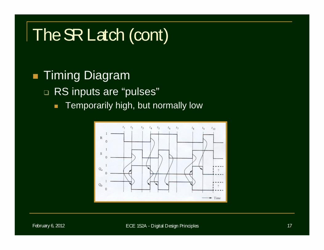
The SR Latch (cont)
Timing Diagram RS inputs are “pulses”
Temporarily high, but normally low
February 6, 2012 ECE 152A - Digital Design Principles 18
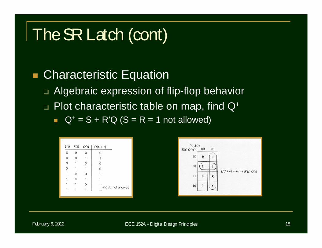
The SR Latch (cont)
Characteristic Equation Algebraic expression of flip-flop behavior Plot characteristic table on map, find Q+
Q+ = S + R’Q (S = R = 1 not allowed)
February 6, 2012 ECE 152A - Digital Design Principles 19
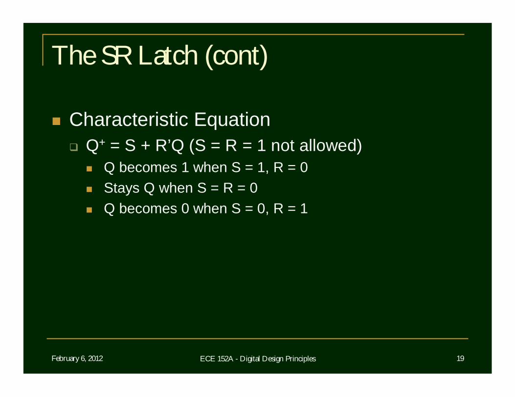
The SR Latch (cont)
Characteristic Equation Q+ = S + R’Q (S = R = 1 not allowed)
Q becomes 1 when S = 1, R = 0 Stays Q when S = R = 0 Q becomes 0 when S = 0, R = 1
February 6, 2012 ECE 152A - Digital Design Principles 20
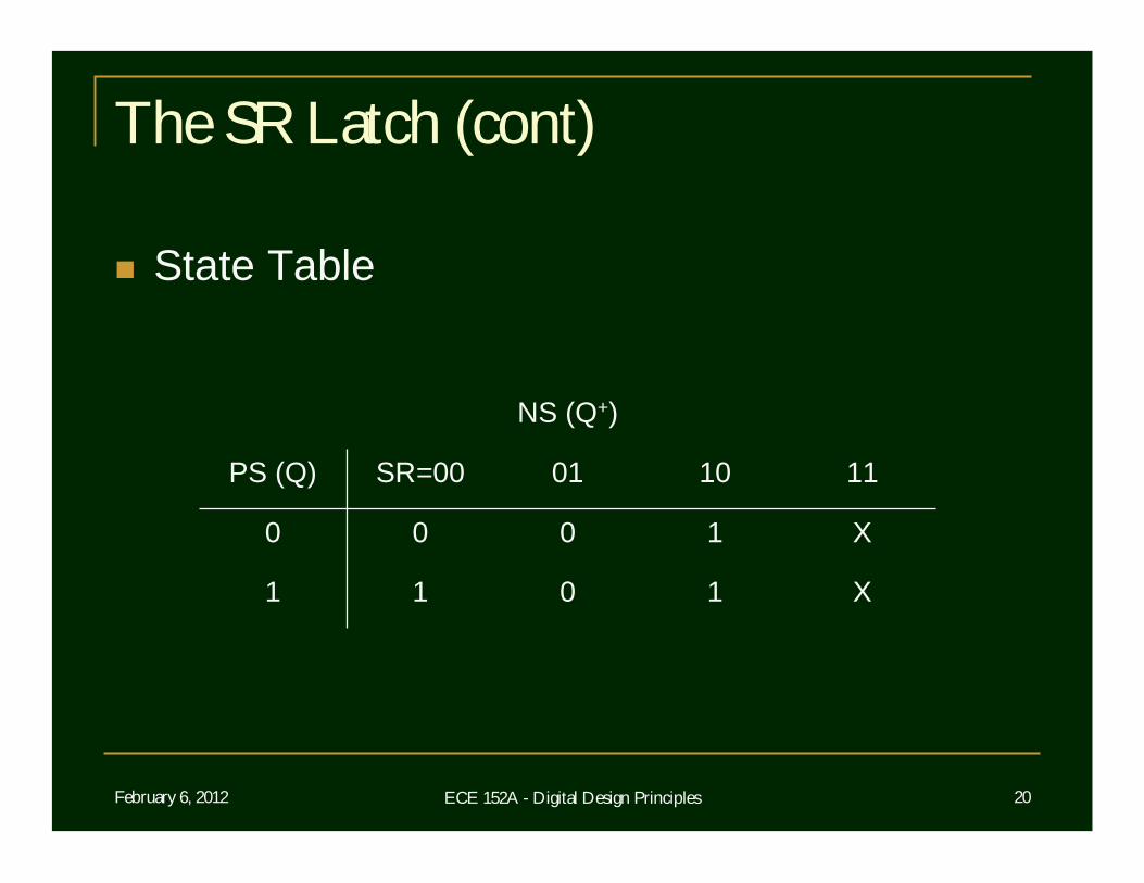
The SR Latch (cont)
State Table
1
1
10
X011
X000
1101SR=00PS (Q)
NS (Q+)

February 6, 2012 ECE 152A - Digital Design Principles 21
The SR Latch (cont)
State Diagram
1 0
SR = 01
SR = 10
SR = 0XSR = X0

February 6, 2012 ECE 152A - Digital Design Principles 22
The SR Latch with NANDS
NAND Based S’R’ Latch S’ = R’ = 0 not allowed Either input = 0 forces output to 1

February 6, 2012 ECE 152A - Digital Design Principles 23
The Gated SR Latch
Also known as “transparent” latch Output follows input (transparent) when enabled

February 6, 2012 ECE 152A - Digital Design Principles 24
The Gated SR Latch (cont)
Timing Diagram

February 6, 2012 ECE 152A - Digital Design Principles 25
The Gated SR Latch (cont)
NAND Implementation
February 6, 2012 ECE 152A - Digital Design Principles 26
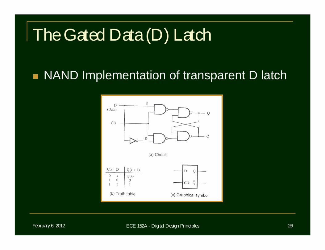
The Gated Data (D) Latch
NAND Implementation of transparent D latch

February 6, 2012 ECE 152A - Digital Design Principles 27
The Gated D Latch
Timing Diagram

February 6, 2012 ECE 152A - Digital Design Principles 28
The Edge Triggered D Flip-Flop
The D Flip-Flop Input D, latched and passed to Q on clock edge Rising edge triggered or falling edge triggered
Characteristic table and function
February 6, 2012 ECE 152A - Digital Design Principles 29
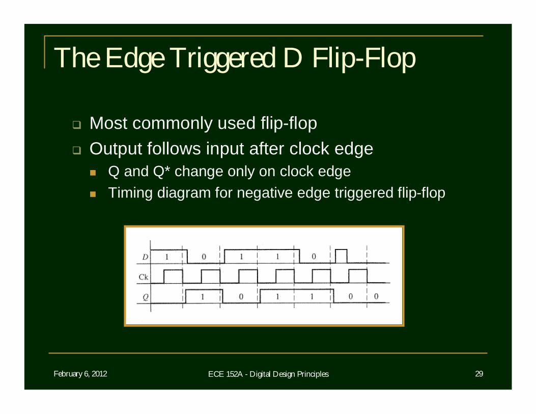
The Edge Triggered D Flip-Flop
Most commonly used flip-flop Output follows input after clock edge
Q and Q* change only on clock edge Timing diagram for negative edge triggered flip-flop

February 6, 2012 ECE 152A - Digital Design Principles 30
The D Flip-Flop
State Table
101
100
D = 1D = 0PS (Q)
NS (Q+)

February 6, 2012 ECE 152A - Digital Design Principles 31
The D Flip-Flop (cont)
State Diagram
1 0
D = 0
D = 1
D = 0D = 1

February 6, 2012 ECE 152A - Digital Design Principles 32
The Master-Slave D Flip-Flop
Construct edge triggered flip-flop from 2 transparent latches Many other topologies for edge triggered flip-flops Falling edge triggered (below)

February 6, 2012 ECE 152A - Digital Design Principles 33
The Master-Slave D Flip-Flop (cont)
Timing Diagram Falling edge triggered
February 6, 2012 ECE 152A - Digital Design Principles 34
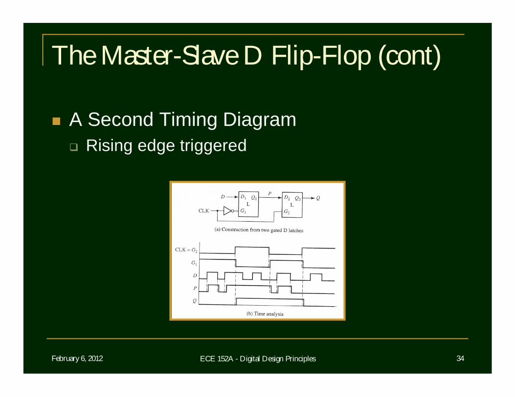
The Master-Slave D Flip-Flop (cont)
A Second Timing Diagram Rising edge triggered
February 6, 2012 ECE 152A - Digital Design Principles 35
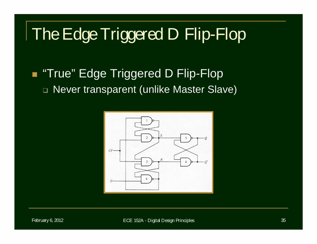
The Edge Triggered D Flip-Flop
“True” Edge Triggered D Flip-Flop Never transparent (unlike Master Slave)
February 6, 2012 ECE 152A - Digital Design Principles 36
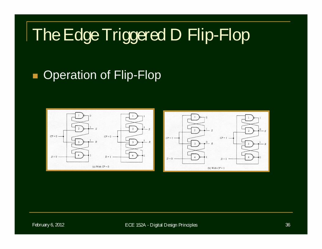
The Edge Triggered D Flip-Flop
Operation of Flip-Flop

February 6, 2012 ECE 152A - Digital Design Principles 37
Types of D Flip-Flops
Gated, Positive Edge and Negative Edge

February 6, 2012 ECE 152A - Digital Design Principles 38
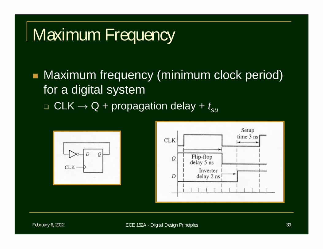
Timing Parameters
CLK → Q Delay from clock edge (CLK) to valid (Q, Q*) output
Setup time tsu Stable, valid data (D) before clock edge (CLK)
Hold time thold Stable, valid data (D) after clock edge (CLK)
February 6, 2012 ECE 152A - Digital Design Principles 39
Maximum Frequency
Maximum frequency (minimum clock period) for a digital system CLK → Q + propagation delay + tsu

February 6, 2012 ECE 152A - Digital Design Principles 40
Counter Design with D Flip-Flops
Design Example #1: Modulo 3 counter 00 → 01 → 10 ↓
↑ ← ← ←←← Requires 2 flip-flops One for each “state variable”

February 6, 2012 ECE 152A - Digital Design Principles 41
Counter Design with D Flip-Flops
State Diagram
00 01
10Transitions onclock edge

February 6, 2012 ECE 152A - Digital Design Principles 42
Counter Design with D Flip-Flops
State Table
XX11000101101000B+A+BA
NSPS

February 6, 2012 ECE 152A - Digital Design Principles 43
Counter Design with D Flip-Flops
Next State Maps
0
1
0 1
0 1
0 X
AB
0
1
0 1A
B
0
01
X
A+ = B B+ = A’B’
February 6, 2012 ECE 152A - Digital Design Principles 44
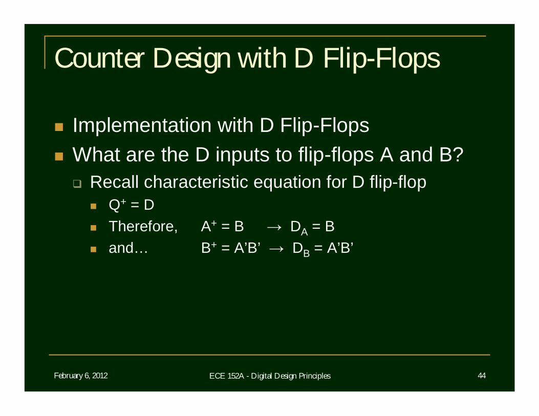
Counter Design with D Flip-Flops
Implementation with D Flip-Flops What are the D inputs to flip-flops A and B? Recall characteristic equation for D flip-flop
Q+ = D Therefore, A+ = B → DA = B and… B+ = A’B’ → DB = A’B’

February 6, 2012 ECE 152A - Digital Design Principles 45
Counter Design with D Flip-Flops
Implementation with positive edge triggered flip-flops

February 6, 2012 ECE 152A - Digital Design Principles 46
Counter Design with D Flip-Flops
Implementation with positive edge triggered flip-flops Timing diagram
00 01 10 00 01

February 6, 2012 ECE 152A - Digital Design Principles 47
Counter Design with D Flip-Flops
Design Example #2: Modulo 3 counter with up/down* input
Counter counts up with input = 1 and down with input = 0
Implement with D flip-flops

February 6, 2012 ECE 152A - Digital Design Principles 48
Counter Design with D Flip-Flops
State diagram
00 01
10
0
0
0 1
1
1

February 6, 2012 ECE 152A - Digital Design Principles 49
Counter Design with D Flip-Flops
State table
XX111000110110110001XX1101001000100
01000B+A+BAU

February 6, 2012 ECE 152A - Digital Design Principles 50
Counter Design with D Flip-Flops
Next state maps and flip-flop inputs
AB
U00 01
0
1
11 10
1
1
X
X
AB
U00 01
0
1
11 10
1 X
1X
A+ = DA = UB + U’A’B’ B+ = DB = U’A + UA’B’