Ja-Yol Lee and Hyun-Kyu Yu 52-GHz Millimetre-Wave PLL Synthesizer
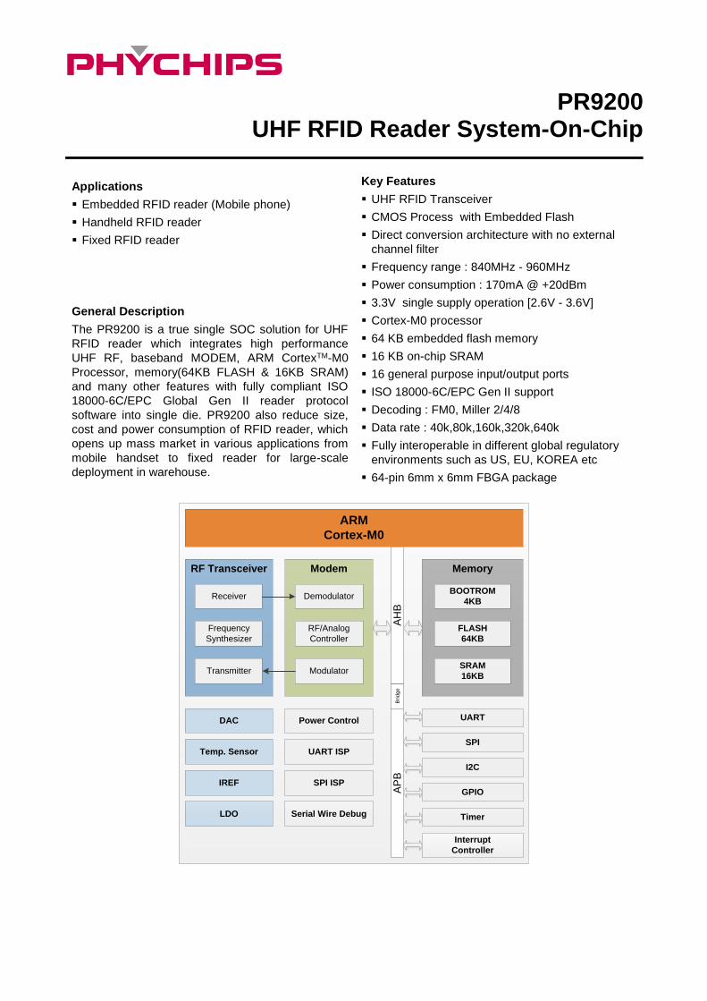
PR9200
UHF RFID Reader System-On-Chip
Applications
Embedded RFID reader (Mobile phone)
Handheld RFID reader
Fixed RFID reader
General Description
The PR9200 is a true single SOC solution for UHF
RFID reader which integrates high performance
UHF RF, baseband MODEM, ARM CortexTM-M0
Processor, memory(64KB FLASH & 16KB SRAM)
and many other features with fully compliant ISO
18000-6C/EPC Global Gen II reader protocol
software into single die. PR9200 also reduce size,
cost and power consumption of RFID reader, which
opens up mass market in various applications from
mobile handset to fixed reader for large-scale
deployment in warehouse.
Key Features
UHF RFID Transceiver
CMOS Process with Embedded Flash
Direct conversion architecture with no external
channel filter
Frequency range : 840MHz - 960MHz
Power consumption : 170mA @ +20dBm
3.3V single supply operation [2.6V - 3.6V]
Cortex-M0 processor
64 KB embedded flash memory
16 KB on-chip SRAM
16 general purpose input/output ports
ISO 18000-6C/EPC Gen II support
Decoding : FM0, Miller 2/4/8
Data rate : 40k,80k,160k,320k,640k
Fully interoperable in different global regulatory
environments such as US, EU, KOREA etc
64-pin 6mm x 6mm FBGA package
ARM
Cortex-M0
RF Transceiver Modem
RF/Analog
Controller
Modulator
DemodulatorReceiver
Transmitter
Frequency
Synthesizer
Memory
FLASH
64KB
BOOTROM
4KB
SRAM
16KB
SPI
I2C
Timer
UART ISP
Power ControlDAC
GPIO
Interrupt
Controller
Brid
ge
AH
BA
PB
Temp. Sensor
LDO
SPI ISP
Serial Wire Debug
UART
IREF
2
PR9200 Datasheet PR9200-LD013
Contents 1 Revision History ................................................................................................................................ 3 2 Electrical Characteristics ................................................................................................................. 4 2.1 Absolute Maximum Ratings ................................................................................................................ 4 2.2 Recommended Operating Conditions ................................................................................................. 4 2.3 Current Consumption (TBD) ............................................................................................................... 4 2.4 Radio Receiver Specifications (TBD) .................................................................................................. 5 2.5 Radio Transmitter Specifications (TBD) .............................................................................................. 5 2.6 Radio Frequency Synthesizer Specifications (TBD) ........................................................................... 6 3 Pin Description .................................................................................................................................. 7 4 Functional Block Description ........................................................................................................ 10 4.1 MCU .................................................................................................................................................. 11 4.2 MODEM ............................................................................................................................................. 13 4.3 RF ...................................................................................................................................................... 16 5 SYSTEM CONTROL ......................................................................................................................... 18 5.1 Operation mode control ..................................................................................................................... 18 5.2 Power up timing ................................................................................................................................. 20 5.3 ISP mode control ............................................................................................................................... 21 6 Software ........................................................................................................................................... 23 7 Application Schematic .................................................................................................................... 24 7.1 Antenna configuration ....................................................................................................................... 26 7.2 Power supply ..................................................................................................................................... 26 7.3 Internal LDOs .................................................................................................................................... 26 7.4 Rx input matching circuit ................................................................................................................... 26 7.5 Tx output matching circuit ................................................................................................................. 27 7.6 Oscillator ........................................................................................................................................... 27 8 Package Information ....................................................................................................................... 28 9 Address Information ....................................................................................................................... 29
3
PR9200 Datasheet PR9200-LD013
1 Revision History
Version Date Description
LD01 2012.7.12 preliminary
LD012 2012.7.16 Fixed pin description
LP mode -> Internal PA mode , HP mode -> External PA mode
LD013 2015.3.6 Fixed typo error
4
PR9200 Datasheet PR9200-LD013
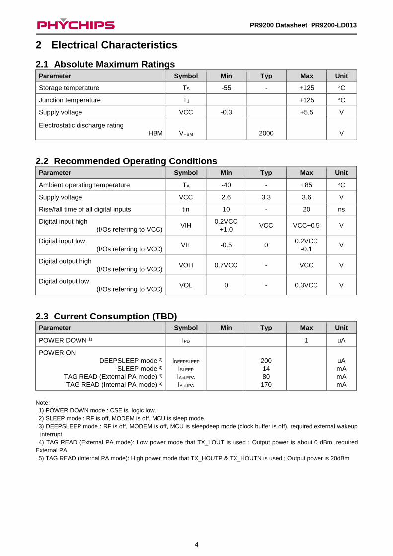
2 Electrical Characteristics
2.1 Absolute Maximum Ratings Parameter Symbol Min Typ Max Unit
Storage temperature TS -55 - +125 C
Junction temperature TJ +125 C
Supply voltage VCC -0.3 +5.5 V
Electrostatic discharge rating
HBM
VHBM
2000
V
2.2 Recommended Operating Conditions Parameter Symbol Min Typ Max Unit
Ambient operating temperature TA -40 - +85 C
Supply voltage VCC 2.6 3.3 3.6 V
Rise/fall time of all digital inputs tin 10 - 20 ns
Digital input high
(I/Os referring to VCC) VIH
0.2VCC
+1.0 VCC VCC+0.5 V
Digital input low
(I/Os referring to VCC) VIL -0.5 0
0.2VCC
-0.1 V
Digital output high
(I/Os referring to VCC) VOH 0.7VCC - VCC V
Digital output low
(I/Os referring to VCC) VOL 0 - 0.3VCC V
2.3 Current Consumption (TBD) Parameter Symbol Min Typ Max Unit
POWER DOWN 1) IPD 1 uA
POWER ON
DEEPSLEEP mode 2)
SLEEP mode 3)
TAG READ (External PA mode) 4)
TAG READ (Internal PA mode) 5)
IDEEPSLEEP
ISLEEP
IAct.EPA
IAct.IPA
200
14
80
170
uA
mA
mA
mA
Note:
1) POWER DOWN mode : CSE is logic low.
2) SLEEP mode : RF is off, MODEM is off, MCU is sleep mode.
3) DEEPSLEEP mode : RF is off, MODEM is off, MCU is sleepdeep mode (clock buffer is off), required external wakeup
interrupt
4) TAG READ (External PA mode): Low power mode that TX_LOUT is used ; Output power is about 0 dBm, required
External PA
5) TAG READ (Internal PA mode): High power mode that TX_HOUTP & TX_HOUTN is used ; Output power is 20dBm
5
PR9200 Datasheet PR9200-LD013
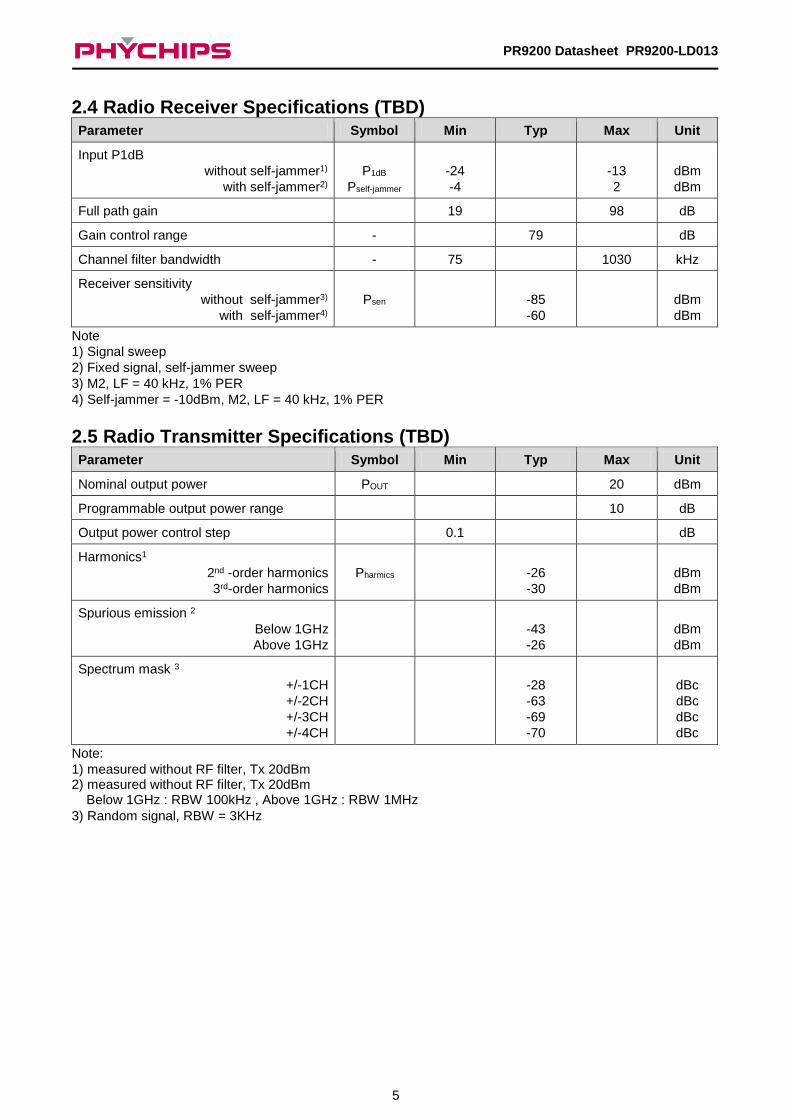
2.4 Radio Receiver Specifications (TBD) Parameter Symbol Min Typ Max Unit
Input P1dB
without self-jammer1)
with self-jammer2)
P1dB
Pself-jammer
-24
-4
-13
2
dBm
dBm
Full path gain 19 98 dB
Gain control range - 79 dB
Channel filter bandwidth - 75 1030 kHz
Receiver sensitivity
without self-jammer3)
with self-jammer4)
Psen
-85
-60
dBm
dBm
Note
1) Signal sweep
2) Fixed signal, self-jammer sweep
3) M2, LF = 40 kHz, 1% PER
4) Self-jammer = -10dBm, M2, LF = 40 kHz, 1% PER
2.5 Radio Transmitter Specifications (TBD) Parameter Symbol Min Typ Max Unit
Nominal output power POUT 20 dBm
Programmable output power range 10 dB
Output power control step 0.1 dB
Harmonics1
2nd -order harmonics
3rd-order harmonics
Pharmics
-26
-30
dBm
dBm
Spurious emission 2
Below 1GHz
Above 1GHz
-43
-26
dBm
dBm
Spectrum mask 3
+/-1CH
+/-2CH
+/-3CH
+/-4CH
-28
-63
-69
-70
dBc
dBc
dBc
dBc
Note:
1) measured without RF filter, Tx 20dBm 2) measured without RF filter, Tx 20dBm Below 1GHz : RBW 100kHz , Above 1GHz : RBW 1MHz
3) Random signal, RBW = 3KHz
6
PR9200 Datasheet PR9200-LD013
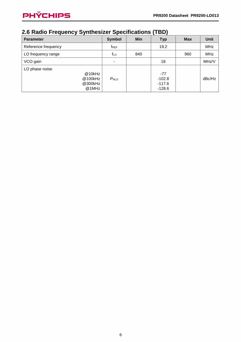
2.6 Radio Frequency Synthesizer Specifications (TBD) Parameter Symbol Min Typ Max Unit
Reference frequency fREF 19.2 MHz
LO frequency range fLO 840 960 MHz
VCO gain - 18 MHz/V
LO phase noise
@10kHz
@100kHz
@300kHz
@1MHz
PNLO
-77
-102.8
-117.6
-128.6
dBc/Hz
7
PR9200 Datasheet PR9200-LD013
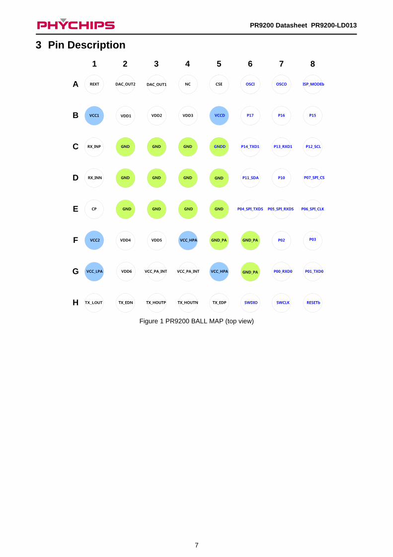
3 Pin Description
VCC1 VDD2 VDD3VDD1
GNDRX_INP
RX_INN
GNDGND
GND
VCC2
GNDGND
VDD4
CP GND GND
GND
VDD5
VCC_LPA GND_PA
GND_PA
VCC_PA_INT VCC_PA_INT
GND_PA
VCC_HPA
GNDD
VCCD
P00_RXD0 P01_TXD0
P02 P03
P04_SPI_TXDS P06_SPI_CLKP05_SPI_RXDS
P07_SPI_CS
P12_SCL
P11_SDA
P13_RXD1
P10
P15
P14_TXD1
P17 P16
ISP_MODEbOSCOOSCICSENCDAC_OUT1DAC_OUT2REXT
GND
VCC_HPA
GND
A
B
C
D
E
F
G
1 2 3 4 5 6 7 8
TX_HOUTPTX_EDN TX_HOUTN TX_EDP SWDIO SWCLK RESETbTX_LOUTH
VDD6
Figure 1 PR9200 BALL MAP (top view)
8
PR9200 Datasheet PR9200-LD013
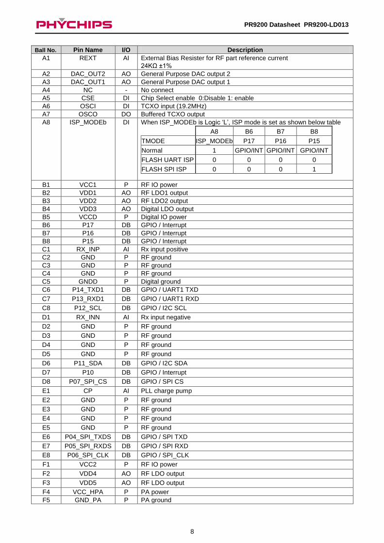
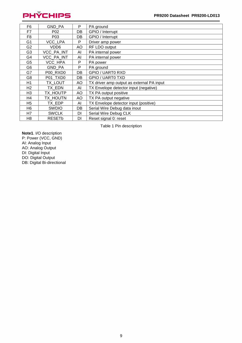
Ball No. Pin Name I/O Description
A1 REXT AI External Bias Resister for RF part reference current
24KΩ ±1%
A2 DAC_OUT2 AO General Purpose DAC output 2
A3 DAC_OUT1 AO General Purpose DAC output 1
A4 NC - No connect
A5 CSE DI Chip Select enable 0:Disable 1: enable
A6 OSCI DI TCXO input (19.2MHz)
A7 OSCO DO Buffered TCXO output
A8 ISP_MODEb DI When ISP_MODEb is Logic ‘L’, ISP mode is set as shown below table
A8 B6 B7 B8
TMODE ISP_MODEb P17 P16 P15
Normal 1 GPIO/INT GPIO/INT GPIO/INT
FLASH UART ISP 0 0 0 0
FLASH SPI ISP 0 0 0 1
B1 VCC1 P RF IO power
B2 VDD1 AO RF LDO1 output
B3 VDD2 AO RF LDO2 output
B4 VDD3 AO Digital LDO output
B5 VCCD P Digital IO power
B6 P17 DB GPIO / Interrupt
B7 P16 DB GPIO / Interrupt
B8 P15 DB GPIO / Interrupt
C1 RX_INP AI Rx input positive
C2 GND P RF ground
C3 GND P RF ground
C4 GND P RF ground
C5 GNDD P Digital ground
C6 P14_TXD1 DB GPIO / UART1 TXD
C7 P13_RXD1 DB GPIO / UART1 RXD
C8 P12_SCL DB GPIO / I2C SCL
D1 RX_INN AI Rx input negative
D2 GND P RF ground
D3 GND P RF ground
D4 GND P RF ground
D5 GND P RF ground
D6 P11_SDA DB GPIO / I2C SDA
D7 P10 DB GPIO / Interrupt
D8 P07_SPI_CS DB GPIO / SPI CS
E1 CP AI PLL charge pump
E2 GND P RF ground
E3 GND P RF ground
E4 GND P RF ground
E5 GND P RF ground
E6 P04_SPI_TXDS DB GPIO / SPI TXD
E7 P05_SPI_RXDS DB GPIO / SPI RXD
E8 P06_SPI_CLK DB GPIO / SPI_CLK
F1 VCC2 P RF IO power
F2 VDD4 AO RF LDO output
F3 VDD5 AO RF LDO output
F4 VCC_HPA P PA power
F5 GND_PA P PA ground
9
PR9200 Datasheet PR9200-LD013
F6 GND_PA P PA ground
F7 P02 DB GPIO / Interrupt
F8 P03 DB GPIO / Interrupt
G1 VCC_LPA P Driver amp power
G2 VDD6 AO RF LDO output
G3 VCC_PA_INT AI PA internal power
G4 VCC_PA_INT AI PA internal power
G5 VCC_HPA P PA power
G6 GND_PA P PA ground
G7 P00_RXD0 DB GPIO / UART0 RXD
G8 P01_TXD0 DB GPIO / UART0 TXD
H1 TX_LOUT AO TX driver amp output as external PA input
H2 TX_EDN AI TX Envelope detector input (negative)
H3 TX_HOUTP AO TX PA output positive
H4 TX_HOUTN AO TX PA output negative
H5 TX_EDP AI TX Envelope detector input (positive)
H6 SWDIO DB Serial Wire Debug data inout
H7 SWCLK DI Serial Wire Debug CLK
H8 RESETb DI Reset signal 0: reset
Table 1 Pin description
Note1. I/O description
P: Power (VCC, GND)
AI: Analog Input
AO: Analog Output
DI: Digital Input
DO: Digital Output
DB: Digital Bi-directional
10
PR9200 Datasheet PR9200-LD013
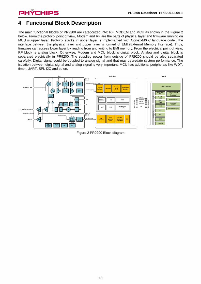
4 Functional Block Description
The main functional blocks of PR9200 are categorized into: RF, MODEM and MCU as shown in the Figure 2
below. From the protocol point of view, Modem and RF are the parts of physical layer and firmware running on
MCU is upper layer. Protocol stacks in upper layer is implemented with Cortex-M0 C language code. The
interface between the physical layer and upper layer is formed of EMI (External Memory Interface). Thus,
firmware can access lower layer by reading from and writing to EMI memory. From the electrical point of view,
RF block is analog block. Otherwise, Modem and MCU block is digital block. Analog and digital block is
separated electrically in PR9200. The supplied power from outside of PR9200 should be also separated
carefully. Digital signal could be coupled to analog signal and that may depredate system performance. The
isolation between digital signal and analog signal is very important. MCU has additional peripherals like WDT,
timer, UART, SPI, I2C and so on.
6-bitADC
6-bitADC
Gain ctrl
BW ctrl
Polarity control
Amplitude control
PA
12-bitDAC
4th LPF
TX DATA<11:0>
PHASE_Ctrl
BW ctrl
LOBUF
÷2
÷2÷2
CLK
PFD/CP
CP÷4/5 PS
P
S
÷R
LF
6-bitGP DAC[Dual]
TEMPSENSOR
LDO IREF
PHASETrim.
LNB
LNB PGA
PGA
DA
ADC_DATA_I[5:0]
ADC_DATA_Q[5:0]
DCOC ctrl
AGC
Signal Detector
Pre-distortion
DSB-ASKWaveform
Lookuptable
CorrelatorTiming error
Detection
RF Register controller E
MI In
terf
ace
Gain Ctrl
Inter-polation
Filter
RX
TX
RF control
RSSI
DSM EM
I In
terf
ace
ARM Cortex-M0
Test modecontrol
EMI_CLK
EMI_ADDR
EMI_DIN
EMI_DOUT
INT
Power control
UART & SPI ISP[Firmware download]
UART
SPI
I2C
FLASH64KB
BOOTROM4KB
SRAM16KB
GPIO
Timer0,1
AH
BA
HB
2A
PB
Interrupt controller
RF MODEM MCU
FM0/MillerDecoder
PIE
AFC
RX INP/RX_INN
TX HOUTP/TXHOUTN
TX LOUT
TX_EDP/TX_EDN
Figure 2 PR9200 Block diagram
11
PR9200 Datasheet PR9200-LD013
4.1 MCU
PR9200 includes ARM Cortex-M0 based, low cost 32-bit MCU, low power, simple instruction set and memory
addressing together with reduced code size compared to existing 8bit architectures. PR9200 operate
19.2MHz main clock. Also it includes 64KB embedded flash memory, 16kB DATA SRAM, 4KB Boot ROM, two
UART, fast I2C, SSP, GPIO, two dual input timers, WDT, software debugging interface.
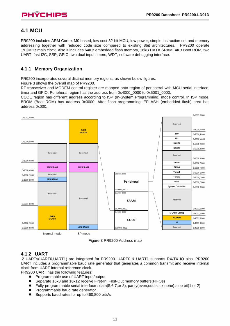
4.1.1 Memory Organization
PR9200 incorporates several distinct memory regions, as shown below figures.
Figure 3 shows the overall map of PR9200.
RF transceiver and MODEM control register are mapped onto region of peripheral with MCU serial interface,
timer and GPIO. Peripheral region has the address from 0x4000_0000 to 0x5001_0000.
CODE region has different address according to ISP (In-System Programming) mode control. In ISP mode,
BROM (Boot ROM) has address 0x0000. After flash programming, EFLASH (embedded flash) area has
address 0x000.
0x0000_0000
CODE
0x1FFF_FFFF
0x2000_0000
SRAM
0x3FFF_FFFF
0x4000_0000
Peripheral
0x5FFF_FFFF
Reserved 0x4000_0000
MODEM
0x4001_0000RF
0x4001_8000
EFLASH Config 0x4002_0000
Reserved
0x4003_0000
0x5000_0000System Controller
0x5000_1000WDT
0x5000_2000Timer0
0x5000_3000Timer1
0x5000_4000GPIO0
0x5000_5000GPIO1
0x5000_6000
Reserved
0x5000_8000UART0
0x5000_9000UART1
0x5000_A000I2C
Reserved
0x5000_C000
0x5001_0000
4KB BROM
Reserved
Reserved
64KBEFLASH
0x0000_0000
0x0001_0000
Normal mode ISP mode
Reserved
0x1000_0000 4KB BROM
0x1000_1000 Reserved
16KB IRAM
0x1000_4000
0x1000_8000
Reserved
0x2000_0000
0x0000_1000
16KB IRAM
64KBEFLASH
0x2001_0000
0x5000_B000SSP
Figure 3 PR9200 Address map
4.1.2 UART 2 UARTs(UART0,UART1) are integrated for PR9200. UART0 & UART1 supports RX/TX IO pins. PR9200 UART includes a programmable baud rate generator that generates a common transmit and receive internal clock from UART internal reference clock. PR9200 UART has the following features:
Programmable use of UART input/output. Separate 16x8 and 16x12 receive First-In, First-Out memory buffers(FIFOs) Fully-programmable serial interface : data(5,6,7,or 8), parity(even,odd,stick,none),stop bit(1 or 2) Programmable baud rate generator Supports baud rates for up to 460,800 bits/s
12
PR9200 Datasheet PR9200-LD013
4.1.3 SSP PR9200 SSP is a master or slave interface for SPI synchronous serial communication with peripheral devices It performs serial-to-parallel conversion on data received from a peripheral device. PR9200 SSP has the following features:
Master / slave operation Programmable clock bit rate Programmable choice of LSB first or MSB first data frame Programmable data frame size from 4 to 16 bits Independent masking of transmit FIFO, receive FIFO Master mode 9.6MHz (Max) Slave mode 3MHz (Max)
4.1.4 I2C I2C is a multi-master I2C bus module. Only two lines are required; data (SDA) and clock (SCL) PR9200 I2C has the following features:
Serial, 8-bit oriented, bi-directional data transfers Up to 100kbit/s in the standard mode Up to 300kbit/s in the Fast mode Multi-master I2C-bus including collision detection and arbiration
4.1.5 WDT PR9200 WDT( Watch Dog Timer) module is based around a 32-bit down counter that is initialized from Reload register. WDT is intended to be used to apply a reset to a system in the event of a software failure, providing a way of recovering from software crashes.
4.1.6 Timer Dual input timer (timer0, timer1) module consists of two programmable 32/16-bit down counters that can generate interrupts on reaching zero. It has three timer modes: free-running, periodic, one-shot.
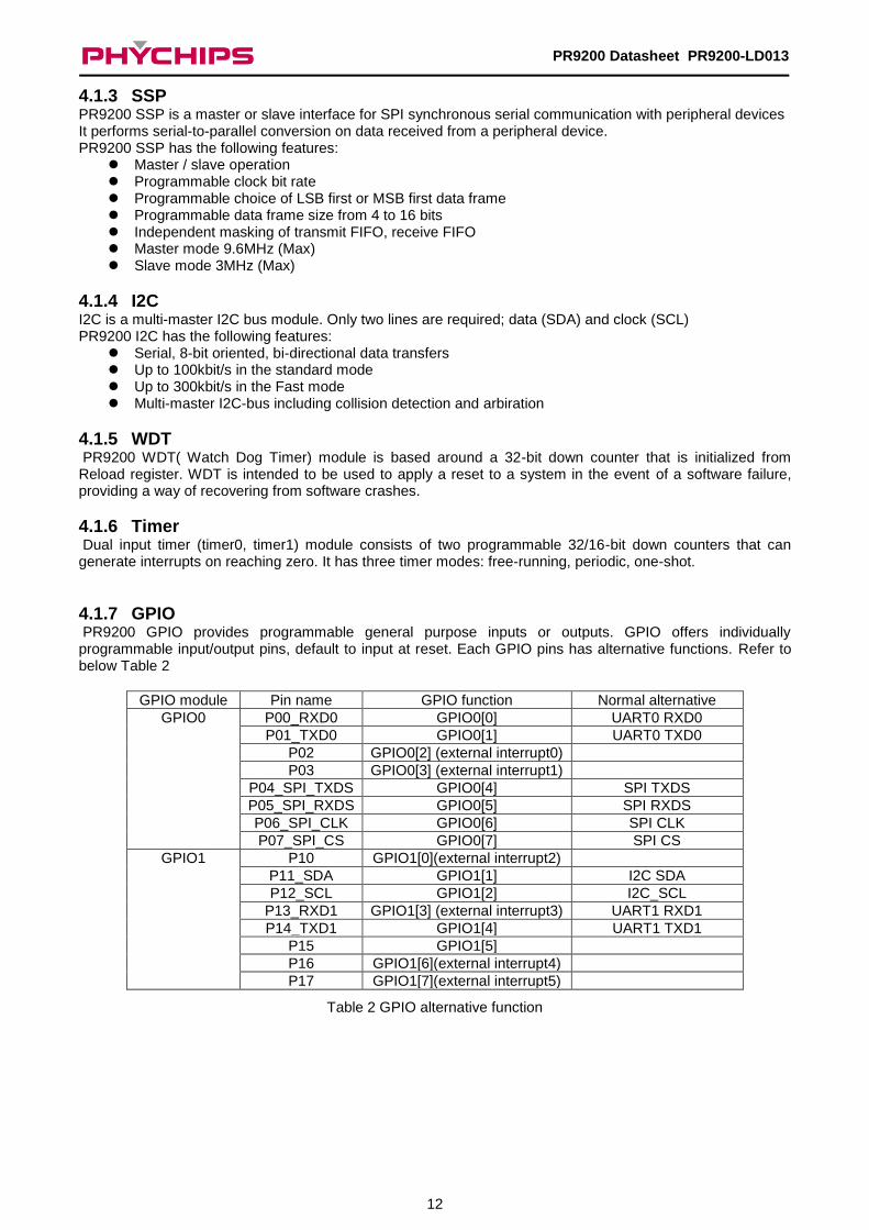
4.1.7 GPIO PR9200 GPIO provides programmable general purpose inputs or outputs. GPIO offers individually programmable input/output pins, default to input at reset. Each GPIO pins has alternative functions. Refer to below Table 2
GPIO module Pin name GPIO function Normal alternative
GPIO0 P00_RXD0 GPIO0[0] UART0 RXD0
P01_TXD0 GPIO0[1] UART0 TXD0
P02 GPIO0[2] (external interrupt0)
P03 GPIO0[3] (external interrupt1)
P04_SPI_TXDS GPIO0[4] SPI TXDS
P05_SPI_RXDS GPIO0[5] SPI RXDS
P06_SPI_CLK GPIO0[6] SPI CLK
P07_SPI_CS GPIO0[7] SPI CS
GPIO1 P10 GPIO1[0](external interrupt2)
P11_SDA GPIO1[1] I2C SDA
P12_SCL GPIO1[2] I2C_SCL
P13_RXD1 GPIO1[3] (external interrupt3) UART1 RXD1
P14_TXD1 GPIO1[4] UART1 TXD1
P15 GPIO1[5]
P16 GPIO1[6](external interrupt4)
P17 GPIO1[7](external interrupt5)
Table 2 GPIO alternative function
13
PR9200 Datasheet PR9200-LD013
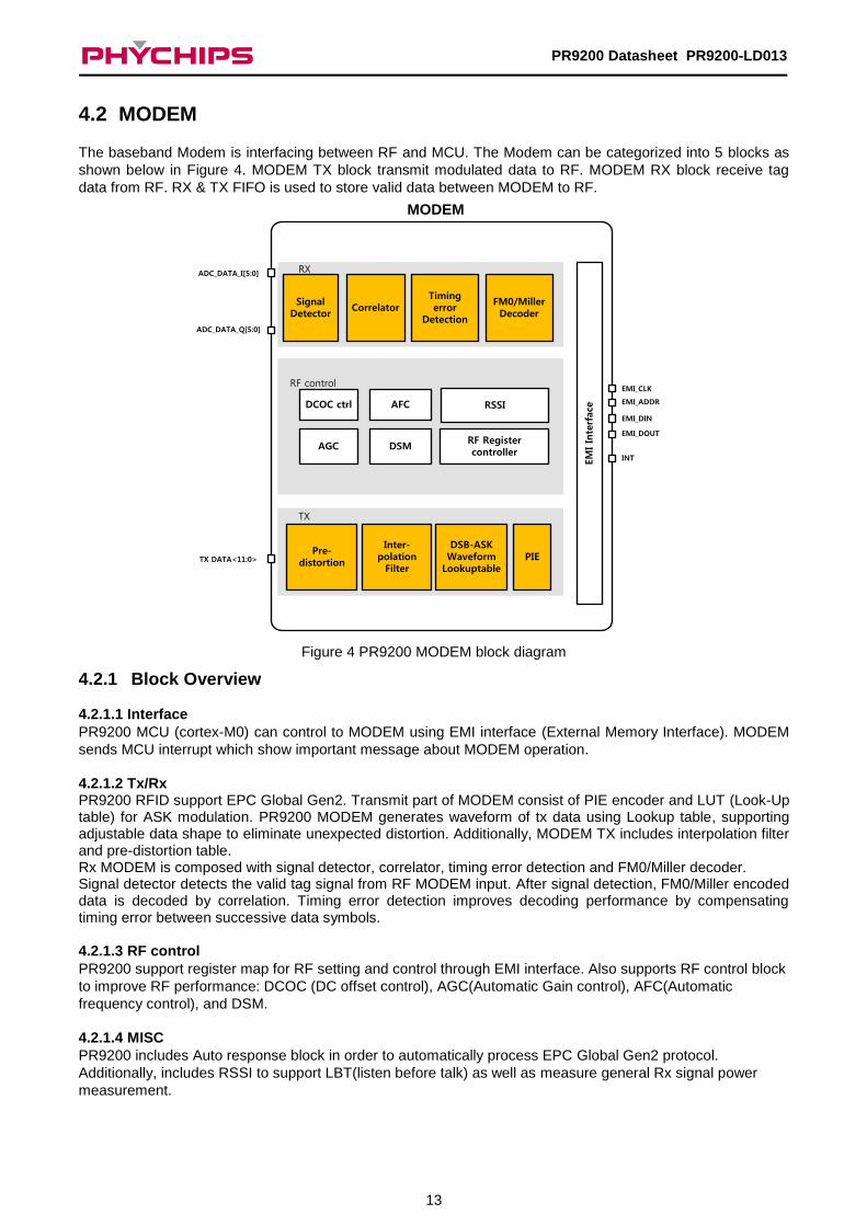
4.2 MODEM
The baseband Modem is interfacing between RF and MCU. The Modem can be categorized into 5 blocks as
shown below in Figure 4. MODEM TX block transmit modulated data to RF. MODEM RX block receive tag
data from RF. RX & TX FIFO is used to store valid data between MODEM to RF.
DCOC ctrl
AGC
Signal Detector
Pre-distortion
DSB-ASKWaveform
Lookuptable
CorrelatorTiming error
Detection
RF Register controller
EM
I In
terf
ace
Inter-polation
Filter
RX
TX
RF control
RSSI
DSM
MODEM
FM0/MillerDecoder
PIE
AFC
TX DATA<11:0>
ADC_DATA_I[5:0]
ADC_DATA_Q[5:0]
EMI_CLK
EMI_ADDR
EMI_DIN
EMI_DOUT
INT
Figure 4 PR9200 MODEM block diagram
4.2.1 Block Overview 4.2.1.1 Interface
PR9200 MCU (cortex-M0) can control to MODEM using EMI interface (External Memory Interface). MODEM
sends MCU interrupt which show important message about MODEM operation.
4.2.1.2 Tx/Rx PR9200 RFID support EPC Global Gen2. Transmit part of MODEM consist of PIE encoder and LUT (Look-Up table) for ASK modulation. PR9200 MODEM generates waveform of tx data using Lookup table, supporting adjustable data shape to eliminate unexpected distortion. Additionally, MODEM TX includes interpolation filter and pre-distortion table. Rx MODEM is composed with signal detector, correlator, timing error detection and FM0/Miller decoder. Signal detector detects the valid tag signal from RF MODEM input. After signal detection, FM0/Miller encoded data is decoded by correlation. Timing error detection improves decoding performance by compensating timing error between successive data symbols.
4.2.1.3 RF control
PR9200 support register map for RF setting and control through EMI interface. Also supports RF control block
to improve RF performance: DCOC (DC offset control), AGC(Automatic Gain control), AFC(Automatic
frequency control), and DSM.
4.2.1.4 MISC
PR9200 includes Auto response block in order to automatically process EPC Global Gen2 protocol.
Additionally, includes RSSI to support LBT(listen before talk) as well as measure general Rx signal power
measurement.
14
PR9200 Datasheet PR9200-LD013
4.2.2 RX Modulator state machine
RXFIRSTTIMING
RXSIGNALSENSING
RXDATARECEIVE
RXSFDDETECTION
RXRECEIVEEND
(1)
(2)
(3)(4)
(5)
(6)
(7)
(8)
(9)(10)
RXIDLE
Figure 5 Rx Finite state machine diagram
Table 3
from to conditions
(1) RXIDLE RXSIGNALSENSING rx_enable
(2) RXSIGNALSENSING RXFIRSTTIMING rx_enable & rx_signal_detected_done
(3) RXFIRSTTIMING RXSFDDETECTION rx_enable & next_first_timing_est_done
(4) RXSFDDETECTION RXDATARECEIVE rx_enable & next_preamble_det
(5) RXDATARECEIVE RXRECEIVEEND rx_enable & next_receive_complete
(6) RXRECEIVEEND RXIDLE !rx_enable
(7) RXSIGNALSENSING RXIDLE !rx_enable
(8) RXFIRSTTIMING RXIDLE !rx_enable
(9) RXSFDDETECTION RXIDLE !rx_enable
(10) RXDATARECEIVE RXIDLE !rx_enable
4.2.2.1 RXIDLE state When rx_enable(modem internal signal) is low, PR9200 enter receive ready or receive stop state. Also all variable of digital modulator are initialized.
4.2.2.2 RXSIGNALSENSING state In RXSIGNALSENSING state, PR9200 wait Tag signal and determine whether input signal is valid signal or noise. 4.2.2.3 RXFIRSTTIMING state In RXFIRSTTIMING state, PR9200 take correlation about 1-LF period pulse signal and determine first frame-sync.
15
PR9200 Datasheet PR9200-LD013
4.2.2.4 RXSFDDETECTION state
PR9200 look for Predefined pattern in preamble called SFD (start Frame Detect) in RXSFDDETECTION state. If modulation method is FM0, expected pattern is “1010v1” . otherwise if modulation method is Miller, PR9200 extract “0101111”.
4.2.2.5 RXDATARECEIVE state In RXDATARECEIVE state, PR9200 demodulate a series of received data until the end of signal.
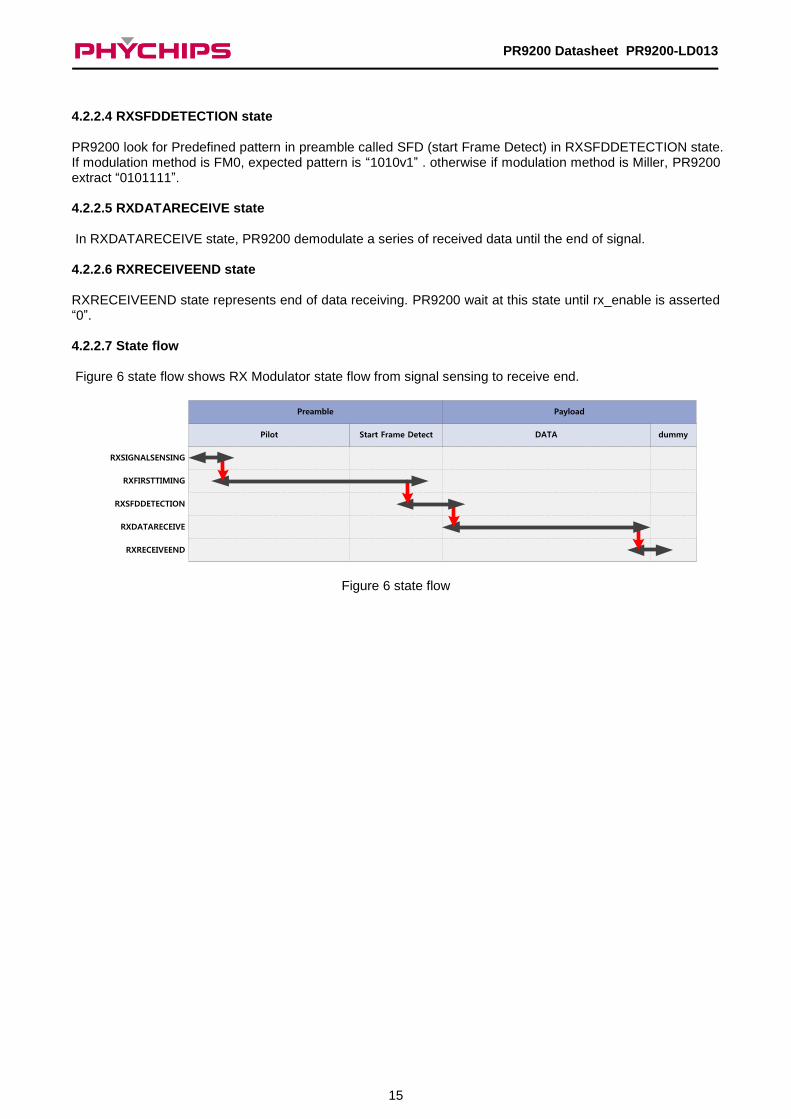
4.2.2.6 RXRECEIVEEND state RXRECEIVEEND state represents end of data receiving. PR9200 wait at this state until rx_enable is asserted “0”. 4.2.2.7 State flow Figure 6 state flow shows RX Modulator state flow from signal sensing to receive end.
Pilot Start Frame Detect DATA
Preamble Payload
dummy
RXSIGNALSENSING
RXFIRSTTIMING
RXDATARECEIVE
RXSFDDETECTION
RXRECEIVEEND
Figure 6 state flow
16
PR9200 Datasheet PR9200-LD013
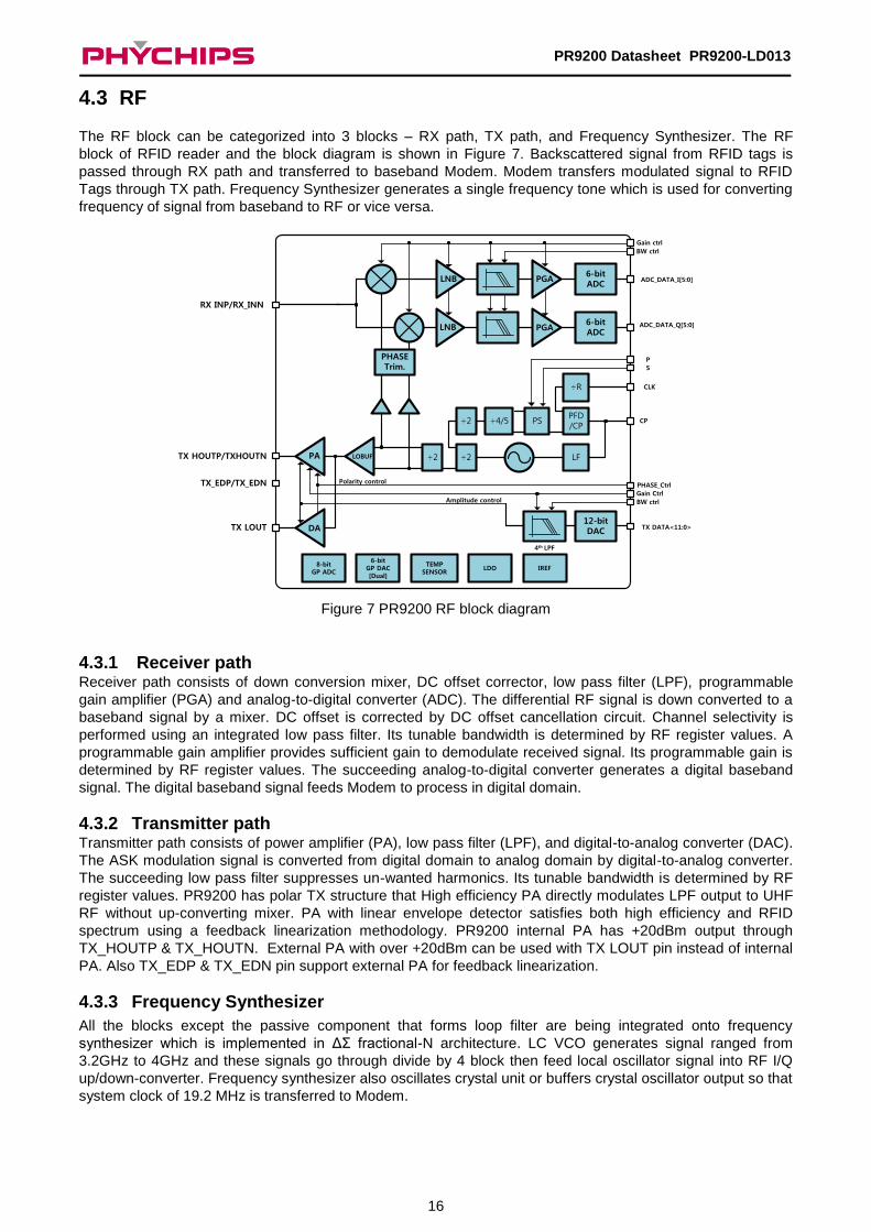
4.3 RF
The RF block can be categorized into 3 blocks – RX path, TX path, and Frequency Synthesizer. The RF
block of RFID reader and the block diagram is shown in Figure 7. Backscattered signal from RFID tags is
passed through RX path and transferred to baseband Modem. Modem transfers modulated signal to RFID
Tags through TX path. Frequency Synthesizer generates a single frequency tone which is used for converting
frequency of signal from baseband to RF or vice versa.
6-bitADC
6-bitADC
Gain ctrl
BW ctrl
Polarity control
Amplitude control
PA
12-bitDAC
4th LPF
PHASE_Ctrl
BW ctrl
LOBUF
÷2
÷2÷2
CLK
PFD/CP
CP÷4/5 PS
P
S
÷R
LF
RX INP/RX_INN
TX HOUTP/TXHOUTN
6-bitGP DAC[Dual]
TEMPSENSOR
LDO IREF
PHASETrim.
LNB
LNB PGA
PGA
TX LOUT DA
TX_EDP/TX_EDNGain Ctrl
8-bitGP ADC
ADC_DATA_I[5:0]
ADC_DATA_Q[5:0]
TX DATA<11:0>
Figure 7 PR9200 RF block diagram
4.3.1 Receiver path Receiver path consists of down conversion mixer, DC offset corrector, low pass filter (LPF), programmable
gain amplifier (PGA) and analog-to-digital converter (ADC). The differential RF signal is down converted to a
baseband signal by a mixer. DC offset is corrected by DC offset cancellation circuit. Channel selectivity is
performed using an integrated low pass filter. Its tunable bandwidth is determined by RF register values. A
programmable gain amplifier provides sufficient gain to demodulate received signal. Its programmable gain is
determined by RF register values. The succeeding analog-to-digital converter generates a digital baseband
signal. The digital baseband signal feeds Modem to process in digital domain.
4.3.2 Transmitter path Transmitter path consists of power amplifier (PA), low pass filter (LPF), and digital-to-analog converter (DAC).
The ASK modulation signal is converted from digital domain to analog domain by digital-to-analog converter.
The succeeding low pass filter suppresses un-wanted harmonics. Its tunable bandwidth is determined by RF
register values. PR9200 has polar TX structure that High efficiency PA directly modulates LPF output to UHF
RF without up-converting mixer. PA with linear envelope detector satisfies both high efficiency and RFID
spectrum using a feedback linearization methodology. PR9200 internal PA has +20dBm output through
TX_HOUTP & TX_HOUTN. External PA with over +20dBm can be used with TX LOUT pin instead of internal
PA. Also TX_EDP & TX_EDN pin support external PA for feedback linearization.
4.3.3 Frequency Synthesizer
All the blocks except the passive component that forms loop filter are being integrated onto frequency
synthesizer which is implemented in ΔΣ fractional-N architecture. LC VCO generates signal ranged from
3.2GHz to 4GHz and these signals go through divide by 4 block then feed local oscillator signal into RF I/Q
up/down-converter. Frequency synthesizer also oscillates crystal unit or buffers crystal oscillator output so that
system clock of 19.2 MHz is transferred to Modem.
17
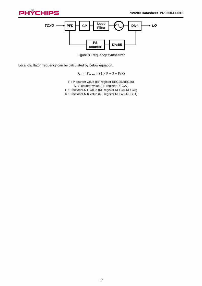
PR9200 Datasheet PR9200-LD013
PFD CPLoop
Filter
Div4/5PS
counter
Div4TCXO LO
Figure 8 Frequency synthesizer
Local oscillator frequency can be calculated by below equation.
FLO = FTCXO × (4 × P + S + F/K)
P : P counter value (RF register REG25,REG26)
S : S counter value (RF register REG27)
F : Fractional-N F value (RF register REG76-REG78)
K : Fractional-N K value (RF register REG79-REG81)
18
PR9200 Datasheet PR9200-LD013
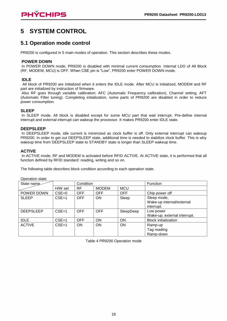
5 SYSTEM CONTROL
5.1 Operation mode control PR9200 is configured in 5 main modes of operation. This section describes these modes.
POWER DOWN In POWER DOWN mode, PR9200 is disabled with minimal current consumption. Internal LDO of All Block (RF, MODEM, MCU) is OFF. When CSE pin is “Low”, PR9200 enter POWER DOWN mode.
IDLE All block of PR9200 are initialized when it enters the IDLE mode. After MCU is initialized, MODEM and RF
part are initialized by instruction of firmware. Also RF goes through variable calibration: AFC (Automatic Frequency calibration), Channel setting, AFT (Automatic Filter tuning). Completing initialization, some parts of PR9200 are disabled in order to reduce power consumption.
SLEEP
In SLEEP mode, All block is disabled except for some MCU part that wait interrupt. Pre-define internal interrupt and external interrupt can wakeup the processor. It makes PR9200 enter IDLE state.
DEEPSLEEP In DEEPSLEEP mode, idle current is minimized as clock buffer is off. Only external interrupt can wakeup PR9200. In order to get out DEEPSLEEP state, additional time is needed to stabilize clock buffer. This is why wakeup time from DEEPSLEEP state to STANDBY state is longer than SLEEP wakeup time.
ACTIVE In ACTIVE mode, RF and MODEM is activated before RFID ACTIVE. At ACTIVE state, it is performed that all function defined by RFID standard: reading, writing and so on. The following table describes block condition according to each operation state.
Operation state
State name Condition Function
H/W set RF MODEM MCU
POWER DOWN CSE=0 OFF OFF OFF Chip power off
SLEEP CSE=1 OFF ON Sleep Sleep mode, Wake-up internal/external interrupt.
DEEPSLEEP CSE=1 OFF OFF SleepDeep Low power Wake-up, external interrupt.
IDLE CSE=1 OFF ON ON Block initialization
ACTIVE CSE=1 ON ON ON Ramp-up
Tag reading
Ramp-down
Table 4 PR9200 Operation mode
19
PR9200 Datasheet PR9200-LD013
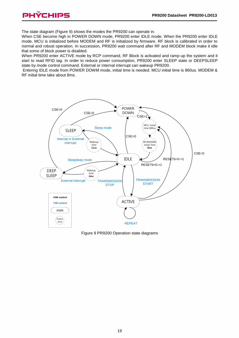
The state diagram (Figure 9) shows the modes the PR9200 can operate in.
When CSE become high in POWER DOWN mode, PR9200 enter IDLE mode. When the PR9200 enter IDLE
mode, MCU is initialized before MODEM and RF is initialized by firmware. RF block is calibrated in order to
normal and robust operation. In succession, PR9200 wait command after RF and MODEM block make it idle
that some of block power is disabled.
When PR9200 enter ACTIVE mode by RCP command, RF Block is activated and ramp-up the system and it
start to read RFID tag. In order to reduce power consumption, PR9200 enter SLEEP state or DEEPSLEEP
state by mode control command. External or internal interrupt can wakeup PR9200.
Entering IDLE mode from POWER DOWM mode, initial time is needed. MCU initial time is 860us. MODEM &
RF initial time take about 8ms.
POWER DOWN
IDLE
SLEEP
CSE=0
H/W control
F/W control
CSE=0
CSE=1
MCU initial time 860us
RF/MODEM initial time
8ms
state
Transi-tion
Internal or External
interrupt
Sleep mode
Sleepdeep mode
External interrupt TRANSMISSION
START
CSE=0CSE=0
TRANSMISSION
STOP
RESETb=0->1
DEEP SLEEP
ACTIVE
RESETb=0->1
REPEAT
Wakeup time11us
Wakeup time4ms
Figure 9 PR9200 Operation state diagrams
20
PR9200 Datasheet PR9200-LD013
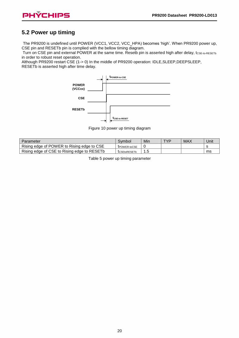
5.2 Power up timing The PR9200 is undefined until POWER (VCC1, VCC2, VCC_HPA) becomes ‘high’. When PR9200 power up, CSE pin and RESETb pin is complied with the bellow timing diagram. Turn on CSE pin and external POWER at the same time. Resetb pin is asserted high after delay, tCSE-to-RESETb in order to robust reset operation. Although PR9200 restart CSE (1-> 0) In the middle of PR9200 operation: IDLE,SLEEP,DEEPSLEEP, RESETb is asserted high after time delay.
POWER
(VCCxx)
CSE
RESETb
tPOWER-to-CSE
tCSE-to-RESET
Figure 10 power up timing diagram
Parameter Symbol Min TYP MAX Unit
Rising edge of POWER to Rising edge to CSE tPOWER-toCSE 0 s
Rising edge of CSE to Rising edge to RESETb tCSEtoRESETb 1.5 ms
Table 5 power up timing parameter
21
PR9200 Datasheet PR9200-LD013
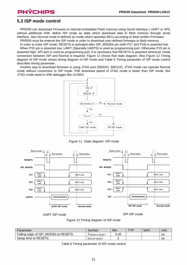
5.3 ISP mode control
PR9200 can download Firmware to internal embedded Flash memory using Serial interface ( UART or SPI)
without additional H/W. define ISP mode as state which download data to flash memory through serial
interface. Also Normal mode is defined as mode which operates MCU according to flash-written Firmware.
PR9200 must be entered the ISP mode in order to download user-defined firmware to flash memory.
In order to enter ISP mode, RESETb is activated after ISP_MODEb pin (with P17 and P16) is asserted low.
When P15 pin is asserted low, UART (Specially UART0) is used as programming port. Otherwise P15 pin is
asserted high, SPI port is used as programming port. It is necessary that RESETb is asserted whenever mode
conversion between ISP and Normal is required. Figure 11 shows that state diagram. Also Figure 12 Timing
diagram of ISP mode shows timing diagram of ISP mode and Table 6 Timing parameter of ISP mode control
describes timing parameter.
Another way to download firmware is using JTAG port (SWDIO, SWCLK). JTAG mode can operate Normal
mode without conversion to ISP mode. F/W download speed of JTAG mode is faster than ISP mode. But
JTAG mode need to H/W debugger like ULINK2.
CSEor
RESETb
ISP_MODEb=0 ?
YES
NO
P15=0 ?
Normal mode
YES
NO
UART ISP mode SPI ISP mode
Figure 11 State diagram: ISP mode
Don't care
ISP_MODEb
RESETb
P17
P16
P15
Don't care
Don't care
UART0 PROGRAMMING
Don't care
Don't care
Don't care
UART ISP mode Normal mode
tMODE-to-RESET
tSETUP-RESET tSETUP-RESET
UART ISP mode
Don't care
ISP_MODEb
RESETb
P17
P16
P15
Don't care
Don't care
SPI
Don't care
Don't care
Don't care
SPI ISP mode Normal mode
PROGRAMMING
tMODE-to-RESET
tSETUP-RESET tSETUP-RESET
SPI ISP mode
Figure 12 Timing diagram of ISP mode
Parameter Symbol Min TYP MAX Unit
Falling edge of ISP_MODEb to RESETb TMODE-to-RESET 0.45 us
Setup time to RESETb tSETUP-RESET 2 us
Table 6 Timing parameter of ISP mode control
22
PR9200 Datasheet PR9200-LD013
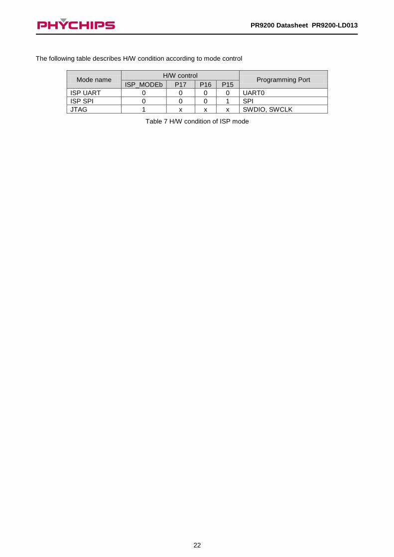
The following table describes H/W condition according to mode control
Mode name H/W control
Programming Port ISP_MODEb P17 P16 P15
ISP UART 0 0 0 0 UART0
ISP SPI 0 0 0 1 SPI
JTAG 1 x x x SWDIO, SWCLK
Table 7 H/W condition of ISP mode
23
PR9200 Datasheet PR9200-LD013
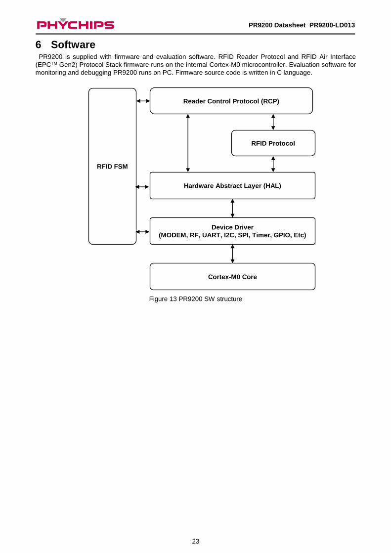
6 Software PR9200 is supplied with firmware and evaluation software. RFID Reader Protocol and RFID Air Interface
(EPCTM Gen2) Protocol Stack firmware runs on the internal Cortex-M0 microcontroller. Evaluation software for
monitoring and debugging PR9200 runs on PC. Firmware source code is written in C language.
Figure 13 PR9200 SW structure
Cortex-M0 Core
RFID Protocol
Device Driver
(MODEM, RF, UART, I2C, SPI, Timer, GPIO, Etc)
Hardware Abstract Layer (HAL)
Reader Control Protocol (RCP)
RFID FSM
24
PR9200 Datasheet PR9200-LD013
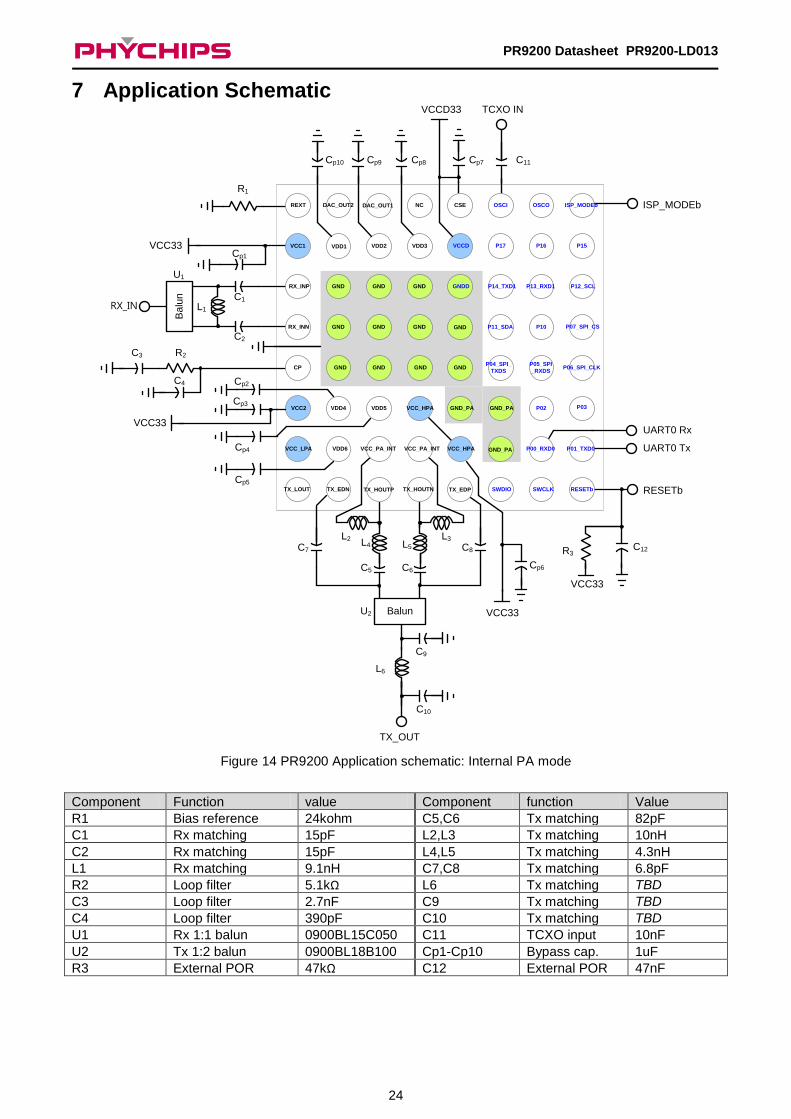
7 Application Schematic
RX_IN
Ba
lun
R1
VCC33
VCC33
TX_OUT
VCC33
RESETb
UART0 Rx
UART0 Tx
VCCD33
Cp1
C1
C2
L1
C3
C4
R2
Cp2
Cp4
L2 L3L4 L5
U1
U2
C5 C6
C7 C8
C9
C10
L6
Cp7
VCC1 VDD2 VDD3VDD1
GNDRX_INP
RX_INN
GNDGND
GND
VCC2
GNDGND
VDD4
CP GND GND
GND
VDD5
VCC_LPA GND_PA
GND_PA
TX_HOUTPTX_EDN TX_HOUTN TX_EDP
VCC_PA_INT VCC_PA_INT
GND_PA
VDD6 VCC_HPA
SWDIO SWCLK
GNDD
VCCD
RESETb
P00_RXD0 P01_TXD0
P02 P03
P04_SPI_
TXDSP06_SPI_CLK
P05_SPI
_RXDS
P07_SPI_CS
P12_SCL
P11_SDA
P13_RXD1
P10
P15
P14_TXD1
P17 P16
ISP_MODEbOSCOOSCICSENCDAC_OUT1DAC_OUT2REXT
GND
VCC_HPA
TX_LOUT
GND
Balun
TCXO IN
Cp6
Cp3
ISP_MODEb
C11Cp8Cp9Cp10
Cp5
VCC33
C12R3
Figure 14 PR9200 Application schematic: Internal PA mode
Component Function value Component function Value
R1 Bias reference 24kohm C5,C6 Tx matching 82pF
C1 Rx matching 15pF L2,L3 Tx matching 10nH
C2 Rx matching 15pF L4,L5 Tx matching 4.3nH
L1 Rx matching 9.1nH C7,C8 Tx matching 6.8pF
R2 Loop filter 5.1kΩ L6 Tx matching TBD
C3 Loop filter 2.7nF C9 Tx matching TBD
C4 Loop filter 390pF C10 Tx matching TBD
U1 Rx 1:1 balun 0900BL15C050 C11 TCXO input 10nF
U2 Tx 1:2 balun 0900BL18B100 Cp1-Cp10 Bypass cap. 1uF
R3 External POR 47kΩ C12 External POR 47nF
25
PR9200 Datasheet PR9200-LD013
RX_IN
Ba
lun
R1
VCC33
VCC33
TX_OUT
VCC33
RESETb
UART0 Rx
UART0 Tx
VCCD33
Cp1
C1
C2
L1
C3
C4
R2
Cp2
Cp4
L2
L3
L4
L5
U1
U2
C
5
C6
C7 C8
C9
C10
L6
Cp7
VCC1 VDD2 VDD3VDD1
GNDRX_INP
RX_INN
GNDGND
GND
VCC2
GNDGND
VDD4
CP GND GND
GND
VDD5
VCC_LPA GND_PA
GND_PA
TX_HOUTPTX_EDN TX_HOUTN TX_EDP
VCC_PA_INT VCC_PA_INT
GND_PA
VDD6 VCC_HPA
SWDIO SWCLK
GNDD
VCCD
RESETb
P00_RXD0 P01_TXD0
P02 P03
P04_SPI_
TXDS
P06_SPI_CL
K
P05_SPI
_RXDS
P07_SPI_C
S
P12_SCL
P11_SDA
P13_RXD1
P10
P15
P14_TXD1
P17 P16
ISP_MODEbOSCOOSCICSENCDAC_OUT1DAC_OUT2REXT
GND
VCC_HPA
TX_LOUT
GND
Balun
TCXO IN
Cp6
Cp3
ISP_MODEb
C11Cp8Cp9Cp10
U3
Cp5
VCC33
C12R3
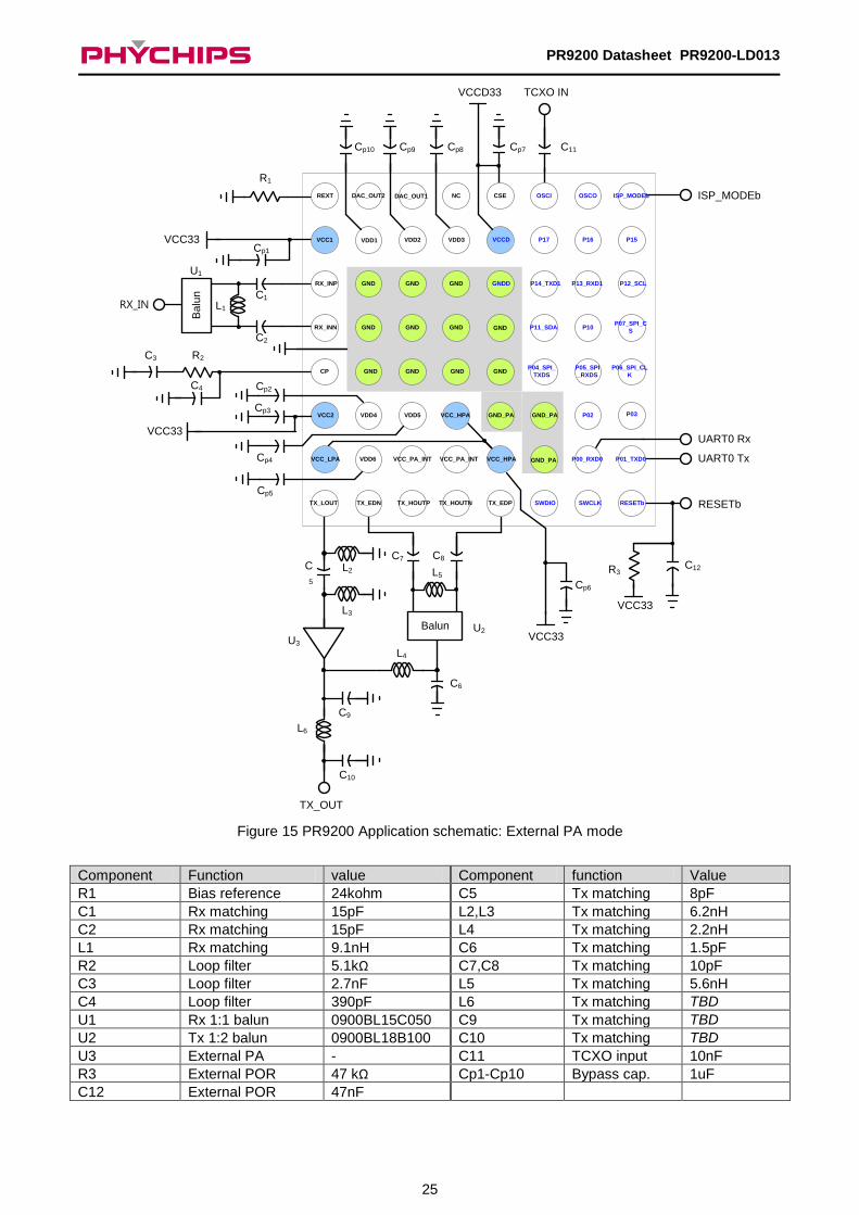
Figure 15 PR9200 Application schematic: External PA mode
Component Function value Component function Value
R1 Bias reference 24kohm C5 Tx matching 8pF
C1 Rx matching 15pF L2,L3 Tx matching 6.2nH
C2 Rx matching 15pF L4 Tx matching 2.2nH
L1 Rx matching 9.1nH C6 Tx matching 1.5pF
R2 Loop filter 5.1kΩ C7,C8 Tx matching 10pF
C3 Loop filter 2.7nF L5 Tx matching 5.6nH
C4 Loop filter 390pF L6 Tx matching TBD
U1 Rx 1:1 balun 0900BL15C050 C9 Tx matching TBD
U2 Tx 1:2 balun 0900BL18B100 C10 Tx matching TBD
U3 External PA - C11 TCXO input 10nF
R3 External POR 47 kΩ Cp1-Cp10 Bypass cap. 1uF
C12 External POR 47nF
26
PR9200 Datasheet PR9200-LD013
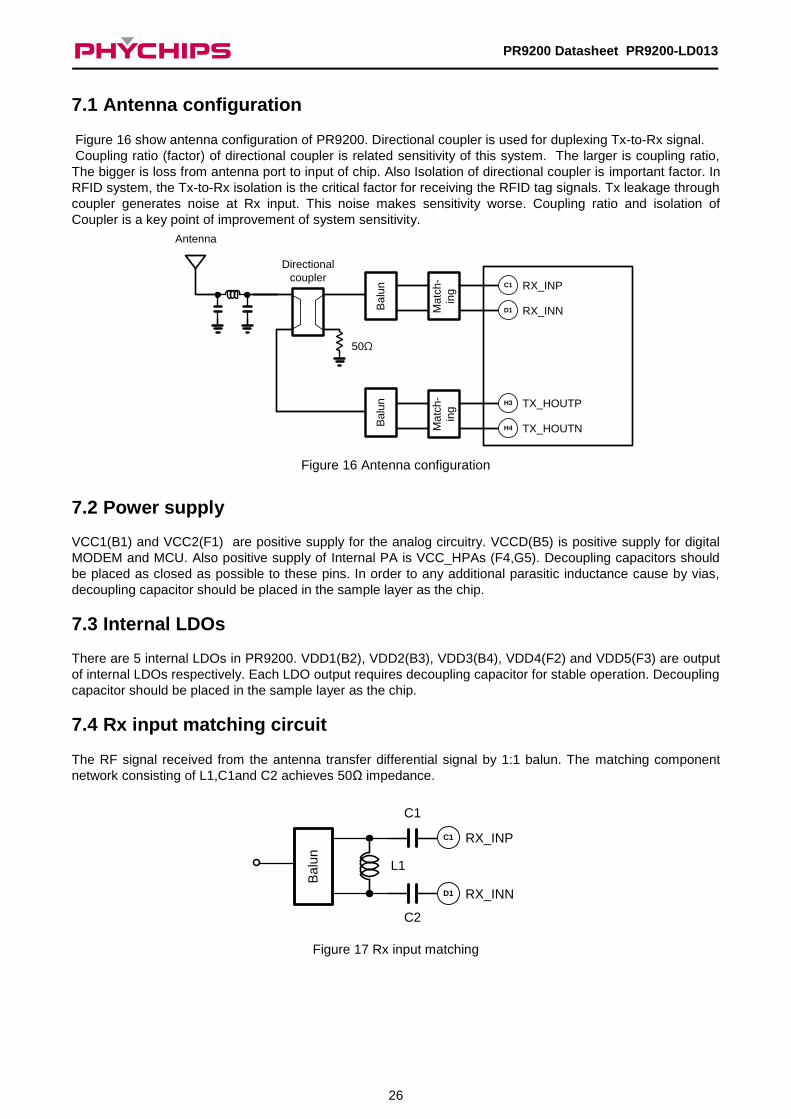
7.1 Antenna configuration
Figure 16 show antenna configuration of PR9200. Directional coupler is used for duplexing Tx-to-Rx signal.
Coupling ratio (factor) of directional coupler is related sensitivity of this system. The larger is coupling ratio,
The bigger is loss from antenna port to input of chip. Also Isolation of directional coupler is important factor. In
RFID system, the Tx-to-Rx isolation is the critical factor for receiving the RFID tag signals. Tx leakage through
coupler generates noise at Rx input. This noise makes sensitivity worse. Coupling ratio and isolation of
Coupler is a key point of improvement of system sensitivity.
Antenna
Directional
coupler
Ba
lun RX_INP
RX_INN
Ba
lun
Ma
tch-
ing
C1
D1
Ma
tch
-
ing
H3
H4
TX_HOUTP
TX_HOUTN
50Ω
Figure 16 Antenna configuration
7.2 Power supply
VCC1(B1) and VCC2(F1) are positive supply for the analog circuitry. VCCD(B5) is positive supply for digital
MODEM and MCU. Also positive supply of Internal PA is VCC_HPAs (F4,G5). Decoupling capacitors should
be placed as closed as possible to these pins. In order to any additional parasitic inductance cause by vias,
decoupling capacitor should be placed in the sample layer as the chip.
7.3 Internal LDOs
There are 5 internal LDOs in PR9200. VDD1(B2), VDD2(B3), VDD3(B4), VDD4(F2) and VDD5(F3) are output
of internal LDOs respectively. Each LDO output requires decoupling capacitor for stable operation. Decoupling
capacitor should be placed in the sample layer as the chip.
7.4 Rx input matching circuit
The RF signal received from the antenna transfer differential signal by 1:1 balun. The matching component
network consisting of L1,C1and C2 achieves 50Ω impedance.
Ba
lun
RX_INP
RX_INN
C1
D1
L1
C1
C2
Figure 17 Rx input matching
27
PR9200 Datasheet PR9200-LD013
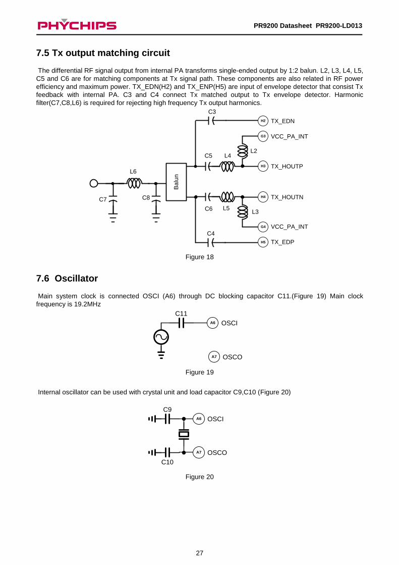
7.5 Tx output matching circuit
The differential RF signal output from internal PA transforms single-ended output by 1:2 balun. L2, L3, L4, L5,
C5 and C6 are for matching components at Tx signal path. These components are also related in RF power
efficiency and maximum power. TX_EDN(H2) and TX_ENP(H5) are input of envelope detector that consist Tx
feedback with internal PA. C3 and C4 connect Tx matched output to Tx envelope detector. Harmonic
filter(C7,C8,L6) is required for rejecting high frequency Tx output harmonics.
H3
H4
TX_HOUTP
TX_HOUTN
L2
L3
L4
L5
C5
C6
C3
C4
C8C7
L6B
alu
n
H2 TX_EDN
H5 TX_EDP
G3 VCC_PA_INT
G4 VCC_PA_INT
Figure 18
7.6 Oscillator
Main system clock is connected OSCI (A6) through DC blocking capacitor C11.(Figure 19) Main clock
frequency is 19.2MHz
OSCIA6
C11
A7 OSCO
Figure 19
Internal oscillator can be used with crystal unit and load capacitor C9,C10 (Figure 20)
A6
A7
OSCI
OSCO
C9
C10
Figure 20
28
PR9200 Datasheet PR9200-LD013
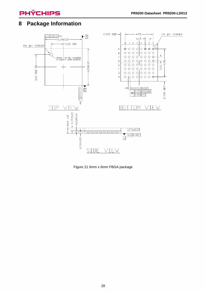
8 Package Information
Figure 21 6mm x 6mm FBGA package
29
PR9200 Datasheet PR9200-LD013
9 Address Information
PHYCHIPS Inc.
#204 Migun Techno World 1, 533 Yongsan-dong, Yuseong-gu, Daejeon, Korea, 305-500
http://www.phychips.com
Tel: +82-42-864-2402
Fax: +82-42-864-2403
Disclaimer: PHYCHIPS reserves the right to make changes to the information in this document without prior
notice. The purchase of PHYCHIPS products does not convey any license under patent rights owned by
PHYCHIPS or others. PHYCHIPS does not assume any responsibility for the use of this product. It is the
customer’s responsibility to make sure that the system complies with regulations.
© 2012 PHYCHIPS Inc. All rights reserved. The reproduction of this document is NOT allowed without approval
of PHYCHIPS Inc.