Dual PLL Precision Synthesizer Data Sheet AD9578 · Dual PLL Precision Synthesizer Data Sheet...
44
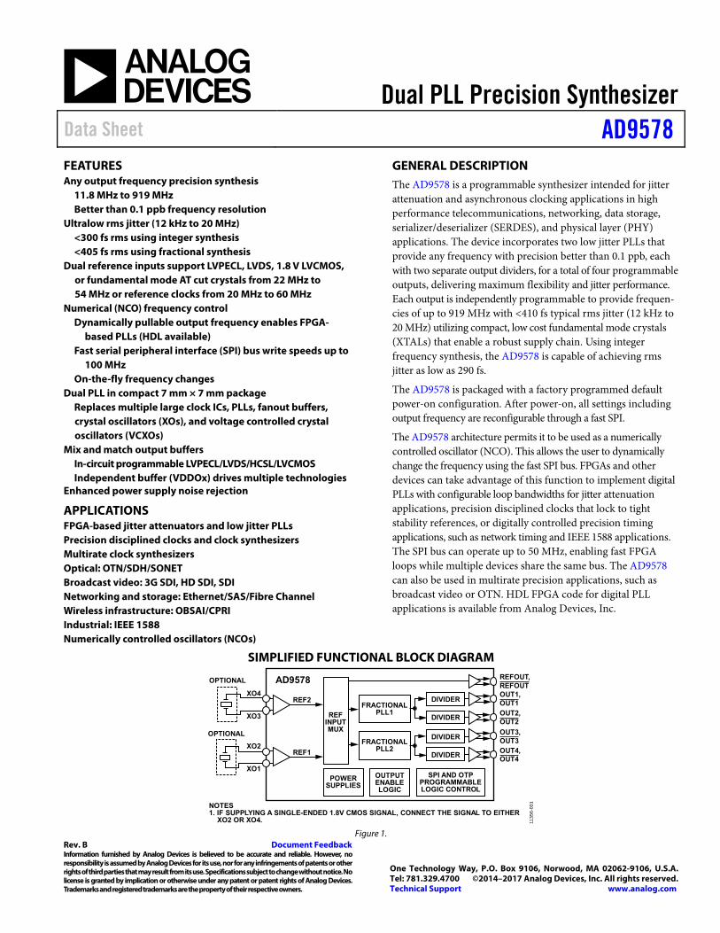
Dual PLL Precision Synthesizer Data Sheet AD9578 Rev. B Document Feedback Information furnished by Analog Devices is believed to be accurate and reliable. However, no responsibility is assumed by Analog Devices for its use, nor for any infringements of patents or other rights of third parties that may result from its use. Specifications subject to change without notice. No license is granted by implication or otherwise under any patent or patent rights of Analog Devices. Trademarks and registered trademarks are the property of their respective owners. One Technology Way, P.O. Box 9106, Norwood, MA 02062-9106, U.S.A. Tel: 781.329.4700 ©2014–2017 Analog Devices, Inc. All rights reserved. Technical Support www.analog.com FEATURES Any output frequency precision synthesis 11.8 MHz to 919 MHz Better than 0.1 ppb frequency resolution Ultralow rms jitter (12 kHz to 20 MHz) <300 fs rms using integer synthesis <405 fs rms using fractional synthesis Dual reference inputs support LVPECL, LVDS, 1.8 V LVCMOS, or fundamental mode AT cut crystals from 22 MHz to 54 MHz or reference clocks from 20 MHz to 60 MHz Numerical (NCO) frequency control Dynamically pullable output frequency enables FPGA- based PLLs (HDL available) Fast serial peripheral interface (SPI) bus write speeds up to 100 MHz On-the-fly frequency changes Dual PLL in compact 7 mm × 7 mm package Replaces multiple large clock ICs, PLLs, fanout buffers, crystal oscillators (XOs), and voltage controlled crystal oscillators (VCXOs) Mix and match output buffers In-circuit programmable LVPECL/LVDS/HCSL/LVCMOS Independent buffer (VDDOx) drives multiple technologies Enhanced power supply noise rejection APPLICATIONS FPGA-based jitter attenuators and low jitter PLLs Precision disciplined clocks and clock synthesizers Multirate clock synthesizers Optical: OTN/SDH/SONET Broadcast video: 3G SDI, HD SDI, SDI Networking and storage: Ethernet/SAS/Fibre Channel Wireless infrastructure: OBSAI/CPRI Industrial: IEEE 1588 Numerically controlled oscillators (NCOs) GENERAL DESCRIPTION The AD9578 is a programmable synthesizer intended for jitter attenuation and asynchronous clocking applications in high performance telecommunications, networking, data storage, serializer/deserializer (SERDES), and physical layer (PHY) applications. The device incorporates two low jitter PLLs that provide any frequency with precision better than 0.1 ppb, each with two separate output dividers, for a total of four programmable outputs, delivering maximum flexibility and jitter performance. Each output is independently programmable to provide frequen- cies of up to 919 MHz with <410 fs typical rms jitter (12 kHz to 20 MHz) utilizing compact, low cost fundamental mode crystals (XTALs) that enable a robust supply chain. Using integer frequency synthesis, the AD9578 is capable of achieving rms jitter as low as 290 fs. The AD9578 is packaged with a factory programmed default power-on configuration. After power-on, all settings including output frequency are reconfigurable through a fast SPI. The AD9578 architecture permits it to be used as a numerically controlled oscillator (NCO). This allows the user to dynamically change the frequency using the fast SPI bus. FPGAs and other devices can take advantage of this function to implement digital PLLs with configurable loop bandwidths for jitter attenuation applications, precision disciplined clocks that lock to tight stability references, or digitally controlled precision timing applications, such as network timing and IEEE 1588 applications. The SPI bus can operate up to 50 MHz, enabling fast FPGA loops while multiple devices share the same bus. The AD9578 can also be used in multirate precision applications, such as broadcast video or OTN. HDL FPGA code for digital PLL applications is available from Analog Devices, Inc. SIMPLIFIED FUNCTIONAL BLOCK DIAGRAM OPTIONAL NOTES 1. IF SUPPLYING A SINGLE-ENDED 1.8V CMOS SIGNAL, CONNECT THE SIGNAL TO EITHER XO2 OR XO4. OPTIONAL XO4 XO3 XO2 XO1 REF1 AD9578 REF2 REF INPUT MUX POWER SUPPLIES OUTPUT ENABLE LOGIC SPI AND OTP PROGRAMMABLE LOGIC CONTROL FRACTIONAL PLL2 FRACTIONAL PLL1 DIVIDER OUT1, DIVIDER REFOUT, OUT2, DIVIDER OUT3, DIVIDER OUT4, OUT1 REFOUT OUT2 OUT3 OUT4 11356-001 Figure 1.
Transcript of Dual PLL Precision Synthesizer Data Sheet AD9578 · Dual PLL Precision Synthesizer Data Sheet...
Dual PLL Precision SynthesizerData Sheet AD9578
Rev. B Document Feedback Information furnished by Analog Devices is believed to be accurate and reliable. However, no responsibility is assumed by Analog Devices for its use, nor for any infringements of patents or other rights of third parties that may result from its use. Specifications subject to change without notice. No license is granted by implication or otherwise under any patent or patent rights of Analog Devices. Trademarks and registered trademarks are the property of their respective owners.
One Technology Way, P.O. Box 9106, Norwood, MA 02062-9106, U.S.A.Tel: 781.329.4700 ©2014–2017 Analog Devices, Inc. All rights reserved. Technical Support www.analog.com
FEATURES Any output frequency precision synthesis
11.8 MHz to 919 MHz Better than 0.1 ppb frequency resolution
Ultralow rms jitter (12 kHz to 20 MHz) <300 fs rms using integer synthesis <405 fs rms using fractional synthesis
Dual reference inputs support LVPECL, LVDS, 1.8 V LVCMOS, or fundamental mode AT cut crystals from 22 MHz to 54 MHz or reference clocks from 20 MHz to 60 MHz
Numerical (NCO) frequency control Dynamically pullable output frequency enables FPGA-
based PLLs (HDL available) Fast serial peripheral interface (SPI) bus write speeds up to
100 MHz On-the-fly frequency changes
Dual PLL in compact 7 mm × 7 mm package Replaces multiple large clock ICs, PLLs, fanout buffers, crystal oscillators (XOs), and voltage controlled crystal oscillators (VCXOs)
Mix and match output buffers In-circuit programmable LVPECL/LVDS/HCSL/LVCMOS Independent buffer (VDDOx) drives multiple technologies
Enhanced power supply noise rejection
APPLICATIONS FPGA-based jitter attenuators and low jitter PLLs Precision disciplined clocks and clock synthesizers Multirate clock synthesizers Optical: OTN/SDH/SONET Broadcast video: 3G SDI, HD SDI, SDI Networking and storage: Ethernet/SAS/Fibre Channel Wireless infrastructure: OBSAI/CPRI Industrial: IEEE 1588 Numerically controlled oscillators (NCOs)
GENERAL DESCRIPTION The AD9578 is a programmable synthesizer intended for jitter attenuation and asynchronous clocking applications in high performance telecommunications, networking, data storage, serializer/deserializer (SERDES), and physical layer (PHY) applications. The device incorporates two low jitter PLLs that provide any frequency with precision better than 0.1 ppb, each with two separate output dividers, for a total of four programmable outputs, delivering maximum flexibility and jitter performance. Each output is independently programmable to provide frequen-cies of up to 919 MHz with <410 fs typical rms jitter (12 kHz to 20 MHz) utilizing compact, low cost fundamental mode crystals (XTALs) that enable a robust supply chain. Using integer frequency synthesis, the AD9578 is capable of achieving rms jitter as low as 290 fs.
The AD9578 is packaged with a factory programmed default power-on configuration. After power-on, all settings including output frequency are reconfigurable through a fast SPI.
The AD9578 architecture permits it to be used as a numerically controlled oscillator (NCO). This allows the user to dynamically change the frequency using the fast SPI bus. FPGAs and other devices can take advantage of this function to implement digital PLLs with configurable loop bandwidths for jitter attenuation applications, precision disciplined clocks that lock to tight stability references, or digitally controlled precision timing applications, such as network timing and IEEE 1588 applications. The SPI bus can operate up to 50 MHz, enabling fast FPGA loops while multiple devices share the same bus. The AD9578 can also be used in multirate precision applications, such as broadcast video or OTN. HDL FPGA code for digital PLL applications is available from Analog Devices, Inc.
SIMPLIFIED FUNCTIONAL BLOCK DIAGRAM
OPTIONAL
NOTES1. IF SUPPLYING A SINGLE-ENDED 1.8V CMOS SIGNAL, CONNECT THE SIGNAL TO EITHER XO2 OR XO4.
OPTIONAL
XO4
XO3
XO2
XO1
REF1
AD9578
REF2
REFINPUTMUX
POWERSUPPLIES
OUTPUTENABLELOGIC
SPI AND OTPPROGRAMMABLELOGIC CONTROL
FRACTIONALPLL2
FRACTIONALPLL1
DIVIDEROUT1,
DIVIDER
REFOUT,
OUT2,
DIVIDEROUT3,
DIVIDEROUT4,
OUT1
REFOUT
OUT2
OUT3
OUT4
1135
6-00
1
Figure 1.
AD9578 Data Sheet
Rev. B | Page 2 of 44
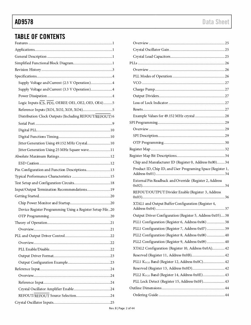
TABLE OF CONTENTS Features .....................................................................................1 Applications...............................................................................1 General Description ..................................................................1 Simplified Functional Block Diagram........................................1 Revision History ........................................................................3 Specifications .............................................................................4
Supply Voltage and Current (2.5 V Operation) ......................4 Supply Voltage and Current (3.3 V Operation) ......................4 Power Dissipation ..................................................................4 Logic Inputs (CS, PD1, OEREF, OE1, OE2, OE3, OE4) .........5 Reference Inputs (XO1, XO2, XO3, XO4) ..............................5 Distribution Clock Outputs (Including REFOUT/REFOUT) 6 Serial Port ..............................................................................9 Digital PLL...........................................................................10 Digital Functions Timing.....................................................10 Jitter Generation Using 49.152 MHz Crystal........................10 Jitter Generation Using 25 MHz Square wave ......................11
Absolute Maximum Ratings ....................................................12 ESD Caution ........................................................................12
Pin Configuration and Function Descriptions.........................13 Typical Performance Characteristics .......................................15 Test Setup and Configuration Circuits.....................................18 Input/Output Termination Recommendations ........................19 Getting Started.........................................................................20
Chip Power Monitor and Startup .........................................20 Device Register Programming Using a Register Setup File ..20 OTP Programming ..............................................................20
Theory of Operation................................................................21 Overview..............................................................................21
PLL and Output Driver Control ..............................................22 Overview..............................................................................22 PLL Enable/Disable..............................................................22 Output Driver Format..........................................................23 Output Configuration Example ...........................................23
Reference Input........................................................................24 Overview..............................................................................24 Reference Input ....................................................................24 Crystal Oscillator Amplifier Enable .....................................24 REFOUT/REFOUT Source Selection...................................24
Crystal Oscillator Inputs..........................................................25
Overview ............................................................................. 25 Crystal Oscillator Gain ........................................................ 25 Crystal Load Capacitors....................................................... 25
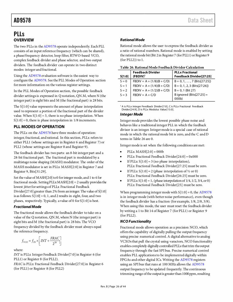
PLLs ........................................................................................ 26 Overview ............................................................................. 26 PLL Modes of Operation ..................................................... 26 VCO .................................................................................... 27 Charge Pump....................................................................... 27 Output Dividers................................................................... 27 Loss of Lock Indicator ......................................................... 27 Resets................................................................................... 27 Example Values for 49.152 MHz crystal .............................. 28
SPI Programming .................................................................... 29 Overview ............................................................................. 29 SPI Description.................................................................... 29 OTP Programming .............................................................. 30
Register Map ........................................................................... 32 Register Map Bit Descriptions ................................................. 34
Chip and Manufacturer ID (Register 0, Address 0x00)........ 34 Product ID, Chip ID, and User Programing Space (Register 1, Address 0x01) ...................................................................... 34 External Pin Readback and Override (Register 2, Address 0x02).................................................................................... 34 REFOUT/OUTPUT Divider Enable (Register 3, Address 0x03).................................................................................... 36 XTAL1 and Output Buffer Configuration (Register 4, Address 0x04) ...................................................................... 37 Output Driver Configuration (Register 5, Address 0x05) .... 38 PLL1 Configuration (Register 6, Address 0x06) .................. 38 PLL1 Configuration (Register 7, Address 0x07) .................. 39 PLL2 Configuration (Register 8, Address 0x08) .................. 40 PLL2 Configuration (Register 9, Address 0x09) .................. 40 XTAL2 Configuration (Register 10, Address 0x0A)............. 42 Reserved (Register 11, Address 0x0B).................................. 42 PLL1 KVCO Band (Register 12, Address 0x0C)...................... 42 Reserved (Register 13, Address 0x0D) ................................. 42 PLL2 KVCO Band (Register 14, Address 0x0E) ...................... 43 PLL Lock Detect (Register 15, Address 0x0F)...................... 43
Outline Dimensions ................................................................ 44 Ordering Guide ................................................................... 44
Data Sheet AD9578
Rev. B | Page 3 of 44
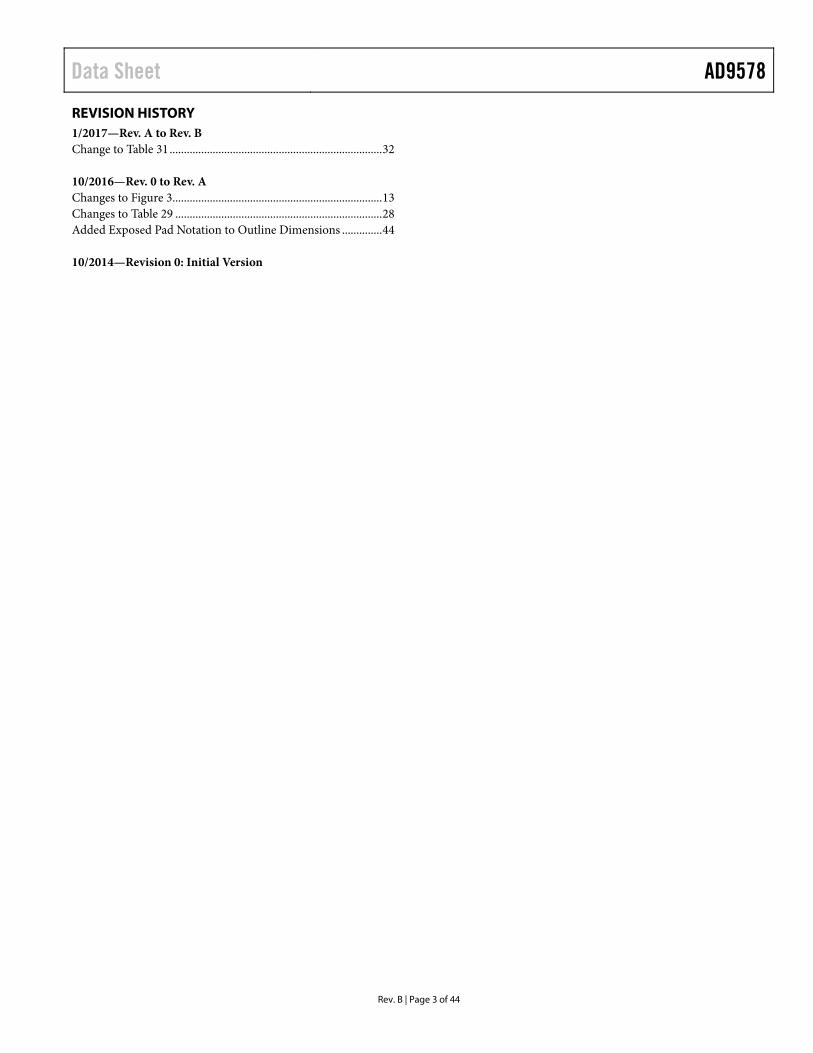
REVISION HISTORY 1/2017—Rev. A to Rev. B Change to Table 31 .......................................................................... 32 10/2016—Rev. 0 to Rev. A Changes to Figure 3 ......................................................................... 13 Changes to Table 29 ........................................................................ 28 Added Exposed Pad Notation to Outline Dimensions .............. 44 10/2014—Revision 0: Initial Version
AD9578 Data Sheet
Rev. B | Page 4 of 44
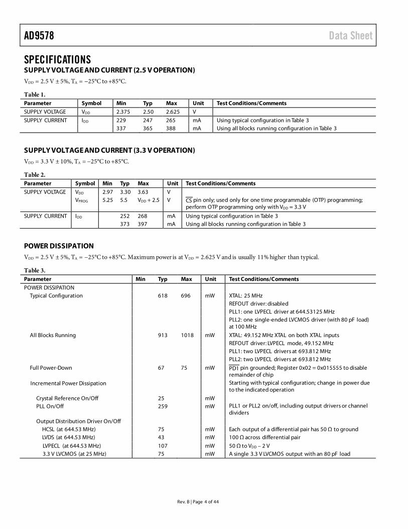
SPECIFICATIONS SUPPLY VOLTAGE AND CURRENT (2.5 V OPERATION) VDD = 2.5 V ± 5%, TA = −25°C to +85°C.
Table 1. Parameter Symbol Min Typ Max Unit Test Conditions/Comments
SUPPLY VOLTAGE VDD 2.375 2.50 2.625 V
SUPPLY CURRENT IDD 229 247 265 mA Using typical configuration in Table 3 337 365 388 mA Using all blocks running configuration in Table 3
SUPPLY VOLTAGE AND CURRENT (3.3 V OPERATION) VDD = 3.3 V ± 10%, TA = −25°C to +85°C.
Table 2. Parameter Symbol Min Typ Max Unit Test Conditions/Comments
SUPPLY VOLTAGE VDD 2.97 3.30 3.63 V VPROG 5.25 5.5 VDD + 2.5 V CS pin only; used only for one time programmable (OTP) programming;
perform OTP programming only with VDD = 3.3 V
SUPPLY CURRENT IDD 252 268 mA Using typical configuration in Table 3 373 397 mA Using all blocks running configuration in Table 3
POWER DISSIPATION VDD = 2.5 V ± 5%, TA = −25°C to +85°C. Maximum power is at VDD = 2.625 V and is usually 11% higher than typical.
Table 3. Parameter Min Typ Max Unit Test Conditions/Comments
POWER DISSIPATION Typical Configuration 618 696 mW XTAL: 25 MHz REFOUT driver: disabled PLL1: one LVPECL driver at 644.53125 MHz
PLL2: one single-ended LVCMOS driver (with 80 pF load) at 100 MHz
All Blocks Running 913 1018 mW XTAL: 49.152 MHz XTAL on both XTAL inputs REFOUT driver: LVPECL mode, 49.152 MHz PLL1: two LVPECL drivers at 693.812 MHz PLL2: two LVPECL drivers at 693.812 MHz
Full Power-Down 67 75 mW PD1 pin grounded; Register 0x02 = 0x015555 to disable remainder of chip
Incremental Power Dissipation Starting with typical configuration; change in power due to the indicated operation
Crystal Reference On/Off 25 mW PLL On/Off 259 mW PLL1 or PLL2 on/off, including output drivers or channel
dividers
Output Distribution Driver On/Off HCSL (at 644.53 MHz) 75 mW Each output of a differential pair has 50 Ω to ground LVDS (at 644.53 MHz) 43 mW 100 Ω across differential pair
LVPECL (at 644.53 MHz) 107 mW 50 Ω to VDD – 2 V 3.3 V LVCMOS (at 25 MHz) 75 mW A single 3.3 V LVCMOS output with an 80 pF load
Data Sheet AD9578
Rev. B | Page 5 of 44
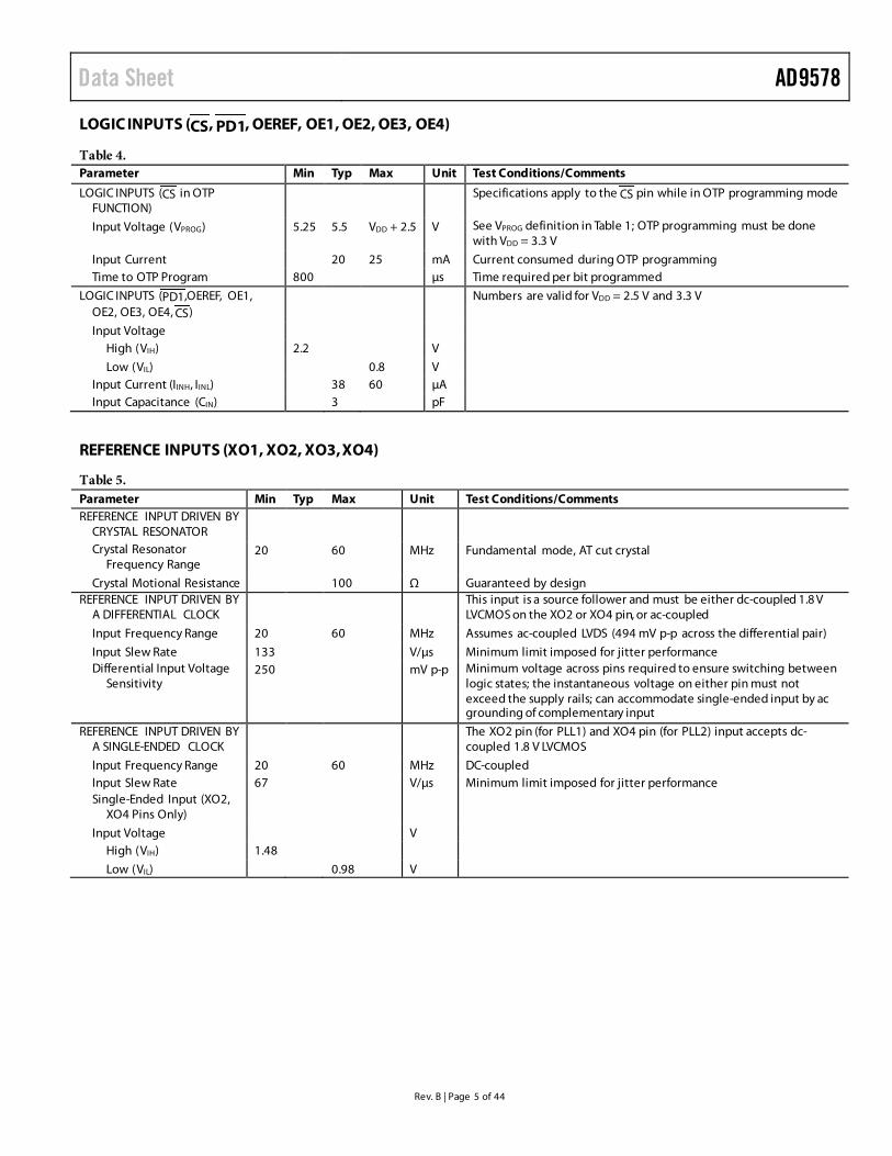
LOGIC INPUTS (CS, PD1, OEREF, OE1, OE2, OE3, OE4)
Table 4. Parameter Min Typ Max Unit Test Conditions/Comments
LOGIC INPUTS (CS in OTP FUNCTION)
Specifications apply to the CS pin while in OTP programming mode
Input Voltage (VPROG) 5.25 5.5 VDD + 2.5 V See VPROG definition in Table 1; OTP programming must be done with VDD = 3.3 V
Input Current 20 25 mA Current consumed during OTP programming Time to OTP Program 800 µs Time required per bit programmed
LOGIC INPUTS (PD1,OEREF, OE1, OE2, OE3, OE4, CS)
Numbers are valid for VDD = 2.5 V and 3.3 V
Input Voltage High (VIH) 2.2 V
Low (VIL) 0.8 V Input Current (IINH, IINL) 38 60 µA Input Capacitance (CIN) 3 pF
REFERENCE INPUTS (XO1, XO2, XO3, XO4)
Table 5. Parameter Min Typ Max Unit Test Conditions/Comments REFERENCE INPUT DRIVEN BY
CRYSTAL RESONATOR
Crystal Resonator Frequency Range
20 60 MHz Fundamental mode, AT cut crystal
Crystal Motional Resistance 100 Ω Guaranteed by design REFERENCE INPUT DRIVEN BY
A DIFFERENTIAL CLOCK This input is a source follower and must be either dc-coupled 1.8 V
LVCMOS on the XO2 or XO4 pin, or ac-coupled
Input Frequency Range 20 60 MHz Assumes ac-coupled LVDS (494 mV p-p across the differential pair)
Input Slew Rate 133 V/μs Minimum limit imposed for jitter performance Differential Input Voltage
Sensitivity 250 mV p-p Minimum voltage across pins required to ensure switching between
logic states; the instantaneous voltage on either pin must not exceed the supply rails; can accommodate single-ended input by ac grounding of complementary input
REFERENCE INPUT DRIVEN BY A SINGLE-ENDED CLOCK
The XO2 pin (for PLL1) and XO4 pin (for PLL2) input accepts dc-coupled 1.8 V LVCMOS
Input Frequency Range 20 60 MHz DC-coupled Input Slew Rate 67 V/μs Minimum limit imposed for jitter performance Single-Ended Input (XO2,
XO4 Pins Only)
Input Voltage V High (VIH) 1.48
Low (VIL) 0.98 V
AD9578 Data Sheet
Rev. B | Page 6 of 44
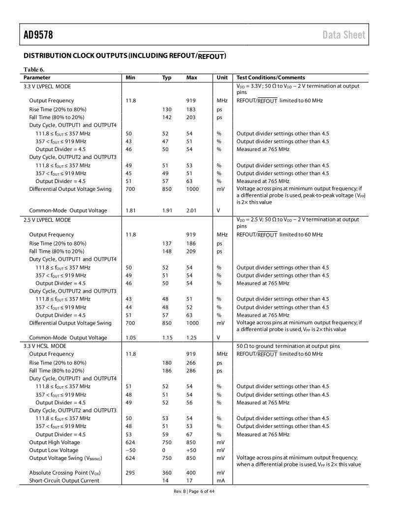
DISTRIBUTION CLOCK OUTPUTS (INCLUDING REFOUT/REFOUT)
Table 6. Parameter Min Typ Max Unit Test Conditions/Comments
3.3 V LVPECL MODE VDD = 3.3V ; 50 Ω to VDD − 2 V termination at output pins
Output Frequency 11.8 919 MHz REFOUT/REFOUT limited to 60 MHz
Rise Time (20% to 80%) 130 183 ps Fall Time (80% to 20%) 142 203 ps Duty Cycle, OUTPUT1 and OUTPUT4
111.8 ≤ fOUT ≤ 357 MHz 50 52 54 % Output divider settings other than 4.5 357 < fOUT ≤ 919 MHz 43 47 51 % Output divider settings other than 4.5 Output Divider = 4.5 46 50 54 % Measured at 765 MHz
Duty Cycle, OUTPUT2 and OUTPUT3
111.8 ≤ fOUT ≤ 357 MHz 49 51 53 % Output divider settings other than 4.5 357 < fOUT ≤ 919 MHz 45 49 51 % Output divider settings other than 4.5 Output Divider = 4.5 51 57 63 % Measured at 765 MHz
Differential Output Voltage Swing 700 850 1000 mV Voltage across pins at minimum output frequency; if a differential probe is used, peak-to-peak voltage (VPP) is 2× this value
Common-Mode Output Voltage 1.81 1.91 2.01 V
2.5 V LVPECL MODE VDD = 2.5 V; 50 Ω to VDD − 2 V termination at output pins
Output Frequency 11.8 919 MHz REFOUT/REFOUT limited to 60 MHz
Rise Time (20% to 80%) 137 186 ps Fall Time (80% to 20%) 148 209 ps Duty Cycle, OUTPUT1 and OUTPUT4
111.8 ≤ fOUT ≤ 357 MHz 50 52 54 % Output divider settings other than 4.5 357 < fOUT ≤ 919 MHz 49 51 54 % Output divider settings other than 4.5 Output Divider = 4.5 46 50 54 % Measured at 765 MHz
Duty Cycle, OUTPUT2 and OUTPUT3 111.8 ≤ fOUT ≤ 357 MHz 43 48 51 % Output divider settings other than 4.5
357 < fOUT ≤ 919 MHz 44 48 52 % Output divider settings other than 4.5 Output Divider = 4.5 51 57 63 % Measured at 765 MHz
Differential Output Voltage Swing 700 850 1000 mV Voltage across pins at minimum output frequency; if a differential probe is used, VPP is 2× this value
Common-Mode Output Voltage 1.05 1.15 1.25 V
3.3 V HCSL MODE 50 Ω to ground termination at output pins Output Frequency 11.8 919 MHz REFOUT/REFOUT limited to 60 MHz
Rise Time (20% to 80%) 180 266 ps Fall Time (80% to 20%) 186 286 ps Duty Cycle, OUTPUT1 and OUTPUT4
111.8 ≤ fOUT ≤ 357 MHz 51 52 54 % Output divider settings other than 4.5
357 < fOUT ≤ 919 MHz 48 51 54 % Output divider settings other than 4.5 Output Divider = 4.5 49 52 56 % Measured at 765 MHz
Duty Cycle, OUTPUT2 and OUTPUT3 111.8 ≤ fOUT ≤ 357 MHz 50 53 54 % Output divider settings other than 4.5 357 < fOUT ≤ 919 MHz 48 51 53 % Output divider settings other than 4.5
Output Divider = 4.5 53 59 67 % Measured at 765 MHz Output High Voltage 624 750 850 mV Output Low Voltage −50 0 +50 mV Output Voltage Swing (VSWING) 624 750 850 mV Voltage across pins at minimum output frequency;
when a differential probe is used, VPP is 2× this value
Absolute Crossing Point (VOX) 295 360 400 mV Short-Circuit Output Current 14 17 mA
Data Sheet AD9578
Rev. B | Page 7 of 44
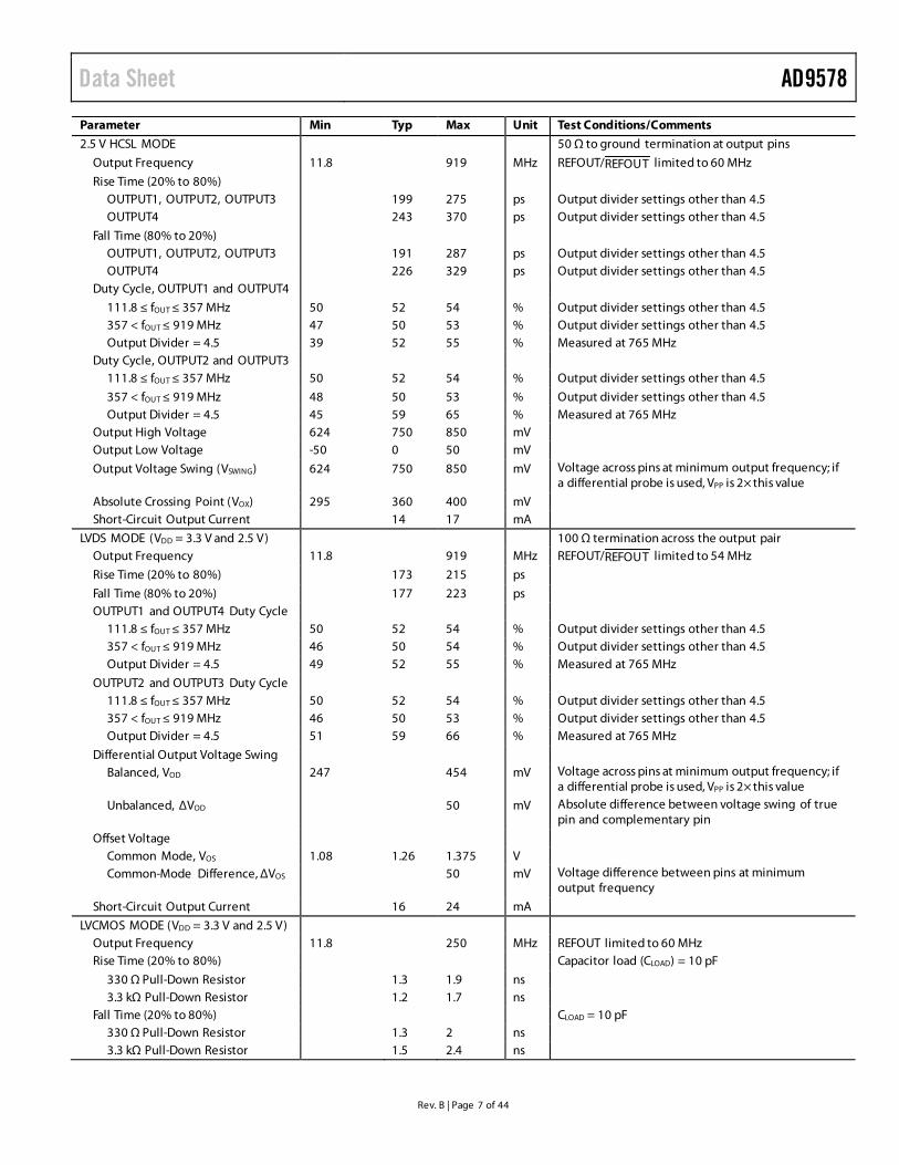
Parameter Min Typ Max Unit Test Conditions/Comments
2.5 V HCSL MODE 50 Ω to ground termination at output pins
Output Frequency 11.8 919 MHz REFOUT/REFOUT limited to 60 MHz
Rise Time (20% to 80%) OUTPUT1, OUTPUT2, OUTPUT3 199 275 ps Output divider settings other than 4.5 OUTPUT4 243 370 ps Output divider settings other than 4.5
Fall Time (80% to 20%) OUTPUT1, OUTPUT2, OUTPUT3 191 287 ps Output divider settings other than 4.5 OUTPUT4 226 329 ps Output divider settings other than 4.5
Duty Cycle, OUTPUT1 and OUTPUT4
111.8 ≤ fOUT ≤ 357 MHz 50 52 54 % Output divider settings other than 4.5 357 < fOUT ≤ 919 MHz 47 50 53 % Output divider settings other than 4.5 Output Divider = 4.5 39 52 55 % Measured at 765 MHz
Duty Cycle, OUTPUT2 and OUTPUT3 111.8 ≤ fOUT ≤ 357 MHz 50 52 54 % Output divider settings other than 4.5
357 < fOUT ≤ 919 MHz 48 50 53 % Output divider settings other than 4.5 Output Divider = 4.5 45 59 65 % Measured at 765 MHz
Output High Voltage 624 750 850 mV Output Low Voltage -50 0 50 mV
Output Voltage Swing (VSWING) 624 750 850 mV Voltage across pins at minimum output frequency; if a differential probe is used, VPP is 2× this value
Absolute Crossing Point (VOX) 295 360 400 mV Short-Circuit Output Current 14 17 mA
LVDS MODE (VDD = 3.3 V and 2.5 V) 100 Ω termination across the output pair Output Frequency 11.8 919 MHz REFOUT/REFOUT limited to 54 MHz
Rise Time (20% to 80%) 173 215 ps
Fall Time (80% to 20%) 177 223 ps OUTPUT1 and OUTPUT4 Duty Cycle
111.8 ≤ fOUT ≤ 357 MHz 50 52 54 % Output divider settings other than 4.5 357 < fOUT ≤ 919 MHz 46 50 54 % Output divider settings other than 4.5 Output Divider = 4.5 49 52 55 % Measured at 765 MHz
OUTPUT2 and OUTPUT3 Duty Cycle 111.8 ≤ fOUT ≤ 357 MHz 50 52 54 % Output divider settings other than 4.5 357 < fOUT ≤ 919 MHz 46 50 53 % Output divider settings other than 4.5 Output Divider = 4.5 51 59 66 % Measured at 765 MHz
Differential Output Voltage Swing Balanced, VOD 247 454 mV Voltage across pins at minimum output frequency; if
a differential probe is used, VPP is 2× this value
Unbalanced, ΔVOD 50 mV Absolute difference between voltage swing of true pin and complementary pin
Offset Voltage Common Mode, VOS 1.08 1.26 1.375 V Common-Mode Difference, ΔVOS 50 mV Voltage difference between pins at minimum
output frequency
Short-Circuit Output Current 16 24 mA
LVCMOS MODE (VDD = 3.3 V and 2.5 V) Output Frequency 11.8 250 MHz REFOUT limited to 60 MHz Rise Time (20% to 80%) Capacitor load (CLOAD) = 10 pF
330 Ω Pull-Down Resistor 1.3 1.9 ns 3.3 kΩ Pull-Down Resistor 1.2 1.7 ns
Fall Time (20% to 80%) CLOAD = 10 pF 330 Ω Pull-Down Resistor 1.3 2 ns 3.3 kΩ Pull-Down Resistor 1.5 2.4 ns
AD9578 Data Sheet
Rev. B | Page 8 of 44
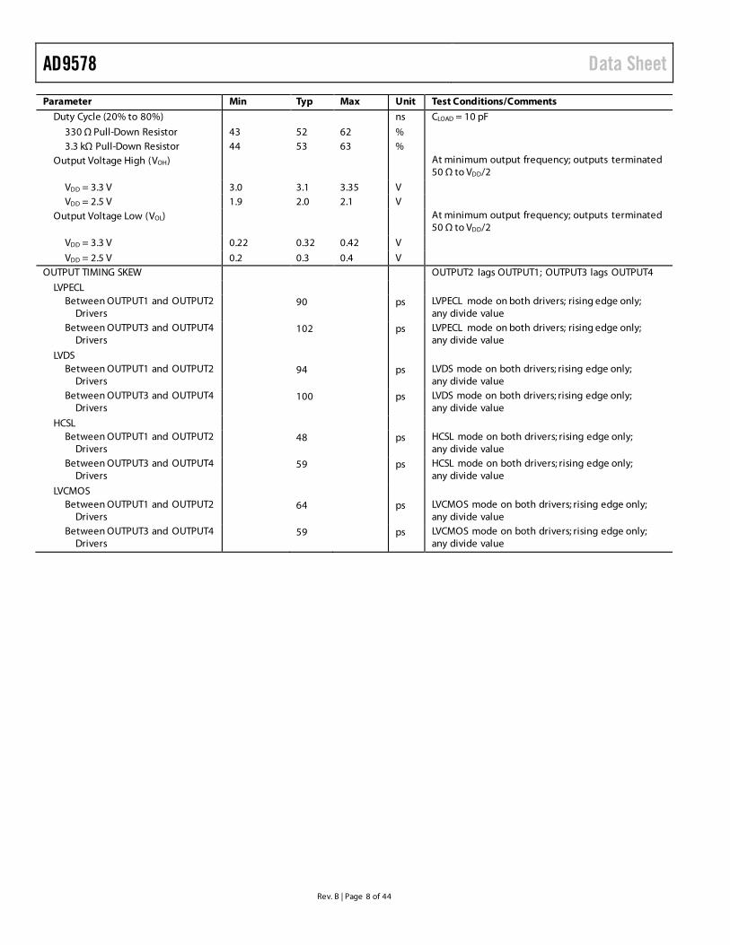
Parameter Min Typ Max Unit Test Conditions/Comments
Duty Cycle (20% to 80%) ns CLOAD = 10 pF
330 Ω Pull-Down Resistor 43 52 62 % 3.3 kΩ Pull-Down Resistor 44 53 63 %
Output Voltage High (VOH) At minimum output frequency; outputs terminated 50 Ω to VDD/2
VDD = 3.3 V 3.0 3.1 3.35 V VDD = 2.5 V 1.9 2.0 2.1 V
Output Voltage Low (VOL) At minimum output frequency; outputs terminated 50 Ω to VDD/2
VDD = 3.3 V 0.22 0.32 0.42 V
VDD = 2.5 V 0.2 0.3 0.4 V OUTPUT TIMING SKEW OUTPUT2 lags OUTPUT1; OUTPUT3 lags OUTPUT4
LVPECL Between OUTPUT1 and OUTPUT2
Drivers 90 ps LVPECL mode on both drivers; rising edge only;
any divide value Between OUTPUT3 and OUTPUT4
Drivers 102 ps LVPECL mode on both drivers; rising edge only;
any divide value
LVDS Between OUTPUT1 and OUTPUT2
Drivers 94 ps LVDS mode on both drivers; rising edge only;
any divide value Between OUTPUT3 and OUTPUT4
Drivers 100 ps LVDS mode on both drivers; rising edge only;
any divide value
HCSL Between OUTPUT1 and OUTPUT2
Drivers 48 ps HCSL mode on both drivers; rising edge only;
any divide value Between OUTPUT3 and OUTPUT4
Drivers 59 ps HCSL mode on both drivers; rising edge only;
any divide value
LVCMOS Between OUTPUT1 and OUTPUT2
Drivers 64 ps LVCMOS mode on both drivers; rising edge only;
any divide value Between OUTPUT3 and OUTPUT4
Drivers 59 ps LVCMOS mode on both drivers; rising edge only;
any divide value
Data Sheet AD9578
Rev. B | Page 9 of 44
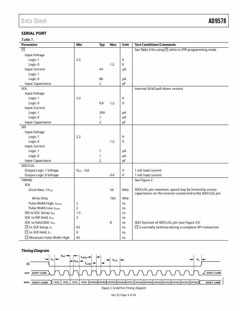
SERIAL PORT Table 7. Parameter Min Typ Max Unit Test Conditions/Comments
CS See Table 4 for using CS while in OTP programming mode
Input Voltage Logic 1 2.2 V Logic 0 1.2 V
Input Current 44 µA
Logic 1 Logic 0 88 µA
Input Capacitance 2 pF
SCK Internal 30 kΩ pull-down resistor Input Voltage
Logic 1 2.2 V
Logic 0 0.8 1.2 V Input Current
Logic 1 200 µA Logic 0 1 µA
Input Capacitance 2 pF SDI
Input Voltage Logic 1 2.2 V Logic 0 1.2 V
Input Current Logic 1 1 µA
Logic 0 1 µA Input Capacitance 2 pF
SDO/LOL Output Logic 1 Voltage VDD − 0.6 V 1 mA load current Output Logic 0 Voltage 0.4 V 1 mA load current
TIMING See Figure 2 SCK
Clock Rate, 1/tCLK 50 MHz SDO/LOL pin maximum speed may be limited by excess capacitance on the receiver connected to the SDO/LOL pin
Write Only 100 MHz
Pulse Width High, tHIGH 2 ns Pulse Width Low, tLOW 2 ns
SDI to SCK Setup, tDS 1.5 ns SCK to SDI Hold, tDH 2 ns
SCK to Valid SDO, tDV 8 ns SDO function of SDO/LOL pin (see Figure 33)
CS to SCK Setup, tS 65 ns CS is normally held low during a complete SPI transaction
CS to SCK Hold, tC 0 ns
CS Minimum Pulse Width High 65 ns
Timing Diagram
tS
DON'T CARE
DON'T CARE
DON'T CARE
DON'T CARE
tDS
tDH
tHIGH
tLOW
tCLK tC
CS
SCK
SDIO DATA[7]ADDR[0] DATA[6] DATA[5] DATA[4] DATA[3] DATA[2] DATA[1] DATA[0]OP[3] OP[2] OP[1] OP[0] ADDR[3] ADDR[2] ADDR[1]
1135
6-13
1
Figure 2. Serial Port Timing Diagram
AD9578 Data Sheet
Rev. B | Page 10 of 44
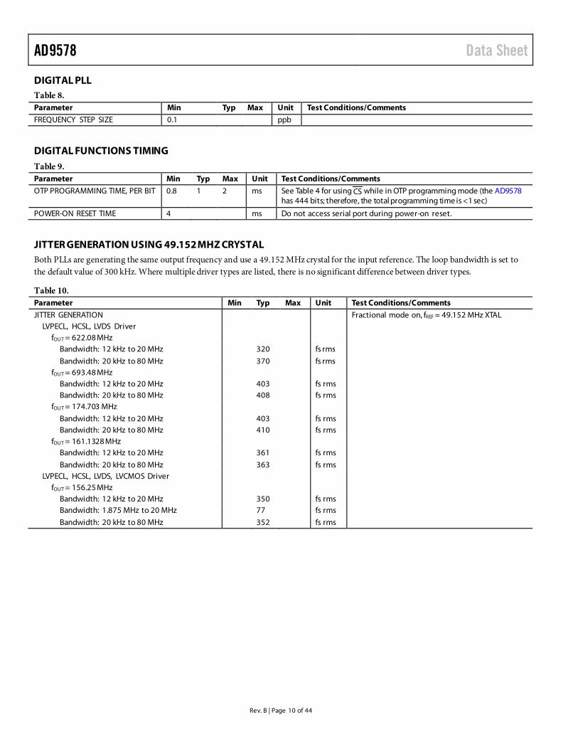
DIGITAL PLL Table 8. Parameter Min Typ Max Unit Test Conditions/Comments
FREQUENCY STEP SIZE 0.1 ppb
DIGITAL FUNCTIONS TIMING Table 9. Parameter Min Typ Max Unit Test Conditions/Comments
OTP PROGRAMMING TIME, PER BIT 0.8 1 2 ms See Table 4 for using CS while in OTP programming mode (the AD9578 has 444 bits; therefore, the total programming time is <1 sec)
POWER-ON RESET TIME 4 ms Do not access serial port during power-on reset.
JITTER GENERATION USING 49.152 MHZ CRYSTAL Both PLLs are generating the same output frequency and use a 49.152 MHz crystal for the input reference. The loop bandwidth is set to the default value of 300 kHz. Where multiple driver types are listed, there is no significant difference between driver types.
Table 10. Parameter Min Typ Max Unit Test Conditions/Comments
JITTER GENERATION Fractional mode on, fREF = 49.152 MHz XTAL LVPECL, HCSL, LVDS Driver
fOUT = 622.08 MHz Bandwidth: 12 kHz to 20 MHz 320 fs rms
Bandwidth: 20 kHz to 80 MHz 370 fs rms fOUT = 693.48 MHz
Bandwidth: 12 kHz to 20 MHz 403 fs rms Bandwidth: 20 kHz to 80 MHz 408 fs rms
fOUT = 174.703 MHz
Bandwidth: 12 kHz to 20 MHz 403 fs rms Bandwidth: 20 kHz to 80 MHz 410 fs rms
fOUT = 161.1328 MHz Bandwidth: 12 kHz to 20 MHz 361 fs rms
Bandwidth: 20 kHz to 80 MHz 363 fs rms LVPECL, HCSL, LVDS, LVCMOS Driver
fOUT = 156.25 MHz Bandwidth: 12 kHz to 20 MHz 350 fs rms Bandwidth: 1.875 MHz to 20 MHz 77 fs rms
Bandwidth: 20 kHz to 80 MHz 352 fs rms
Data Sheet AD9578
Rev. B | Page 11 of 44
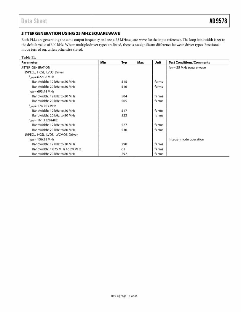
JITTER GENERATION USING 25 MHZ SQUARE WAVE Both PLLs are generating the same output frequency and use a 25 MHz square wave for the input reference. The loop bandwidth is set to the default value of 300 kHz. Where multiple driver types are listed, there is no significant difference between driver types. Fractional mode turned on, unless otherwise stated.
Table 11. Parameter Min Typ Max Unit Test Conditions/Comments
JITTER GENERATION fREF = 25 MHz square wave LVPECL, HCSL, LVDS Driver
fOUT = 622.08 MHz Bandwidth: 12 kHz to 20 MHz 515 fs rms
Bandwidth: 20 kHz to 80 MHz 516 fs rms fOUT = 693.48 MHz
Bandwidth: 12 kHz to 20 MHz 504 fs rms Bandwidth: 20 kHz to 80 MHz 505 fs rms
fOUT = 174.703 MHz Bandwidth: 12 kHz to 20 MHz 517 fs rms Bandwidth: 20 kHz to 80 MHz 523 fs rms
fOUT = 161.1328 MHz Bandwidth: 12 kHz to 20 MHz 527 fs rms
Bandwidth: 20 kHz to 80 MHz 530 fs rms LVPECL, HCSL, LVDS, LVCMOS Driver
fOUT = 156.25 MHz Integer mode operation Bandwidth: 12 kHz to 20 MHz 290 fs rms
Bandwidth: 1.875 MHz to 20 MHz 61 fs rms Bandwidth: 20 kHz to 80 MHz 292 fs rms
AD9578 Data Sheet
Rev. B | Page 12 of 44
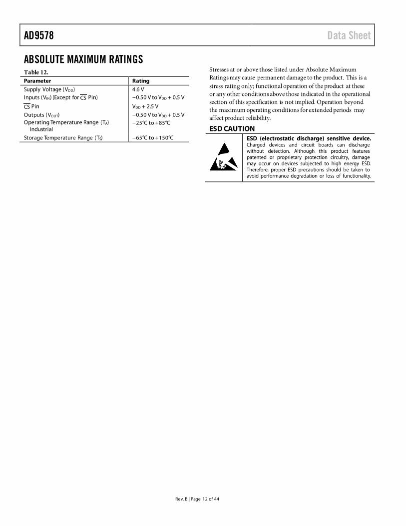
ABSOLUTE MAXIMUM RATINGS Table 12. Parameter Rating
Supply Voltage (VDD) 4.6 V Inputs (VIN) (Except for CS Pin) −0.50 V to VDD + 0.5 V
CS Pin VDD + 2.5 V
Outputs (VOUT) −0.50 V to VDD + 0.5 V Operating Temperature Range (TA)
Industrial −25°C to +85°C
Storage Temperature Range (TS) −65°C to +150°C
Stresses at or above those listed under Absolute Maximum Ratings may cause permanent damage to the product. This is a stress rating only; functional operation of the product at these or any other conditions above those indicated in the operational section of this specification is not implied. Operation beyond the maximum operating conditions for extended periods may affect product reliability.
ESD CAUTION
Data Sheet AD9578
Rev. B | Page 13 of 44
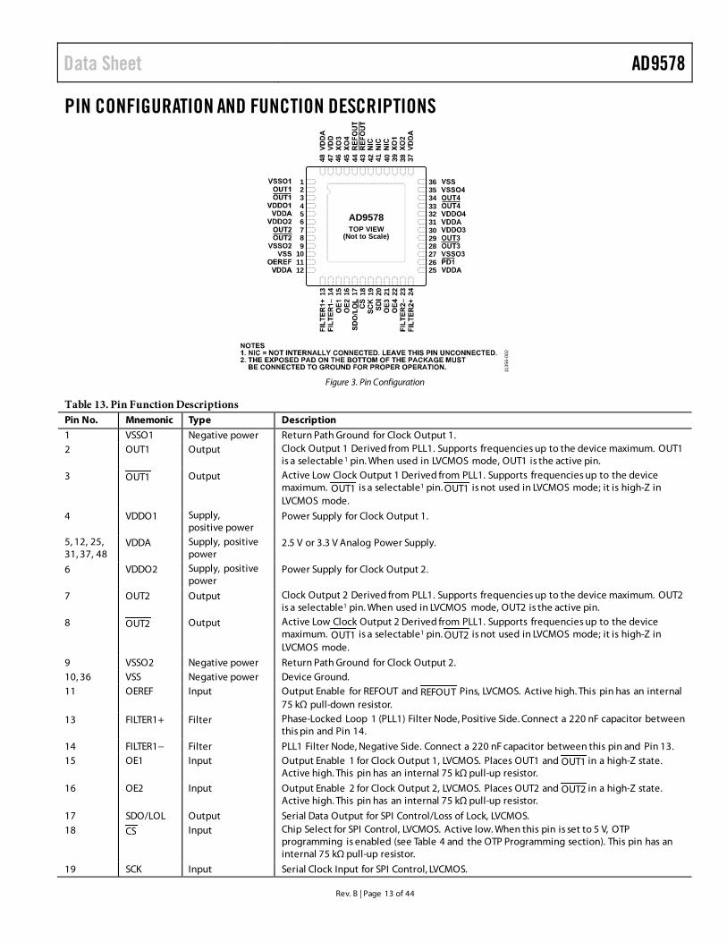
PIN CONFIGURATION AND FUNCTION DESCRIPTIONS
1135
6-00
2
1234567
242322212019181716151413
4445464748 43 42 41 40 39 38 37
TOP VIEW(Not to Scale)
AD9578
252627282930313233343536
89
101112
Figure 3. Pin Configuration
Table 13. Pin Function Descriptions Pin No. Mnemonic Type Description
1 VSSO1 Negative power Return Path Ground for Clock Output 1. 2 OUT1 Output Clock Output 1 Derived from PLL1. Supports frequencies up to the device maximum. OUT1
is a selectable 1 pin. When used in LVCMOS mode, OUT1 is the active pin.
3 OUT1 Output Active Low Clock Output 1 Derived from PLL1. Supports frequencies up to the device maximum. OUT1 is a selectable1 pin. OUT1 is not used in LVCMOS mode; it is high-Z in LVCMOS mode.
4 VDDO1 Supply, positive power
Power Supply for Clock Output 1.
5, 12, 25, 31, 37, 48
VDDA Supply, positive power
2.5 V or 3.3 V Analog Power Supply.
6 VDDO2 Supply, positive power
Power Supply for Clock Output 2.
7 OUT2 Output Clock Output 2 Derived from PLL1. Supports frequencies up to the device maximum. OUT2 is a selectable1 pin. When used in LVCMOS mode, OUT2 is the active pin.
8 OUT2 Output Active Low Clock Output 2 Derived from PLL1. Supports frequencies up to the device maximum. OUT1 is a selectable1 pin. OUT2 is not used in LVCMOS mode; it is high-Z in LVCMOS mode.
9 VSSO2 Negative power Return Path Ground for Clock Output 2. 10, 36 VSS Negative power Device Ground. 11 OEREF Input Output Enable for REFOUT and REFOUT Pins, LVCMOS. Active high. This pin has an internal
75 kΩ pull-down resistor.
13 FILTER1+ Filter Phase-Locked Loop 1 (PLL1) Filter Node, Positive Side. Connect a 220 nF capacitor between this pin and Pin 14.
14 FILTER1− Filter PLL1 Filter Node, Negative Side. Connect a 220 nF capacitor between this pin and Pin 13. 15 OE1 Input Output Enable 1 for Clock Output 1, LVCMOS. Places OUT1 and OUT1 in a high-Z state.
Active high. This pin has an internal 75 kΩ pull-up resistor.
16 OE2 Input Output Enable 2 for Clock Output 2, LVCMOS. Places OUT2 and OUT2 in a high-Z state. Active high. This pin has an internal 75 kΩ pull-up resistor.
17 SDO/LOL Output Serial Data Output for SPI Control/Loss of Lock, LVCMOS. 18 CS Input Chip Select for SPI Control, LVCMOS. Active low. When this pin is set to 5 V, OTP
programming is enabled (see Table 4 and the OTP Programming section). This pin has an internal 75 kΩ pull-up resistor.
19 SCK Input Serial Clock Input for SPI Control, LVCMOS.
AD9578 Data Sheet
Rev. B | Page 14 of 44
Pin No. Mnemonic Type Description
20 SDI Input Serial Data Input for SPI Control, LVCMOS.
21 OE3 Input Output Enable 3 for Clock Output 3, LVCMOS. Places OUT3 and OUT3 in a high-Z state. Active high is the default but active low is programmable. This pin has an internal 75 kΩ pull-up resistor.
22 OE4 Input Output Enable 4 for Clock Output 4, LVCMOS. Places OUT4 and OUT4 in a high-Z state. Active high is the default but active low is programmable. This pin has an internal 75 kΩ pull-up resistor.
23 FILTER2− Filter PLL2 Filter Node, Negative Side. Connect a 220 nF capacitor between this pin and Pin 24.
24 FILTER2+ Filter PLL2 Filter Node, Positive Side. Connect a 220 nF capacitor between this pin and Pin 23. 26 PD1 Input Active Low Power-Down for PLL1, LVCMOS. This pin has an internal 75 kΩ pull-up resistor.
27 VSSO3 Negative power Return Path Ground for Clock Output 3.
28 OUT3 Output Active Low Clock Output 3 Derived from PLL2. Supports frequencies up to the device maximum. OUT3 is a selectable1 pin. OUT3 is not used in LVCMOS mode; it is high-Z in LVCMOS mode.
29 OUT3 Output Clock Output 3 Derived from PLL2. Supports frequencies up to the device maximum. OUT3 is a selectable1 pin. When used in LVCMOS mode, OUT3 is the active pin.
30 VDDO3 Supply, positive power
Power Supply for Clock Output 3.
32 VDDO4 Supply, positive power
Power Supply for Clock Output 4.
33 OUT4 Output Clock Output 4 Derived from PLL2. Supports frequencies up to the device maximum. OUT4 is not used in LVCMOS mode and is high-Z. OUT4 is a selectable1 pin.
34 OUT4 Output Clock Output 4 Derived from PLL2. Supports frequencies up to the device maximum. OUT4 is a selectable1 pin. When used in LVCMOS mode, OUT4 is the active pin.
35 VSSO4 Negative power Return Path Ground for Clock Output 4. 38 XO2 Input Reference Input 1. Connect a crystal across this pin and XO1. Alternatively, the user can
connect a 1.8 V LVCMOS clock to this pin only, or connect a differential, ac-coupled LVDS or LVPECL signal across this pin and the XO1 pin. This pin can be a crystal or reference input.
39 XO1 Input Complementary Reference Input 1. Connect a crystal across this pin and XO2. Alternatively, the user can connect a differential, ac-coupled LVDS or LVPECL signal to this pin and the XO2 pin. This pin can be a crystal or reference input.
40, 41, 42 NIC No Internal Connection. Leave these pins unconnected. 43 REFOUT Output Active Low Reference Clock Output. This pin provides a copy of the reference input or
crystal input frequency. REFOUT is a selectable1 pin.
44 REFOUT Output Reference Clock Output. This pin provides a copy of the reference input or crystal input frequency. REFOUT is a selectable1 pin.
45 XO4 Input Reference Input 2. Connect a crystal across this pin and XO3. Alternatively, connect a 1.8 V LVCMOS clock to this pin only, or connect a differential, ac-coupled LVDS or LVPECL signal across this pin and the XO3 pin. This pin can be a crystal or reference input.
46 XO3 Input Complementary Reference Input 2. Connect a crystal across this pin and XO4. Alternatively, connect a differential, ac-coupled LVDS or LVPECL signal to this pin and the XO4 pin.
47 VDD Supply, positive power
2.5 V or 3.3 V Power Supply for Device Core. This pin can be a crystal or reference input.
EPAD Exposed Pad. The exposed pad on the bottom of the package must be connected to ground for proper operation.
1 Selectable pins are factory programmed to a default power-up configuration. The user can override the default programming to support LVCMOS, LVDS, LVPECL, or
HCSL mode after power-up using the SPI.
Data Sheet AD9578
Rev. B | Page 15 of 44
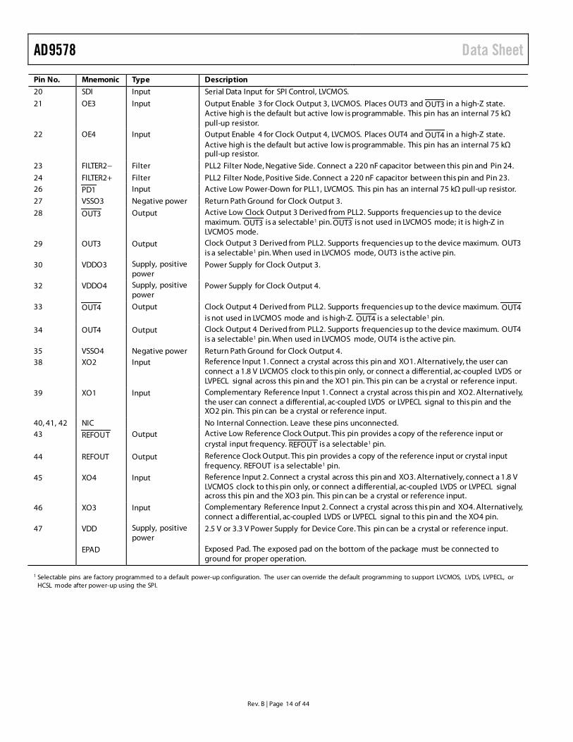
TYPICAL PERFORMANCE CHARACTERISTICS fR is the input reference clock frequency; fOUT is the output clock frequency; VDD at nominal supply voltage (3.3 V). 25 MHz square wave input is a dc-coupled 3.3 V LVCMOS signal with 0.8 ns (20% to 80%) rise time.
PH
AS
E N
OIS
E (
dB
c/H
z)
–70
–160
–80
–90
–100
–110
–120
–130
–140
–150
–1701k100 10M100k10k 1M 100M
FREQUENCY (Hz)
INTEGRATED RMS JITTER(12kHz TO 20MHz): 290fsPHASE NOISE (dBc/Hz):OFFSET100Hz1kHz10kHz100kHz1MHz10MHzFLOOR
LEVEL–116–125–132–133–142–163–164
1135
6-00
3
Figure 4. Absolute Phase Noise (Output Driver = LVDS), fR = 25 MHz Square Wave, fOUT = 156.25 MHz on Both PLLs
PH
AS
E N
OIS
E (
dB
c/H
z)
–70
–170
–80
–90
–100
–110
–120
–130
–140
–150
–160
100 1k 10M100k10k 1M 100M
FREQUENCY (Hz)
INTEGRATED RMS JITTER(12kHz TO 20MHz): 527fsPHASE NOISE (dBc/Hz):OFFSET100Hz1kHz10kHz100kHz1MHz10MHzFLOOR
LEVEL–113–123–127–122–144–163–163
1135
6-00
4
Figure 5. Absolute Phase Noise (Output Driver = LVCMOS), fR = 25 MHz Square Wave, fOUT = 161.1328125 MHz on Both PLLs
PH
AS
E N
OIS
E (
dB
c/H
z)
–70
–170
–80
–90
–100
–110
–120
–130
–140
–150
–160
1k100 10M100k10k 1M 100M
FREQUENCY (Hz)
INTEGRATED RMS JITTER(12kHz TO 20MHz): 517fs
PHASE NOISE (dBc/Hz):OFFSET100Hz1kHz10kHz100kHz1MHz10MHzFLOOR
LEVEL–114–123–128–125–137–162–163
1135
6-00
5
Figure 6. Absolute Phase Noise (Output Driver = LVPECL), fR = 25 MHz Square Wave, fOUT = 174.703 MHz on Both PLLs
1k100 10M100k10k 1M 100M
PH
AS
E N
OIS
E (
dB
c/H
z)
–70
–170
–80
–90
–100
–110
–120
–130
–140
–150
–160
INTEGRATED RMS JITTER(12kHz TO 20MHz): 350fs
PHASE NOISE (dBc/Hz):OFFSET100Hz1kHz10kHz100kHz1MHz10MHzFLOOR
LEVEL–116–121–129–130–141–162–164
1135
6-00
6
FREQUENCY (Hz)
Figure 7. Absolute Phase Noise (Output Driver = LVDS), fR = 49.152 MHz Crystal, fOUT = 156.25 MHz on Both PLLs
PH
AS
E N
OIS
E (
dB
c/H
z)
–70
–170
–80
–90
–100
–110
–120
–130
–140
–150
–160
FREQUENCY (Hz)
INTEGRATED RMS JITTER(12kHz TO 20MHz): 361fs
PHASE NOISE (dBc/Hz):OFFSET100Hz1kHz10kHz100kHz1MHz10MHzFLOOR
LEVEL–104–122–127–129–140–161–163
1135
6-00
7
1k100 10M100k10k 1M 100M
Figure 8. Absolute Phase Noise (Output Driver = 3.3.V LVCMOS), fR = 49.152 MHz Crystal, fOUT = 161.1328125 MHz on Both PLLs
1k100 10M100k10k 1M 100M
PH
AS
E N
OIS
E (
dB
c/H
z)
–70
–170
–80
–90
–100
–110
–120
–130
–140
–150
–160
FREQUENCY (Hz)
INTEGRATED RMS JITTER(12kHz TO 20MHz): 403fs
PHASE NOISE (dBc/Hz):OFFSET100Hz1kHz10kHz100kHz1MHz10MHzFLOOR
LEVEL–105–121–127–126–141–163–165
1135
6-00
8
Figure 9. Absolute Phase Noise (Output Driver = LVPECL), fR = 49.152 MHz Crystal, fOUT = 174.703 MHz on Both PLLs
AD9578 Data Sheet
Rev. B | Page 16 of 44
PHAS
E NO
ISE
(dBc
/Hz)
–60
–70
–160
–80
–90
–100
–110
–120
–130
–140
–150
FREQUENCY (Hz)
INTEGRATED RMS JITTER(12kHz TO 20MHz): 515fsPHASE NOISE (dBc/Hz):OFFSET100Hz1kHz10kHz100kHz1MHz10MHzFLOOR
LEVEL–102–112–115–110–128–155–159
1135
6-00
9
1k100 10M100k10k 1M 100M
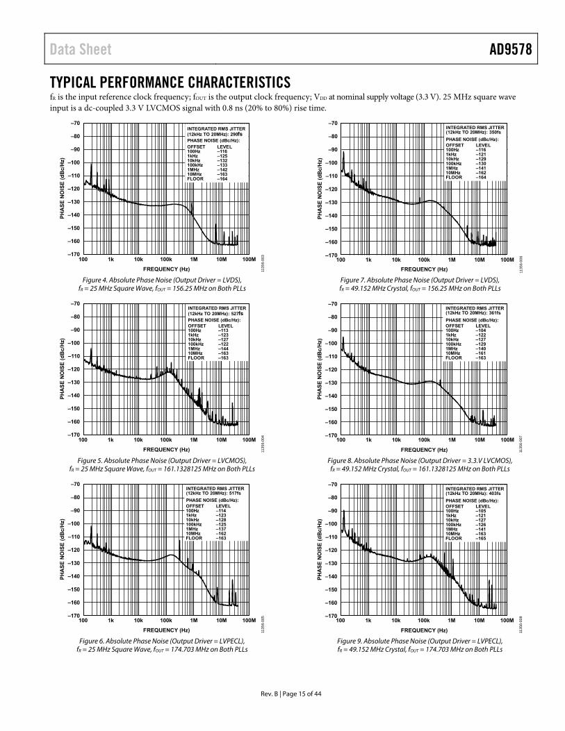
Figure 10. Absolute Phase Noise (Output Driver = LVPECL), fR = 25 MHz 3.3 V LVCMOS Square Wave, fOUT = 622.08 MHz on Both PLLs
1k100 10M100k10k 1M 100M
PHA
SE N
OIS
E (d
Bc/
Hz)
–70
–170
–80
–90
–100
–110
–120
–130
–140
–150
–160
FREQUENCY (Hz)
INTEGRATED RMS JITTER(12kHz TO 20MHz): 504fsPHASE NOISE (dBc/Hz):OFFSET100Hz1kHz10kHz100kHz1MHz10MHzFLOOR
LEVEL–101–111–114–110–127–153–154
1135
6-01
0
Figure 11. Absolute Phase Noise (Output Driver = LVPECL),
fR = 25 MHz Square Wave, fOUT = 693.482991 MHz on Both PLLs
PHA
SE N
OIS
E (d
Bc/
Hz)
–70
–170
–80
–90
–100
–110
–120
–130
–140
–150
–160
FREQUENCY (Hz)
INTEGRATED RMS JITTER(12kHz TO 20MHz): 506fsPHASE NOISE (dBc/Hz):OFFSET100Hz1kHz10kHz100kHz1MHz10MHzFLOOR
LEVEL–101–110–114–110–108–154–160
1135
6-01
11k100 10M100k10k 1M 100M
Figure 12. Absolute Phase Noise (Output Driver = LVPECL),
fR = 25 MHz Square Wave on XO1/XO2 Pins, fOUT = 919 MHz on Both PLLs
1k100 10M100k10k 1M 100M
PHAS
E NO
ISE
(dBc
/Hz)
–60
–70
–160
–80
–90
–100
–110
–120
–130
–140
–150
FREQUENCY (Hz)
INTEGRATED RMS JITTER(12kHz TO 20MHz): 327fsPHASE NOISE (dBc/Hz):OFFSET100Hz1kHz10kHz100kHz1MHz10MHzFLOOR
LEVEL–95–110–116–118–132–155–158
1135
6-01
2
Figure 13. Absolute Phase Noise (Output Driver = LVPECL),
fR = 49.152 MHz Crystal, fOUT = 622.08 MHz on Both PLLs
PHA
SE N
OIS
E (d
Bc/
Hz)
–60
–70
–160
–80
–90
–100
–110
–120
–130
–140
–150
FREQUENCY (Hz)
INTEGRATED RMS JITTER(12kHz TO 20MHz): 392fsPHASE NOISE (dBc/Hz):OFFSET100Hz1kHz10kHz100kHz1MHz10MHzFLOOR
LEVEL–93–110–116–118–125–153–155
1135
6-01
3
1k100 10M100k10k 1M 100M
Figure 14. Absolute Phase Noise (Output Driver = LVPECL),
fR = 49.152 MHz Crystal, fOUT = 693.482991 MHz on Both PLLs
PHA
SE N
OIS
E (d
Bc/
Hz)
–70
–170
–80
–90
–100
–110
–120
–130
–140
–150
–160
FREQUENCY (Hz)
INTEGRATED RMS JITTER(12kHz TO 20MHz): 361fsPHASE NOISE (dBc/Hz):OFFSET100Hz1kHz10kHz100kHz1MHz10MHzFLOOR
LEVEL–93–107–114–116–122–152–159
1 135
6-01
4
1k100 10M100k10k 1M 100M
Figure 15. Absolute Phase Noise (Output Driver = LVPECL),
fR = 49.152 MHz Crystal, fOUT = 919 MHz on Both PLLs
Data Sheet AD9578
Rev. B | Page 17 of 44
PHA
SE N
OIS
E (d
Bc/
Hz)
–60
–70
–80
–90
–100
–110
–120
–130
–140
–150
–160
FREQUENCY (Hz)
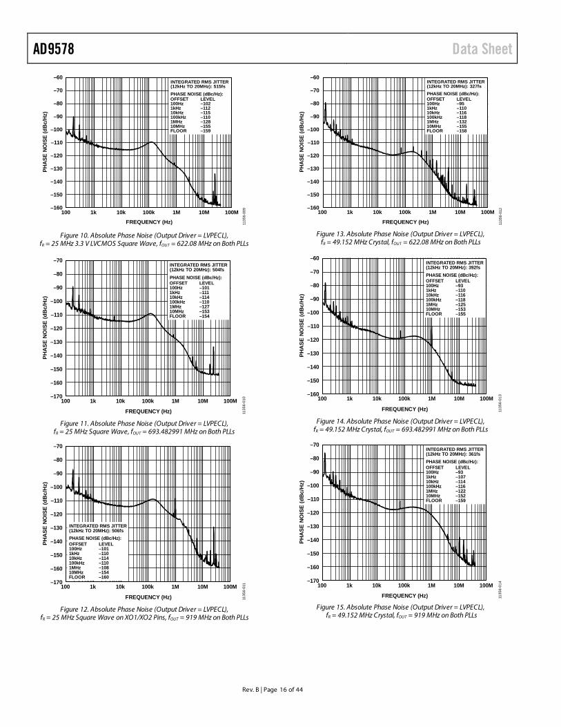
INTEGRATED RMS JITTER(12kHz TO 5MHz): 5.8psPHASE NOISE (dBc/Hz):OFFSET100Hz1kHz10kHz100kHz1MHz10MHzFLOOR
LEVEL–100–110–118–127–130–131–131
1135
6-01
5
1k100 10M100k10k 1M 100M
Figure 16. Phase Noise of 25 MHz, 3.3 V LVCMOS Input Clock Used
DIF
FER
ENTI
ALA
MPL
ITU
DE
(V)
TIME (ns)
–0.4
–0.3
–0.2
–0.1
0
0.1
0.2
0.3
0.4
–2.0 –1.5 –1.0 –0.5 0 0.5 1.0 1.5 2.0 2.5 3.0
1135
6-02
3
Figure 17. Output Waveform, LVDS (400 MHz)
DIF
FER
ENTI
ALA
MPL
ITU
DE
(V)
TIME (ns)
–1.0
–0.8
–0.6
–0.4
–0.2
0
0.2
0.4
0.6
0.8
1.0
–2.0 –1.5 –1.0 –0.5 0 0.5 1.0 1.5 2.0 2.5 3.0
1135
6-02
4
Figure 18. Output Waveform, HCSL (400 MHz)
1135
6-02
5–0.5
0
0.5
1.0
1.5
2.0
2.5
3.0
3.5
4.0
0 1 2 3 4 5 6 7 8 9 10 11 12
AMPL
ITUD
E (V
)
TIME (ns)
10pF LOAD2pF LOAD
Figure 19. Output Waveform, 3.3 V CMOS (100 MHz)
–0.4
–0.3
–0.2
–0.1
0
0.1
0.2
0.3
0.4
0 0.2 0.4 0.6 0.8 1.0 1.2 1.4 1.6 1.8 2.0 2.2
DIF
FER
ENTI
ALA
MPL
ITU
DE
(V)
TIME (ns) 1135
6-04
0
Figure 20. Output Waveform, LVDS (900 MHz)
–1.2
–1.0
–0.8
–0.6
–0.4
–0.2
0
0.2
0.4
0.6
0.8
1.0
1.2
–2.0 –1.5 –1.0 –0.5 0 0.5 1.0 1.5 2.0 2.5 3.0
DIFF
EREN
TIAL
AMPL
ITUD
E (V
)
TIME (ns) 1135
6-04
1
Figure 21. Output Waveform, LVPECL (400 MHz)
AD9578 Data Sheet
Rev. B | Page 18 of 44
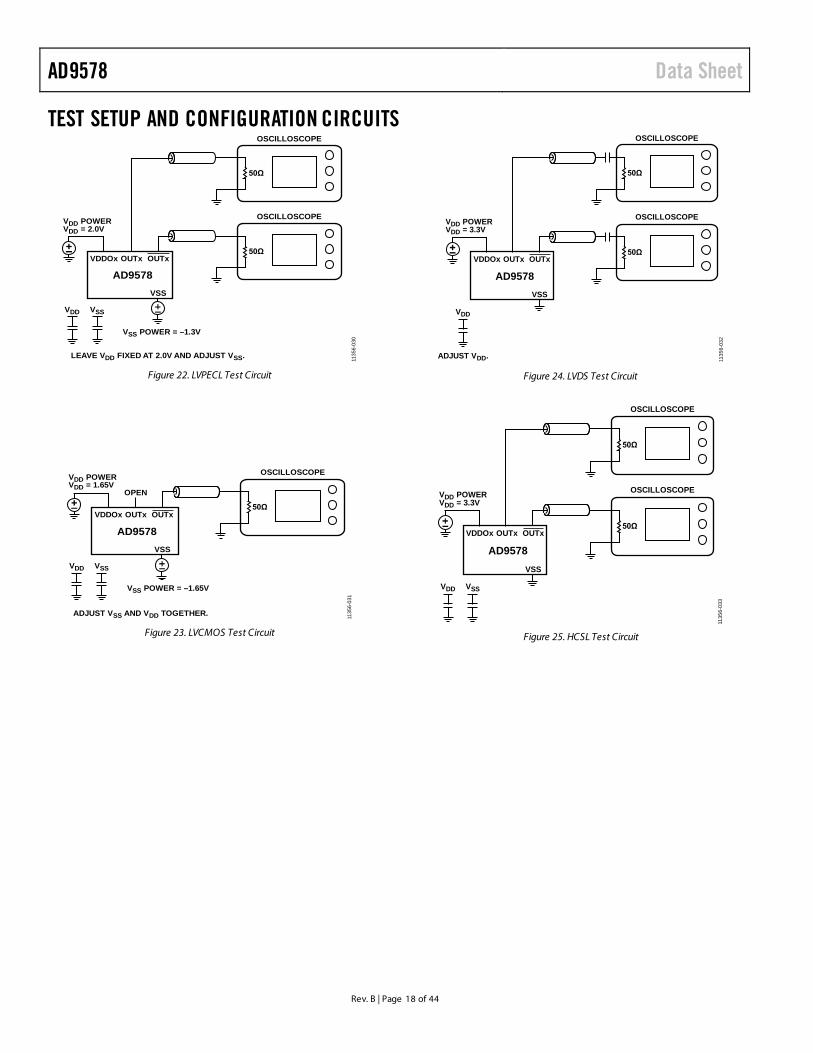
TEST SETUP AND CONFIGURATION CIRCUITS
VDD VSS
50Ω
OSCILLOSCOPE
50Ω
OSCILLOSCOPE
VDDOx OUTx
AD9578OUTx
VSS
VSS POWER = –1.3V
LEAVE VDD FIXED AT 2.0V AND ADJUST VSS.
VDD POWERVDD = 2.0V
1135
6-03
0
Figure 22. LVPECL Test Circuit
VDD VSS
VSS POWER = –1.65V
ADJUST VSS AND VDD TOGETHER.
VDD POWERVDD = 1.65V
OPEN
50Ω
OSCILLOSCOPE
1 135
6-03
1
VDDOx OUTx
AD9578OUTx
VSS
Figure 23. LVCMOS Test Circuit
VDD
50Ω
OSCILLOSCOPE
ADJUST VDD.
VDD POWERVDD = 3.3V
50Ω
OSCILLOSCOPE
1135
6-03
2
VDDOx OUTx
AD9578OUTx
VSS
Figure 24. LVDS Test Circuit
VDD VSS
VDD POWERVDD = 3.3V
50Ω
OSCILLOSCOPE
50Ω
OSCILLOSCOPE
1135
6-03
3
VDDOx OUTx
AD9578OUTx
VSS
Figure 25. HCSL Test Circuit
Data Sheet AD9578
Rev. B | Page 19 of 44
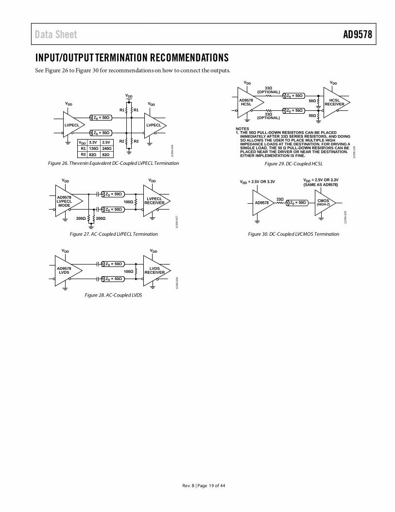
INPUT/OUTPUT TERMINATION RECOMMENDATIONS See Figure 26 to Figure 30 for recommendations on how to connect the outputs.
R1 R1
R2R2
LVPECL LVPECL
VDD
VDD
VDD
VDD 3.3V 2.5VR1R2
240Ω130Ω82Ω82Ω
Z0 = 50Ω
Z0 = 50Ω
1135
6-02
6
Figure 26. Thevenin Equivalent DC-Coupled LVPECL Termination
VDD VDD
AD9578LVPECLMODE
LVPECLRECEIVER100Ω
200Ω 200Ω
Z0 = 50Ω
Z0 = 50Ω
1135
6-02
7
Figure 27. AC-Coupled LVPECL Termination
VDD VDD
AD9578LVDS
LVDSRECEIVER100Ω
Z0 = 50Ω
Z0 = 50Ω
1 135
6-02
8
Figure 28. AC-Coupled LVDS
VDD VDD
AD9578HCSL
HCSLRECEIVER
50Ω
50Ω
33Ω(OPTIONAL)
(OPTIONAL)33Ω
Z0 = 50Ω
Z0 = 50Ω
1135
6-12
8
NOTES1. THE 50Ω PULL-DOWN RESISTORS CAN BE PLACED IMMEDIATELY AFTER 33Ω SERIES RESISTORS, AND DOING SO ALLOWS THE USER TO PLACE MULTIPLE HIGH IMPEDANCE LOADS AT THE DESTINATION. FOR DRIVING A SINGLE LOAD, THE 50 Ω PULL-DOWN RESISTORS CAN BE PLACED NEAR THE DRIVER OR NEAR THE DESTINATION. EITHER IMPLEMENTATION IS FINE.
Figure 29. DC-Coupled HCSL
33ΩAD9578 CMOS
(HIGH-Z)Z0 = 50Ω
VDD = 2.5V OR 3.3V VDD = 2.5V OR 3.3V(SAME AS AD9578)
1135
6-02
9
Figure 30. DC-Coupled LVCMOS Termination
AD9578 Data Sheet
Rev. B | Page 20 of 44
GETTING STARTED CHIP POWER MONITOR AND STARTUP The AD9578 monitors the voltage on the power supplies at power-up. When power supplies are greater than 2.1 V ± 0.1 V, the device generates an internal reset pulse, at which time, the AD9578 loads the values programmed in OTP memory. Do not use the SPI until 4 ms after power-up to ensure that all registers are correctly loaded from the OTP memory and that all internal voltages are stable.
It is possible for the user to overwrite any value stored in the OTP memory if the security bits in Register 0x00 were not set at the time the OTP programming occurred. Take care not to overwrite the factory programmed calibrations (Register 11 through Register 14).
When programming the device through the serial port, write unused or reserved bits to their default values as listed in the register map.
DEVICE REGISTER PROGRAMMING USING A REGISTER SETUP FILE The evaluation software contains a programming wizard and a convenient graphical user interface that assists the user in determining the optimal configuration for the device. It generates a register setup file with a .STP extension that is easily readable using a text editor. These registers can be loaded directly into the AD9578.
OTP PROGRAMMING The AD9578 has 444 bits of OTP memory. OTP stores the nonvolatile default configuration used on power-up.
The default configuration is determined and programmed by the user. Use the SPI to overwrite these bits and change the operation of the AD9578 after power-up. The SPI Programming section describes how the bits affect the device operation and how to use the SPI to modify them.
Data Sheet AD9578
Rev. B | Page 21 of 44
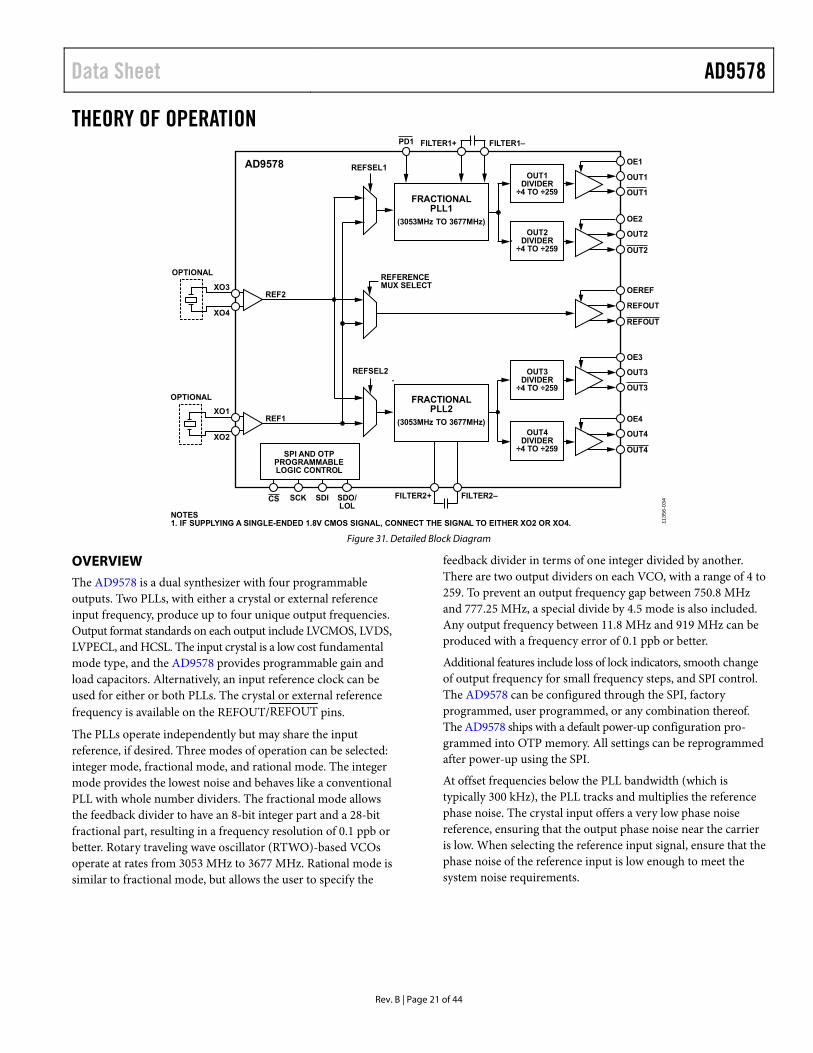
THEORY OF OPERATION
AD9578
FRACTIONALPLL2
(3053MHz TO 3677MHz)
FRACTIONALPLL1
(3053MHz TO 3677MHz)
OUT1DIVIDER
÷4 TO ÷259
OUT2DIVIDER
÷4 TO ÷259
OUT3DIVIDER
÷4 TO ÷259
OUT4DIVIDER
÷4 TO ÷259
REFOUT
REFOUT
OUT1
OUT1
OEREF
OE1
OUT2
OUT2
OE2
OUT3
OUT3
OE3
OUT4
OUT4
OE4
PD1
CS SCK SDI SDO/LOL
FILTER2+ FILTER2–
REFERENCEMUX SELECT
REFSEL2
REFSEL1
SPI AND OTPPROGRAMMABLELOGIC CONTROL
FILTER1+ FILTER1–
OPTIONAL
OPTIONAL
XO3
XO4
XO1
XO2
REF1
REF2
NOTES1. IF SUPPLYING A SINGLE-ENDED 1.8V CMOS SIGNAL, CONNECT THE SIGNAL TO EITHER XO2 OR XO4. 11
356-
034
Figure 31. Detailed Block Diagram
OVERVIEW The AD9578 is a dual synthesizer with four programmable outputs. Two PLLs, with either a crystal or external reference input frequency, produce up to four unique output frequencies. Output format standards on each output include LVCMOS, LVDS, LVPECL, and HCSL. The input crystal is a low cost fundamental mode type, and the AD9578 provides programmable gain and load capacitors. Alternatively, an input reference clock can be used for either or both PLLs. The crystal or external reference frequency is available on the REFOUT/REFOUT pins.
The PLLs operate independently but may share the input reference, if desired. Three modes of operation can be selected: integer mode, fractional mode, and rational mode. The integer mode provides the lowest noise and behaves like a conventional PLL with whole number dividers. The fractional mode allows the feedback divider to have an 8-bit integer part and a 28-bit fractional part, resulting in a frequency resolution of 0.1 ppb or better. Rotary traveling wave oscillator (RTWO)-based VCOs operate at rates from 3053 MHz to 3677 MHz. Rational mode is similar to fractional mode, but allows the user to specify the
feedback divider in terms of one integer divided by another. There are two output dividers on each VCO, with a range of 4 to 259. To prevent an output frequency gap between 750.8 MHz and 777.25 MHz, a special divide by 4.5 mode is also included. Any output frequency between 11.8 MHz and 919 MHz can be produced with a frequency error of 0.1 ppb or better.
Additional features include loss of lock indicators, smooth change of output frequency for small frequency steps, and SPI control. The AD9578 can be configured through the SPI, factory programmed, user programmed, or any combination thereof. The AD9578 ships with a default power-up configuration pro-grammed into OTP memory. All settings can be reprogrammed after power-up using the SPI.
At offset frequencies below the PLL bandwidth (which is typically 300 kHz), the PLL tracks and multiplies the reference phase noise. The crystal input offers a very low phase noise reference, ensuring that the output phase noise near the carrier is low. When selecting the reference input signal, ensure that the phase noise of the reference input is low enough to meet the system noise requirements.
AD9578 Data Sheet
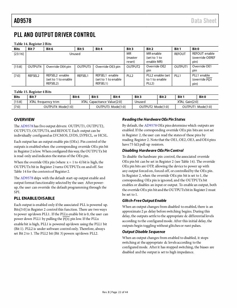
Rev. B | Page 22 of 44
PLL AND OUTPUT DRIVER CONTROL Table 14. Register 2 Bits Bits Bit 7 Bit 6 Bit 5 Bit 4 Bit 3 Bit 2 Bit 1 Bit 0
[23:16] Unused MR (master reset)
MR enable (set to 1 to enable MR)
REFOUT REFOUT enable (override OEREF pin)
[15:8] OUTPUT4 Override OE4 pin OUTPUT3 Override OE3 pin OUTPUT2 Override OE2 pin
OUTPUT1 Override OE1 pin
[7:0] REFSEL2 REFSEL2 enable (set to 1 to enable REFSEL2)
REFSEL1 REFSEL1 enable (set to 1 to enable REFSEL1)
PLL2 PLL2 enable (set to 1 to enable PLL2)
PLL1 PLL1 enable (override PD1 pin)
Table 15. Register 4 Bits Bits Bit 7 Bit 6 Bit 5 Bit 4 Bit 3 Bit 2 Bit 1 Bit 0
[15:8] XTAL frequency trim XTAL Capacitance Value[2:0] Unused XTAL Gain[2:0]
[7:0] OUTPUT4 Mode[1:0] OUTPUT3 Mode[1:0] OUTPUT2 Mode[1:0] OUTPUT1 Mode[1:0]
OVERVIEW The AD9578 has five output drivers: OUTPUT1, OUTPUT2, OUTPUT3, OUTPUT4, and REFOUT. Each output can be individually configured as LVCMOS, LVDS, LVPECL, or HCSL.
Each output has an output enable pin (OEx). Pin control of the outputs is enabled when the corresponding override OEx pin bit in Register 2 is low. When configured this way, the OUTPUTx bit is read only and indicates the status of the OEx pin.
When the override OEx pin (where x = 1 to 4) bit is high, the OUTPUTx bit in Register 2 turns OUTPUTx on and off. See Table 14 for the contents of Register 2.
The AD9578 ships with the default start-up output enable and output format functionality selected by the user. After power-up, the user can override the default programming through the SPI.
PLL ENABLE/DISABLE Each output is enabled only if the associated PLL is powered up. Bits[3:0] in Register 2 control this function. There are two ways to power up/down PLL1. If the PLLx enable bit is 0, the user can power down PLL1 by pulling the PD1 pin low. If the PLLx enable bit is high, PLL1 is powered up/down using the PLL1 bit (Bit 1). PLL2 is under software control only. Therefore, always set Bit 2 to 1. The PLL2 bit (Bit 3) powers up/down PLL2.
Reading the Hardware OEx Pin States
By default, the AD9578 OEx pins determine which outputs are enabled. If the corresponding override OEx pin bits are not set in Register 2, the user can read the states of these pins by reading Register 2. Note that the OE1, OE2, OE3, and OE4 pins have 75 kΩ pull-up resistors.
Disabling Hardware OEx Pin Control
To disable the hardware pin control, the associated override OEx pin bit can be set in Register 2 (see Table 14). The override OEx pin bits are OTP, allowing the device to power up with any output forced on, forced off, or controlled by the OEx pin. In Register 2, when the override OEx pin bit is set to 1, the corresponding OEx pin is ignored, and the OUTPUTx bit enables or disables an input or output. To enable an output, both the override OEx pin bit and the OUTPUTx bit in Register 2 must be set to 1.
Glitch-Free Output Enable
When an output changes from disabled to enabled, there is an approximate 2 µs delay before switching begins. During this delay, the outputs settle to the appropriate dc differential levels according to the configured mode. After this initial delay, the outputs begin toggling without glitches or runt pulses.
Output Disable Sequence
When an output changes from enabled to disabled, it stops switching at the appropriate dc levels according to the configured mode. After it has stopped switching, the biases are disabled and the output is set to high impedance.
Data Sheet AD9578
Rev. B | Page 23 of 44
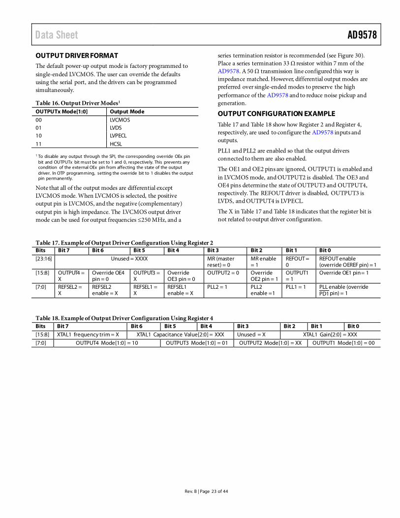
OUTPUT DRIVER FORMAT The default power-up output mode is factory programmed to single-ended LVCMOS. The user can override the defaults using the serial port, and the drivers can be programmed simultaneously.
Table 16. Output Driver Modes1 OUTPUTx Mode[1:0] Output Mode
00 LVCMOS 01 LVDS 10 LVPECL
11 HCSL
1 To disable any output through the SPI, the corresponding override OEx pin bit and OUTPUTx bit must be set to 1 and 0, respectively. This prevents any condition of the external OEx pin from affecting the state of the output driver. In OTP programming, setting the override bit to 1 disables the output pin permanently.
Note that all of the output modes are differential except LVCMOS mode. When LVCMOS is selected, the positive output pin is LVCMOS, and the negative (complementary) output pin is high impedance. The LVCMOS output driver mode can be used for output frequencies ≤250 MHz, and a
series termination resistor is recommended (see Figure 30). Place a series termination 33 Ω resistor within 7 mm of the AD9578. A 50 Ω transmission line configured this way is impedance matched. However, differential output modes are preferred over single-ended modes to preserve the high performance of the AD9578 and to reduce noise pickup and generation.
OUTPUT CONFIGURATION EXAMPLE Table 17 and Table 18 show how Register 2 and Register 4, respectively, are used to configure the AD9578 inputs and outputs.
PLL1 and PLL2 are enabled so that the output drivers connected to them are also enabled.
The OE1 and OE2 pins are ignored, OUTPUT1 is enabled and in LVCMOS mode, and OUTPUT2 is disabled. The OE3 and OE4 pins determine the state of OUTPUT3 and OUTPUT4, respectively. The REFOUT driver is disabled, OUTPUT3 is LVDS, and OUTPUT4 is LVPECL.
The X in Table 17 and Table 18 indicates that the register bit is not related to output driver configuration.
Table 17. Example of Output Driver Configuration Using Register 2 Bits Bit 7 Bit 6 Bit 5 Bit 4 Bit 3 Bit 2 Bit 1 Bit 0
[23:16] Unused = XXXX MR (master reset) = 0
MR enable = 1
REFOUT = 0
REFOUT enable (override OEREF pin) = 1
[15:8] OUTPUT4 = X
Override OE4 pin = 0
OUTPUT3 = X
Override OE3 pin = 0
OUTPUT2 = 0 Override OE2 pin = 1
OUTPUT1 = 1
Override OE1 pin = 1
[7:0] REFSEL2 = X
REFSEL2 enable = X
REFSEL1 = X
REFSEL1 enable = X
PLL2 = 1 PLL2 enable =1
PLL1 = 1 PLL enable (override PD1 pin) = 1
Table 18. Example of Output Driver Configuration Using Register 4 Bits Bit 7 Bit 6 Bit 5 Bit 4 Bit 3 Bit 2 Bit 1 Bit 0
[15:8] XTAL1 frequency trim = X XTAL1 Capacitance Value[2:0] = XXX Unused = X XTAL1 Gain[2:0] = XXX
[7:0] OUTPUT4 Mode[1:0] = 10 OUTPUT3 Mode[1:0] = 01 OUTPUT2 Mode[1:0] = XX OUTPUT1 Mode[1:0] = 00
AD9578 Data Sheet
Rev. B | Page 24 of 44
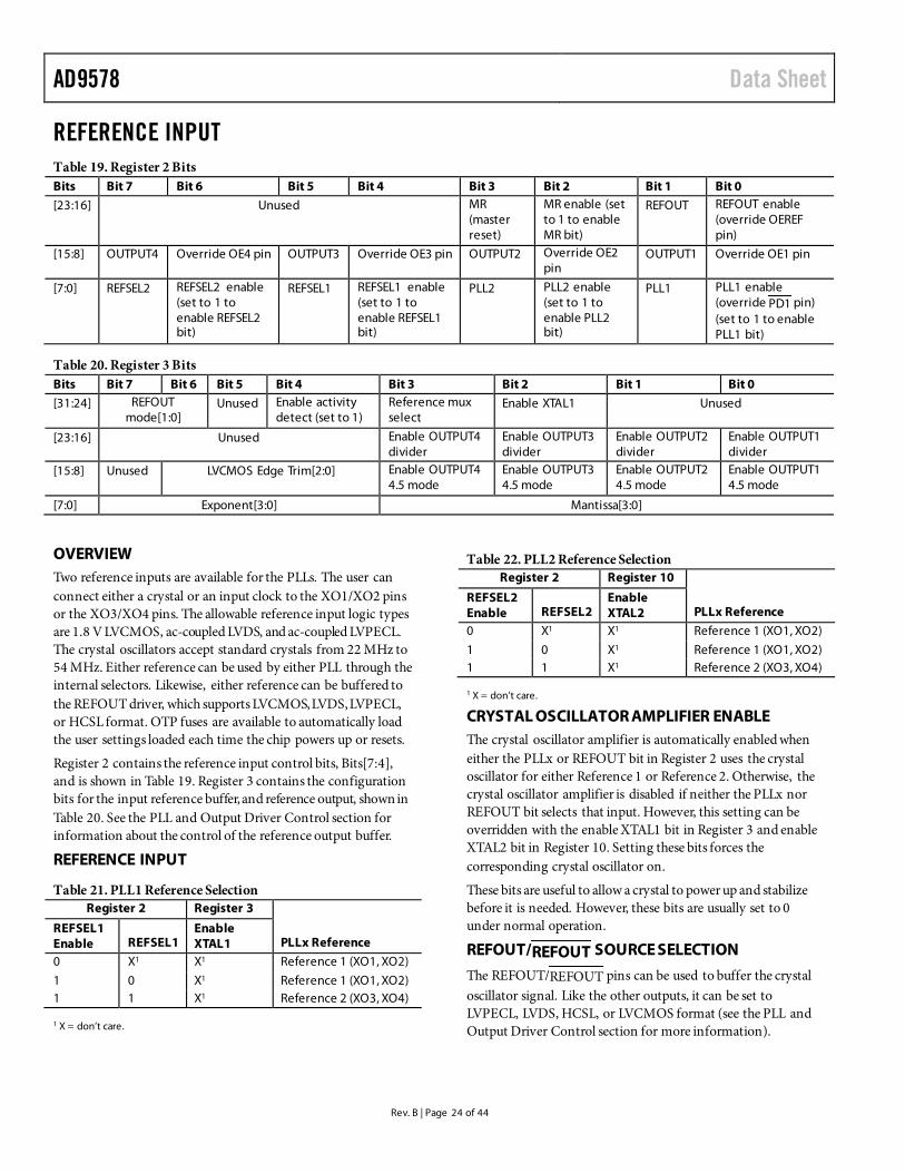
REFERENCE INPUT Table 19. Register 2 Bits Bits Bit 7 Bit 6 Bit 5 Bit 4 Bit 3 Bit 2 Bit 1 Bit 0
[23:16] Unused MR (master reset)
MR enable (set to 1 to enable MR bit)
REFOUT REFOUT enable (override OEREF pin)
[15:8] OUTPUT4 Override OE4 pin OUTPUT3 Override OE3 pin OUTPUT2 Override OE2 pin
OUTPUT1 Override OE1 pin
[7:0] REFSEL2 REFSEL2 enable (set to 1 to enable REFSEL2 bit)
REFSEL1 REFSEL1 enable (set to 1 to enable REFSEL1 bit)
PLL2 PLL2 enable (set to 1 to enable PLL2 bit)
PLL1 PLL1 enable (override PD1 pin) (set to 1 to enable PLL1 bit)
Table 20. Register 3 Bits Bits Bit 7 Bit 6 Bit 5 Bit 4 Bit 3 Bit 2 Bit 1 Bit 0
[31:24] REFOUT mode[1:0]
Unused Enable activity detect (set to 1)
Reference mux select
Enable XTAL1 Unused
[23:16] Unused Enable OUTPUT4 divider
Enable OUTPUT3 divider
Enable OUTPUT2 divider
Enable OUTPUT1 divider
[15:8] Unused LVCMOS Edge Trim[2:0] Enable OUTPUT4 4.5 mode
Enable OUTPUT3 4.5 mode
Enable OUTPUT2 4.5 mode
Enable OUTPUT1 4.5 mode
[7:0] Exponent[3:0] Mantissa[3:0]
OVERVIEW Two reference inputs are available for the PLLs. The user can connect either a crystal or an input clock to the XO1/XO2 pins or the XO3/XO4 pins. The allowable reference input logic types are 1.8 V LVCMOS, ac-coupled LVDS, and ac-coupled LVPECL. The crystal oscillators accept standard crystals from 22 MHz to 54 MHz. Either reference can be used by either PLL through the internal selectors. Likewise, either reference can be buffered to the REFOUT driver, which supports LVCMOS, LVDS, LVPECL, or HCSL format. OTP fuses are available to automatically load the user settings loaded each time the chip powers up or resets.
Register 2 contains the reference input control bits, Bits[7:4], and is shown in Table 19. Register 3 contains the configuration bits for the input reference buffer, and reference output, shown in Table 20. See the PLL and Output Driver Control section for information about the control of the reference output buffer.
REFERENCE INPUT
Table 21. PLL1 Reference Selection Register 2 Register 3
REFSEL1 Enable REFSEL1
Enable XTAL1 PLLx Reference
0 X1 X1 Reference 1 (XO1, XO2)
1 0 X1 Reference 1 (XO1, XO2) 1 1 X1 Reference 2 (XO3, XO4)
1 X = don’t care.
Table 22. PLL2 Reference Selection Register 2 Register 10
REFSEL2 Enable REFSEL2
Enable XTAL2 PLLx Reference
0 X1 X1 Reference 1 (XO1, XO2)
1 0 X1 Reference 1 (XO1, XO2) 1 1 X1 Reference 2 (XO3, XO4)
1 X = don’t care.
CRYSTAL OSCILLATOR AMPLIFIER ENABLE The crystal oscillator amplifier is automatically enabled when either the PLLx or REFOUT bit in Register 2 uses the crystal oscillator for either Reference 1 or Reference 2. Otherwise, the crystal oscillator amplifier is disabled if neither the PLLx nor REFOUT bit selects that input. However, this setting can be overridden with the enable XTAL1 bit in Register 3 and enable XTAL2 bit in Register 10. Setting these bits forces the corresponding crystal oscillator on.
These bits are useful to allow a crystal to power up and stabilize before it is needed. However, these bits are usually set to 0 under normal operation.
REFOUT/REFOUT SOURCE SELECTION
The REFOUT/REFOUT pins can be used to buffer the crystal oscillator signal. Like the other outputs, it can be set to LVPECL, LVDS, HCSL, or LVCMOS format (see the PLL and Output Driver Control section for more information).
Data Sheet AD9578
Rev. B | Page 25 of 44
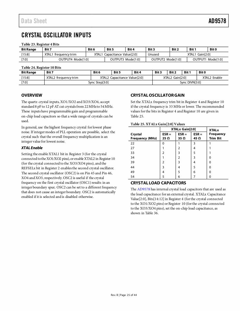
CRYSTAL OSCILLATOR INPUTS Table 23. Register 4 Bits Bit Range Bit 7 Bit 6 Bit 5 Bit 4 Bit 3 Bit 2 Bit 1 Bit 0
[15:8] XTAL1 frequency trim XTAL1 Capacitance Value[2:0] Unused XTAL1 Gain[2:0]
[7:0] OUTPUT4 Mode[1:0] OUTPUT3 Mode[1:0] OUTPUT2 Mode[1:0] OUTPUT1 Mode[1:0]
Table 24. Register 10 Bits Bit Range Bit 7 Bit 6 Bit 5 Bit 4 Bit 3 Bit 2 Bit 1 Bit 0
[15:8] XTAL2 frequency trim XTAL2 Capacitance Value[2:0] XTAL2 Gain[2:0] XTAL2 Enable [7:0] Sync Step[3:0] Sync DIVN[3:0]
OVERVIEW The quartz crystal inputs, XO1/XO2 and XO3/XO4, accept standard 8 pF to 12 pF AT cut crystals from 22 MHz to 54 MHz. These inputs have programmable gain and programmable on-chip load capacitors so that a wide range of crystals can be used.
In general, use the highest frequency crystal for lowest phase noise. If integer modes of PLL operation are possible, select the crystal such that the overall frequency multiplication is an integer value for lowest noise.
XTAL Enable
Setting the enable XTAL1 bit in Register 3 (for the crystal connected to the XO1/XO2 pins), or enable XTAL2 in Register 10 (for the crystal connected to the XO3/XO4 pins), and the REFSELx bit in Register 2 enables the second crystal oscillator. The second crystal oscillator (OSC2) is on Pin 45 and Pin 46, XO4 and XO3, respectively. OSC2 is useful if the crystal frequency on the first crystal oscillator (OSC1) results in an integer boundary spur; OSC2 can be set to a different frequency that does not cause an integer boundary. OSC2 is automatically enabled if it is selected and is disabled otherwise.
CRYSTAL OSCILLATOR GAIN Set the XTALx frequency trim bit in Register 4 and Register 10 if the crystal frequency is 33 MHz or lower. The recommended values for the bits in Register 4 and Register 10 are given in Table 25.
Table 25. XTALx Gain[2:0] Values
Crystal Frequency (MHz)
XTALx Gain[2:0] XTALx Frequency Trim Bit
ESR = 25 Ω
ESR = 35 Ω
ESR = 45 Ω
22 0 1 3 1 27 1 2 4 1 33 2 3 5 1 34 1 2 3 0 39 2 3 4 0
44 3 4 5 0 49 4 5 6 0 54 5 6 7 0
CRYSTAL LOAD CAPACITORS The AD9578 has internal crystal load capacitors that are used as the load capacitance for an external crystal. XTALx Capacitance Value[2:0], Bits[14:12] in Register 4 (for the crystal connected to the XO1/XO2 pins) or Register 10 (for the crystal connected to the XO3/XO4 pins), set the on-chip load capacitance, as shown in Table 36.
AD9578 Data Sheet
Rev. B | Page 26 of 44
PLLs OVERVIEW The two PLLs in the AD9578 operate independently. Each PLL consists of an input reference frequency (which can be shared), a phase/frequency detector, loop filter, RTWO-based VCO, complex feedback divider and phase selector, and two output dividers. The feedback divider can operate in two distinct modes: integer and fractional.
Using the AD9578 evaluation software is the easiest way to configure the AD9578. See the PLL Modes of Operation section for more information on the various register settings.
In the PLL Modes of Operation section, the possible feedback divider settings is expressed in Q notation, QN.M, where N (the integer part) is eight bits and M (the fractional part) is 28 bits.
The S[1:0] value represents the amount of phase interpolation used to represent a portion of the fractional part of the divider value. When S[1:0] = 3, there is no phase interpolation. When S[1:0] = 0, there is phase interpolation in 1/8 increments.
PLL MODES OF OPERATION The PLLs on the AD9578 have three modes of operation: integer, fractional, and rational. In this section, PLLx refers to either PLL1 (whose settings are in Register 6 and Register 7) or PLL2 (whose settings are Register 8 and Register 9).
The feedback divider has two parts: an 8-bit integer part and a 28-bit fractional part. The fractional part is modulated by a multistage noise shaping (MASH) modulator. The order of the MASH modulator is set in PLLx MASH[2:0] in Register 7 and Register 9, Bits[31:29].
Set the value of MASH[2:0] to 0 for integer mode, and 1 to 4 for fractional mode. Setting PLLx MASH[2:0] = 2 usually provides the lowest jitter for settings of PLLx Fractional Feedback Divider[27:0] greater than 2% from an integer. The value of S[1:0] is as follows: S[1:0] = 0, 1, and 2 results in eight, four, and two phases, respectively. Typically, a value of 0 for S[1:0] is best.
Fractional Mode
The fractional mode allows the feedback divider to take on a value of the Q notation, QN.M, where N (the integer part) is eight bits and M (the fractional part) is 28 bits. The VCO frequency divided by the feedback divider must always equal the reference frequency.
+×= 282
FRACINTff INVCO
where: INT is PLLx Integer Feedback Divider[7:0] in Register 6 (for PLL1) or Register 8 (for PLL2). FRAC is PLLx Fractional Feedback Divider[27:0] in Register 6 (for PLL1) or Register 8 (for PLL2)
Rational Mode
Rational mode allows the user to express the feedback divider as a ratio of rational numbers. Rational mode is enabled by setting the rational mode bit (Bit 2 in Register 7 (for PLL1) or Register 9 (for PLL2)) to 1.
Table 26. Rational Mode Feedback Divider Calculation
S[1:0] Feedback Divider (FBDIV)1
PLLx Fractional Feedback Divider[27:25]
S = 0 FBDIV = A + (1/8)(B + C/D) B = 0, 1, … , 7 (Bits[27:25]) S = 1 FBDIV = A + (1/4)(B + C/D) B = 0, 1, 2, 3 (Bits[27:26]) S = 2 FBDIV = A + (1/2)(B + C/D) B = 0, 1 (Bit 27) S = 3 FBDIV = A + C/D B ignored (Bits[27:25] =
000b) 1 A is PLLx Integer Feedback Divider[7:0], C is PLLx Fractional Feedback
Divider[24:9], D is PLLx Modulus Value[15:0].
Integer Mode
Integer mode provides the lowest possible phase noise and behaves like a traditional integer PLL in which the feedback divisor is an integer. Integer mode is a special case of rational mode in which the rational mode bit is zero, and the C and D terms in Table 26 are 0.
Integer mode is set when the following conditions are met:
• PLLx MASH[2:0] = 000b • PLLx Fractional Feedback Divider[24:0] = 0x000 • If PLLx S[1:0] = 3 (no phase interpolation),
PLLx Fractional Feedback Divider[27:25] must be zero. • If PLLx S[1:0] = 2 (phase interpolation of ½ or 0)
PLLx Fractional Feedback Divider[26:25] must be zero. • If PLLx S[1:0] = 1, (phase interpolation of 1/4, 1/2, 3/4, or 0)
PLLx Fractional Feedback Divider[25] must be zero.
When programming integer mode with S[1:0] = 0, the AD9578 is in integer mode (with better noise performance), even though the feedback divider has a fraction (for example, 1/8, 2/8, 3/8). When using this mode, the user must reset the feedback divider by writing a 1 to Bit 14 of Register 7 (for PLL1) or Register 9 (for PLL2).
NCO Functionality
Fractional mode allows operation as a precision NCO, which offers the capability of digitally pulling the output frequency using precise numerical control. A digital alternative to analog VCXOs that pull the crystal using varactors, NCO functionality enables completely digitally controlled PLLs that trim the output frequency through the fast SPI bus. Precise numerical control enables PLL applications to be implemented digitally within FPGAs and other digital ICs. Writing the AD9578 registers using an SPI bus that runs at 100 MHz allows the AD9578 output frequency to be updated frequently. The continuous trimming range of the output is greater than 1000 ppm, resulting
Data Sheet AD9578
Rev. B | Page 27 of 44
in better tracking range than is possible with analog VCXO-based PLLs.
The output frequencies change smoothly with no sudden phase step when the change to the feedback divider is small (for example, a change in phase or a few parts per million in frequency.) The change in the feedback divider is instantaneous, but the PLL response causes the PLL to change its frequency gradually. Thus, any changes small enough not to cause lock disturbance are smooth and continuous.
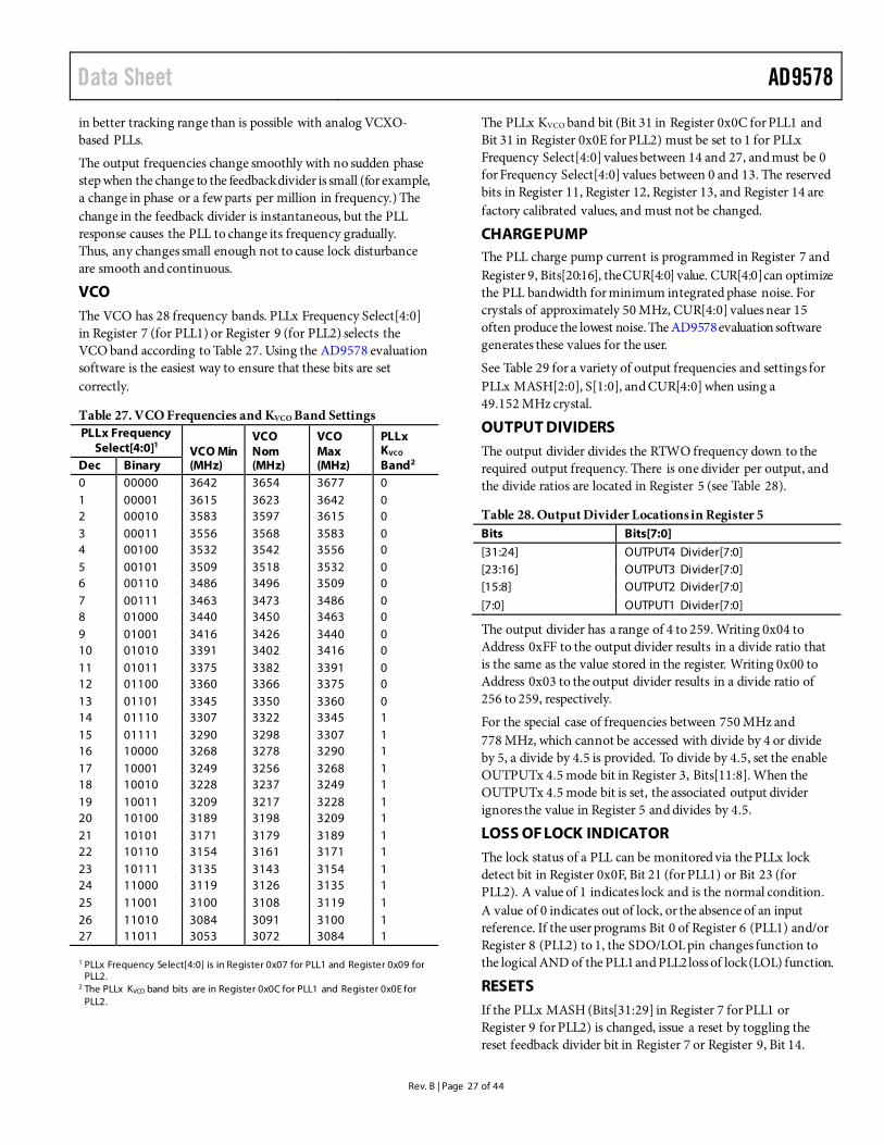
VCO The VCO has 28 frequency bands. PLLx Frequency Select[4:0] in Register 7 (for PLL1) or Register 9 (for PLL2) selects the VCO band according to Table 27. Using the AD9578 evaluation software is the easiest way to ensure that these bits are set correctly.
Table 27. VCO Frequencies and KVCO Band Settings PLLx Frequency
Select[4:0]1 VCO Min (MHz)
VCO Nom (MHz)
VCO Max (MHz)
PLLx KVCO Band2 Dec Binary
0 00000 3642 3654 3677 0 1 00001 3615 3623 3642 0 2 00010 3583 3597 3615 0 3 00011 3556 3568 3583 0 4 00100 3532 3542 3556 0 5 00101 3509 3518 3532 0 6 00110 3486 3496 3509 0 7 00111 3463 3473 3486 0 8 01000 3440 3450 3463 0 9 01001 3416 3426 3440 0 10 01010 3391 3402 3416 0 11 01011 3375 3382 3391 0 12 01100 3360 3366 3375 0 13 01101 3345 3350 3360 0 14 01110 3307 3322 3345 1 15 01111 3290 3298 3307 1 16 10000 3268 3278 3290 1 17 10001 3249 3256 3268 1 18 10010 3228 3237 3249 1 19 10011 3209 3217 3228 1 20 10100 3189 3198 3209 1 21 10101 3171 3179 3189 1 22 10110 3154 3161 3171 1 23 10111 3135 3143 3154 1 24 11000 3119 3126 3135 1 25 11001 3100 3108 3119 1 26 11010 3084 3091 3100 1 27 11011 3053 3072 3084 1
1 PLLx Frequency Select[4:0] is in Register 0x07 for PLL1 and Register 0x09 for PLL2.
2 The PLLx KVCO band bits are in Register 0x0C for PLL1 and Register 0x0E for PLL2.
The PLLx KVCO band bit (Bit 31 in Register 0x0C for PLL1 and Bit 31 in Register 0x0E for PLL2) must be set to 1 for PLLx Frequency Select[4:0] values between 14 and 27, and must be 0 for Frequency Select[4:0] values between 0 and 13. The reserved bits in Register 11, Register 12, Register 13, and Register 14 are factory calibrated values, and must not be changed.
CHARGE PUMP The PLL charge pump current is programmed in Register 7 and Register 9, Bits[20:16], the CUR[4:0] value. CUR[4:0] can optimize the PLL bandwidth for minimum integrated phase noise. For crystals of approximately 50 MHz, CUR[4:0] values near 15 often produce the lowest noise. The AD9578 evaluation software generates these values for the user.
See Table 29 for a variety of output frequencies and settings for PLLx MASH[2:0], S[1:0], and CUR[4:0] when using a 49.152 MHz crystal.
OUTPUT DIVIDERS The output divider divides the RTWO frequency down to the required output frequency. There is one divider per output, and the divide ratios are located in Register 5 (see Table 28).
Table 28. Output Divider Locations in Register 5 Bits Bits[7:0]
[31:24] OUTPUT4 Divider[7:0] [23:16] OUTPUT3 Divider[7:0] [15:8] OUTPUT2 Divider[7:0]
[7:0] OUTPUT1 Divider[7:0]
The output divider has a range of 4 to 259. Writing 0x04 to Address 0xFF to the output divider results in a divide ratio that is the same as the value stored in the register. Writing 0x00 to Address 0x03 to the output divider results in a divide ratio of 256 to 259, respectively.
For the special case of frequencies between 750 MHz and 778 MHz, which cannot be accessed with divide by 4 or divide by 5, a divide by 4.5 is provided. To divide by 4.5, set the enable OUTPUTx 4.5 mode bit in Register 3, Bits[11:8]. When the OUTPUTx 4.5 mode bit is set, the associated output divider ignores the value in Register 5 and divides by 4.5.
LOSS OF LOCK INDICATOR The lock status of a PLL can be monitored via the PLLx lock detect bit in Register 0x0F, Bit 21 (for PLL1) or Bit 23 (for PLL2). A value of 1 indicates lock and is the normal condition. A value of 0 indicates out of lock, or the absence of an input reference. If the user programs Bit 0 of Register 6 (PLL1) and/or Register 8 (PLL2) to 1, the SDO/LOL pin changes function to the logical AND of the PLL1 and PLL2 loss of lock (LOL) function.
RESETS If the PLLx MASH (Bits[31:29] in Register 7 for PLL1 or Register 9 for PLL2) is changed, issue a reset by toggling the reset feedback divider bit in Register 7 or Register 9, Bit 14.
AD9578 Data Sheet
Rev. B | Page 28 of 44
EXAMPLE VALUES FOR 49.152 MHZ CRYSTAL Table 29 shows the output frequency settings when using a 49.152 MHz crystal, TXC Part Number 8Z49100001, 2.5 mm × 2.0 mm, 49.152 MHz, ±30 ppm, CL = 9 pF, maximum ESR = 50 Ω.
Table 29. Register Settings for Various Output Frequencies with a 49.152 MHz Crystal Output Frequency (MHz)
PLLx Feedback Divider
OUTPUTx Divider[7:0]
Frequency Select[4:0]
PLLx KVCO Band
PLLx MASH[2:0] S[1:0] CUR[4:0]
VCO Frequency (MHz)
125.000000 71.207682292 28 6 0 2 0 17 3500
155.520000 69.609375 22 9 0 2 0 16 3421.44 156.250000 66.757202148 21 16 1 2 0 16 3281.25 159.375000 68.092346191 21 13 0 2 0 16 3346.875 161.132813 72.121620402 22 4 0 2 0 16 3544.92189
164.355469 70.220232117 21 8 0 2 0 19 3451.46485 166.628571 74.581473023 22 0 0 2 0 19 3665.82856 167.331646 68.087421061 20 13 0 2 0 19 3346.63292 168.040678 71.79472327 21 5 0 2 0 15 3528.85424 172.642299 73.760747864 21 1 0 2 0 19 3625.48828
173.370748 74.071974854 21 1 0 2 0 22 3640.78571 174.105369 74.385838806 21 0 0 2 0 19 3656.21275 174.153733 70.863335368 20 7 0 2 0 19 3483.07466 174.703084 71.086866862 20 6 0 2 0 16 3494.06168
176.095145 71.653297933 20 5 0 2 0 15 3521.9029 176.838163 64.760069458 18 21 1 2 0 15 3183.08693 212.500000 69.173177083 16 10 0 2 0 14 3400 425.000000 69.173177083 8 10 0 2 0 14 3400 622.080000 63.281250000 5 25 1 2 0 16 3110.4
625.000000 63.57828776 5 24 1 2 0 14 3125 637.500000 64.849853516 5 21 1 2 0 13 3187.5 644.531250 65.565109253 5 19 1 2 0 12 3222.65625 657.421875 66.876411438 5 16 1 2 0 7 3287.10938
666.514286 67.801339315 5 14 1 3 0 15 3332.57143 669.326582 68.087420858 5 13 0 2 0 19 3346.63291 672.162712 68.375926921 5 12 0 2 0 9 3360.81356 690.569196 70.248331299 5 8 0 3 0 15 3452.84598 693.482991 70.544737854 5 7 0 2 0 12 3467.41495
696.421478 63.759290588 4.5 24 1 2 0 16 3133.89665 696.614931 70.863335266 5 7 0 2 0 19 3483.07465 698.812335 71.086866760 5 6 0 2 0 18 3494.06167 704.380580 71.653297933 5 5 0 2 0 15 3521.9029
707.352650 64.760069275 4.5 21 1 2 0 15 3183.08693
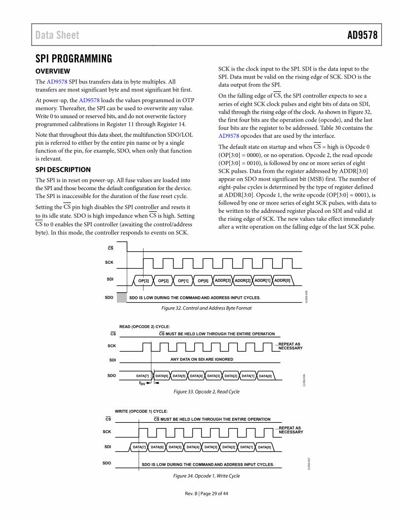
Data Sheet AD9578
Rev. B | Page 29 of 44
SPI PROGRAMMING OVERVIEW The AD9578 SPI bus transfers data in byte multiples. All transfers are most significant byte and most significant bit first.
At power-up, the AD9578 loads the values programmed in OTP memory. Thereafter, the SPI can be used to overwrite any value. Write 0 to unused or reserved bits, and do not overwrite factory programmed calibrations in Register 11 through Register 14.
Note that throughout this data sheet, the multifunction SDO/LOL pin is referred to either by the entire pin name or by a single function of the pin, for example, SDO, when only that function is relevant.
SPI DESCRIPTION The SPI is in reset on power-up. All fuse values are loaded into the SPI and those become the default configuration for the device. The SPI is inaccessible for the duration of the fuse reset cycle.
Setting the CS pin high disables the SPI controller and resets it to its idle state. SDO is high impedance when CS is high. Setting CS to 0 enables the SPI controller (awaiting the control/address byte). In this mode, the controller responds to events on SCK.
SCK is the clock input to the SPI. SDI is the data input to the SPI. Data must be valid on the rising edge of SCK. SDO is the data output from the SPI.
On the falling edge of CS, the SPI controller expects to see a series of eight SCK clock pulses and eight bits of data on SDI, valid through the rising edge of the clock. As shown in Figure 32, the first four bits are the operation code (opcode), and the last four bits are the register to be addressed. Table 30 contains the AD9578 opcodes that are used by the interface.
The default state on startup and when CS = high is Opcode 0 (OP[3:0] = 0000), or no operation. Opcode 2, the read opcode (OP[3:0] = 0010), is followed by one or more series of eight SCK pulses. Data from the register addressed by ADDR[3:0] appear on SDO most significant bit (MSB) first. The number of eight-pulse cycles is determined by the type of register defined at ADDR[3:0]. Opcode 1, the write opcode (OP[3:0] = 0001), is followed by one or more series of eight SCK pulses, with data to be written to the addressed register placed on SDI and valid at the rising edge of SCK. The new values take effect immediately after a write operation on the falling edge of the last SCK pulse.
CS
SCK
SDI
SDO
OP[2] OP[1] OP[0] ADDR[3] ADDR[2] ADDR[1] ADDR[0]
SDO IS LOW DURING THE COMMAND AND ADDRESS INPUT CYCLES.
OP[3]
1135
6-03
5
Figure 32. Control and Address Byte Format
CS
SCK
SDI
SDO
CS MUST BE HELD LOW THROUGH THE ENTIRE OPERATION
tDV
ANY DATA ON SDI ARE IGNORED
...REPEAT AS NECESSARY
READ (OPCODE 2) CYCLE:
DATA[0]DATA[7] DATA[6] DATA[5] DATA[4] DATA[3] DATA[2] DATA[1]
1135
6-03
6
Figure 33. Opcode 2, Read Cycle
...REPEAT AS NECESSARY
WRITE (OPCODE 1) CYCLE:
CS
SCK
SDI
SDO
CS MUST BE HELD LOW THROUGH THE ENTIRE OPERATION
SDO IS LOW DURING THE COMMAND AND ADDRESS INPUT CYCLES.
DATA[0]DATA[6] DATA[5] DATA[4] DATA[3] DATA[2] DATA[1]DATA[7]
1135
6-03
7
Figure 34. Opcode 1, Write Cycle
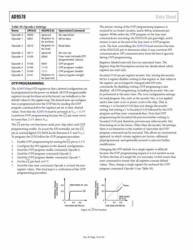
AD9578 Data Sheet
Rev. B | Page 30 of 44
Table 30. Opcode x Settings Name OP[3:0] ADDR[3:0] Operation/Command
Opcode 0 0000 Ignored No operation Opcode 1 0001 Register to
be written Write data
Opcode 2 0010 Register to be read
Read data
Opcode 3 0011 Ignored Do not use Opcode 4 0100 0000 Fuse reset (reloads OTP
programmed values)
Opcode 5 0100 0001 OTP program Opcode 6 0100 1110 OTP program enable Opcode 7 0100 1111 OTP program disable Opcode 8 0101 Register to
be queried Query register length
OTP PROGRAMMING The AD9578 has OTP registers so that a desired configuration can be programmed as the power-on default. All OTP programmable registers (except for those set at the factory) are initially set to the default values in the register map. The desired start-up configura-tion is programmed into the OTP bits by sending the OTP program command after the registers are set to their desired values. Note that the AD9578 must be powered at VDD = 3.3 V to perform OTP programming because the CS pin must never be more than 2.5 V above VDD.
The CS pin has two functions: serial port chip select and OTP programming enable. To access the SPI normally, use the CS pin at normal digital LVCMOS levels (between 0 V and VDD.) To program the OTP, follow the OTP program procedure:
1. Enable OTP programming by setting the CS pin to 5.5 V. 2. Configure the SPI registers to the desired configuration. 3. Send the OTP program enable command, Opcode 6. 4. Send the OTP program command, Opcode 5. 5. Send the OTP program disable command, Opcode 7. 6. Set the CS pin back to 0 V. 7. Send the fuse reset command, Opcode 4, to load the new
register values. This final step is a verification of the OTP programming procedure.
The precise timing of the OTP programming sequence is ensured by on-board circuitry, and is 800 μs minimum per register. While either the OTP program or the fuse reset commands are executing, the SDO/LOL pin goes high, and it returns to zero at the end of the fuse reset or OTP program cycle. The host controlling the AD9578 must monitor the state of the SDO/LOL pin to determine when it may continue SPI communication. SPI communication from the host is ignored during OTP programming.
Registers labeled read only have no associated fuses. The Register Map Bit Descriptions section has details about which registers are read only.
Security[15:0] are per register security bits. Setting the security bit for a register disables writing to that register so that values in the register can no longer be changed with SPI write commands. By disabling writing, OTP programing is also disabled. All OTP programing, including the security bits, can be performed at the same time. The new configuration settings for read/program bits, such as the security bits, is not applied until a fuse reset cycle or power cycle to the chip. That is, writing a 1 to Security[15:0] does not change the security setting, but writing a 1 to Security[15:0] followed by the OTP program and fuse reset commands does. Note that OTP programming the Security0 bit prevents further writing to Security[15:0] and, therefore, prevents any other security bits from being set in the future. Other than the security bit settings, there is no limitation to the number of times that the OTP program command can be executed. This allows an incremental approach in which certain registers are factory calibrated, preprogrammed, and optionally secured to prevent further modification.
Changing the OTP default for a single register is difficult because the OTP programming sequence is not random access. To blow the fuse of a single bit, it is necessary to first send a fuse reset command to ensure that all registers contain default values. Then, change a single register bit and send the OTP program command, Opcode 5 (see Table 30).
TRIP POINT AT 1.6V
TRIP POINTAT 4.1V
CS
INTE
RN
AL
SIG
NA
LVO
LTA
GE
(V)
VOLTAGE ON PIN (V)
5.0
5.0
3.3
3.300
VPROG
INTE
RN
AL
SIG
NA
LVO
LTA
GE
(V)
VOLTAGE ON PIN (V)
5.0
5.0
3.3
3.300
1135
6-03
9
Figure 35. CS Pin Function
Data Sheet AD9578
Rev. B | Page 31 of 44
SPI Configuration
The AD9578 can be programmed after power-up through the SPI. This section describes how to set a specific configuration in the SPI registers.
1. Prepare default values. The AD9578 evaluation software is an ideal way to determine the optimal default values of the AD9578 registers. Note that Register 0 and Register 1 are read only and cannot be changed.
2. Enable all subsystems. This normally includes the per PLL values found in Register 0x06 (for PLL1) and Register 0x08 (for PLL2). They are the feedback divider PU (Bit 1), VCO PU (Bit 2), and ENPFD (Bit 3), as well as the enable activity detect bit, which is a global bit (Register 0x03, Bit 28).
3. The enable XTAL1 (in Register 3) and enable XTAL2 (in Register 10) bits are normally set to 0 because the crystals
are enabled as necessary. Setting these to 1 forces the corresponding input on permanently.
4. The following bits are internal resets, and cannot be OTP programmed. These bits are in three groups (global, PLL1, and PLL2) and must be 0 for normal device operation. The internal reset global bits are in Register 15. The PLL1 bits are in Register 7, Bits[11:15]. The PLL2 bits are in Register 9, Bits[11:15].
5. For each output to be used (OUTPUT1 through OUTPUT4 and REFOUT), select the mode according to Table 16, as well as the corresponding enable bits in Register 2 and Register 3.
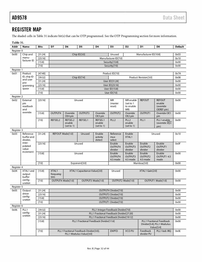
AD9578 Data Sheet
Rev. B | Page 32 of 44
REGISTER MAP The shaded cells in Table 31 indicate bit(s) that can be OTP programmed. See the OTP Programming section for more information.
Table 31. Addr Name Bits D7 D6 D5 D4 D3 D2 D1 D0 Default
Register 0 0x00 Chip and
manu-facturer ID
[31:24] Chip ID[3:0] Unused Manufacturer ID[10:8] 0x03
[23:16] Manufacturer ID[7:0] 0x10 [15:8] Security[15:8] 0x00 [7:0] Security[7:0] 0x00
Register 1 0x01 Product
ID, chip ID and user pro-gramming space
[47:40] Product ID[7:0] 0x7A
[39:32] Chip ID[7:4] Product Revision[3:0] 0x08 [31:24] User ID[31:24] 0x00
[23:16] User ID[23:16] 0x00 [15:8] User ID[15:8] 0x00
[7:0] User ID[7:0] 0x00 Register 2 0x02 External
pin readback and override
[23:16] Unused MR (master reset)
MR enable (set to 1 to enable MR)
REFOUT REFOUT enable (override OEREF pin)
0x00
[15:8] OUTPUT4 Override OE4 pin
OUTPUT3 Override OE3 pin
OUTPUT2 Override OE2 pin
OUTPUT1 Override OE1 pin
0x00
[7:0] REFSEL2 REFSEL2 enable (set to 1)
REFSEL1 REFSEL1 enable (set to 1)
PLL2 PLL2 enable (set to 1)
PLL1 PLL1 enable (override PD1 pin)
0x00
Register 3 0x03 Reference
buffer and divider, inter-polated value increment
[31:24] REFOUT Mode[1:0] Unused Enable activity detect
Reference mux select
Enable XTAL1
Unused 0x10
[23:16] Unused Enable OUTPUT4 divider
Enable OUTPUT3 divider
Enable OUTPUT2 divider
Enable OUTPUT1 divider
0x0F
[15:8] Unused Enable OUTPUT4 4.5 mode
Enable OUTPUT3 4.5 mode
Enable OUTPUT2 4.5 mode
Enable OUTPUT1 4.5 mode
0x00
[7:0] Exponent[3:0] Mantissa[3:0] 0x00
Register 4 0x04 XTAL1 and
output buffer config-uration
[15:8] XTAL1 frequency trim
XTAL1 Capacitance Value[2:0] Unused XTAL1 Gain[2:0] 0x00
[7:0] OUTPUT4 Mode[1:0] OUTPUT3 Mode[1:0] OUTPUT2 Mode[1:0] OUTPUT1 Mode[1:0] 0x00
Register 5 0x05 Output
driver config-uration
[31:24] OUTPUT4 Divider[7:0] 0x00
[23:16] OUTPUT3 Divider[7:0] 0x00 [15:8] OUTPUT2 Divider[7:0] 0x00
[7:0] OUTPUT1 Divider[7:0] 0x00 Register 6
0x06 PLL1 config-uration
[39:32] PLL1 Integer Feedback Divider[7:0] 0x00 [31:24] PLL1 Fractional Feedback Divider[27:20] 0x00 [23:16] PLL1 Fractional Feedback Divider[19:12] 0x00
[15:8] PLL1 Fractional Feedback Divider[11:6] PLL1 Fractional Feedback Divider[5:4]; PLL1 Modulus
Value[5:4]
0x00
[7:0] PLL1 Fractional Feedback Divider[3:0]; PLL1 Modulus Value[3:0]
ENPFD VCO PU Feedback divider PU
PLL1 lock IRQ 0x0E
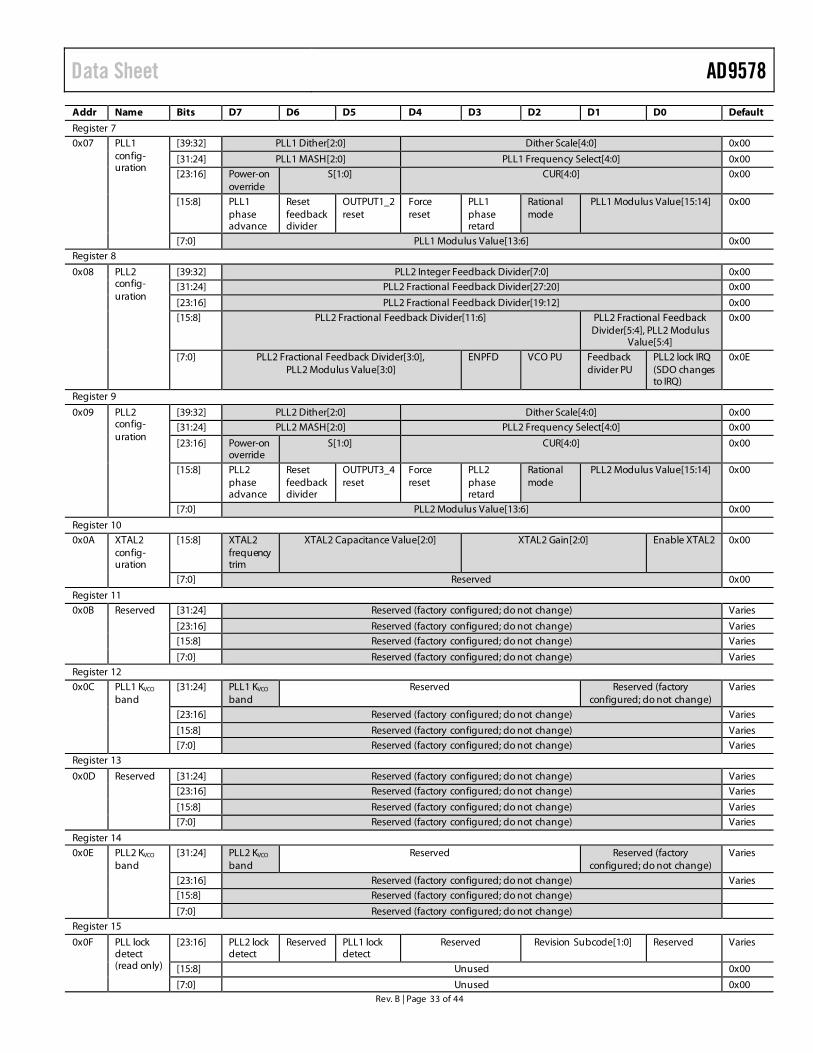
Data Sheet AD9578
Rev. B | Page 33 of 44
Addr Name Bits D7 D6 D5 D4 D3 D2 D1 D0 Default
Register 7 0x07 PLL1
config-uration
[39:32] PLL1 Dither[2:0] Dither Scale[4:0] 0x00
[31:24] PLL1 MASH[2:0] PLL1 Frequency Select[4:0] 0x00 [23:16] Power-on
override S[1:0] CUR[4:0] 0x00
[15:8] PLL1 phase advance
Reset feedback divider
OUTPUT1_2 reset
Force reset
PLL1 phase retard
Rational mode
PLL1 Modulus Value[15:14] 0x00
[7:0] PLL1 Modulus Value[13:6] 0x00 Register 8
0x08 PLL2 config-uration
[39:32] PLL2 Integer Feedback Divider[7:0] 0x00 [31:24] PLL2 Fractional Feedback Divider[27:20] 0x00
[23:16] PLL2 Fractional Feedback Divider[19:12] 0x00 [15:8] PLL2 Fractional Feedback Divider[11:6] PLL2 Fractional Feedback
Divider[5:4], PLL2 Modulus Value[5:4]
0x00
[7:0] PLL2 Fractional Feedback Divider[3:0], PLL2 Modulus Value[3:0]
ENPFD VCO PU Feedback divider PU
PLL2 lock IRQ (SDO changes to IRQ)
0x0E
Register 9
0x09 PLL2 config-uration
[39:32] PLL2 Dither[2:0] Dither Scale[4:0] 0x00 [31:24] PLL2 MASH[2:0] PLL2 Frequency Select[4:0] 0x00
[23:16] Power-on override
S[1:0] CUR[4:0] 0x00
[15:8] PLL2 phase advance
Reset feedback divider
OUTPUT3_4 reset
Force reset
PLL2 phase retard
Rational mode
PLL2 Modulus Value[15:14] 0x00
[7:0] PLL2 Modulus Value[13:6] 0x00
Register 10 0x0A XTAL2
config-uration
[15:8] XTAL2 frequency trim
XTAL2 Capacitance Value[2:0] XTAL2 Gain[2:0] Enable XTAL2 0x00
[7:0] Reserved 0x00
Register 11 0x0B Reserved [31:24] Reserved (factory configured; do not change) Varies
[23:16] Reserved (factory configured; do not change) Varies [15:8] Reserved (factory configured; do not change) Varies
[7:0] Reserved (factory configured; do not change) Varies Register 12 0x0C PLL1 KVCO
band [31:24] PLL1 KVCO
band Reserved Reserved (factory
configured; do not change) Varies
[23:16] Reserved (factory configured; do not change) Varies
[15:8] Reserved (factory configured; do not change) Varies [7:0] Reserved (factory configured; do not change) Varies
Register 13
0x0D Reserved [31:24] Reserved (factory configured; do not change) Varies [23:16] Reserved (factory configured; do not change) Varies
[15:8] Reserved (factory configured; do not change) Varies [7:0] Reserved (factory configured; do not change) Varies
Register 14 0x0E PLL2 KVCO
band [31:24] PLL2 KVCO
band Reserved Reserved (factory
configured; do not change) Varies
[23:16] Reserved (factory configured; do not change) Varies [15:8] Reserved (factory configured; do not change)
[7:0] Reserved (factory configured; do not change) Register 15
0x0F PLL lock detect (read only)
[23:16] PLL2 lock detect
Reserved PLL1 lock detect
Reserved Revision Subcode[1:0] Reserved Varies
[15:8] Unused 0x00
[7:0] Unused 0x00
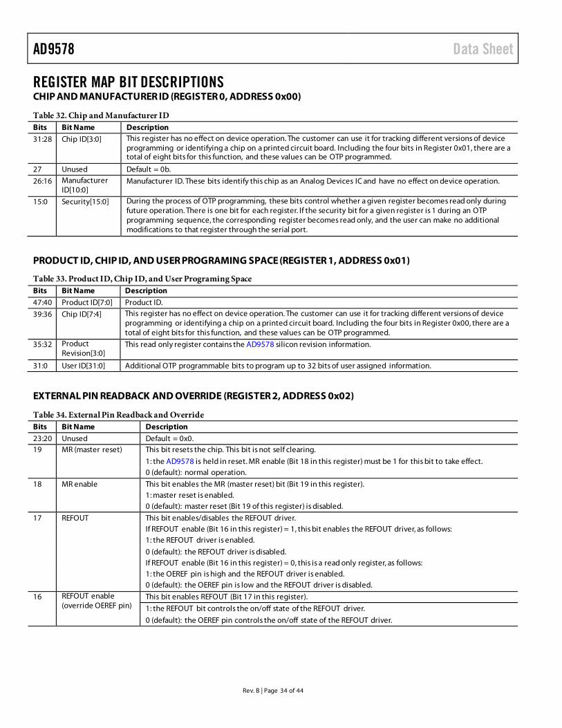
AD9578 Data Sheet
Rev. B | Page 34 of 44
REGISTER MAP BIT DESCRIPTIONS CHIP AND MANUFACTURER ID (REGISTER 0, ADDRESS 0x00)
Table 32. Chip and Manufacturer ID Bits Bit Name Description
31:28 Chip ID[3:0] This register has no effect on device operation. The customer can use it for tracking different versions of device programming or identifying a chip on a printed circuit board. Including the four bits in Register 0x01, there are a total of eight bits for this function, and these values can be OTP programmed.
27 Unused Default = 0b.
26:16 Manufacturer ID[10:0]
Manufacturer ID. These bits identify this chip as an Analog Devices IC and have no effect on device operation.
15:0 Security[15:0] During the process of OTP programming, these bits control whether a given register becomes read only during future operation. There is one bit for each register. If the security bit for a given register is 1 during an OTP programming sequence, the corresponding register becomes read only, and the user can make no additional modifications to that register through the serial port.
PRODUCT ID, CHIP ID, AND USER PROGRAMING SPACE (REGISTER 1, ADDRESS 0x01)
Table 33. Product ID, Chip ID, and User Programing Space Bits Bit Name Description
47:40 Product ID[7:0] Product ID.
39:36 Chip ID[7:4] This register has no effect on device operation. The customer can use it for tracking different versions of device programming or identifying a chip on a printed circuit board. Including the four bits in Register 0x00, there are a total of eight bits for this function, and these values can be OTP programmed.
35:32 Product Revision[3:0]
This read only register contains the AD9578 silicon revision information.
31:0 User ID[31:0] Additional OTP programmable bits to program up to 32 bits of user assigned information.
EXTERNAL PIN READBACK AND OVERRIDE (REGISTER 2, ADDRESS 0x02)
Table 34. External Pin Readback and Override Bits Bit Name Description
23:20 Unused Default = 0x0. 19 MR (master reset) This bit resets the chip. This bit is not self clearing.
1: the AD9578 is held in reset. MR enable (Bit 18 in this register) must be 1 for this bit to take effect. 0 (default): normal operation.
18 MR enable This bit enables the MR (master reset) bit (Bit 19 in this register). 1: master reset is enabled. 0 (default): master reset (Bit 19 of this register) is disabled.
17 REFOUT This bit enables/disables the REFOUT driver. If REFOUT enable (Bit 16 in this register) = 1, this bit enables the REFOUT driver, as follows: 1: the REFOUT driver is enabled.
0 (default): the REFOUT driver is disabled. If REFOUT enable (Bit 16 in this register) = 0, this is a read only register, as follows: 1: the OEREF pin is high and the REFOUT driver is enabled. 0 (default): the OEREF pin is low and the REFOUT driver is disabled.
16 REFOUT enable (override OEREF pin)
This bit enables REFOUT (Bit 17 in this register).
1: the REFOUT bit controls the on/off state of the REFOUT driver.
0 (default): the OEREF pin controls the on/off state of the REFOUT driver.
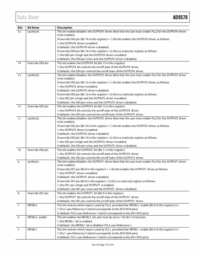
Data Sheet AD9578
Rev. B | Page 35 of 44
Bits Bit Name Description
15 OUTPUT4 This bit enables/disables the OUTPUT4 driver. Note that the user must enable PLL2 for the OUTPUT4 driver to be enabled.
If override OE4 pin (Bit 14 in this register) = 1, this bit enables the OUTPUT4 driver, as follows:
1: the OUTPUT4 driver is enabled. 0 (default): the OUTPUT4 driver is disabled. If override OE4 pin (Bit 14 in this register) = 0, this is a read only register, as follows: 1: the OE4 pin is high and the OUTPUT4 driver is enabled. 0 (default): the OE4 pin is low and the OUTPUT4 driver is disabled.
14 Override OE4 pin This bit enables the OUTPUT4 bit (Bit 15 in this register). 1: the OUTPUT4 bit controls the on/off state of the OUTPUT4 driver.
0 (default): the OE4 pin controls the on/off state of the OUTPUT4 driver.
13 OUTPUT3 This bit enables/disables the OUTPUT3 driver. Note that the user must enable PLL2 for the OUTPUT3 driver to be enabled.
If override OE3 pin (Bit 12 in this register) = 1, this bit enables the OUTPUT3 driver, as follows:
1: the OUTPUT3 driver is enabled. 0 (default): the OUTPUT3 driver is disabled. If override OE3 pin (Bit 12 in this register) = 0, this is a read only register, as follows: 1: the OE3 pin is high and the OUTPUT3 driver is enabled.
0 (default): the OE3 pin is low and the OUTPUT3 driver is disabled. 12 Override OE3 pin This bit enables the OUTPUT3 bit (Bit 13 in this register).
1: the OUTPUT3 bit controls the on/off state of the OUTPUT3 driver. 0 (default): the OE3 pin controls the on/off state of the OUTPUT3 driver.
11 OUTPUT2 This bit enables/disables the OUTPUT2 driver. Note that the user must enable PLL2 for the OUTPUT2 driver to be enabled.
If override OE2 pin (Bit 10 in this register) = 1, this bit enables the OUTPUT2 driver, as follows: 1: the OUTPUT2 driver is enabled. 0 (default): the OUTPUT2 driver is disabled. If override OE2 pin (Bit 10 in this register) = 0, this is a read only register, as follows:
1: the OE2 pin is high and the OUTPUT2 driver is enabled. 0 (default): the OE2 pin is low and the OUTPUT2 driver is disabled.
10 Override OE2 pin This bit enables the OUTPUT2 bit (Bit 11 in this register). 1: the OUTPUT2 bit controls the on/off state of the OUTPUT2 driver. 0 (default): the OE2 pin controls the on/off state of the OUTPUT2 driver.
9 OUTPUT1 This bit enables/disables the OUTPUT1 driver. Note that the user must enable PLL2 for the OUTPUT1 driver to be enabled.
If override OE1 pin (Bit 8 in this register) = 1, this bit enables the OUTPUT1 driver, as follows: 1: the OUTPUT1 driver is enabled. 0 (default): the OUTPUT1 driver is disabled.
If override OE1 pin (Bit 8 in this register) = 0, this is a read only register, as follows: 1: the OE1 pin is high and OUTPUT1 is enabled. 0 (default): the OE1 pin is low and the OUTPUT1 driver is disabled.
8 Override OE1 pin This bit enables the OUTPUT1 bit (Bit 9 in this register). 1: the OUTPUT1 bit controls the on/off state of the OUTPUT1 driver. 0 (default): the OE1 pin controls the on/off state of the OUTPUT1 driver.
7 REFSEL2 This bit controls which input is used by PLL2, provided that REFSEL2 enable (Bit 6 of this register) is 1. 1: PLL2 uses Reference 2 (which corresponds to the XO3/XO4 pins).
0: (default) PLL2 uses Reference 1 (which corresponds to the XO1/XO2 pins). 6 REFSEL2 enable This bit enables the REFSEL2 bit, and must be set to 1 for Bit 7 to function.
1: the REFSEL1 bit is enabled. 0 (default): the REFSEL1 bit is disabled. PLL2 uses Reference 1.
5 REFSEL1 This bit controls which input is used by PLL1, provided that REFSEL1 enable (Bit 4 of this register) is 1. 1: PLL1 uses Reference 2 (which corresponds to the XO3/XO4 pins). 0 (default): PLL1 uses Reference 1 (which corresponds to the XO1/XO2 pins).
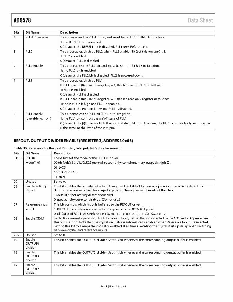
AD9578 Data Sheet
Rev. B | Page 36 of 44
Bits Bit Name Description
4 REFSEL1 enable This bit enables the REFSEL1 bit, and must be set to 1 for Bit 5 to function.
1: the REFSEL1 bit is enabled. 0 (default): the REFSEL1 bit is disabled. PLL1 uses Reference 1.
3 PLL2 This bit enables/disables PLL2 when PLL2 enable (Bit 2 of this register) is 1. 1: PLL2 is enabled. 0 (default): PLL2 is disabled.
2 PLL2 enable This bit enables the PLL2 bit, and must be set to 1 for Bit 3 to function.
1: the PLL2 bit is enabled.
0 (default): the PLL2 bit is disabled. PLL2 is powered down.
1 PLL1 This bit enables/disables PLL1. If PLL1 enable (Bit 0 in this register) = 1, this bit enables PLL1, as follows: 1: PLL1 is enabled. 0 (default): PLL1 is disabled. If PLL1 enable (Bit 0 in this register) = 0, this is a read only register, as follows:
1: the PD1 pin is high and PLL1 is enabled.
0 (default): the PD1 pin is low and PLL1 is disabled.
0 PLL1 enable This bit enables the PLL1 bit (Bit 1 in this register). (override PD1 pin) 1: the PLL1 bit controls the on/off state of PLL1.
0 (default): the PD1 pin controls the on/off state of PLL1. In this case, the PLL1 bit is read only and its value is the same as the state of the PD1 pin.
REFOUT/OUTPUT DIVIDER ENABLE (REGISTER 3, ADDRESS 0x03)
Table 35. Reference Buffer and Divider, Interpolated Value Increment Bits Bit Name Description
31:30 REFOUT These bits set the mode of the REFOUT driver. Mode[1:0] 00 (default): 3.3 V LVCMOS (normal output only; complementary output is high-Z).
01: LVDS. 10: 3.3 V LVPECL. 11: HCSL.
29 Unused Set to 0.
28 Enable activity detect
This bit enables the activity detectors. Always set this bit to 1 for normal operation. The activity detectors determine when an active clock signal is passing through a circuit inside of the chip.
1 (default): spot activity detector enabled. 0: spot activity detector disabled. (Do not use.)
27 Reference mux This bit controls which input is buffered to the REFOUT driver. select 1: REFOUT uses Reference 2 (which corresponds to the XO3/XO4 pins). 0: (default) REFOUT uses Reference 1 (which corresponds to the XO1/XO2 pins).
26 Enable XTAL1 Set to 0 for normal operation. This bit enables the crystal oscillator connected to the XO1 and XO2 pins when this bit is set to 1. Note that the crystal oscillator is automatically enabled when Reference Input 1 is selected. Setting this bit to 1 keeps the oscillator enabled at all times, avoiding the crystal start-up delay when switching between crystal and reference inputs.
25:20 Unused Set to 0.
19 Enable OUTPUT4 divider
This bit enables the OUTPUT4 divider. Set this bit whenever the corresponding output buffer is enabled.
18 Enable OUTPUT3 divider
This bit enables the OUTPUT3 divider. Set this bit whenever the corresponding output buffer is enabled.
17 Enable OUTPUT2 divider
This bit enables the OUTPUT2 divider. Set this bit whenever the corresponding output buffer is enabled.
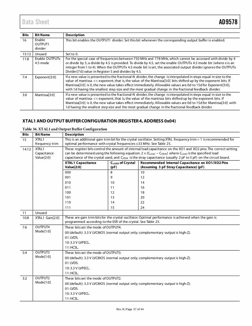
Data Sheet AD9578
Rev. B | Page 37 of 44
Bits Bit Name Description
16 Enable OUTPUT1 divider
This bit enables the OUTPUT1 divider. Set this bit whenever the corresponding output buffer is enabled.
15:12 Unused Set to 0. 11:8 Enable OUTPUTx
4.5 mode For the special case of frequencies between 750 MHz and 778 MHz, which cannot be accessed with divide by 4 or divide by 5, a divide by 4.5 is provided. To divide by 4.5, set the enable OUTPUTx 4.5 mode bit (where x is an integer from 1 to 4). When the OUTPUTx 4.5 mode bit is set, the associated output divider ignores the OUTPUTx Divider[7:0] value in Register 5 and divides by 4.5.
7:4 Exponent[3:0] If a new value is presented to the fractional-N divider, the change is interpolated in steps equal in size to the value of mantissa << exponent, that is, the value of the Mantissa[3:0] bits shifted up by the exponent bits. If Mantissa[3:0] is 0, the new value takes effect immediately. Allowable values are 0d to 15d for Exponent[3:0], with 1d having the smallest step size and the most gradual change in the fractional feedback divider.
3:0 Mantissa[3:0] If a new value is presented to the fractional-N divider, the change is interpolated in steps equal in size to the value of mantissa << exponent, that is, the value of the mantissa bits shifted up by the exponent bits. If Mantissa[3:0] is 0, the new value takes effect immediately. Allowable values are 0d to 15d for Mantissa[3:0] with 1d having the smallest step size and the most gradual change in the fractional feedback divider.
XTAL1 AND OUTPUT BUFFER CONFIGURATION (REGISTER 4, ADDRESS 0x04)
Table 36. XTAL1 and Output Buffer Configuration Bits Bit Name Description
15 XTAL1 frequency trim
This is an additional gain trim bit for the crystal oscillator. Setting XTAL frequency trim = 1 is recommended for optimal performance with crystal frequencies ≤33 MHz. See Table 25.
14:12 XTAL1 Capacitance Value[2:0]
These register bits control the amount of internal load capacitance on the XO1 and XO2 pins. The correct setting can be determined using the following equation: 2 × (CLOAD − CSTRAY) where CLOAD is the specified load capacitance of the crystal used, and CSTRAY is the stray capacitance (usually 2 pF to 5 pF) on the circuit board.
XTAL1 Capacitance Value[2:0]
CLOAD of Crystal (pF)
Recommended Internal Capacitance on XO1/XO2 Pins (Assuming 3 pF Stray Capacitance) (pF)
000 8 10 001 9 12
010 10 14 011 11 16 100 12 18 101 13 20 110 14 22
111 15 24
11 Unused 10:8 XTAL1 Gain[2:0] These are gain trim bits for the crystal oscillator. Optimal performance is achieved when the gain is
programmed according to the ESR of the crystal. See Table 25.
7:6 OUTPUT4 Mode[1:0]
These bits set the mode of OUTPUT4.
00 (default): 3.3 V LVCMOS (normal output only; complementary output is high-Z). 01: LVDS. 10: 3.3 V LVPECL. 11: HCSL.
5:4 OUTPUT3 Mode[1:0]
These bits set the mode of OUTPUT3.
00 (default): 3.3 V LVCMOS (normal output only; complementary output is high-Z). 01: LVDS.
10: 3.3 V LVPECL. 11: HCSL.
3:2 OUTPUT2 Mode[1:0]
These bits set the mode of OUTPUT2.
00 (default): 3.3 V LVCMOS (normal output only; complementary output is high-Z). 01: LVDS. 10: 3.3 V LVPECL. 11: HCSL.
AD9578 Data Sheet
Rev. B | Page 38 of 44
Bits Bit Name Description
1:0 OUTPUT1 Mode[1:0]
These bits set the mode of OUTPUT1.
00 (default): 3.3 V LVCMOS (normal output only; complementary output is high-Z). 01: LVDS.
10: 3.3 V LVPECL. 11: HCSL.
OUTPUT DRIVER CONFIGURATION (REGISTER 5, ADDRESS 0x05)
Table 37. Output Driver Configuration Bits Bit Name Description
31:24 OUTPUT4 Divider[7:0] The value of the OUTPUT4 divider. As an 8-bit decimal value, n, the VCO frequency is divided by n, where n = 4 to 255, and divided by 256 + n, where n = 0 to 3.
23:16 OUTPUT3 Divider[7:0] The value of the OUTPUT3 divider. As an 8-bit decimal value, n, the VCO frequency is divided by n, where n = 4 to 255, and divided by 256 + n, where n = 0 to 3.
15:8 OUTPUT2 Divider[7:0] The value of the OUTPUT2 divider. As an 8-bit decimal value, n, the VCO frequency is divided by n, where n = 4 to 255, and divided by 256 + n, where n = 0 to 3.
7:0 OUTPUT1 Divider[7:0] The value of the OUTPUT1 divider. As an 8-bit decimal value, n, the VCO frequency is divided by n, where n = 4 to 255, and divided by 256 + n, where n = 0 to 3.
PLL1 CONFIGURATION (REGISTER 6, ADDRESS 0x06)
Table 38. PLL1 Configuration Bits Bit Name Description
39:32 PLL1 Integer Feedback Divider[7:0]
PLL1 integer feedback divider. This is a fixed point value that contains the integer portion of the feedback divider. The smallest allowable value of the PLL1 feedback divider is 23.
31:10 PLL1 Fractional Feedback Divider[27:6]
PLL1 fractional feedback divider, Bits[27:6]. If PLL1 is in fractional mode, all 28 bits in the PLL1 fractional feedback divider are used. If PLL1 is in integer mode, the first three bits in this register can be used either for phase interpolation or for MASH modulation, according to the value of S[1:0]. In fractional mode, at full phase interpolation, the fractional portion of the PLL1 feedback divider is 28 bits, for a resolution of 1/(228), or 3.7 × 10⁻⁹, or approximately 4 ppb.
9:4 PLL1 Fractional Feedback Divider[5:0], PLL1 Modulus Value[5:0]
In fractional mode, this register contains Bits[5:0] of the PLL1 fractional feedback divider. In rational mode, this register contains Bits[5:0] of the PLL1 modulus value. This register is not used in integer mode; do not set the bits in this register to 0 in integer mode.
3 ENPFD This bit controls the power supplies to the charge pump and phase frequency detector. Keep this bit set to 1, the default setting. These subsystems are automatically disabled whenever the corresponding PLL is powered down via the PD1 pin.
2 VCO PU This bit controls the power supplies to the VCO. Keep this bit set to 1, the default setting. This subsystem is automatically disabled whenever the corresponding PLL is powered down via the PD1 pin.
1 Feedback divider PU This bit controls the power supplies to the feedback divider. Keep this bit set to 1, the default setting. This subsystem is automatically disabled whenever the corresponding PLL is powered down via the PD1 pin.
0 PLL1 lock IRQ This bit sets the function of the SDO/LOL pin. 0 (default): the SDO/LOL pin function is serial data output (SDO). 1: the SDO/LOL pin function is IRQ, which is used as a loss of lock (LOL) indicator.
Data Sheet AD9578
Rev. B | Page 39 of 44
PLL1 CONFIGURATION (REGISTER 7, ADDRESS 0x07)
Table 39. PLL1 Configuration Bits Bit Name Description
39:37 PLL1 Dither[2:0] Order of dither generation. When PLL1 Dither[2:0] is 0, there is no dithering. All nonzero values create dither of the value stored in PLL1 Dither[2:0]. Dither is a noise shaped random value that is added to the divider fractional value at each calculation of the modulation, which helps to disperse harmonic spurs resulting from short modulation sequences. The time average value of dither is always zero, so that the use of dither does not change the divider value. The use of dither is highly dependent upon the choice of value for Dither Scale[4:0]. For normal operation, always set PLL1 Dither[2:0] to zero when PLL1 MASH[2:0] is zero. The largest usable value of PLL1 Dither[2:0] is 5. Typically, the value of PLL1 Dither[2:0] is set equal to the value of PLL1 MASH[2:0].
36:32 Dither Scale[4:0]
Dither scale. The dither scale, in bits. The dither value is a signed value of one to five bits in length, depending on the value chosen for PLL1 Dither[2:0]. To be effective, this value must be scaled up until the amount of dither is equal to 1/2 LSB of the divider value. The proper dither scale value for the dither is therefore equal to the number of zeros following the last bit set to 1 in the feedback divider value. Because the dither is a signed value, Dither Scale[4:0] must always be larger than the PLL1 Dither[2:0] setting.
31:29 PLL1 MASH[2:0] The order of MASH modulation. When PLL1 MASH[2:0] = 0, there is no modulation. Any fractional value given to the feedback divider that is at a finer resolution than the phase interpolation, S[1:0], results in an inaccurate output frequency. For all nonzero values of PLL1 MASH[2:0], modulation is used unless the feedback divider does not require modulation to be represented exactly (for example, if the feedback divider is an integer number). Modulation means that the feedback divider alternates between floor(PLL1 Fractional Feedback Divider[27:0]) and ceiling(PLL1 Fractional Feedback Divider[27:0]) according to a pattern whose time averaged value is PLL1 Fractional Feedback Divider[27:0]. When PLL1 MASH[2:0] = 1, first-order modulation is used. First-order modulation typically has large noise spurs due to the short length of the modulation patterns. Noise decreases as a function of PLL1 MASH[2:0], although for values of PLL1 MASH[2:0] greater than 2, this effect may not be measurable. The largest usable value of PLL1 MASH[2:0] is 4.
28:24 PLL1 Frequency Select[4:0]
This 5-bit value sets the frequency range of the VCO. Smaller values correspond to higher frequency. The evaluation software sets the optimal value; therefore, the user does not normally need to change this register. Table 27 contains the frequency ranges for each register setting. Note that the PLL1 KVCO band bit in Register 0x0C must be set to 1 for Frequency Select[4:0] = 14 through 27 (decimal).
23 Power-on override
When set to 1, this bit, one for each PLL, disables the simultaneous synchronization pulses sent to PLL1 and PLL2 during the power-up cycle. Otherwise, both PLL outputs are synchronized at startup.
22:21 S[1:0] The order of phase interpolation. When S[1:0] = 0, a fractional divider is interpolated among eight phases; therefore, values down to 1/8 can be represented exactly, without modulation. When S[1:0] = 1, the value is interpolated among four phases. When S[1:0] = 2, the value is interpolated between two phases, and when S[1:0] = 3, there is no phase interpolation. For example, the feedback divider of 64.5 can be represented either by PLL1 MASH[2:0] = 0, S[1:0] = 2; or by PLL1 MASH[2:0] = 1, S[1:0] = 3. In both cases, the output frequency is the same. However, the phase noise characteristics of the two representations differ. The use of phase interpolation allows up to three bits greater precision in the feedback divider. A consequence of reducing the phase interpolation is the loss of bits at the end of PLL1 Fractional Feedback Divider[27:0]. For example, when S[1:0] = 2, the last bit of PLL1 Fractional Feedback Divider[27:0] is ignored.
20:16 CUR[4:0] Each PLL has a current trim for the charge pump, with the current given by the equation (3.125 × (1 + CUR)) μA, for a minimum current of 3.125 μA at CUR[4:0] = 0, and a maximum current of 100 μA at CUR[4:0] = 31.
15 PLL1 phase advance
This bit, one for each PLL, is an active control that shifts the output of the VCO forward one of eight phases (1/8 cycle). This phase shift happens regardless of the S[1:0] setting for the PLL. The phase advance is edge triggered; therefore, no further phase advancement occurs until this bit is set back to 0 and raised again. This feature can be used to precisely align the phases of the two PLLs.
14 Reset feedback divider
This bit resets the feedback divider. Set and clear this bit if the order of the MASH is changed or if the feedback divider in Register 6 is changed.
13 OUTPUT1_2 reset
This bit resets the OUTPUT1 and OUTPUT2 output driver. This bit is normally set to 0, although it can be set and cleared to reset the OUTPUT1 and OUTPUT2 output drivers.
12 Force reset This active signal forces a reset cycle that generates synchronization pulses for the outputs of each PLL. 11 PLL1 phase
retard This bit is similar to the advance bit but shifts the output of the VCO backward one of eight phases.
10 Rational mode This bit sets the rational mode, the use of which is described in detail in the PLLs section. In rational mode, the feedback divider fractional part is a ratio of integers, with the numerator encoded in PLL1 Fractional Feedback Divider[24:9] in Register 6and the denominator encoded in PLL1 Modulus Value[15:6] of this register.
AD9578 Data Sheet
Rev. B | Page 40 of 44
Bits Bit Name Description
9:0 PLL1 Modulus Value[15:6]
The first 10 bits of the 16-bit modulus value. When the 16-bit binary value is 0, the PLL1 Fractional Feedback Divider[27:0] value is interpreted as a 28-bit fixed point value. When PLL1 Modulus Value[15:0] is nonzero, and the rational mode bit is set, the feedback divider ratio is calculated by a complicated expression (see Table 26). In the simplest case, S[1:0] is set to 3 (no phase interpolation), and the feedback divider expression is PLL1 Fractional Feedback Divider[24:9] + (PLL1 Feedback Divider[24:9]/modulus), generating a feedback divider that is an exact ratio of integers. Note that having a numerator that is larger than the denominator is an invalid configuration. Also, note that the lower six bits of the modulus value are shared with the lowest six bits of PLL1 Feedback Divider[27:0], which are not otherwise used in rational mode.
PLL2 CONFIGURATION (REGISTER 8, ADDRESS 0x08)
Table 40. PLL2 Configuration Bits Bit Name Description
39:32 PLL2 Integer Feedback Divider[7:0]
PLL2 integer feedback divider. This is a fixed point value that contains the integer portion of the feedback divider. The smallest allowable value of the PLL1 feedback divider is 23.
31:10 PLL2 Fractional Feedback Divider[27:6]
PLL2 fractional feedback divider, Bits[27:6]. If PLL2 is in fractional mode, all 28 bits in the PLL2 fractional feedback divider are used. If PLL1 is in integer mode, the first three bits in this register can be used either for phase interpolation or for MASH modulation, according to the value of S[1:0]. In fractional mode at full phase interpolation, the fractional part of the PLL1 feedback divider is 28 bits, for a resolution of 1/(228), or 3.7 × 10⁻⁹, or approximately 4 ppb.
9:4 PLL2 Fractional Feedback Divider[5:0], PLL2 Modulus Value[5:0]
In fractional mode, this register contains Bits[5:0] of the PLL2 fractional feedback divider. In rational mode, this register contains Bits[5:0] of the PLL2 modulus value. This register is not used in integer mode; do not set the bits in this register to 0 in integer mode.
3 ENPFD This bit controls the power supplies to the charge pump and phase frequency detector. Keep this bit set to 1, the default setting. These subsystems are automatically disabled whenever the corresponding PLL is powered down via the PD1 pin.
2 VCO PU This bit controls the power supplies to the VCO. Keep this bit set to 1, the default setting. This subsystem is automatically disabled whenever the corresponding PLL is powered down via the PD1 pin.
1 Feedback divider PU
This bit controls the power supplies to the feedback divider. Keep this bit set to 1, the default setting. This subsystem is automatically disabled whenever the corresponding PLL is powered down via the PD1 pin.
0 PLL2 lock IRQ This bit sets the function of the SDO/LOL pin. (SDO changes to 0 (default): the SDO/LOL pin function is serial data output (SDO). IRQ) 1: the SDO/LOL pin function is IRQ, which is used as a loss of lock (LOL) indicator.
PLL2 CONFIGURATION (REGISTER 9, ADDRESS 0x09)
Table 41. PLL2 Configuration Bits Bit Name Description
39:37 PLL2 Dither[2:0] Order of dither generation. When PLL2 Dither[2:0] is 0, there is no dithering. All nonzero values create dither of the value stored in PLL2 Dither[2:0]. Dither is a noise shaped random value that is added to the divider fractional value at each calculation of the modulation, which helps to disperse harmonic spurs resulting from short modulation sequences. The time average value of dither is always zero, so that the use of dither does not change the divider value. The use of dither is highly dependent upon the choice of value for Dither Scale[4:0]. For normal operation, always set PLL2 Dither[2:0] to zero when PLL2 MASH[2:0] is zero. The largest usable value of PLL2 Dither[2:0] is 5. Typically, the value of PLL2 Dither[2:0] is set equal to the value of PLL2 MASH[2:0].
36:32 Dither Scale[4:0]
Dither scale. The dither scale, in bits. The dither value is a signed value of one to five bits in length, depending on the value chosen for PLL2 Dither[2:0]. To be effective, this value must be scaled up until the amount of dither is equal to 1/2 LSB of the divider value. The proper dither scale value for the dither is therefore equal to the number of zeros following the last bit set to 1 in the feedback divider value. Because the dither is a signed value, Dither Scale[4:0] must always be larger than the PLL2 Dither[2:0] setting.
Data Sheet AD9578
Rev. B | Page 41 of 44
Bits Bit Name Description
31:29 PLL2 MASH[2:0] The order of MASH modulation. When PLL2 MASH[2:0] = 0, there is no modulation. Any fractional value given to the feedback divider that is at a finer resolution than the phase interpolation, S[1:0], results in an inaccurate output frequency. For all nonzero values of PLL2 MASH[2:0], modulation is used unless the feedback divider does not require modulation to be represented exactly (for example, if the feedback divider is an integer number). Modulation means that the feedback divider alternates between floor(PLL2 Fractional Feedback Divider[27:0]) and ceiling(PLL2 Fractional Feedback Divider[27:0]) according to a pattern whose time averaged value is PLL2 Fractional Feedback Divider[27:0]. When PLL2 MASH[2:0] = 1, first-order modulation is used. First-order modulation typically has large noise spurs due to the short length of the modulation patterns. Noise decreases as a function of PLL2 MASH[2:0], although for values of PLL2 MASH[2:0] greater than 2, this effect may not be measurable. The largest usable value of PLL2 MASH[2:0] is 4.
28:24 PLL2 Frequency Select[4:0]
This 5-bit value sets the frequency range of the VCO. Smaller values correspond to higher frequency. The evaluation software sets the optimal value; therefore, the user does not normally need to change this register. Table 27 contains the frequency ranges for each register setting. Note that the PLL2 KVCO band bit in Register 0x0E must be set to 1 for PPL2 Frequency Select[4:0] = 14 through 27 (decimal).
23 Power-on override
When set to 1, this bit, one for each PLL, disables the simultaneous synchronization pulses sent to PLL1 and PLL2 during the power-up cycle. Otherwise, both PLL outputs are synchronized at startup.
22:21 S[1:0] The order of phase interpolation. When S[1:0] = 0, a fractional divider is interpolated among eight phases; therefore, values down to 1/8 can be represented exactly, without modulation. When S[1:0] = 1, the value is interpolated among four phases. When S[1:0] = 2, the value is interpolated between two phases, and when S[1:0] = 3, there is no phase interpolation. For example, the feedback divider of 64.5 can be represented either by PLL2 MASH[2:0] = 0, S[1:0] = 2; or by PLL2 MASH[2:0] = 1, S[1:0] = 3. In both cases, the output frequency is the same. However, the phase noise characteristics of the two representations differ. The use of phase interpolation allows up to three bits greater precision in the feedback divider. A consequence of reducing the phase interpolation is the loss of bits at the end of PLL2 Fractional Feedback Divider[27:0]. For example, when S[1:0] = 2, the last bit of PLL2 Fractional Feedback Divider[27:0] is ignored.
20:16 CUR[4:0] Each PLL has a current trim for the charge pump, with the current given by the equation (3.125 × (1 + CUR)) μA, for a minimum current of 3.125 μA at CUR[4:0] = 0, and a maximum current of 100 μA at CUR[4:0] = 31.
15 PLL2 phase advance
This bit, one for each PLL, is an active control that shifts the output of the VCO forward one of eight phases (1/8 cycle). This phase shift happens regardless of the S[1:0] setting for the PLL. The phase advance is edge triggered; therefore, no further phase advancement occurs until this bit is set back to 0 and raised again. This feature can be used to precisely align the phases of the two PLLs.
14 Reset feedback divider
This bit resets the feedback divider. Set and clear this bit if the order of the MASH is changed or if the feedback divider in Register 8 is changed.
13 OUTPUT3_4 reset
This bit resets the OUTPUT3 and OUTPUT4 output driver. This bit is normally set to 0, although it can be set and cleared to reset the OUTPUT3 and OUTPUT4 output drivers.
12 Force reset This active signal forces a reset cycle that generates synchronization pulses for the outputs of each PLL.
11 PLL2 phase retard
This bit is similar to the advance bit but shifts the output of the VCO backward one of eight phases.
10 Rational mode This bit sets the rational mode, the use of which is described in detail in the PLLs section. In rational mode, the feedback divider fractional part is a ratio of integers, with the numerator encoded in PLL2 Fractional Feedback Divider[24:9] in Register 8and the denominator encoded in PLL2 Modulus Value[15:6] of this register.
9:0 PLL2 Modulus Value[15:6]
The first 10 bits of the 16-bit modulus value. When the 16-bit binary value is 0, the PLL1 Fractional Feedback Divider[27:0] value is interpreted as a 28-bit fixed point value. When PLL1 Modulus Value[15:0] is nonzero, and the rational mode bit is set, the feedback divider ratio is calculated by a complicated expression (see Table 26). In the simplest case, S[1:0] is set to 3 (no phase interpolation), and the feedback divider expression is PLL1 Fractional Feedback Divider[24:9] + (PLL1 Feedback Divider[24:9]/modulus), generating a feedback divider that is an exact ratio of integers. Note that having a numerator that is larger than the denominator is an invalid configuration. Also, note that the lower six bits of the modulus value are shared with the lowest six bits of PLL1 Feedback Divider[27:0], which are not otherwise used in rational mode.
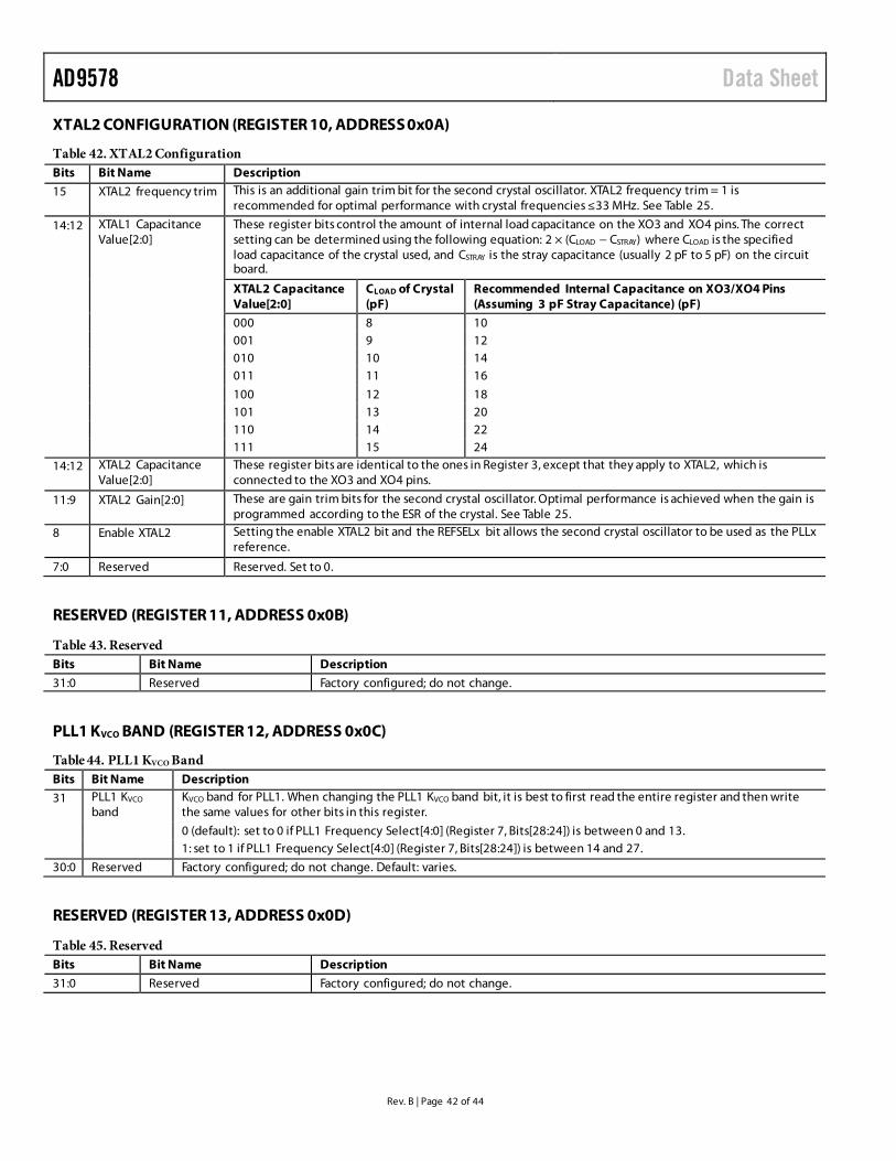
AD9578 Data Sheet
Rev. B | Page 42 of 44
XTAL2 CONFIGURATION (REGISTER 10, ADDRESS 0x0A)
Table 42. XTAL2 Configuration Bits Bit Name Description
15 XTAL2 frequency trim This is an additional gain trim bit for the second crystal oscillator. XTAL2 frequency trim = 1 is recommended for optimal performance with crystal frequencies ≤33 MHz. See Table 25.
14:12 XTAL1 Capacitance Value[2:0]
These register bits control the amount of internal load capacitance on the XO3 and XO4 pins. The correct setting can be determined using the following equation: 2 × (CLOAD − CSTRAY) where CLOAD is the specified load capacitance of the crystal used, and CSTRAY is the stray capacitance (usually 2 pF to 5 pF) on the circuit board.
XTAL2 Capacitance Value[2:0]
CLOAD of Crystal (pF)
Recommended Internal Capacitance on XO3/XO4 Pins (Assuming 3 pF Stray Capacitance) (pF)
000 8 10 001 9 12 010 10 14 011 11 16
100 12 18 101 13 20 110 14 22 111 15 24
14:12 XTAL2 Capacitance Value[2:0]
These register bits are identical to the ones in Register 3, except that they apply to XTAL2, which is connected to the XO3 and XO4 pins.
11:9 XTAL2 Gain[2:0] These are gain trim bits for the second crystal oscillator. Optimal performance is achieved when the gain is programmed according to the ESR of the crystal. See Table 25.
8 Enable XTAL2 Setting the enable XTAL2 bit and the REFSELx bit allows the second crystal oscillator to be used as the PLLx reference.
7:0 Reserved Reserved. Set to 0.
RESERVED (REGISTER 11, ADDRESS 0x0B)
Table 43. Reserved Bits Bit Name Description
31:0 Reserved Factory configured; do not change.
PLL1 KVCO BAND (REGISTER 12, ADDRESS 0x0C)
Table 44. PLL1 KVCO Band Bits Bit Name Description
31 PLL1 KVCO band
KVCO band for PLL1. When changing the PLL1 KVCO band bit, it is best to first read the entire register and then write the same values for other bits in this register.
0 (default): set to 0 if PLL1 Frequency Select[4:0] (Register 7, Bits[28:24]) is between 0 and 13. 1: set to 1 if PLL1 Frequency Select[4:0] (Register 7, Bits[28:24]) is between 14 and 27.
30:0 Reserved Factory configured; do not change. Default: varies.
RESERVED (REGISTER 13, ADDRESS 0x0D)
Table 45. Reserved Bits Bit Name Description
31:0 Reserved Factory configured; do not change.
Data Sheet AD9578
Rev. B | Page 43 of 44
PLL2 KVCO BAND (REGISTER 14, ADDRESS 0x0E)
Table 46. PLL2 KVCO Band Bits Bit Name Description
31 PLL2 KVCO band
KVCO band for PLL2. When changing the PLL2 KVCO band bit, it is best to first read the entire register and then write the same values for other bits in this register.
0 (default): set to 0 if PLL2 Frequency Select[4:0] (Register 9, Bits[28:24]) is between 0 and 13. 1: set to 1 if PLL2 Frequency Select[4:0] (Register 9, Bits[28:24]) is between 14 and 27.
30:0 Reserved Factory configured; do not change. Default: varies.
PLL LOCK DETECT (REGISTER 15, ADDRESS 0x0F)
Table 47. PLL Lock Detect (Read Only) Bits Bit Name Description
23 PLL2 lock detect PLL2 lock detect. 0: PLL2 is not locked, possibly indicating the absence of an input reference, or that the PLL is
misconfigured.
1: PLL2 is locked.
22 Reserved
21 PLL1 lock detect PLL1 lock detect. 0: PLL1 is not locked, possibly indicating the absence of an input reference, or that the PLL is
misconfigured.
1: PLL1 is locked.
20:19 Reserved Set to 00b.
18:17 Revision Subcode[1:0]
This 2-bit value gives the mask variant of the AD9578. Default: 01b
6 Reserved Default: 0x00
15:0 Unused Set to 0.
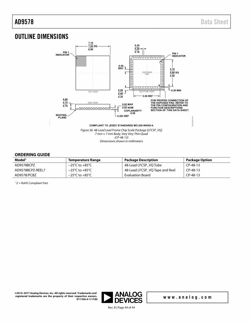
AD9578 Data Sheet
Rev. B | Page 44 of 44
OUTLINE DIMENSIONS
COMPLIANT TO JEDEC STANDARDS MO-220-WKKD-4.
FOR PROPER CONNECTION OFTHE EXPOSED PAD, REFER TOTHE PIN CONFIGURATION ANDFUNCTION DESCRIPTIONSSECTION OF THIS DATA SHEET.
1
0.50BSC
BOTTOM VIEWTOP VIEW
PIN 1INDICATOR
48
1324
3637
PIN 1INDICATOR
5.705.60 SQ5.50
0.500.400.30
SEATINGPLANE
0.800.750.70
0.05 MAX0.02 NOM
0.203 REF
COPLANARITY0.08
0.300.250.18
02-
29-2
016
-A
7.107.00 SQ6.90
0.20 MIN
5.50 REF
END VIEW
EXPOSEDPAD
PK
G-0
04
45
2
Figure 36. 48-Lead Lead Frame Chip Scale Package [LFCSP_VQ]
7 mm × 7 mm Body, Very Very Thin Quad (CP-48-13)
Dimensions shown in millimeters
ORDERING GUIDE Model1 Temperature Range Package Description Package Option AD9578BCPZ −25°C to +85°C 48-Lead LFCSP_VQ Tube CP-48-13 AD9578BCPZ-REEL7 −25°C to +85°C 48-Lead LFCSP_VQ Tape and Reel CP-48-13 AD9578/PCBZ −25°C to +85°C Evaluation Board CP-48-13 1 Z = RoHS Compliant Part.
©2014–2017 Analog Devices, Inc. All rights reserved. Trademarks and registered trademarks are the property of their respective owners. D11356-0-1/17(B)