AK1574 46.875-1682.5MHz Fractional-N PLL · The AK1574 is a fractional-N PLL synthesizer with a VCO...
66
[AK1574] 018001585-E-01 2018/05 - 1 - 1. General Description The AK1574 is a fractional-N PLL synthesizer with a VCO (Voltage Controlled Oscillator) that has frequency modulation function. It integrates an output divider for VCO signal that operates by 3365MHz frequency at maximum realizing wide range output frequency from 46.875MHz to 1682.5MHz. The AK1574 reduces the power consumption while realizing low normalized phase noise of -221dBc/Hz. It achieves 90mW(3V/Single output) operation when outputting -6dBm. It is capable of replacing VCOs, that use to consist of variable capacitance diode and etc., in various wireless applications especially suitable for hand portable wireless devices. The fast lock-up, that completes in only less than 1ms, suites for intermittent operation of PLL/VCO. It contributes to reducing the system power consumption. Two set of mode settings that include frequency setting and On/Off settings of RF output pins are available. Output Mode A: Frequency setting f Rx , RFOUT_A On, RFOUT_B Off (Single output) Output Mode B: Frequency setting f Tx , RFOUT_A Off, RFOUT_B On (Single output) By setting as above, the RFOUT_A pin can be used as receiving output and the RFOUT_B pin can be used as transmitting output. Output Mode A: Frequency f Rx , RFOUT_A On, RFOUT_B On (Differential Output) By setting as above, two lines of common-frequency can be output. It is able to use for diversity receivers. When both RFOUT_A and B are On, the signal is output as differential signal so that it is capable of being used as single differential output. Data input format for frequency modulation corresponds to both analog and digital data inputs. Digital I/F data format can be selected from I 2 S (Inter-IC Sound), Left-justified and SPI. The AK1574 has a frequency shift compensation function for TCXO that is used when shipping user’s product. Therefore, it is able to use TCXO instead of VCTCXO. 2. Features Output Frequency: 46.875MHz ~ 1682.5MHz Current Consumption: 30mA at 3V, 520.1MHz, -6dBm Output (Single Output) Supply Voltage/Temperature Range: 2.7 ~ 3.45V (IOVDD: 1.7V~ ) / -40 ~ +85ºC Frequency Modulation Supporting Analog Voice Data Input (FM/FSK) Various Digital I/F for Frequency Modulation Function (FM/FSK): I 2 S, Left-Justified, SPI Normalized Phase Noise: -221dBc/Hz (during fractional operation) In-band Phase Noise: -125dBc/Hz at 12.5kHz Offset, 420MHz Output, PFD Frequency=50.4MHz Frequency Resolution Under 10Hz by a 23-bit ΔΣ Modulator Driver amplifier with variable output power: -12 ~ +6dBm Output (Single Output) Two Output Ports for various application Faster Lock-up Time: <1ms Divided Reference Clock Output Function for Common System Clock REFCKIN Frequency: 10MHz ~ 60MHz Package: 36-pin QFN (5mm×5mm×0.75 mm, 0.4mm pitch) 3. Applications Professional Mobile Radio (DMR, NXDN, dPMR, TIA-603, STD-T98/102, etc.) FM/FSK transmitter AK1574 46.875-1682.5MHz Fractional-N PLL with integrated VCO and FM/FSK modulator
Transcript of AK1574 46.875-1682.5MHz Fractional-N PLL · The AK1574 is a fractional-N PLL synthesizer with a VCO...

[AK1574]
018001585-E-01 2018/05 - 1 -
1. General Description
The AK1574 is a fractional-N PLL synthesizer with a VCO (Voltage Controlled Oscillator) that has frequency modulation function. It integrates an output divider for VCO signal that operates by 3365MHz frequency at maximum realizing wide range output frequency from 46.875MHz to 1682.5MHz. The AK1574 reduces the power consumption while realizing low normalized phase noise of -221dBc/Hz. It achieves 90mW(3V/Single output) operation when outputting -6dBm. It is capable of replacing VCOs, that use to consist of variable capacitance diode and etc., in various wireless applications especially suitable for hand portable wireless devices. The fast lock-up, that completes in only less than 1ms, suites for intermittent operation of PLL/VCO. It contributes to reducing the system power consumption. Two set of mode settings that include frequency setting and On/Off settings of RF output pins are available.
Output Mode A: Frequency setting fRx, RFOUT_A On, RFOUT_B Off (Single output) Output Mode B: Frequency setting fTx, RFOUT_A Off, RFOUT_B On (Single output)
By setting as above, the RFOUT_A pin can be used as receiving output and the RFOUT_B pin can be used as transmitting output.
Output Mode A: Frequency fRx, RFOUT_A On, RFOUT_B On (Differential Output) By setting as above, two lines of common-frequency can be output. It is able to use for diversity receivers. When both RFOUT_A and B are On, the signal is output as differential signal so that it is capable of being used as single differential output. Data input format for frequency modulation corresponds to both analog and digital data inputs. Digital I/F data format can be selected from I
2S (Inter-IC Sound), Left-justified and SPI. The AK1574 has a
frequency shift compensation function for TCXO that is used when shipping user’s product. Therefore, it is able to use TCXO instead of VCTCXO.
2. Features
Output Frequency: 46.875MHz ~ 1682.5MHz Current Consumption: 30mA at 3V, 520.1MHz, -6dBm Output (Single Output) Supply Voltage/Temperature Range: 2.7 ~ 3.45V (IOVDD: 1.7V~ ) / -40 ~ +85ºC Frequency Modulation Supporting Analog Voice Data Input (FM/FSK) Various Digital I/F for Frequency Modulation Function (FM/FSK): I
2S, Left-Justified, SPI
Normalized Phase Noise: -221dBc/Hz (during fractional operation) In-band Phase Noise: -125dBc/Hz at 12.5kHz Offset, 420MHz Output, PFD
Frequency=50.4MHz Frequency Resolution Under 10Hz by a 23-bit ΔΣ Modulator Driver amplifier with variable output power: -12 ~ +6dBm Output (Single Output) Two Output Ports for various application Faster Lock-up Time: <1ms Divided Reference Clock Output Function for Common System Clock REFCKIN Frequency: 10MHz ~ 60MHz Package: 36-pin QFN (5mm×5mm×0.75 mm, 0.4mm pitch)
3. Applications
Professional Mobile Radio (DMR, NXDN, dPMR, TIA-603, STD-T98/102, etc.) FM/FSK transmitter
AK1574 46.875-1682.5MHz Fractional-N PLL
with integrated VCO and FM/FSK modulator

[AK1574]
018001585-E-01 2018/05 - 2 -
4. Table of Contents
1. General Description ............................................................................................................................ 1 2. Features .............................................................................................................................................. 1 3. Applications ......................................................................................................................................... 1 4. Table of Contents ................................................................................................................................ 2 5. Block Diagram and Functions ............................................................................................................. 4
5.1. Block Diagram .............................................................................................................................. 4 6. Pin Configurations and Functions ....................................................................................................... 5
6.1. Pin Layout .................................................................................................................................... 5 6.2. Pin Functions ............................................................................................................................... 5 6.3. Handling of Unused Pin ............................................................................................................... 7
7. Absolute Maximum Ratings ................................................................................................................ 8 8. Recommended Operating Conditions ................................................................................................. 9 9. Digital Characteristics ......................................................................................................................... 9
9.1. DC Characteristics ....................................................................................................................... 9 9.2. System Reset ............................................................................................................................. 10 9.3. Serial Interface Timing for Register Accessing ......................................................................... 11 9.4. Serial Interface Timing of Modulation Signal Input .................................................................... 12
10. Analog Characteristics .................................................................................................................. 14 11. Typical Performance ..................................................................................................................... 16
11.1. Output Power ......................................................................................................................... 16 11.2. Current Consumption ............................................................................................................. 17 11.3. Tuning Sensitivity(KVCO) ......................................................................................................... 18 11.4. VCO Phase Noise .................................................................................................................. 19 11.5. Closed Loop Phase Noise ..................................................................................................... 21 11.6. Lock-up Time.......................................................................................................................... 22 11.7. REFCK BUFFER .................................................................................................................... 22 11.8. REFCK DIVIDER ................................................................................................................... 23 11.9. ADC ........................................................................................................................................ 23 11.10. Modulation Characteristics ..................................................................................................... 25 11.11. Wide-band Spurious(WBS) .................................................................................................... 26 11.12. Integer Boundary Spurious(IBS) ............................................................................................ 27
12. Power-Up Sequence ..................................................................................................................... 30 12.1. Power-up Sequence ............................................................................................................... 30
13. Functional Description ................................................................................................................... 33 13.1. MULTIPLIER / R COUNTER ................................................................................................. 33 13.2. Frequency Stetting ................................................................................................................. 34 13.3. Re-lock up event .................................................................................................................... 37 13.4. Fast Lock-Up Mode ................................................................................................................ 37 13.5. VCO ........................................................................................................................................ 38 13.6. LOOP FILTER ........................................................................................................................ 39 13.7. LOCK DETECTOR ................................................................................................................. 40 13.8. Single/Differential Output ....................................................................................................... 42 13.9. ADC ........................................................................................................................................ 43 13.10. Modulation .............................................................................................................................. 45 13.11. REFDIVOUT Reference Frequency Divided Output ............................................................. 46
14. Register Map ................................................................................................................................. 47 14.1. Register Map .......................................................................................................................... 47 14.2. Special Register Access ........................................................................................................ 50 14.3. Register Definitions ................................................................................................................ 51
15. External Circuits ............................................................................................................................ 61 15.1. Reference Evaluation Board .................................................................................................. 61 15.2. PCB Design ............................................................................................................................ 63
16. Package ......................................................................................................................................... 64 16.1. Outline Dimensions ................................................................................................................ 64 16.2. Marking ................................................................................................................................... 64
17. Ordering Guide .............................................................................................................................. 65
[AK1574]
018001585-E-01 2018/05 - 3 -
18. Revision History ............................................................................................................................. 65
[AK1574]
018001585-E-01 2018/05 - 4 -
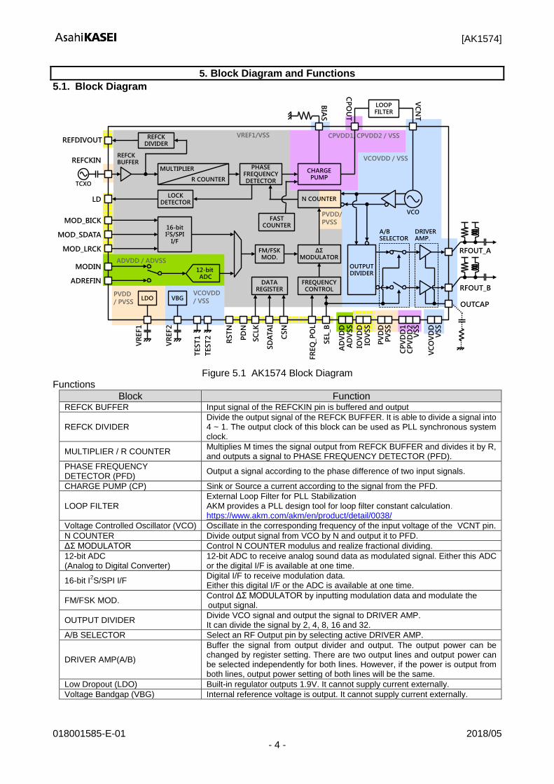
5. Block Diagram and Functions
5.1. Block Diagram
Figure 5.1 AK1574 Block Diagram
Functions
Block Function REFCK BUFFER Input signal of the REFCKIN pin is buffered and output
REFCK DIVIDER Divide the output signal of the REFCK BUFFER. It is able to divide a signal into 4 ~ 1. The output clock of this block can be used as PLL synchronous system clock.
MULTIPLIER / R COUNTER Multiplies M times the signal output from REFCK BUFFER and divides it by R, and outputs a signal to PHASE FREQUENCY DETECTOR (PFD).
PHASE FREQUENCY DETECTOR (PFD)
Output a signal according to the phase difference of two input signals.
CHARGE PUMP (CP) Sink or Source a current according to the signal from the PFD.
LOOP FILTER External Loop Filter for PLL Stabilization AKM provides a PLL design tool for loop filter constant calculation. https://www.akm.com/akm/en/product/detail/0038/
Voltage Controlled Oscillator (VCO) Oscillate in the corresponding frequency of the input voltage of the VCNT pin.
N COUNTER Divide output signal from VCO by N and output it to PFD.
ΔΣ MODULATOR Control N COUNTER modulus and realize fractional dividing.
12-bit ADC (Analog to Digital Converter)
12-bit ADC to receive analog sound data as modulated signal. Either this ADC or the digital I/F is available at one time.
16-bit I2S/SPI I/F
Digital I/F to receive modulation data. Either this digital I/F or the ADC is available at one time.
FM/FSK MOD. Control ΔΣ MODULATOR by inputting modulation data and modulate the output signal.
OUTPUT DIVIDER Divide VCO signal and output the signal to DRIVER AMP. It can divide the signal by 2, 4, 8, 16 and 32.
A/B SELECTOR Select an RF Output pin by selecting active DRIVER AMP.
DRIVER AMP(A/B)
Buffer the signal from output divider and output. The output power can be changed by register setting. There are two output lines and output power can be selected independently for both lines. However, if the power is output from both lines, output power setting of both lines will be the same.
Low Dropout (LDO) Built-in regulator outputs 1.9V. It cannot supply current externally.
Voltage Bandgap (VBG) Internal reference voltage is output. It cannot supply current externally.
VREF1/VSS CPVDD1, CPVDD2 / VSS
VCOVDD / VSS
ADVDD / ADVSS
VCOVDD
/ VSSPVDD
/ PVSS
PVDD/
PVSS
REFCKINREFCKBUFFER
LDLOCK
DETECTOR
PHASEFREQUENCYDETECTOR
MOD_BICK
MOD_SDATA
MOD_LRCK
16-bitI2S/SPI
I/F
MODIN
ADREFIN
12-bitADC
DATAREGISTER
SC
LK
SD
ATA
I
CSN
FREQUENCYCONTROL
FR
EQ
_PO
L
SEL_B
FM/FSKMOD.
ΔΣMODULATOR
N COUNTER
CHARGEPUMP
FASTCOUNTER
BIA
S
CP
OU
T
LOOPFILTER
VC
NT
PD
N
OUTPUTDIVIDER
DRIVERAMP.
VCO
LDO
VR
EF1
VBG
TEST
1
RFOUT_B
RFOUT_A
IOV
DD
PV
DD
PV
SS
CP
VD
D1
CP
VD
D2
VSS
OUTCAP
VC
OV
DD
VSS
IOV
SS
VR
EF2
TEST
2
TCXO
REFCKDIVIDER
REFDIVOUT
AD
VD
DA
DV
SS
RST
NA/BSELECTOR
MULTIPLIER
R COUNTER
[AK1574]
018001585-E-01 2018/05 - 5 -
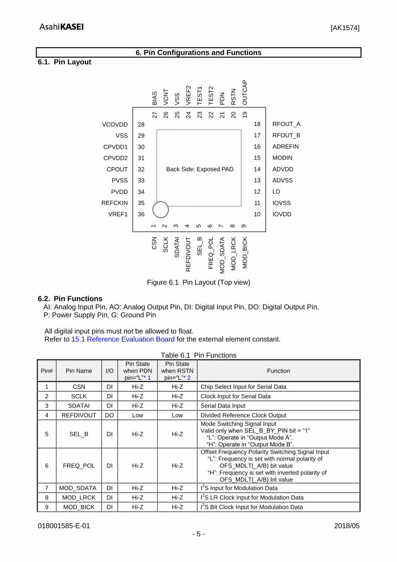
6. Pin Configurations and Functions
6.1. Pin Layout
RFOUT_A
RFOUT_B
ADREFIN
MODIN
ADVDD
ADVSS
LD
IOVSS
IOVDD
Back Side: Exposed PAD
1
2
3
4
5
6
7
8
9
18
17
16
15
14
13
12
11
10
CS
N
SC
LK
SD
ATA
I
RE
FD
IVO
UT
SE
L_
B
FR
EQ
_P
OL
MO
D_L
RC
K
MO
D_B
ICK
MO
D_S
DA
TA
27
25
24
23
22
21
20
19
26
BIA
S
VC
NT
VS
S
VR
EF
2
TE
ST
1
TE
ST
2
PD
N
RS
TN
OU
TC
AP
VCOVDD
VSS
CPVDD1
CPVDD2
CPOUT
PVSS
PVDD
REFCKIN
VREF1
30
28
29
31
32
33
34
35
36
Figure 6.1 Pin Layout (Top view)
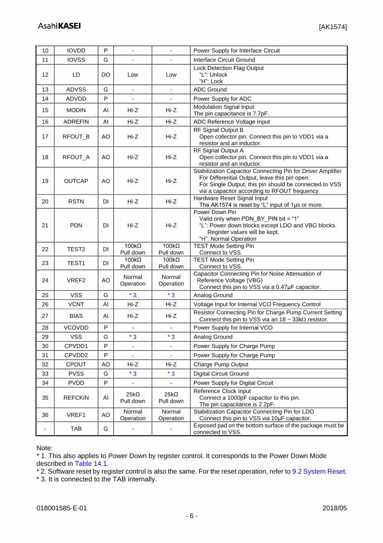
6.2. Pin Functions AI: Analog Input Pin, AO: Analog Output Pin, DI: Digital Input Pin, DO: Digital Output Pin, P: Power Supply Pin, G: Ground Pin All digital input pins must not be allowed to float. Refer to 15.1 Reference Evaluation Board for the external element constant.
Table 6.1 Pin Functions
Pin# Pin Name I/O Pin State
when PDN pin=“L”* 1
Pin State when RSTN pin=“L”* 2
Function
1 CSN DI Hi-Z Hi-Z Chip Select Input for Serial Data
2 SCLK DI Hi-Z Hi-Z Clock Input for Serial Data
3 SDATAI DI Hi-Z Hi-Z Serial Data Input
4 REFDIVOUT DO Low Low Divided Reference Clock Output
5 SEL_B DI Hi-Z Hi-Z
Mode Switching Signal Input Valid only when SEL_B_BY_PIN bit = “1”
“L”: Operate in “Output Mode A”. “H”: Operate in “Output Mode B”.
6 FREQ_POL DI Hi-Z Hi-Z
Offset Frequency Polarity Switching Signal Input “L”: Frequency is set with normal polarity of
OFS_MDLT(_A/B) bit value “H”: Frequency is set with inverted polarity of
OFS_MDLT(_A/B) bit value
7 MOD_SDATA DI Hi-Z Hi-Z I2S Input for Modulation Data
8 MOD_LRCK DI Hi-Z Hi-Z I2S LR Clock Input for Modulation Data
9 MOD_BICK DI Hi-Z Hi-Z I2S Bit Clock Input for Modulation Data
[AK1574]
018001585-E-01 2018/05 - 6 -
10 IOVDD P - - Power Supply for Interface Circuit
11 IOVSS G - - Interface Circuit Ground
12 LD DO Low Low Lock Detection Flag Output
“L”: Unlock “H”: Lock
13 ADVSS G - - ADC Ground
14 ADVDD P - - Power Supply for ADC
15 MODIN AI Hi-Z Hi-Z Modulation Signal Input The pin capacitance is 7.7pF.
16 ADREFIN AI Hi-Z Hi-Z ADC Reference Voltage Input
17 RFOUT_B AO Hi-Z Hi-Z RF Signal Output B
Open collector pin. Connect this pin to VDD1 via a resistor and an inductor.
18 RFOUT_A AO Hi-Z Hi-Z RF Signal Output A
Open collector pin. Connect this pin to VDD1 via a resistor and an inductor.
19 OUTCAP AO Hi-Z Hi-Z
Stabilization Capacitor Connecting Pin for Driver Amplifier For Differential Output, leave this pin open. For Single Output, this pin should be connected to VSS via a capacitor according to RFOUT frequency.
20 RSTN DI Hi-Z Hi-Z Hardware Reset Signal Input
The AK1574 is reset by “L” input of 1μs or more.
21 PDN DI Hi-Z Hi-Z
Power Down Pin Valid only when PDN_BY_PIN bit = “1” “L”: Power down blocks except LDO and VBG blocks.
Register values will be kept. “H”: Normal Operation
22 TEST2 DI 100kΩ
Pull down 100kΩ
Pull down TEST Mode Setting Pin
Connect to VSS.
23 TEST1 DI 100kΩ
Pull down 100kΩ
Pull down TEST Mode Setting Pin
Connect to VSS.
24 VREF2 AO Normal
Operation Normal
Operation
Capacitor Connecting Pin for Noise Attenuation of Reference Voltage (VBG) Connect this pin to VSS via a 0.47μF capacitor.
25 VSS G * 3 * 3 Analog Ground
26 VCNT AI Hi-Z Hi-Z Voltage Input for Internal VCO Frequency Control
27 BIAS AI Hi-Z Hi-Z Resistor Connecting Pin for Charge Pump Current Setting
Connect this pin to VSS via an 18 ~ 33k resistor.
28 VCOVDD P - - Power Supply for Internal VCO
29 VSS G * 3 * 3 Analog Ground
30 CPVDD1 P - - Power Supply for Charge Pump
31 CPVDD2 P - - Power Supply for Charge Pump
32 CPOUT AO Hi-Z Hi-Z Charge Pump Output
33 PVSS G * 3 * 3 Digital Circuit Ground
34 PVDD P - - Power Supply for Digital Circuit
35 REFCKIN AI 25kΩ
Pull down 25kΩ
Pull down
Reference Clock Input Connect a 1000pF capacitor to this pin. The pin capacitance is 2.2pF.
36 VREF1 AO Normal
Operation Normal
Operation Stabilization Capacitor Connecting Pin for LDO
Connect this pin to VSS via 10μF capacitor.
- TAB G - - Exposed pad on the bottom surface of the package must be connected to VSS.
Note: * 1. This also applies to Power Down by register control. It corresponds to the Power Down Mode described in Table 14.1. * 2. Software reset by register control is also the same. For the reset operation, refer to 9.2 System Reset. * 3. It is connected to the TAB internally.
[AK1574]
018001585-E-01 2018/05 - 7 -
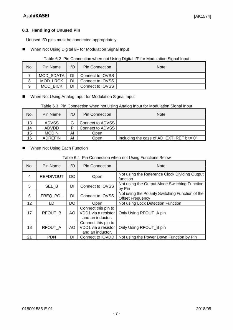
6.3. Handling of Unused Pin
Unused I/O pins must be connected appropriately. When Not Using Digital I/F for Modulation Signal Input
Table 6.2 Pin Connection when not Using Digital I/F for Modulation Signal Input
No. Pin Name I/O Pin Connection Note
7 MOD_SDATA DI Connect to IOVSS
8 MOD_LRCK DI Connect to IOVSS
9 MOD_BICK DI Connect to IOVSS
When Not Using Analog Input for Modulation Signal Input
Table 6.3 Pin Connection when not Using Analog Input for Modulation Signal Input
No. Pin Name I/O Pin Connection Note
13 ADVSS G Connect to ADVSS
14 ADVDD P Connect to ADVSS
15 MODIN AI Open
16 ADREFIN AI Open Including the case of AD_EXT_REF bit="0"
When Not Using Each Function
Table 6.4 Pin Connection when not Using Functions Below
No. Pin Name I/O Pin Connection Note
4 REFDIVOUT DO Open Not using the Reference Clock Dividing Output function
5 SEL_B DI Connect to IOVSS Not using the Output Mode Switching Function by Pin
6 FREQ_POL DI Connect to IOVSS Not using the Polarity Switching Function of the Offset Frequency
12 LD DO Open Not using Lock Detection Function
17 RFOUT_B AO Connect this pin to VDD1 via a resistor
and an inductor. Only Using RFOUT_A pin
18 RFOUT_A AO Connect this pin to VDD1 via a resistor
and an inductor. Only Using RFOUT_B pin
21 PDN DI Connect to IOVDD Not using the Power Down Function by Pin

[AK1574]
018001585-E-01 2018/05 - 8 -
7. Absolute Maximum Ratings
Table 7.1 Absolute Maximum Ratings
(PVSS=ADVSS=IOVSS=VSS=0V; * 4)
Parameter Symbol Min. Max. Unit
Power Supply
VCOVDD pin
CPVDD1 pin
CPVDD2 pin
PVDD pin
VDD1 -0.3 3.8 V
ADVDD pin ADVDD -0.3 4.3 V
IOVDD pin IOVDD -0.3 4.3 V
Analog Input Voltage
REFCKIN pin VAIN1 -0.3 VDD1+0.3
(≤ 3.8)
V MODIN pin
ADREFIN pin VAIN2 -0.3
ADVDD+0.3
(≤ 4.3)
VCNT pin VAIN3 -0.3 2.5
Digital Input Voltage
TEST1 pin
TEST2 pin VDIN1 -0.3
VDD1+0.3
(≤3.8) V
RSTN pin
PDN pin
SCLK pin
SDATAI pin
CSN pin
MOD_BICK pin
MOD_SDATA pin
MOD_LRCK pin
SEL_B pin
FREQ_POL pin
VDIN2 -0.3 IOVDD+0.3
(≤4.3) V
Input Current
(Input pins except power supply) IIN -10 +10 mA
Storage Temperature TSTG -55 125 ºC
Note: * 4. All voltages are with respect to ground. PVSS, ADVSS, IOVSS and VSSs must be connected to the
same ground. WARNING: Operation at or beyond these limits may result in permanent damage to the device. Normal
operation is not guaranteed at these extremes.

[AK1574]
018001585-E-01 2018/05 - 9 -
8. Recommended Operating Conditions
Table 8.1 Recommended Operating Conditions
(PVSS=ADVSS=IOVSS=VSS=0V; * 5)
Parameter symbol Min. Typ. Max. Unit
Ambient Temperature Ta -40 +85 ºC
Power Supply
VDD1 2.7 3.0 3.45 V
ADVDD 2.7 3.0 3.6 V
IOVDD 1.7 3.6 V
Note: * 5. All voltages are with respect to ground. PVSS, ADVSS, IOVSS and VSSs must be connected to the
same ground. WARNING: AKM assumes no responsibility for the usage beyond the conditions in the datasheet.
9. Digital Characteristics
9.1. DC Characteristics
Table 9.1 Digital DC Characteristics
Parameter Symbol Min. Typ. Max. Unit
High Input Voltage * 6 VIH 0.8×IOVDD V
Low Input Voltage * 6 VIL 0.2×IOVDD V
High Input Current 1 VIH=IOVDD=3.6V, * 6 IIH1 -1 +1 µA
High Input Current 2 VIH=IOVDD=3.6V, * 7 IIH2 +18 +36 +72 µA
Low Input Current VIL=0V, IOVDD=3.6V, * 6 IIL -1 +1 µA
High Output Voltage IOH=+500μA, * 8 VOH 0.85×IOVDD V
Low Output Voltage IOL=-500μA, * 8 VOL 0.15×IOVDD V
Regarding the input current, the direction in which the current flows into the IC is defined as + and the direction in which the current flows out from the IC is defined as -. Notes: * 6. RSTN, PDN, SCLK, SDATAI, CSN, MOD_BICK, MOD_SDATA, MOD_LRCK, SEL_B and
FREQ_POL pins * 7. TEST1 and TEST2 pins * 8. LD and REFDIVOUT pins
[AK1574]
018001585-E-01 2018/05 - 10 -
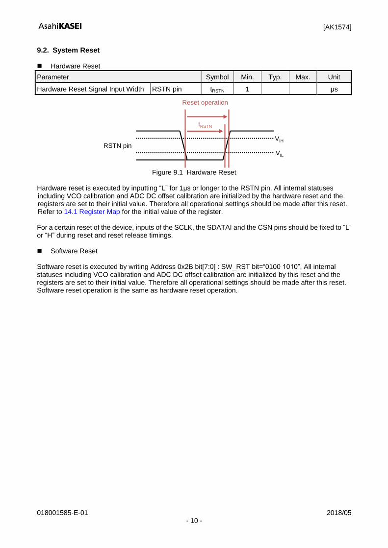
9.2. System Reset Hardware Reset
Parameter Symbol Min. Typ. Max. Unit
Hardware Reset Signal Input Width RSTN pin tRSTN 1 μs
Figure 9.1 Hardware Reset
Hardware reset is executed by inputting “L” for 1μs or longer to the RSTN pin. All internal statuses including VCO calibration and ADC DC offset calibration are initialized by the hardware reset and the registers are set to their initial value. Therefore all operational settings should be made after this reset. Refer to 14.1 Register Map for the initial value of the register. For a certain reset of the device, inputs of the SCLK, the SDATAI and the CSN pins should be fixed to “L” or “H” during reset and reset release timings. Software Reset Software reset is executed by writing Address 0x2B bit[7:0] : SW_RST bit=“0100 1010”. All internal statuses including VCO calibration and ADC DC offset calibration are initialized by this reset and the registers are set to their initial value. Therefore all operational settings should be made after this reset. Software reset operation is the same as hardware reset operation.
VIL
VIH
tRSTN
Reset operation
RSTN pin
[AK1574]
018001585-E-01 2018/05 - 11 -
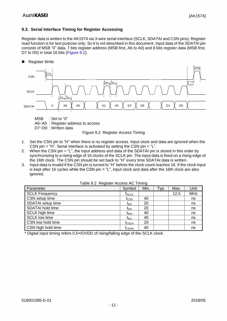
9.3. Serial Interface Timing for Register Accessing Register data is written to the AK1574 via 3-wire serial interface (SCLK, SDATAI and CSN pins). Register read function is for test purpose only. So it is not described in this document. Input data of the SDATAI pin consists of MSB “0” data, 7 bits register address (MSB first, A6 to A0) and 8 bits register data (MSB first, D7 to D0) in total 16 bits (Figure 9.2). Register Write
MSB : Set to “0” A6~A0 : Register address to access D7~D0 : Written data
Figure 9.2 Register Access Timing 1. Set the CSN pin to “H” when there is no register access. Input clock and data are ignored when the
CSN pin = “H”. Serial interface is activated by setting the CSN pin = “L”. 2. When the CSN pin = “L”, the input address and data of the SDATAI pin is stored in this order by
synchronizing to a rising edge of 16 clocks of the SCLK pin. The input data is fixed on a rising edge of the 16th clock. The CSN pin should be set back to “H” every time SDATAI data is written.
3. Input data is invalid if the CSN pin is turned to “H” before the clock count reaches 16. If the clock input is kept after 16 cycles while the CSN pin = “L”, input clock and data after the 16th clock are also ignored.
Table 9.2 Register Access AC Timing
Parameter Symbol Min. Typ. Max. Unit
SCLK Frequency fSCLK 12.5 MHz
CSN setup time tCSS 40 ns
SDATAI setup time tDS 20 ns
SDATAI hold time tDH 20 ns
SCLK high time tWH 40 ns
SCLK low time tWL 40 ns
CSN low hold time tCSLH 20 ns
CSN high hold time tCSHH 40 ns
* Digital input timing refers 0.5×IOVDD of rising/falling edge of the SCLK clock.
CSN
SCLK
SDATAI 0 A6 A5 A1 A0 D7 D6 D1 D0
tDS
tCSS
tDH
tWH tWL tCSLH
tCSHH

[AK1574]
018001585-E-01 2018/05 - 12 -
9.4. Serial Interface Timing of Modulation Signal Input Modulation signal is input to the AK1574 via 3-wire serial interface (MOD_BICK, MOD_SDATA and MOD_LRCK pins). Input data format can be selected from Left-Justified, I
2S or SPI by setting MOD_SPI
bit and MOD_LEFT bit. MOD_LRCK frequency equals to the sampling range of a modulation signal. Refer to 13.10 Modulation for the selection of the writing format of the digital modulation signal. Input data of the MOD_SDATA pin consists of 16 bits (2's complement, MSB first, D15-D0) and it is written in synchronization of a rising edge of a bit clock from the MOD_BICK pin. After the MOD_LRCK pin status is changed to “L” from “H”, MSB data is written on the first rising edge of the bit clock if the data is in Left-Justified and SPI formats, and MSB data is written on the second rising edge of the bit clock if the data is in I
2S format as shown in Figure 9.3 ~ Figure 9.5. Input data is fixed on the 15th rising edge of
the bit clock after writing MSB data (when LSB is written). Input data is invalid if the “L” period of the MOD_LRCK pin is shorter than 16 cycles of the bit clock. When “L” period of the MOD_LRCK is longer than 16 cycles, input data is valid for first 16 bits including MSB. Necessary “H” period of MOD_LRCK in Left-Justified or I
2S format is only 1 cycle of the bit clock.
I
2S
After a falling edge of LR clock, MSB is written in second bit. (delays one bit as Left-justified)
Figure 9.3 I
2S Format
Left-Justified MSB is written as soon as LR clock falls.
Figure 9.4 Left-Justified Format
SPI MOD_BICK is stopped when Left-Justified MOD_LRCK = “H”. Even if MOD_BICK is input when
MOD_LRCK = "H", operation is not affected.
Figure 9.5 SPI Format
MOD_LRCK
MOD_BICK
MOD_SDATA X D15 D14 D2 D1 D0 X X D15 D14
tDSM tDHM
tWHM tWLM
tCSSM
MOD_LRCK
MOD_BICK
MOD_SDATA D15 D14 D13 D1 D0 X X D15 D14 D13
tDSM tDHM
tWHM tWLM
tCSSM
MOD_LRCKas CSN
MOD_BCKas SCLK
MOD_SDATAas SDATAI D15 D14 D13 D8 D7 D6 D5 D1 D0
tDSM
tCSSM
tDHM
tWHM tWLM tCSLHM
tCSHHM
[AK1574]
018001585-E-01 2018/05 - 13 -
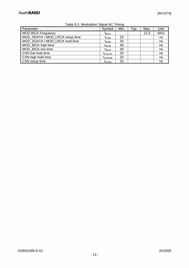
Table 9.3 Modulation Signal AC Timing
Parameter Symbol Min. Typ. Max. Unit
MOD BICK Frequency fBICK 12.5 MHz
MOD_SDATA / MOD_LRCK setup time tDSM 20 ns
MOD_SDATA / MOD_LRCK hold time tDHM 20 ns
MOD_BICK high time tWHM 40 ns
MOD_BICK low time tWLM 40 ns
CSN low hold time tCSLHM 20 ns
CSN high hold time tCSHHM 20 ns
CSN setup time tCSSM 20 ns

[AK1574]
018001585-E-01 2018/05 - 14 -
10. Analog Characteristics
(Ta= -40 ~ +85ºC; VDD1= 2.7 ~ 3.45V, ADVDD=2.7 ~ 3.6V, IOVDD=1.7 ~ 3.6V; Connect the BIAS pin to
VSS via a 27k resistor; Test circuit is shown in 15.1 Reference Evaluation Board, unless otherwise specified)
Table 10.1 Analog Characteristics
Parameter Min. Typ. Max. Unit Description
REFCK BUFFER
Input Sensitivity 0.2 VDD1 Vp-p REFCKIN pin
Operating Frequency Range 10 60 MHz fREF
MULTIPLIER
Operating Frequency Range 350 505 MHz fMULTI: fREF * MULT
PFD
Operating Frequency Range * 9
10 60 MHz fPFD: PFD Frequency
CHARGE PUMP
CP External Resistor for Current Adjustment
18 27 33 kΩ Connected to BIAS pin
CP Current
1200 μA 4 levels by ICP_FAST bit ICP_NORM bit
900 μA
600 μA
300 μA
VCO
Operating Frequency Range 1500 2100 MHz LVCO
2100 3365 MHz HVCO
VCO Tuning Sensitivity 0.02 × fVCO MHz/V fVCO: Oscillation Frequency
Acquisition Frequency Range * 10
-0.001 × fVCO
0.001 ×
fVCO MHz
RF Output Characteristics Differential Output
(mode A) / (mode B) OUTA_REG_A bit=”1” / OUTA_REG_B bit=”1” OUTB_REG_A bit=”1” / OUTB_REG_B bit=”1”
Phase Noise at 420MHz * 11
6.25kHz Offset -124
dBc/Hz
12.5kHz Offset -125
25kHz Offset -125
50kHz Offset -125
100kHz Offset -124
225kHz Offset -124
1MHz Offset -139
Normalized Phase Noise * 11
-221 dBc/Hz
FoM=
-20×log10(fOUT/fPFD)
-10×log10(fPFD) + CN
Output Power at 520.1MHz
3 dBm OUTLV(_A/B) bit =”111”
-3 dBm =”011”
-9 dBm =”001”
-15 dBm =”000”
[AK1574]
018001585-E-01 2018/05 - 15 -
Output Frequency Range * 12
1050 1682.5 MHz HVCO, DIV2
750 1050 MHz LVCO, DIV2
525 841.25 MHz HVCO, DIV4
375 525 MHz LVCO, DIV4
262.5 420.625 MHz HVCO, DIV8
187.5 262.5 MHz LVCO, DIV8
131.25 210.312 MHz HVCO, DIV16
93.75 131.25 MHz LVCO, DIV16
65.625 105.156 MHz HVCO, DIV32
46.875 65.625 MHz LVCO, DIV32
ADC
Resolution 12 bit
Signal to Noise and Distortion ratio
(SINAD) 55 63 dB
Input signal : (ADVDD – 0.1V) Vp-p sine wave fMODIN=1kHz
Sampling Rate 100 400 kHz ADVDD ≥ 2.7V
400 800 kHz ADVDD ≥ 3.0V
Zero Scale Input Voltage 0 V
Full Scale Input Voltage ADVDD V
REFCK DIVIDER
Maximum Output Frequency 20 MHz CLOAD=20pF
IOVDD ≥ 1.7V, REFDIVOUT_DS bit=”1”
Maximum Output Frequency 20 MHz CLOAD=20pF IOVDD ≥ 2.7V, REFDIVOUT_DS bit=”0”
Current Consumption * 13
Power Down Mode 0.8 1.6 mA PDN pin= “L” * 14
per Output Power setting at 520.1MHz / VDD1=IOVDD=ADVDD=3.0V
OUTLV(_A/B) bit=”000” 27 mA VCOI bit=”0” MULT(_A/B) bit=”1” MOD_EN(_A/B) bit=”0” MOD_ADC(_A/B) bit=”0”
=”001” 30 mA
=”011” 35 mA
=”111” 46 mA
Functional Current at 520.1MHz / VDD1=IOVDD=ADVDD=3.0V
Low Phase Noise Mode 3 mA VCOI bit=”1”
MULTIPLIER 7 mA MULT(_A/B) bit ≠ ”1”
ADC 2 mA MOD_EN(_A/B) bit=”1” MOD_ADC(_A/B) bit=”1”
Notes: * 9. Set fPFD so that the setting value of INT(_A/B) bit becomes 28(dec) or more.
There is a VCO frequency that cannot be set when fPFD=(1500MHz/28)=53.57 MHz or higher. * 10. Frequency deviation that the PLL can keep lock state without VCO calibration after frequency lock Refer to 13.5 VCO for VCO calibration. Refer to (Eq. 14.2) for maximum frequency deviation due to modulation function. * 11. fREF =50.4MHz, MULT(_A/B) bit=R(_A/B) bit=1, ICP_NORM bit=”01”, HVCO_SEL(_A/B) bit=”1”, INT(_A/B) bit=66, FRAC(_A/B) bit=2, MOD(_A/B) bit=3, OUTDIV(_A/B) bit=”011”, VCOI bit=”1” Loop Filter: C1=100pF, C2=3900pF, C3=220pF, R2=1kΩ, R3=390Ω, BIAS=18kΩ, VDD1=3.3V,
REFCKIN pin=0.8Vp-p. The optimum value of CPSRC_I bit depends on the PCB layout. * 12. The frequency setting by the modulation function allows this to be exceeded. * 13. The drive current of the digital output pin (#4 REFDIVOUT pin, #12 LD pin) is not included. * 14. This also applies to Power Down by register control. It corresponds to the Power Down Mode
described in Table 14.1.

[AK1574]
018001585-E-01 2018/05 - 16 -
11. Typical Performance
(VDD1=ADVDD=IOVDD=3.0V; Ta=+25ºC; Connect the BIAS pin to VSS via a 18k resistor; fREF=50.4MHz; Test circuit is shown in 15.1 Reference Evaluation Board, unless otherwise specified)
11.1. Output Power In the AK1574, single output or differential output can be selected as described in 13.8 Single/Differential Output. When using single output, there is an advantage of the output power to a current consumption. However, it is necessary to connect an additional capacitor and a spurious suppression resistor according to the operating frequency to the OUTCAP pin externally. See also 11.11 Wide-band Spurious(WBS) for spurious characteristics.
Figure 11.1 Output Power vs fOUT (Differential Output)
Figure 11.2 Output Power vs fOUT
(Single Output, OUTLV bit=”011”, OUTCAP=sweep)
-20
-15
-10
-5
0
5
10
50 250 450 650 850 1050 1250 1450 1650
Dif
fere
nti
al O
utp
ut
Ou
tpu
t P
ow
er
(dB
m)
fOUT (MHz)
OUTLV=0 OUTLV=1 OUTLV=2 OUTLV=3
OUTLV=4 OUTLV=5 OUTLV=6 OUTLV=7
OUTLV bit = "0" to "7"
-20
-15
-10
-5
0
5
10
50 250 450 650 850 1050 1250 1450 1650
Sin
gle
Ou
tpu
tO
utp
ut
Po
we
r (d
Bm
)
fOUT (MHz)
N.M 1pF 10pF 33pF 180p 1800pF
DNP
1pF10pF33pF180pF
1800pF
*DNP : Do Not Populate

[AK1574]
018001585-E-01 2018/05 - 17 -
Figure 11.3 Output Power vs fOUT
(Single Output, OUTCAP=33pF, OUTLV bit=sweep)
Figure 11.4 Output Power vs fOUT
(Single Output, OUTLV bit=”011”, OUTCAP capacitor=33pF, OUTCAP resistor=sweep)
11.2. Current Consumption AK1574 has current consumption variation depending on the VCO oscillation frequency.
Figure 11.5 Current Consumption vs fOUT (VCOI bit=”0”)
-20
-15
-10
-5
0
5
10
50 250 450 650 850 1050 1250 1450 1650
Sin
gle
O
utp
ut
Ou
tpu
t P
ow
er
(dB
m)
fOUT (MHz)
OUTLV=0 OUTLV=1 OUTLV=2 OUTLV=3
OUTLV=4 OUTLV=5 OUTLV=6 OUTLV=7
OUTLV bit = "0" to "7"with OUTCAP=33pF
-20
-15
-10
-5
0
5
10
50 250 450 650 850 1050 1250 1450 1650
Sin
gle
O
utp
ut
Ou
tpu
t P
ow
er
(dB
m)
fOUT (MHz)
33pF 33pF+9.1Ω 33pF+18Ω
33pF
33pF+18Ω
33pF+9.1Ω
25
35
45
55
65
50 250 450 650 850 1050 1250 1450 1650
VC
OI b
it=
"0
"C
urr
en
t C
on
su
mp
tio
n (
mA
)
fOUT (MHz)
OUTLV=0 OUTLV=1 OUTLV=2 OUTLV=3
OUTLV=4 OUTLV=5 OUTLV=6 OUTLV=7
OUTLV bit = "0" to "7"
[AK1574]
018001585-E-01 2018/05 - 18 -
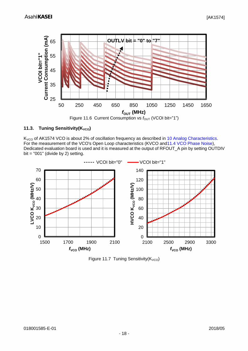
Figure 11.6 Current Consumption vs fOUT (VCOI bit=”1”)
11.3. Tuning Sensitivity(KVCO) KVCO of AK1574 VCO is about 2% of oscillation frequency as described in 10 Analog Characteristics. For the measurement of the VCO's Open Loop characteristics (KVCO and11.4 VCO Phase Noise), Dedicated evaluation board is used and it is measured at the output of RFOUT_A pin by setting OUTDIV bit = "001" (divide by 2) setting.
Figure 11.7 Tuning Sensitivity(KVCO)
25
35
45
55
65
50 250 450 650 850 1050 1250 1450 1650
VC
OI b
it=
"1
"C
urr
en
t C
on
su
mp
tio
n (
mA
)
fOUT (MHz)
OUTLV=0 OUTLV=1 OUTLV=2 OUTLV=3
OUTLV=4 OUTLV=5 OUTLV=6 OUTLV=7
OUTLV bit = "0" to "7"
0
20
40
60
80
100
120
140
2100 2500 2900 3300
HV
CO
KV
CO
(MH
z/V
)
fVCO (MHz)
VCOI bit="0" VCOI bit="1"
0
10
20
30
40
50
60
70
1500 1700 1900 2100
LV
CO
KV
CO
(MH
z/V
)
fVCO (MHz)
VCOI bit=0 VCOI bit=1
0
20
40
60
80
100
120
140
2100 2500 2900 3300
HV
CO
KV
CO
(MH
z/V
)
fVCO (MHz)
VCOI bit=0 VCOI bit=1
[AK1574]
018001585-E-01 2018/05 - 19 -
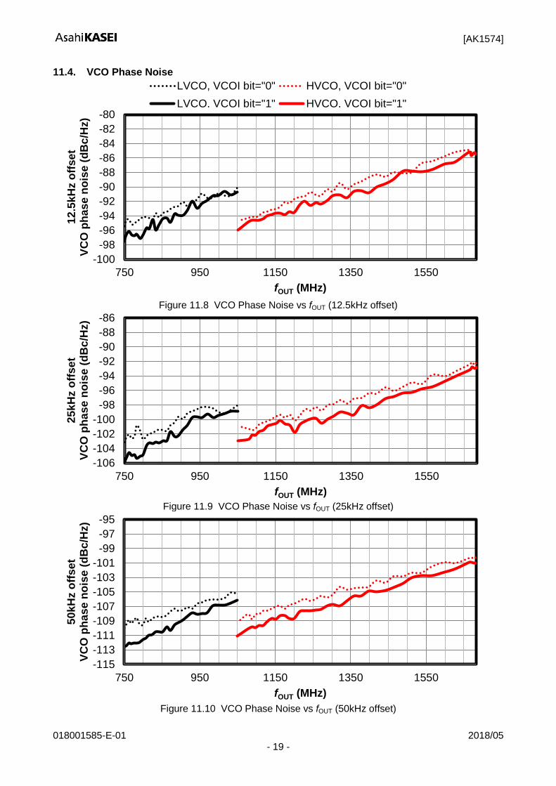
11.4. VCO Phase Noise
Figure 11.8 VCO Phase Noise vs fOUT (12.5kHz offset)
Figure 11.9 VCO Phase Noise vs fOUT (25kHz offset)
Figure 11.10 VCO Phase Noise vs fOUT (50kHz offset)
-100
-98
-96
-94
-92
-90
-88
-86
-84
-82
-80
750 950 1150 1350 1550
Ph
as
e n
ois
e (
dB
c/H
z)
fOUT (MHz)
LVCO, VCOI bit="0" HVCO, VCOI bit="0"
LVCO, VCOI bit="1" HVCO, VCOI bit="1"
-100
-98
-96
-94
-92
-90
-88
-86
-84
-82
-80
750 950 1150 1350 1550
12
.5k
Hz o
ffse
tV
CO
ph
as
e n
ois
e (
dB
c/H
z)
fOUT (MHz)
LVCO at 12.5kHz, VCOI bit="0" HVCO at 12.5kHz, VCOI bit="0"
LVCO at 12.5kHz, VCOI bit="1" HVCO at 12.5kHz, VCOI bit="1"
-106
-104
-102
-100
-98
-96
-94
-92
-90
-88
-86
750 950 1150 1350 1550
25
kH
z o
ffs
et
VC
O p
ha
se
no
ise
(d
Bc
/Hz)
fOUT (MHz)
LVCO at 25kHz, VCOI bit="0" HVCO at 25kHz, VCOI bit="0"
LVCO at 25kHz, VCOI bit="1" HVCO at 25kHz, VCOI bit="1"
-115
-113
-111
-109
-107
-105
-103
-101
-99
-97
-95
750 950 1150 1350 1550
50
kH
z o
ffs
et
VC
O p
ha
se
no
ise
(d
Bc
/Hz)
fOUT (MHz)
LVCO at 50kHz, VCOI bit="0" HVCO at 50kHz, VCOI bit="0"
LVCO at 50kHz, VCOI bit="1" HVCO at 50kHz, VCOI bit="1"
[AK1574]
018001585-E-01 2018/05 - 20 -
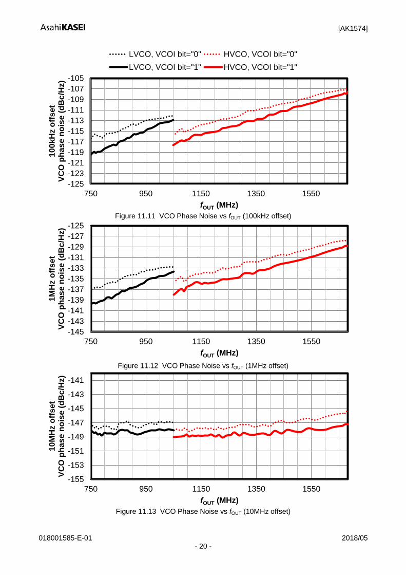
Figure 11.11 VCO Phase Noise vs fOUT (100kHz offset)
Figure 11.12 VCO Phase Noise vs fOUT (1MHz offset)
Figure 11.13 VCO Phase Noise vs fOUT (10MHz offset)
-100
-98
-96
-94
-92
-90
-88
-86
-84
-82
-80
750 950 1150 1350 1550
Ph
as
e n
ois
e (
dB
c/H
z)
fOUT (MHz)
LVCO, VCOI bit="0" HVCO, VCOI bit="0"
LVCO, VCOI bit="1" HVCO, VCOI bit="1"
-125
-123
-121
-119
-117
-115
-113
-111
-109
-107
-105
750 950 1150 1350 1550
10
0k
Hz o
ffse
tV
CO
ph
as
e n
ois
e (
dB
c/H
z)
fOUT (MHz)
LVCO at 100kHz, VCOI bit="0" HVCO at 100kHz, VCOI bit="0"
LVCO at 100kHz, VCOI bit="1" HVCO at 100kHz, VCOI bit="1"
-145
-143
-141
-139
-137
-135
-133
-131
-129
-127
-125
750 950 1150 1350 1550
1M
Hz o
ffse
tV
CO
ph
as
e n
ois
e (
dB
c/H
z)
fOUT (MHz)
LVCO at 1MHz, VCOI bit="0" HVCO at 1MHz, VCOI bit="0"
LVCO at 1MHz, VCOI bit="1" HVCO at 1MHz, VCOI bit="1"
-155
-153
-151
-149
-147
-145
-143
-141
750 950 1150 1350 1550
10
MH
z o
ffs
et
VC
O p
ha
se
no
ise
(d
Bc
/Hz)
fOUT (MHz)
LVCO at 10MHz, VCOI bit="0" HVCO at 10MHz, VCOI bit="0"
LVCO at 10MHz, VCOI bit="1" HVCO at 10MHz, VCOI bit="1"

[AK1574]
018001585-E-01 2018/05 - 21 -
11.5. Closed Loop Phase Noise LVCO is measured when ICP_NORM bit = "10", HVCO is measured when ICP_NORM bit = "01". These values are measured with the same loop filter shown in 15.1 Reference Evaluation Board. CPSRC_I bit is optimized.
Figure 11.14 Closed Loop Phase Noise vs fOUT (LVCO, fVCO=1680MHz)
Figure 11.15 Closed Loop Phase Noise vs fOUT (HVCO, fVCO=3360MHz)
-150
-145
-140
-135
-130
-125
-120
-115
-110
-105
-100
1k 10k 100k 1M 10M
f VC
O=
16
80
MH
zP
ha
se
No
ise
(d
Bc
/Hz)
Offset Frequency (Hz)
OUTDIV=1 OUTDIV=2 OUTDIV=3 OUTDIV=4 OUTDIV=5
fOUT=840MHz
fOUT=420MHz
fOUT=210MHz
fOUT=105MHz
fOUT=52.5MHz
-150
-145
-140
-135
-130
-125
-120
-115
-110
-105
-100
1k 10k 100k 1M 10M
f VC
O=
33
60
MH
zP
ha
se
No
ise
(d
Bc
/Hz)
Offset Frequency (Hz)
OUTDIV=1 OUTDIV=2 OUTDIV=3 OUTDIV=4 OUTDIV=5
fOUT=840MHz
fOUT=420MHz
fOUT=210MHz
fOUT=105MHz
fOUT=1680MHz
[AK1574]
018001585-E-01 2018/05 - 22 -
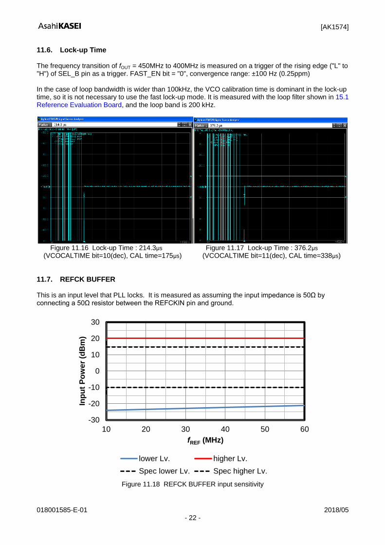
11.6. Lock-up Time The frequency transition of fOUT = 450MHz to 400MHz is measured on a trigger of the rising edge ("L" to "H") of SEL_B pin as a trigger. FAST_EN bit = "0", convergence range: ±100 Hz (0.25ppm) In the case of loop bandwidth is wider than 100kHz, the VCO calibration time is dominant in the lock-up time, so it is not necessary to use the fast lock-up mode. It is measured with the loop filter shown in 15.1 Reference Evaluation Board, and the loop band is 200 kHz.
Figure 11.16 Lock-up Time : 214.3μs Figure 11.17 Lock-up Time : 376.2μs
(VCOCALTIME bit=10(dec), CAL time=175μs) (VCOCALTIME bit=11(dec), CAL time=338μs)
11.7. REFCK BUFFER This is an input level that PLL locks. It is measured as assuming the input impedance is 50Ω by connecting a 50Ω resistor between the REFCKIN pin and ground.
Figure 11.18 REFCK BUFFER input sensitivity
-30
-20
-10
0
10
20
30
10 20 30 40 50 60
Inp
ut
Po
we
r (d
Bm
)
fREF (MHz)
lower Lv. higher Lv.
Spec lower Lv. Spec higher Lv.

[AK1574]
018001585-E-01 2018/05 - 23 -
11.8. REFCK DIVIDER fREF=50.4MHz, REFDIVOUT bit=”10”(Divide by 3=16.8MHz output), REFDIVOUT_POL bit=”0” Input capacitance of measurement probe : 10pF
Figure 11.19 REFCK DIVIDER (50.4MHz/3=16.8MHz output)
11.9. ADC As described in 15.1 Reference Evaluation Board, measured with 1kΩ resistor in series with the MODIN pin for spurious suppression.
Figure 11.20 ADC MODIN pin Input Signal Frequency vs SINAD
55
60
65
70
75
0 10 20 30 40 50
SIN
AD
(d
B)
ADC Input Signal Frequency (kHz)
1k

[AK1574]
018001585-E-01 2018/05 - 24 -
Figure 11.21 ADC MODIN pin Input DC Voltage vs Deviation of fOUT
(fOUT=400MHz, OUTDIV bit=”010”, fPFD=50.4MHz, OFS_DEN bit=all1)
Figure 11.22 ADC MODIN pin Input DC Voltage vs Deviation of fOUT
(MDLT_RATIO bit=”010”, OUTDIV bit=”010”, fPFD=50.4MHz, OFS_DEN bit=all1)
-8
-6
-4
-2
0
2
4
6
8
0 0.5 1 1.5 2 2.5 3
Devia
tion
of f O
UT
(kH
z)
ADC Input Voltage (V)
MDLT_RATIO bit= "0" to "4"
-50
-40
-30
-20
-10
0
10
20
30
40
50
0 0.5 1 1.5 2 2.5 3
Devia
tion
of f O
UT
(kH
z)
ADC Input Voltage (V)
MDLT_RATIO bit= "0" to "4"
-8
-6
-4
-2
0
2
4
6
8
0 0.5 1 1.5 2 2.5 3
Devia
tion
of f O
UT
(kH
z)
ADC Input Voltage (V)
fOUT=400MHz(Divided by 4)
fOUT=470MHz(Divided by 4)(Lines overlap)
[AK1574]
018001585-E-01 2018/05 - 25 -
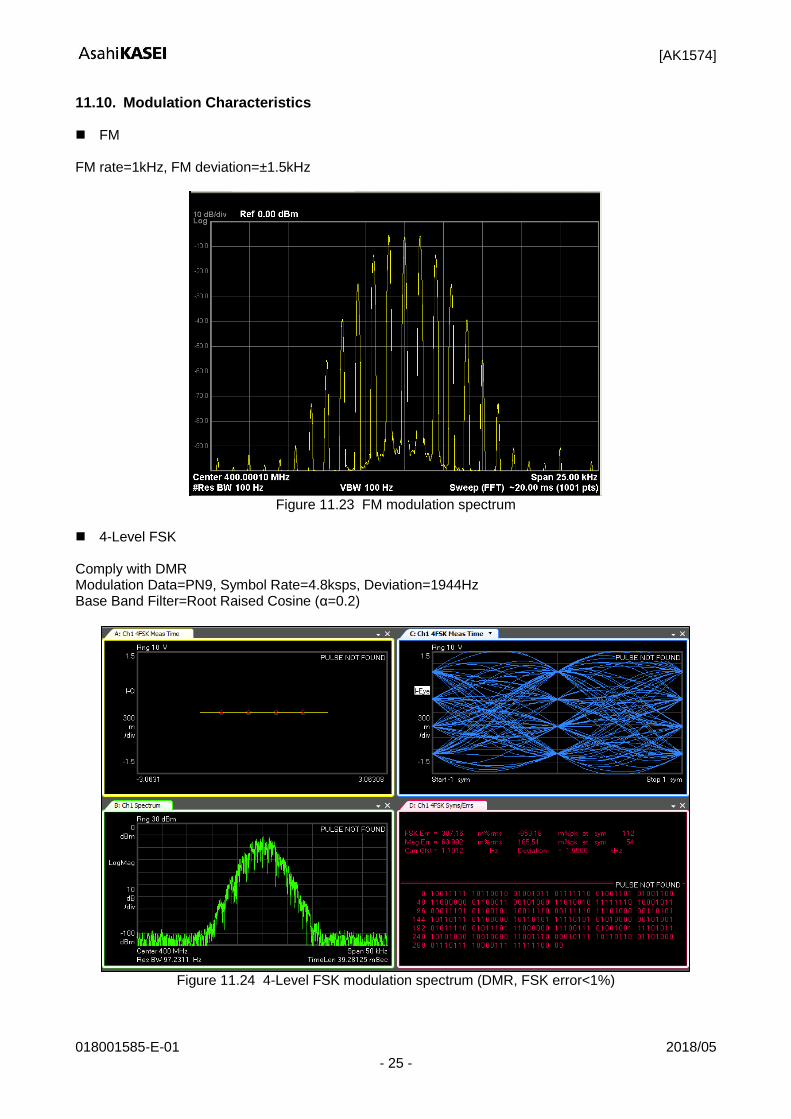
11.10. Modulation Characteristics FM FM rate=1kHz, FM deviation=±1.5kHz
Figure 11.23 FM modulation spectrum
4-Level FSK Comply with DMR Modulation Data=PN9, Symbol Rate=4.8ksps, Deviation=1944Hz Base Band Filter=Root Raised Cosine (α=0.2)
Figure 11.24 4-Level FSK modulation spectrum (DMR, FSK error<1%)

[AK1574]
018001585-E-01 2018/05 - 26 -
11.11. Wide-band Spurious(WBS) Compared to single output, spurious due to the driver amplifier becomes smaller for differential output. Therefore, Differential output is recommended for a low WBS. See also 13.8 Single/Differential Output. Unless otherwise specified, it is measured when ICP_NORM bit="10". By setting lower CP current, the WBS level becomes lower.
Figure 11.25 WBS at REFCK=50.4MHz Figure 11.26 WBS at REFCK=50.4MHz
(Differential Output) (Single Output, OUCAP=33pF)
Figure 11.27 WBS at REFCK=50.4MHz Figure 11.28 WBS at REFCK=50.4MHz (Single Output, OUCAP=33pF+18Ω) (Single Output, OUCAP=33pF+18Ω, ICP_NORM bit=”0”)
[AK1574]
018001585-E-01 2018/05 - 27 -
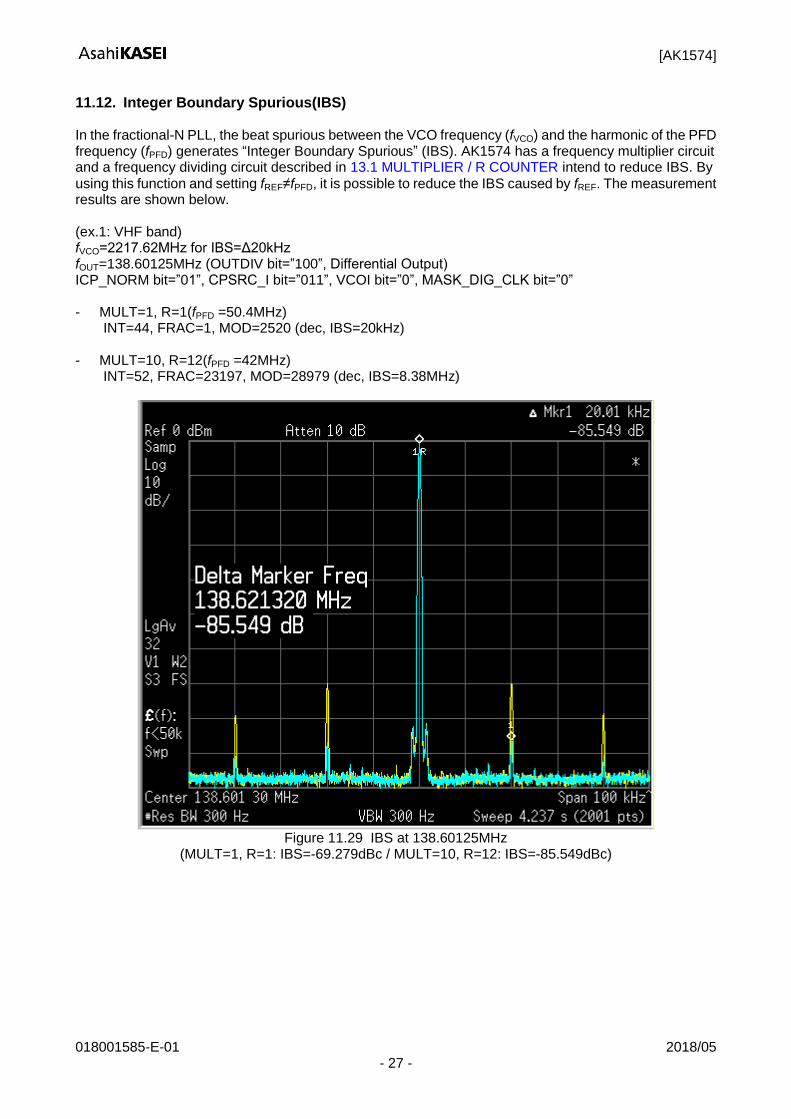
11.12. Integer Boundary Spurious(IBS) In the fractional-N PLL, the beat spurious between the VCO frequency (fVCO) and the harmonic of the PFD frequency (fPFD) generates “Integer Boundary Spurious” (IBS). AK1574 has a frequency multiplier circuit and a frequency dividing circuit described in 13.1 MULTIPLIER / R COUNTER intend to reduce IBS. By using this function and setting fREF≠fPFD, it is possible to reduce the IBS caused by fREF. The measurement results are shown below. (ex.1: VHF band) fVCO=2217.62MHz for IBS=Δ20kHz fOUT=138.60125MHz (OUTDIV bit=”100”, Differential Output) ICP_NORM bit=”01”, CPSRC_I bit=”011”, VCOI bit=”0”, MASK_DIG_CLK bit=”0” - MULT=1, R=1(fPFD =50.4MHz)
INT=44, FRAC=1, MOD=2520 (dec, IBS=20kHz)
- MULT=10, R=12(fPFD =42MHz) INT=52, FRAC=23197, MOD=28979 (dec, IBS=8.38MHz)
Figure 11.29 IBS at 138.60125MHz
(MULT=1, R=1: IBS=-69.279dBc / MULT=10, R=12: IBS=-85.549dBc)

[AK1574]
018001585-E-01 2018/05 - 28 -
(ex.2: UHF band) fVCO=3175.22MHz for IBS=Δ20kHz fOUT=396.9025MHz (OUTDIV bit=”011”, Differential Output) ICP_NORM bit=”01”, CPSRC_I bit=”011”, VCOI bit=”0”, MASK_DIG_CLK bit=”0” - MULT=1, R=1(fPFD =50.4MHz)
INT=63, FRAC=1, MOD=2520 (dec, IBS=20kHz)
- MULT=10, R=12(fPFD =42MHz) INT=75, FRAC=14627, MOD=24359 (dec, IBS=8.38MHz)
Figure 11.30 IBS at 396.9025MHz
(MULT=1, R=1: IBS=-69.629dBc / MULT=10, R=12: IBS=-83.507dBc)
[AK1574]
018001585-E-01 2018/05 - 29 -
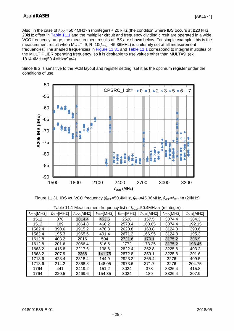
Also, in the case of fVCO =50.4MHz×n (n;integer) + 20 kHz (the condition where IBS occurs at Δ20 kHz, 20kHz offset in Table 11.1 and the multiplier circuit and frequency dividing circuit are operated in a wide VCO frequency range, the measurement results of IBS are shown below. For simple example, this is the measurement result when MULT=9, R=10(fPFD =45.36MHz) is uniformly set at all measurement frequencies. The shaded frequencies in Figure 11.31 and Table 11.1 correspond to integral multiples of the MULTIPLIER operating frequency, so it is desirable to use values other than MULT=9. (ex. 1814.4MHz=(50.4MHz×9)×4) Since IBS is sensitive to the PCB layout and register setting, set it as the optimum register under the conditions of use.
Figure 11.31 IBS vs. VCO frequency (fREF=50.4MHz, fPFD=45.36MHz, fVCO=fREF×n+20kHz)
Table 11.1 Measurement frequency list of fVCO=50.4MHz×n(n;Integer)
fVCO[MHz] fOUT[MHz] fVCO[MHz] fOUT[MHz] fVCO[MHz] fOUT[MHz] fVCO[MHz] fOUT[MHz]
1512 378 1814.4 453.6 2520 157.5 3074.4 384.3
1512 189 1864.8 466.2 2570.4 160.65 3074.4 192.15
1562.4 390.6 1915.2 478.8 2620.8 163.8 3124.8 390.6
1562.4 195.3 1965.6 491.4 2671.2 166.95 3124.8 195.3
1612.8 403.2 2016 504 2721.6 170.1 3175.2 396.9
1612.8 201.6 2066.4 516.6 2772 173.25 3175.2 198.45
1663.2 415.8 2217.6 138.6 2822.4 352.8 3225.6 403.2
1663.2 207.9 2268 141.75 2872.8 359.1 3225.6 201.6
1713.6 428.4 2318.4 144.9 2923.2 365.4 3276 409.5
1713.6 214.2 2368.8 148.05 2973.6 371.7 3276 204.75
1764 441 2419.2 151.2 3024 378 3326.4 415.8
1764 220.5 2469.6 154.35 3024 189 3326.4 207.9
-90
-85
-80
-75
-70
-65
-60
-55
-50
1500 1800 2100 2400 2700 3000 3300
Δ2
0k
IB
S (
dB
c)
fVCO (MHz)
0 1 2 3 5 6 7CPSRC_I bit=
[AK1574]
018001585-E-01 2018/05 - 30 -
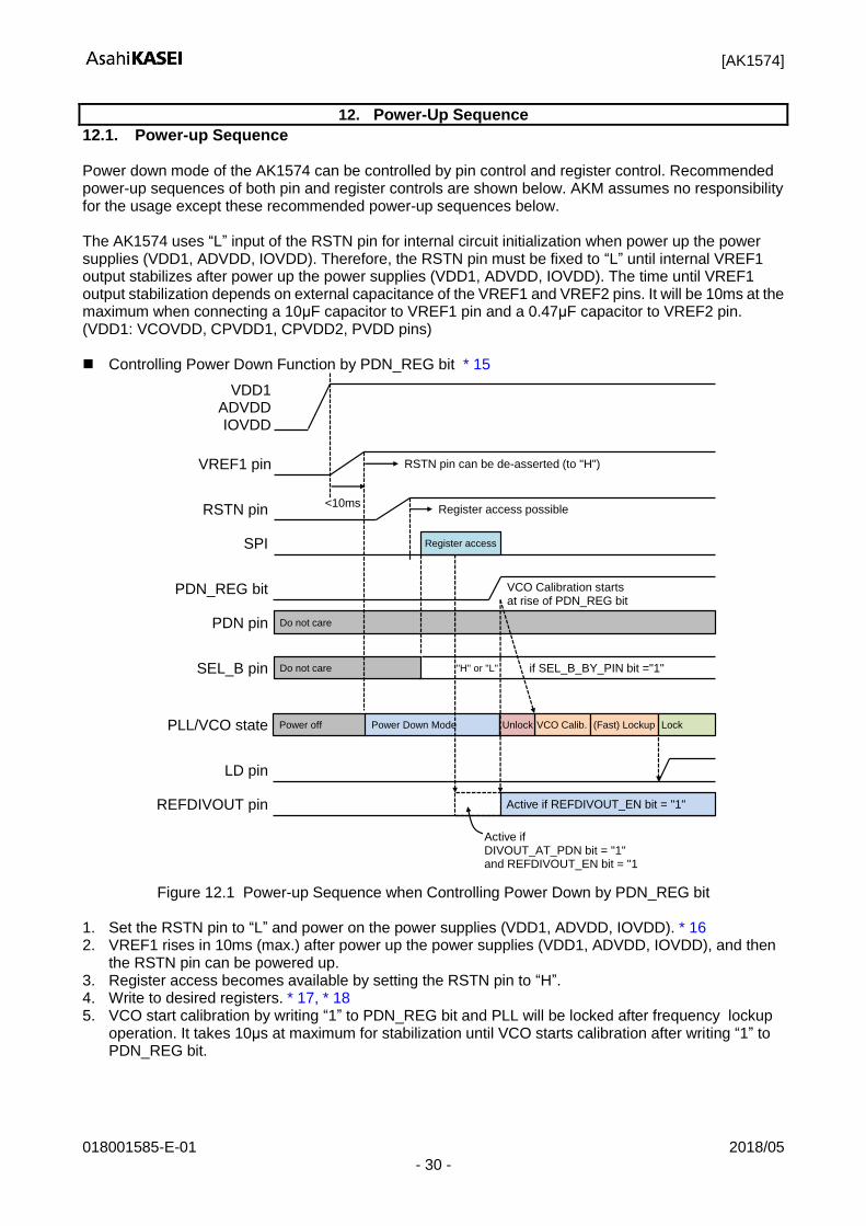
12. Power-Up Sequence
12.1. Power-up Sequence Power down mode of the AK1574 can be controlled by pin control and register control. Recommended power-up sequences of both pin and register controls are shown below. AKM assumes no responsibility for the usage except these recommended power-up sequences below. The AK1574 uses “L” input of the RSTN pin for internal circuit initialization when power up the power supplies (VDD1, ADVDD, IOVDD). Therefore, the RSTN pin must be fixed to “L” until internal VREF1 output stabilizes after power up the power supplies (VDD1, ADVDD, IOVDD). The time until VREF1 output stabilization depends on external capacitance of the VREF1 and VREF2 pins. It will be 10ms at the maximum when connecting a 10μF capacitor to VREF1 pin and a 0.47μF capacitor to VREF2 pin. (VDD1: VCOVDD, CPVDD1, CPVDD2, PVDD pins) Controlling Power Down Function by PDN_REG bit * 15
Figure 12.1 Power-up Sequence when Controlling Power Down by PDN_REG bit
1. Set the RSTN pin to “L” and power on the power supplies (VDD1, ADVDD, IOVDD). * 16 2. VREF1 rises in 10ms (max.) after power up the power supplies (VDD1, ADVDD, IOVDD), and then
the RSTN pin can be powered up. 3. Register access becomes available by setting the RSTN pin to “H”. 4. Write to desired registers. * 17, * 18 5. VCO start calibration by writing “1” to PDN_REG bit and PLL will be locked after frequency lockup
operation. It takes 10μs at maximum for stabilization until VCO starts calibration after writing “1” to PDN_REG bit.
Do not care
VDD1ADVDDIOVDD
VREF1 pin
SPI Register access
Power off Power Down Mode
RSTN pin can be de-asserted (to "H")
VCO Calib. (Fast) Lockup LockUnlock
VCO Calibration startsat rise of PDN_REG bit
RSTN pin Register access possible
PDN_REG bit
PDN pin
PLL/VCO state
SEL_B pin Do not care if SEL_B_BY_PIN bit ="1""H" or "L"
REFDIVOUT pin
Active if DIVOUT_AT_PDN bit = "1"and REFDIVOUT_EN bit = "1
Active if REFDIVOUT_EN bit = "1"
<10ms
LD pin

[AK1574]
018001585-E-01 2018/05 - 31 -
Notes: * 15. Input signal of the PDN pin when controlling power down mode by PDN_REG bit is “Do not care”.
Refer to Table 14.1 for detail. PDN_BY_PIN bit must be fixed to “0” until the power-up sequence finishes (until PLL frequency is locked).
* 16. Power-up sequence between VDD1, ADVDD and IOVDD is not critical. VREF1 output is stabilized in 10ms (max.) after all power supplies are on.
* 17. Divided reference clock is output from the REFDIVOUT pin when setting REFDIVOUT_EN bit to “1”. The REFDIVOUT pin output will be “L” if REFDIVOUT_EN bit is not “1”.
* 18. The input signal to the SEL_B pin should be fixed to “L” or “H” until power-up sequence is finished (until PLL frequency is locked) when setting SEL_B_BY_PIN bit to “1”. The input signal of the SEL_B pin is “Do not care” if SEL_B_BY_PIN bit is not “1”.
Controlling Power Down Function by PDN pin * 19
Figure 12.2 Power-up Sequence when Controlling Power Down by PDN pin
1. Set the RSTN pin to “L” and power on the power supplies (VDD1, ADVDD, IOVDD). * 20 2. VREF1 rises in 10ms (max.) after power up the power supplies (VDD1, ADVDD, IOVDD), and then
RSTN pin can be powered up. 3. Register access becomes available by setting the RSTN pin to “H”. 4. Write to desired registers. * 21, * 22
At this timing, set the PDN pin to “L” and PDN_BY_PIN bit to “1”. Power Down function is controlled by the PDN pin when setting PDN_BY_PIN bit = “1”.
5. VCO start calibration by setting the PDN pin to “H” and PLL will be locked after frequency lockup operation. It takes 10μs at maximum for stabilization until VCO starts calibration after setting the PDN pin to “H”.
Do not care
VDD1ADVDDIOVDD
VREF1 pin
SPI
<10ms
Register access
Power off Power Down Mode
RSTN pin can be de-asserted (to "H")
VCO Calib. (Fast) Lockup LockUnlock
VCO Calibration startsat rise of PDN pin
RSTN pin
PDN_BY_PIN bit ="1"
Register access possible
PDN_REG bit
PDN pin
PLL/VCO state
SEL_B pin if SEL_B_BY_PIN bit ="1""H" or "L"
REFDIVOUT pin
Active if DIVOUT_AT_PDN bit = "1"and REFDIVOUT_EN bit = "1
Active if REFDIVOUT_EN bit = "1"
Do not care
LD pin

[AK1574]
018001585-E-01 2018/05 - 32 -
Notes: * 19. Write “1” to PDN_BY_PIN bit in the timing shown in Figure 12.2. PDN_REG bit is “Do not care” when
PDN_BY_PIN bit is “1”. * 20. Power-up sequence between VDD1, ADVDD and IOVDD is not critical. VREF1 output is stabilized in
10ms (max.) after all power supplies are on. * 21. Divided reference clock is output from the REFDIVOUT pin when setting REFDIVOUT_EN bit to “1”.
The REFDIVOUT pin output will be “L” if REFDIVOUT_EN bit is not “1”. * 22. The input signal to the SEL_B pin should be fixed to “L” or “H” until power-up sequence is finished
(until PLL frequency is locked) when setting SEL_B_BY_PIN bit to “1”. The input signal of the SEL_B pin is “Do not care” if SEL_B_BY_PIN bit is not “1”.
[AK1574]
018001585-E-01 2018/05 - 33 -
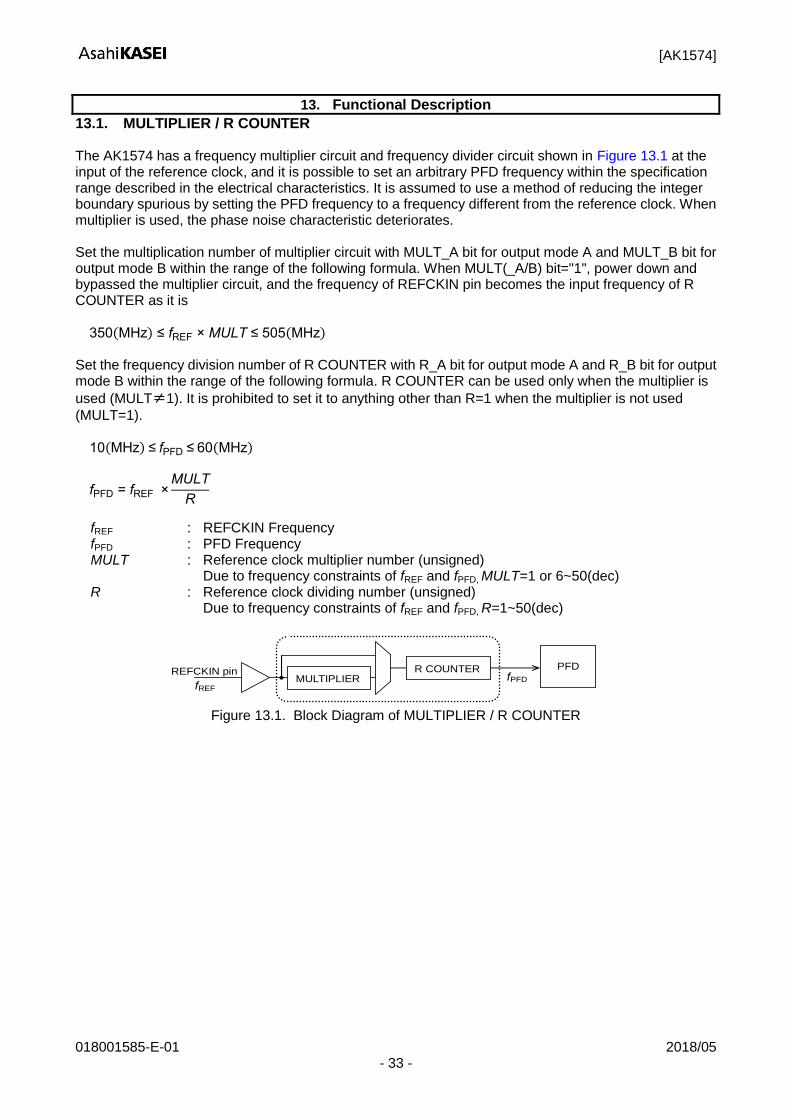
13. Functional Description
13.1. MULTIPLIER / R COUNTER The AK1574 has a frequency multiplier circuit and frequency divider circuit shown in Figure 13.1 at the input of the reference clock, and it is possible to set an arbitrary PFD frequency within the specification range described in the electrical characteristics. It is assumed to use a method of reducing the integer boundary spurious by setting the PFD frequency to a frequency different from the reference clock. When multiplier is used, the phase noise characteristic deteriorates. Set the multiplication number of multiplier circuit with MULT_A bit for output mode A and MULT_B bit for output mode B within the range of the following formula. When MULT(_A/B) bit="1", power down and bypassed the multiplier circuit, and the frequency of REFCKIN pin becomes the input frequency of R COUNTER as it is
350(MHz) ≤ fREF × MULT ≤ 505(MHz) Set the frequency division number of R COUNTER with R_A bit for output mode A and R_B bit for output mode B within the range of the following formula. R COUNTER can be used only when the multiplier is
used (MULT≠1). It is prohibited to set it to anything other than R=1 when the multiplier is not used
(MULT=1).
10(MHz) ≤ fPFD ≤ 60(MHz)
fPFD = fREF ×MULT
R
fREF : REFCKIN Frequency fPFD : PFD Frequency MULT : Reference clock multiplier number (unsigned) Due to frequency constraints of fREF and fPFD, MULT=1 or 6~50(dec) R : Reference clock dividing number (unsigned) Due to frequency constraints of fREF and fPFD, R=1~50(dec)
REFCKIN pin
MULTIPLIER
R COUNTER PFD
fREF
fPFD
Figure 13.1. Block Diagram of MULTIPLIER / R COUNTER
[AK1574]
018001585-E-01 2018/05 - 34 -
13.2. Frequency Stetting VCO frequency and the Output Frequency of the AK1574 are calculated by the following formula.
fVCO=fPFD × (INT+FRAC
MOD+
MDLT_RATIO × (pol × OFS_MDLT+modulation)+OFS_FINE
OFS_DEN)
fOUT=fVCO
OUTDIV
Following Words Indicate INT: Integer Portion of Dividing Value
Set within the range 28 ≤ INT ≤ 336 (dec) (unsigned, 9bits) In Output Mode A, it is a setting value of INT_A bits. In Output Mode B, it is a setting value of INT_B bits. Refer to Table 13.2 for details of Output Mode A and B. FRAC: Numerator for Fractional Portion of Dividing Value
Set within the range 0 ≤ FRAC <MOD (dec) (unsigned, 15bits) In Output Mode A, it is a setting value of FRAC_A bits. In Output Mode B, it is a setting value of FRAC_B bits. MOD: Denominator for Fractional Portion of Dividing Value
Set within the range 2 ≤ MOD ≤ 32767 (dec) (unsigned, 15bits) In Output Mode A, it is a setting value of MOD_A bits. In Output Mode B, it is a setting value of MOD_B bits. MDLT_RATIO: Step Ratio of OFS_FINE to Modulation Signal (modulation and OFS_MDLT) It is used to keep OFS_FINE accuracy while getting wide modulation. Refer to Table 14.5 for setting. In Output Mode A, it is a assigned value of MDLT_RATIO_A bits. In Output Mode B, it is a assigned value of MDLT_RATIO_B bits.
OFS_FINE: Finest Adjustment (1LSB = fPFD/OFS_DEN) of Frequency Offset Set within the range -2048(0x800) ~ +2047(0x7FF) (signed, 12bits)
It is used for trimming a frequency shift of TCXO when shipping user’s product. In Output Mode A, it is a setting value of OFS_FINE_A bits. In Output Mode B, it is a setting value of OFS_FINE_B bits.
When spurious occurs in the output signal, set it to avoid 0, negative odd number and positive even number. This eliminates the periodicity of internal operation, which may improve spurious. At this time, it is recommended to set the maximum value (all 1) for OFS_DEN.
OFS_MDLT: Coarse Adjustment (MDLT_RATIO times comparing to OFS_FINE) of Frequency Offset Set within the range -2048(0x800) ~ +2047(0x7FF) (signed, 12bits) It is used for FM/FSK modulation and to shift a specific frequency in direct conversion.
In Output Mode A, it is a setting value of OFS_MDLT_A bits. In Output Mode B, it is a setting value of OFS_MDLT_B bits.
OFS_DEN: Frequency Offset Value (OFS_FINE, OFS_MDLT) and Denominator of Modulation Input(modulation) (unsigned, 23bits) The setting value should be larger than 1 and satisfy the (Eq. 14.2).
In Output Mode A, it is a setting value of OFS_DEN_A bits. In Output Mode B, it is a setting value of OFS_DEN_B bits. This bit is recommended to set the maximum value (all 1) pol: FREQ_POL pin = “L” : +1 FREQ_POL pin = “H” : -1
modulation: Modulation Signal. A/D conversion result by inputting analog modulation signal or digital modulation input value

[AK1574]
018001585-E-01 2018/05 - 35 -
OUTDIV: Output Dividing Value In Output Mode A, it is a setting value of OUTDIV_A bits. In Output Mode B, it is a setting value of OUTDIV_B bits. and there are three following limitations for frequency setting range. VCO Frequency with No-modulation (caused by limitation of the VCO frequency range)
1500 MHz ≤ fPFD × (INT+FRAC
MOD+
OFS_FINE
OFS_DEN) ≤ 2100 MHz
(when HVCO_SEL(_A/B) bit = “0”)
2100 MHz ≤ fPFD × (INT+FRAC
MOD+
OFS_FINE
OFS_DEN) ≤ 3365 MHz
(when HVCO_SEL(_A/B) bit = “1” )
Offset + Modulation Value (caused by limitation of the VCO frequency range that is operable without re-executing VCOCAL)
|MDLT_RATIO × (pol × OFS_MDLT +modulation)
OFS_DEN| <0.001 × (INT+
FRAC
MOD+
OFS_FINE
OFS_DEN)
(Deviation from VCO Frequency with VCOCAL < ±0.1%) Fractional Signal Range (caused by a range of delta-sigma modulator value)
|MDLT_RATIO × (pol × OFS_MDLT +modulation)+OFS_FINE
OFS_DEN| <0.5
For example, fVCO=2000MHz, OUTDIV=4 satisfies conditions of No-modulation when fPFD=52MHz and fOUT=500MHz. The setting will be as below.
INT = 38 FRAC/MOD = 12/26 OUTDIV = 4
In the case of modulation input is ±512code (ADVDD/4 Vp-p), a desired frequency deviation is ±3kHz and frequency shift of TCXO is +1ppm (+500Hz with 500MHz output)
Frequency deviation of VCO is ±12 kHz since OUTDIV=4, therefore it will be 12000/512 Hz/LSB. Since fPFD=52MHz,
OFS_DEN=MDLT_RATIO × fPFD
fLSB
=MDLT_RATIO × 52000000
12000/512=MDLT_RATIO × 2218667
The maximum MDLT_RATIO is 2 because “OFS_DEN < 2
23 = 8,388,608”. OFS_DEN=4,437,334
In this case, it is able to compensate residual frequency error up to “500 - 171*2.93 = -0.977Hz (-0.0020ppm)” assuming OFS_FINE=171 since OFS_FINE holds “52MHz / 4,437,333 / 4(OUTDIV)/ LSB = 2.93Hz (0.0059ppm) /LSB”. Frequency error compensation of the AK1574 is carried by adding fixed value to VCO frequency instead of calculating by ratio of fPFD. Residual frequency error will become larger if the VCO frequency differs away from the compensatory range by OFS_DEN (Table 13.1).

[AK1574]
018001585-E-01 2018/05 - 36 -
Table 13.1 Error of Residue f per 1ppm after Compensation
fOUT
[MHz] OUT DIV
fVCO [MHz]
VCO fERROR [Hz]
OFS_FINE Correction[Hz]
Residue VCO fERROR [Hz]
Residue fERROR [ppm]
1050 2 2100 +2100 -2004 +96 +0.05
751 2 1502 +1502 -2004 -502 -0.33
749 4 2996 +2996 -2004 +992 +0.33
550 4 2200 +2200 -2004 +196 0.09
500 4 2000 +2000 -2004 -4 0.00
450 4 1800 +1800 -2004 -204 -0.11
376 4 1504 +1504 -2004 -500 -0.33
374 8 2992 +2992 -2004 +988 +0.33
188 8 1504 +1504 -2004 -500 -0.33
187 16 2992 +2992 -2004 +988 +0.33
94 16 1504 +1504 -2004 -500 -0.33
93 32 2976 +2976 -2004 +972 +0.33
50 32 1600 +1600 -2004 -404 -0.25
A/B Output Mode Switching The AK1574 has two setting modes “A” and “B” for easy switching of operation mode such as transmitting/receiving and etc. These modes can be controlled by the SEL_B pin or SEL_B_REG bit. "A" and "B" modes switching logic is shown below.
Table 13.2 A/B Output Mode Switching Logic
SEL_B_BY_PIN bit SEL_B_REG bit SEL_B pin Output Mode
0 0 X A
0 1 X B
1 X L A
1 X H B
"A" and "B" mode setting contents are as below.
Table 13.3 A/B Mode Switching Parameters
Category A B Description
Frequency FRAC_A FRAC_B Fractional Portion Numerator of Dividing Value, unsigned, 15bits
MOD_A MOD_B Fractional Portion Denominator of Dividing Value, unsigned, 15bits
INT_A INT_B Integer Portion or Dividing Value, unsigned, 9bits
HVCO_SEL_A HVCO_SEL_B VCO Range Switching
OUTDIV_A OUTDIV_B Output Divider
MDLT_RATIO_A MDLT_RATIO_B Modulation/ OFS_FINE Ratio
OFS_FINE_A OFS_FINE_B Fine Offset, signed, 12bits
OFS_MDLT_A OFS_MDLT_B Modulation Offset, signed, 12bits
OFS_DEN_A OFS_DEN_B Modulation/Offset Denominator, unsigned, 23bits
MULT_A MULT_B Multiplying Number of REFCK Frequency
R_A R_B Dividing Number of REFCK Frequency
Modulation MOD_EN_A MOD_EN_B Modulation Circuit Enable
MOD_NULL_A MOD_NULL_B 0 fixed Modulation Value
MOD_ADC_A MOD_ADC_B Modulation at Analog Input
Output OUTA_REG_A OUTA_REG_B RFOUT_A Valid
OUTB_REG_A OUTB_REG_B RFOUT_B Valid
OUTLV_A OUTLV_B RFOUT Level
[AK1574]
018001585-E-01 2018/05 - 37 -
When switching mode A/B, VCO is re-locked up. Even if modes “A” and “B” have the same frequency setting, VCO will be locked up again. When mode “A” is selected, VCO is also locked up by writing to FRAC, MOD, INT, MULT, R, HVCO_SEL, OUTDIV_A bits but it is not locked up by writing to FRAC, MOD, INT, MULT, R, HVCO_SEL, OUTDIV_B bits.
13.3. Re-lock up event In the AK1574, the VCO starts calibration with one of the following operations (hereinafter referred to as a re-lockup event) as a trigger, and the PLL locks after frequency lockup operation. Re-setting frequency (generating a new re-lock up event) is prohibited until completing VCO calibration and finishing fast lock-up mode after a generation of re-lock up event. Refer to 13.5 VCO for VCO calibration. Refer to 13.4 Fast Lock-Up Mode for Fast Lock-Up Mode. Power Down Release
- Change the PDN pin state “L” to “H” while PDN_BY_PIN bit = “1” - Set PDN_REG bit “0” to “1” while PDN_BY_PIN bit = “0” - PDN signal is changed as “L”(“0”) to “H”(“1”) by changing PDN_BY_PIN bit setting.
A/B Mode Switching - Change the SEL_B pin status while SEL_B_BY_PIN bit = “1” - Change SEL_B_REG bit setting while SEL_B_BY_PIN bit = “0” - SEL_B signal is changed by changing SEL_B_BY_PIN bit setting.
Frequency Change - Write to the register address 0x07 when the AK1574 is in mode “A” - Write to the register address 0x17 when the AK1574 is in mode “B” Even if the same frequency setting is written again, it will be locked up again.
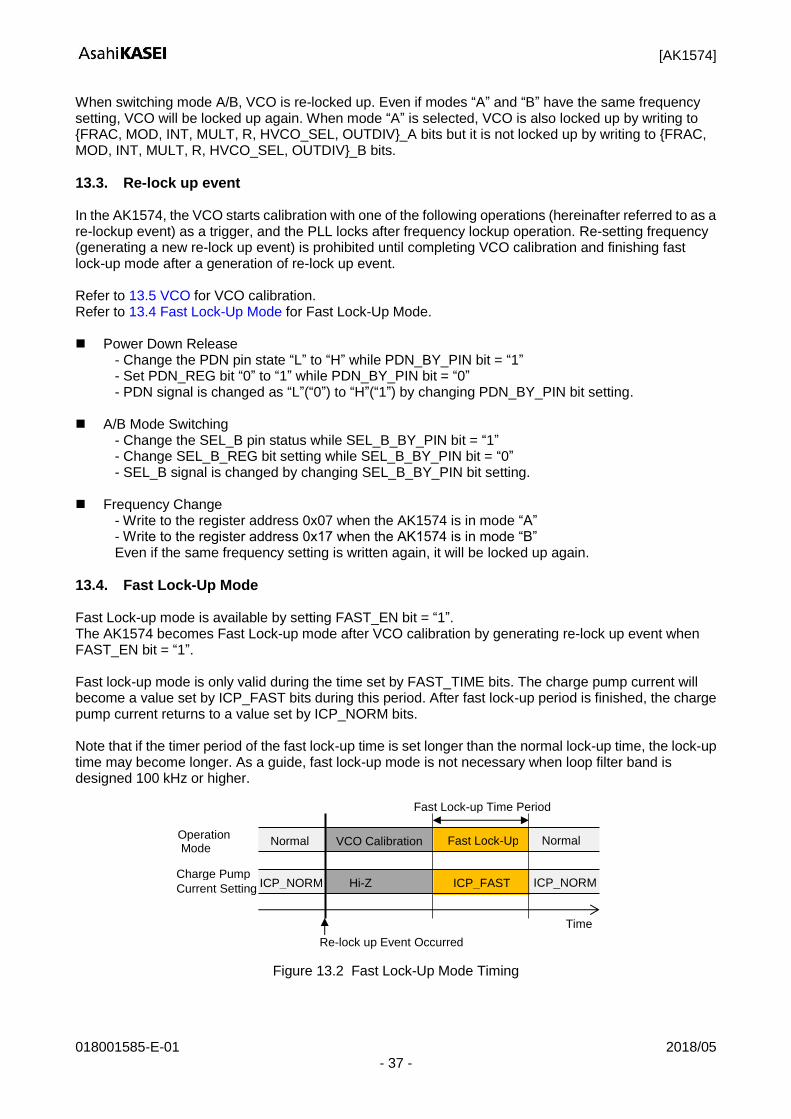
13.4. Fast Lock-Up Mode Fast Lock-up mode is available by setting FAST_EN bit = “1”. The AK1574 becomes Fast Lock-up mode after VCO calibration by generating re-lock up event when FAST_EN bit = “1”. Fast lock-up mode is only valid during the time set by FAST_TIME bits. The charge pump current will become a value set by ICP_FAST bits during this period. After fast lock-up period is finished, the charge pump current returns to a value set by ICP_NORM bits. Note that if the timer period of the fast lock-up time is set longer than the normal lock-up time, the lock-up time may become longer. As a guide, fast lock-up mode is not necessary when loop filter band is designed 100 kHz or higher.
Figure 13.2 Fast Lock-Up Mode Timing
Normal Fast Lock-Up Normal
ICP_NORM ICP_FAST ICP_NORM Charge Pump Current Setting
Re-lock up Event Occurred
Operation Mode
Fast Lock-up Time Period
VCO Calibration
Hi-Z
Time
[AK1574]
018001585-E-01 2018/05 - 38 -
Fast lock-up time period is set by PFD cycle(TPFD) × (1023 + 1024 × FAST_TIME). Setting examples are shown in Table 13.4.
Table 13.4 Fast Lock-Up Period
FAST_TIME decimal
Duration [µs] at 60MHz PFD
Duration [µs] at 10MHz PFD
0 17 102
1 34 205
2 51 307
3 68 410
4 85 512
5 102 614
6 119 717
7 137 819
8 154 922
9 171 1024
10 188 1126
11 205 1229
12 222 1331
13 239 1434
14 256 1536
15 273 1638
13.5. VCO
VCO Calibration VCO frequency band of AK1574 is divided into multiple bands to realize low-phase noise, low sensitivity and broad frequency range. The AK1574 executes calibration to select the best band when setting the frequency. VCO calibration is executed as..
fPFD × ∙ (INT+FRAC
MOD+
OFS_FINE
OFS_DEN)
Note that OFS_FINE registers are effective to the VCO calibration. VCO calibration starts by13.3 Re-lock up event. The control voltage is shutout internally during a calibration and the internal reference voltage is connected. The charge pump output will be Hi-Z state and LD pin becomes unlock ("L" output) during a calibration. The internal bias must be stable to execute a calibration correctly. Since the AK1574 waits this stabilization time of the internal bias when power-down is released, the calibration time is different when power-down is released and other situations when re-lock up event is occurred. VCO calibration time depends on VCOCAL_TIME bits setting. When VCOCAL_TIME bits setting value is increased, VCO calibration accuracy is increased but also VCO calibration time is increased. It is recommended to use a value calculated by the formula (Eq. 13.1) for VCOCAL_TIME bits setting to obtain sufficient VCO calibration accuracy. However, VCOCAL_TIME bits (dec) must be in the range from 1 to 11. It is designed to set 7 (dec) when a prohibited value is input, but the value is not guaranteed. It is prohibited to set 0 or a value more than 11. By setting the VCOCAL_TIME bit to a value smaller than the recommended value, it may VCO is to unlock.
VCOCAL_TIME bit ≥ log2(fPFD/50000) (Eq. 13.1)
VCO calibration time is calculated approximately as below.
VCO calibration time TPFD × ( (6 + 2 ^ VCOCAL_TIME bit) × 8 + 3) + TREF × 600 (256 × TPFD are added when released power-down mode)
Generating a new re-lock up event is prohibited until completing VCO calibration and finishing fast lock-up mode after a generation of re-lock up event.

[AK1574]
018001585-E-01 2018/05 - 39 -
Low-Phase Noise Mode The AK1574 operates low-phase noise mode by setting VCOI bit to “1” and then VCO current is increased. The power consumption in low-phase noise mode is increased comparing to low power mode with VCOI bit=”0”.
13.6. LOOP FILTER Figure 13.3 shows an example of the configuration of an external loop filter for PLL stabilization. The AK1574 is mainly intended for use in narrow band applications. So the constants described on the15.1 Reference Evaluation Board are designed to reduce the In-band Phase Noise of ~100kHz offset by designing the loop band to 100kHz or more. In order to suppress fractional noise which becomes larger more than 1MHz offset, it is a third order loop filter. In addition, PLL design tool is also provided for design support of arbitrary loop filter constants. https://www.akm.com/akm/en/product/detail/0038/
C2
C1 C3 R2
R3
CPOUT to VCNT pin
Figure 13.3 Example of an external loop filter
[AK1574]
018001585-E-01 2018/05 - 40 -
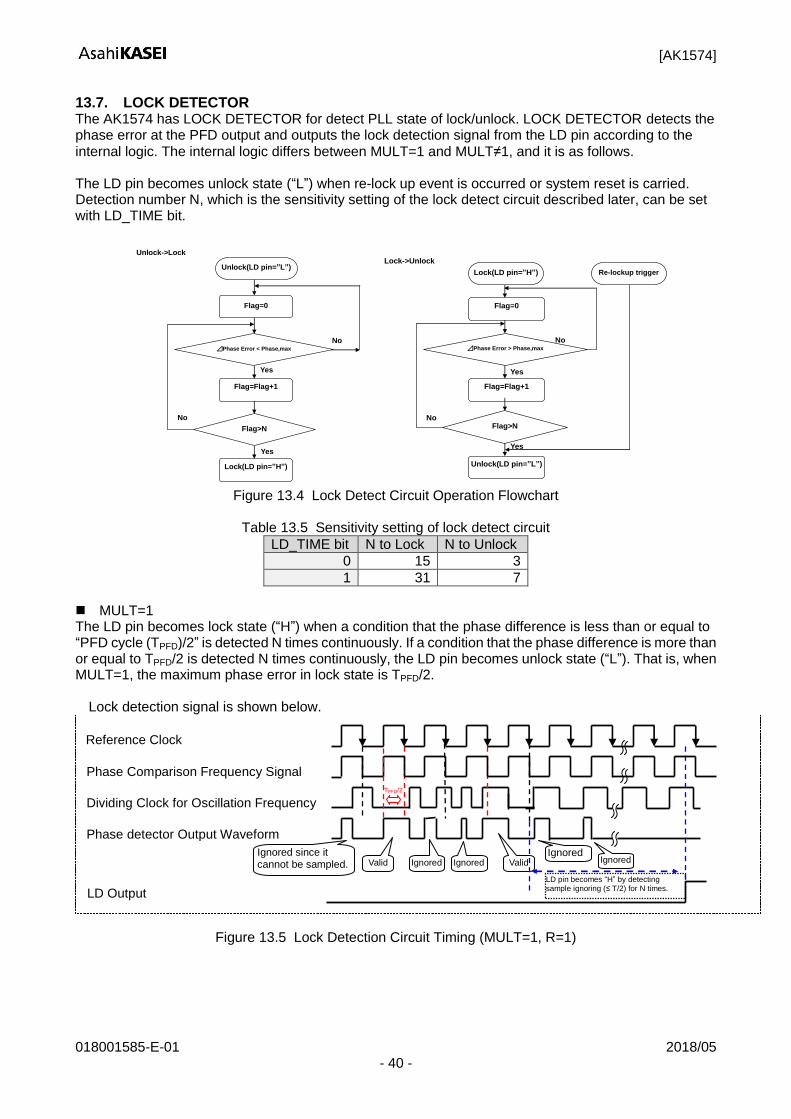
13.7. LOCK DETECTOR The AK1574 has LOCK DETECTOR for detect PLL state of lock/unlock. LOCK DETECTOR detects the phase error at the PFD output and outputs the lock detection signal from the LD pin according to the internal logic. The internal logic differs between MULT=1 and MULT≠1, and it is as follows. The LD pin becomes unlock state (“L”) when re-lock up event is occurred or system reset is carried. Detection number N, which is the sensitivity setting of the lock detect circuit described later, can be set with LD_TIME bit.
⊿Phase Error < Phase,max
Flag=Flag+1
Lock(LD pin=”H”)
Unlock(LD pin=”L”)
Yes
No
Flag>N
Flag=0
Yes
No
Unlock->Lock
⊿Phase Error > Phase,max
Yes
Flag=0
Flag=Flag+1
Flag>N No
Yes
Unlock(LD pin=”L”)
No
Lock->Unlock
Lock(LD pin=”H”) Re-lockup trigger
Figure 13.4 Lock Detect Circuit Operation Flowchart
Table 13.5 Sensitivity setting of lock detect circuit
LD_TIME bit N to Lock N to Unlock
0 15 3
1 31 7
MULT=1 The LD pin becomes lock state (“H”) when a condition that the phase difference is less than or equal to “PFD cycle (TPFD)/2” is detected N times continuously. If a condition that the phase difference is more than or equal to TPFD/2 is detected N times continuously, the LD pin becomes unlock state (“L”). That is, when MULT=1, the maximum phase error in lock state is TPFD/2.
Lock detection signal is shown below.
Reference Clock
Ignored since it cannot be sampled. Valid
Phase Comparison Frequency Signal
Dividing Clock for Oscillation Frequency
Phase detector Output Waveform
Valid Ignored
LD Output
LD pin becomes “H” by detecting sample ignoring (≤ T/2) for N times.
Ignored Ignored
TPFD/2
/2
Ignored
Figure 13.5 Lock Detection Circuit Timing (MULT=1, R=1)

[AK1574]
018001585-E-01 2018/05 - 41 -
MULT ≠1 LD pin becomes "H" (lock) when the phase error is continuously detected N times with the TMULT×4 or less. TMULT is the period of the output of the MULTIPLIER. In this state, LD pin becomes "L" (unlock) if phase error TMULT×4 or more is continuously detected N times. That is, when MULT≠1, the maximum phase error in lock state is TMULT×4. For circuit operation, as shown in Figure 13.6, a lock window with a width of TMULT×5 is generated with reference to the rising edge of the phase comparator output. Then, lock detect circuit detects whether the rising edge of the division clock of the VCO is in the lock window or not.
Figure 13.6 Lock Detection Circuit Timing (MULT≠1, ex: MULT=8, R=9)
Reference Clock
MULTIPLIER Output
Phase Comparison Frequency
Dividing Clock of VCO Frequency
Lock window
TMULT×4CLK
TMULT×1CLK
[AK1574]
018001585-E-01 2018/05 - 42 -
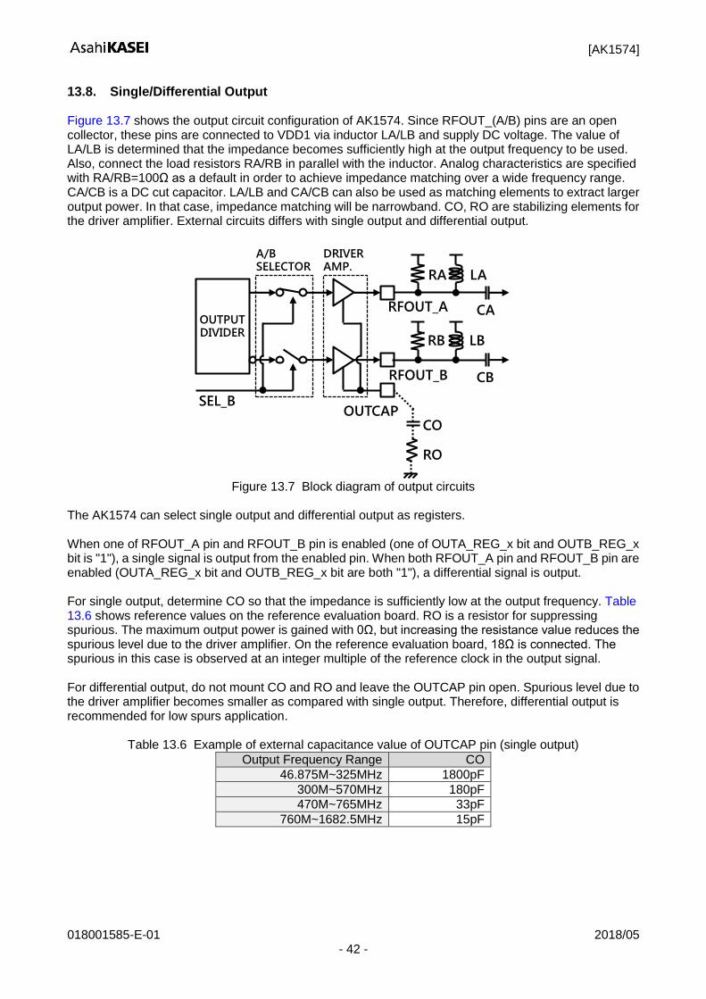
13.8. Single/Differential Output Figure 13.7 shows the output circuit configuration of AK1574. Since RFOUT_(A/B) pins are an open collector, these pins are connected to VDD1 via inductor LA/LB and supply DC voltage. The value of LA/LB is determined that the impedance becomes sufficiently high at the output frequency to be used. Also, connect the load resistors RA/RB in parallel with the inductor. Analog characteristics are specified with RA/RB=100Ω as a default in order to achieve impedance matching over a wide frequency range. CA/CB is a DC cut capacitor. LA/LB and CA/CB can also be used as matching elements to extract larger output power. In that case, impedance matching will be narrowband. CO, RO are stabilizing elements for the driver amplifier. External circuits differs with single output and differential output.
Figure 13.7 Block diagram of output circuits
The AK1574 can select single output and differential output as registers. When one of RFOUT_A pin and RFOUT_B pin is enabled (one of OUTA_REG_x bit and OUTB_REG_x bit is "1"), a single signal is output from the enabled pin. When both RFOUT_A pin and RFOUT_B pin are enabled (OUTA_REG_x bit and OUTB_REG_x bit are both "1"), a differential signal is output. For single output, determine CO so that the impedance is sufficiently low at the output frequency. Table 13.6 shows reference values on the reference evaluation board. RO is a resistor for suppressing spurious. The maximum output power is gained with 0Ω, but increasing the resistance value reduces the spurious level due to the driver amplifier. On the reference evaluation board, 18Ω is connected. The spurious in this case is observed at an integer multiple of the reference clock in the output signal. For differential output, do not mount CO and RO and leave the OUTCAP pin open. Spurious level due to the driver amplifier becomes smaller as compared with single output. Therefore, differential output is recommended for low spurs application.
Table 13.6 Example of external capacitance value of OUTCAP pin (single output)
Output Frequency Range CO
46.875M~325MHz 1800pF
300M~570MHz 180pF
470M~765MHz 33pF
760M~1682.5MHz 15pF
OUTPUTDIVIDER
DRIVERAMP.
RFOUT_B
RFOUT_A
OUTCAP
A/BSELECTOR
SEL_B
RA LA
RB LB
RO
CO
CA
CB
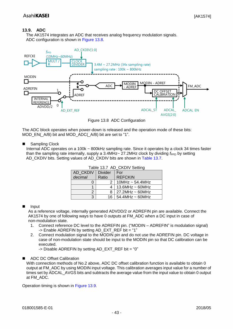
[AK1574]
018001585-E-01 2018/05 - 43 -
13.9. ADC The AK1574 integrates an ADC that receives analog frequency modulation signals. ADC configuration is shown in Figure 13.8.
Figure 13.8 ADC Configuration
The ADC block operates when power-down is released and the operation mode of these bits: MOD_EN(_A/B) bit and MOD_ADC(_A/B) bit are set to “1”. Sampling Clock
Internal ADC operates on a 100k ~ 800kHz sampling rate. Since it operates by a clock 34 times faster than the sampling rate internally, supply a 3.4MHz~ 27.2MHz clock by dividing fPFD by setting AD_CKDIV bits. Setting values of AD_CKDIV bits are shown in Table 13.7.
Table 13.7 AD_CKDIV Setting
AD_CKDIV decimal
Divider Ratio
For REFCKIN
0 2 10MHz ~ 54.4MHz
1 4 13.6MHz ~ 60MHz
2 8 27.2MHz ~ 60MHz
3 16 54.4MHz ~ 60MHz
Input
As a reference voltage, internally generated ADVDD/2 or ADREFIN pin are available. Connect the AK1574 by one of following ways to have 0 outputs at FM_ADC when a DC input in case of non-modulation state. 1. Connect reference DC level to the ADREFIN pin. (“MODIN – ADREFIN” is modulation signal)
-> Enable ADREFIN by setting AD_EXT_REF bit = “1” 2. Connect modulation signal to the MODIN pin and do not use the ADREFIN pin. DC voltage in
case of non-modulation state should be input to the MODIN pin so that DC calibration can be executed. -> Disable ADREFIN by setting AD_EXT_REF bit = “0”
ADC DC Offset Calibration
With connection methods of No.2 above, ADC DC offset calibration function is available to obtain 0 output at FM_ADC by using MODIN input voltage. This calibration averages input value for a number of times set by ADCAL_AVGS bits and subtracts the average value from the input value to obtain 0 output at FM_ADC.
Operation timing is shown in Figure 13.9.
MODIN
ADREFIN
INTERNAL REFERENCE
ADVDD/2 0
1 ADC MODIN
- ADREF
ADREF DC OFFSET CALIBRATION
MODIN - ADREF FM_ADC
AD_EXT_REF ADCAL_ST ADCAL_EN
fPFD
(10MHz~60MHz) CLOCK DIVIDER 3.4M ~ 27.2MHz (34x sampling rate)
sampling rate : 100k ~ 800kHz
AD_CKDIV[1:0]
ADCAL_
AVGS[2:0]
MULT / R
REFCKI
N
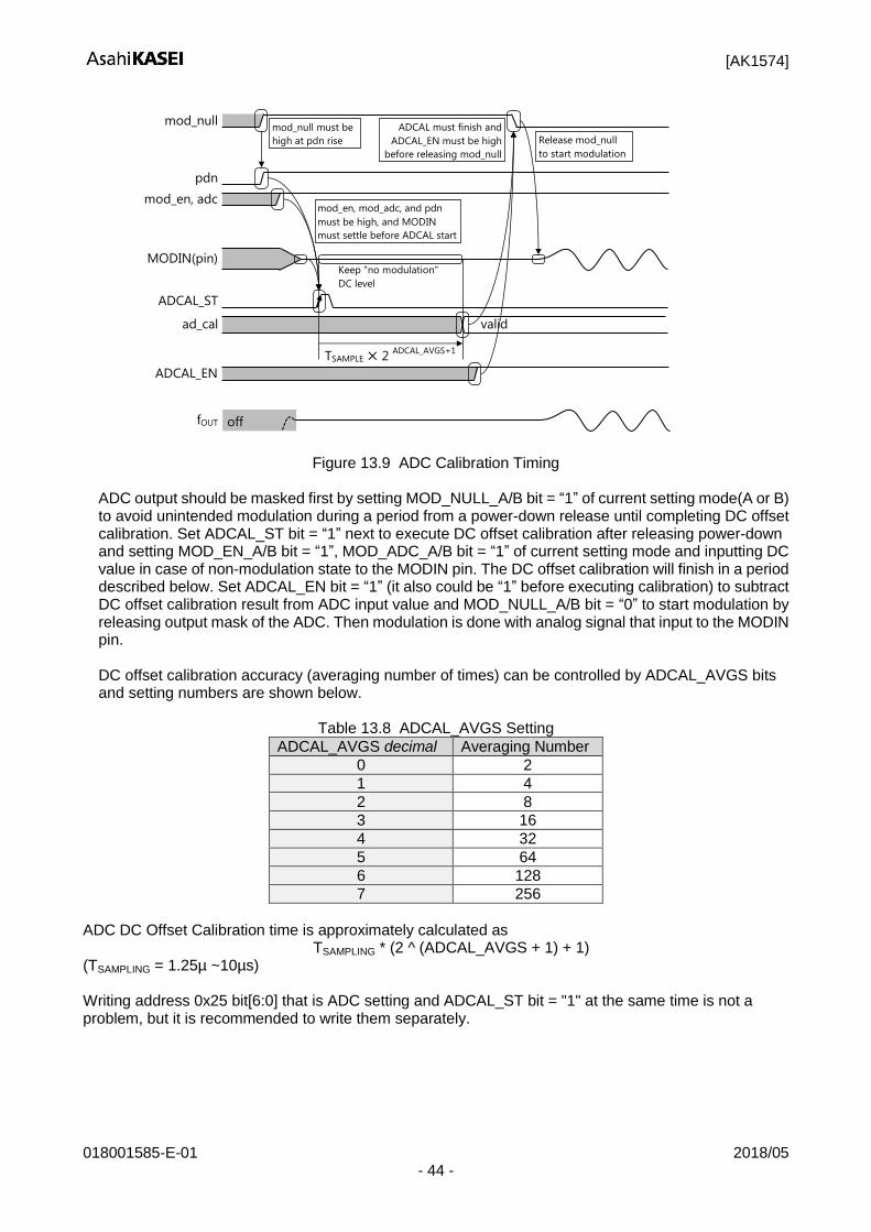
[AK1574]
018001585-E-01 2018/05 - 44 -
Figure 13.9 ADC Calibration Timing
ADC output should be masked first by setting MOD_NULL_A/B bit = “1” of current setting mode(A or B) to avoid unintended modulation during a period from a power-down release until completing DC offset calibration. Set ADCAL_ST bit = “1” next to execute DC offset calibration after releasing power-down and setting MOD_EN_A/B bit = “1”, MOD_ADC_A/B bit = “1” of current setting mode and inputting DC value in case of non-modulation state to the MODIN pin. The DC offset calibration will finish in a period described below. Set ADCAL_EN bit = “1” (it also could be “1” before executing calibration) to subtract DC offset calibration result from ADC input value and MOD_NULL_A/B bit = “0” to start modulation by releasing output mask of the ADC. Then modulation is done with analog signal that input to the MODIN pin. DC offset calibration accuracy (averaging number of times) can be controlled by ADCAL_AVGS bits and setting numbers are shown below.
Table 13.8 ADCAL_AVGS Setting
ADCAL_AVGS decimal Averaging Number
0 2
1 4
2 8
3 16
4 32
5 64
6 128
7 256
ADC DC Offset Calibration time is approximately calculated as
TSAMPLING * (2 ^ (ADCAL_AVGS + 1) + 1) (TSAMPLING = 1.25µ ~10µs) Writing address 0x25 bit[6:0] that is ADC setting and ADCAL_ST bit = "1" at the same time is not a problem, but it is recommended to write them separately.
mod_null
mod_en, adc
pdn
MODIN(pin)
ADCAL_ST
ad_cal valid
ADCAL_EN
mod_null must be
high at pdn rise
TSAMPLE × 2 ADCAL_AVGS+1
fOUT off
mod_en, mod_adc, and pdn
must be high, and MODIN
must settle before ADCAL start
ADCAL must finish and
ADCAL_EN must be high
before releasing mod_null Release mod_null
to start modulation
Keep "no modulation"
DC level
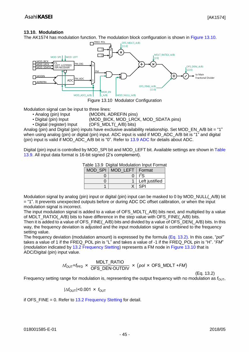
[AK1574]
018001585-E-01 2018/05 - 45 -
13.10. Modulation The AK1574 has modulation function. The modulation block configuration is shown in Figure 13.10.
Figure 13.10 Modulator Configuration
Modulation signal can be input to three lines: • Analog (pin) Input (MODIN, ADREFIN pins) • Digital (pin) Input (MOD_BICK, MOD_LRCK, MOD_SDATA pins) • Digital (register) Input (OFS_MDLT(_A/B) bits)
Analog (pin) and Digital (pin) inputs have exclusive availability relationship. Set MOD_EN_A/B bit = “1” when using analog (pin) or digital (pin) input. ADC input is valid if MOD_ADC_A/B bit is “1” and digital (pin) input is valid if MOD_ADC_A/B bit is “0”. Refer to 13.9 ADC for details about ADC. Digital (pin) input is controlled by MOD_SPI bit and MOD_LEFT bit. Available settings are shown in Table 13.9. All input data format is 16-bit signed (2’s complement).
Table 13.9 Digital Modulation Input Format
MOD_SPI MOD_LEFT Format
0 0 I2S
0 1 Left justified
1 X SPI
Modulation signal by analog (pin) input or digital (pin) input can be masked to 0 by MOD_NULL(_A/B) bit = “1”. It prevents unexpected outputs before or during ADC DC offset calibration, or when the input modulation signal is incorrect. The input modulation signal is added to a value of OFS_MDLT(_A/B) bits next, and multiplied by a value of MDLT_RATIO(_A/B) bits to have difference in the step value with OFS_FINE(_A/B) bits. Then it is added to a value of OFS_FINE(_A/B) bits and divided by a value of OFS_DEN(_A/B) bits. In this way, the frequency deviation is adjusted and the input modulation signal is combined to the frequency setting value. The frequency deviation (modulation amount) is expressed by the formula (Eq. 13.2). In this case, “pol” takes a value of 1 if the FREQ_POL pin is “L” and takes a value of -1 if the FREQ_POL pin is “H”. “FM” (modulation indicated by 13.2 Frequency Stetting) represents a FM node in Figure 13.10 that is ADC/Digital (pin) input value.
∆fOUT=fPFD × MDLT_RATIO
OFS_DEN∙OUTDIV × (pol × OFS_MDLT +FM)
(Eq. 13.2) Frequency setting range for modulation is, representing the output frequency with no modulation as fOUT,
|∆fOUT|<0.001 × fOUT
if OFS_FINE = 0. Refer to 13.2 Frequency Stetting for detail.
ADC
I2S/LEFT-JUSTIFIED/SPI RECEIVER
MODIN
ADREFIN
FM_ADC
FM_DIG
MOD_SDATA
MOD_LRCK
MOD_BICK
MOD_ADC(_A/B)
FM
FREQ_POL
1
-1 1
0
1
0
OFS_MDLT(_A/B)
[11:0]
MDLT_RATIO(_A/B)
[2:0]
OFS_DEN(_A/B)
[22:0]
OFS_FINE(_A/B)
[11:0]
MOD_NULL(_A/B)
MOD_EN
(_A/B)
to Main
Fractional Divider
MOD_SPI MOD_LEFT

[AK1574]
018001585-E-01 2018/05 - 46 -
Since OFS_DEN = 0x7FFFFF (8,388,607) is the maximum value, the minimum modulation step (Hz/LSB) will be
fPFD/(8388607*2) = 3.58Hz/LSB (at fPFD=60MHz) ~ 0.60Hz/LSB (at fPFD=10MHz) and the frequency deviation range is
Analog (pin) Input/ Digital (register) Input: 12 bits signed (-2048~+2047). ±7.32kHz (at fPFD=60MHz) ~ ±1.22kHz (at fPFD=10MHz)
Digital (pin) Input: 16 bits signed (-32768~+32767). ±min (117kHz, 0.001fOUT) (at fPFD=60MHz) ~ ±19.5kHz (at fPFD=10MHz)
When DSM_AT_INT bit = “0”, modulation signals and OFS_MDLT(_A/B), OFS_FINE(_A/B) bits should be 0 and the (Eq. 13.3) must be satisfied.
fOUT=fPFD × ( INT+
FRACMOD
OUTDIV)
(Eq. 13.3) When spurious occurs in the output signal, set OFS_FINE(_A/B) bit to avoid 0, negative odd number and positive even number. This eliminates the periodicity of internal operation, which may improve spurious. At this time, it is recommended to set the maximum value (all 1) for OFS_DEN(_A/B) bit.
13.11. REFDIVOUT Reference Frequency Divided Output The AK1574 is able to output reference frequency, that is input to the REFCKIN pin, in CMOS level after dividing by 1~4 from the REFDIVOUT pin. For example, it is capable of providing a 19.2MHz system clock of a DSP when using 57.6MHz reference frequency by dividing the reference signal by three. Dividing number can be set as “N+1” by setting REFOUTDIV bits assuming the setting value is “N”. Phase relationship between REFCKIN and REFDIVOUT can be controlled by REFDIVOUT_POL bit as shown in Figure 13.11.
Figure 13.11 REFOUTDIV and REFDIVOUT_POL Settings
REFDIVOUT output is fixed to zero data when REFDIVOUT_EN bit = “0” and becomes valid by writing “1” to REFDIVOUT_EN bit. REFDIVOUT can be output even in a power-down state by setting DIVOUT_AT_PDN bit = “1” so that an external DSP can be operated continuously during operation such as time-sharing. REFDIVOUT output is fixed to zero in power-down state when DIVOUT_AT_PDN bit setting is “0”. The output drivability becomes 4 times higher by setting REFDIVOUT_DS bit “1” for when output frequency is high or when heavy load is applied to the device.
REFCKIN
REFDIVOUT
REFOUTDIV=0
REFDIVOUT_POL=0
REFOUTDIV=0
REFDIVOUT_POL=1
REFOUTDIV=1
REFDIVOUT_POL=0
REFOUTDIV=1
REFDIVOUT_POL=1
REFOUTDIV=2
REFDIVOUT_POL=0
REFOUTDIV=2
REFDIVOUT_POL=1
REFOUTDIV=3
REFDIVOUT_POL=0
REFOUTDIV=3
REFDIVOUT_POL=1
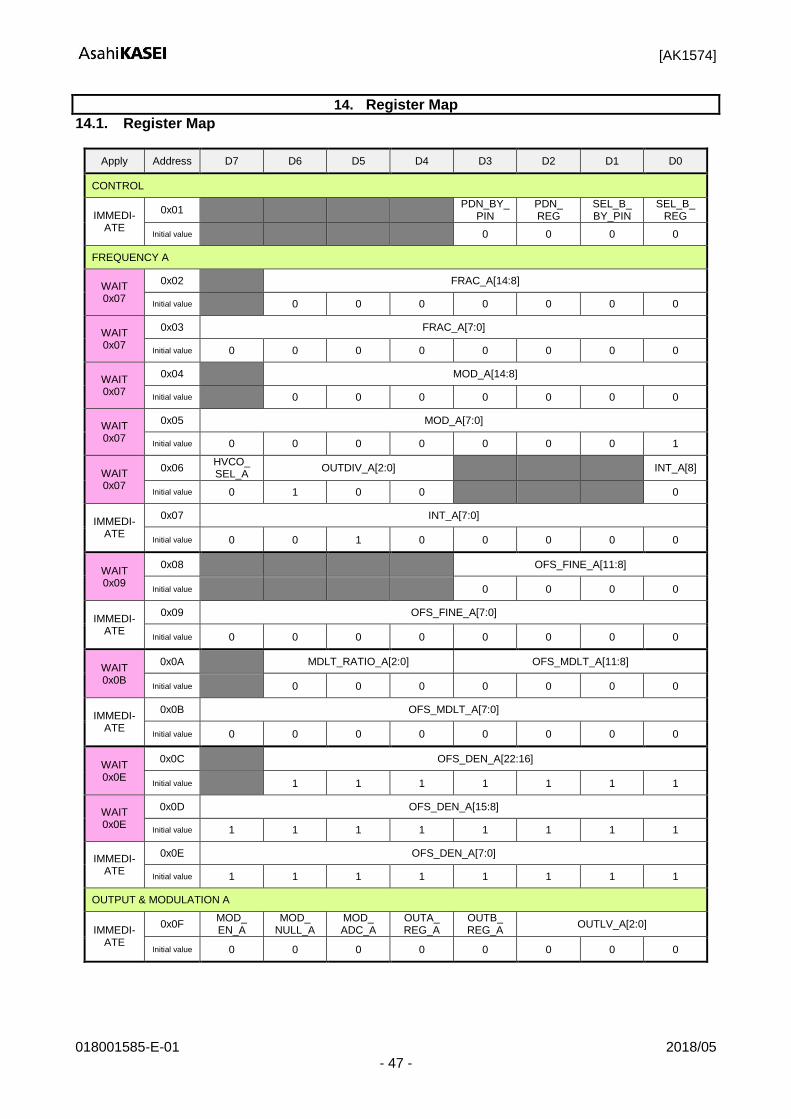
[AK1574]
018001585-E-01 2018/05 - 47 -
14. Register Map
14.1. Register Map
Apply Address D7 D6 D5 D4 D3 D2 D1 D0
CONTROL
IMMEDI- ATE
0x01 PDN_BY_
PIN PDN_ REG
SEL_B_ BY_PIN
SEL_B_ REG
Initial value 0 0 0 0
FREQUENCY A
WAIT 0x07
0x02 FRAC_A[14:8]
Initial value 0 0 0 0 0 0 0
WAIT 0x07
0x03 FRAC_A[7:0]
Initial value 0 0 0 0 0 0 0 0
WAIT 0x07
0x04 MOD_A[14:8]
Initial value 0 0 0 0 0 0 0
WAIT 0x07
0x05 MOD_A[7:0]
Initial value 0 0 0 0 0 0 0 1
WAIT 0x07
0x06 HVCO_ SEL_A
OUTDIV_A[2:0] INT_A[8]
Initial value 0 1 0 0 0
IMMEDI- ATE
0x07 INT_A[7:0]
Initial value 0 0 1 0 0 0 0 0
WAIT 0x09
0x08 OFS_FINE_A[11:8]
Initial value 0 0 0 0
IMMEDI- ATE
0x09 OFS_FINE_A[7:0]
Initial value 0 0 0 0 0 0 0 0
WAIT 0x0B
0x0A MDLT_RATIO_A[2:0] OFS_MDLT_A[11:8]
Initial value 0 0 0 0 0 0 0
IMMEDI- ATE
0x0B OFS_MDLT_A[7:0]
Initial value 0 0 0 0 0 0 0 0
WAIT 0x0E
0x0C OFS_DEN_A[22:16]
Initial value 1 1 1 1 1 1 1
WAIT 0x0E
0x0D OFS_DEN_A[15:8]
Initial value 1 1 1 1 1 1 1 1
IMMEDI- ATE
0x0E OFS_DEN_A[7:0]
Initial value 1 1 1 1 1 1 1 1
OUTPUT & MODULATION A
IMMEDI- ATE
0x0F MOD_ EN_A
MOD_ NULL_A
MOD_ ADC_A
OUTA_ REG_A
OUTB_ REG_A
OUTLV_A[2:0]
Initial value 0 0 0 0 0 0 0 0

[AK1574]
018001585-E-01 2018/05 - 48 -
Apply Address D7 D6 D5 D4 D3 D2 D1 D0
FREQUENCY B
WAIT 0x17
0x12 FRAC_B[14:8]
Initial value 0 0 0 0 0 0 0
WAIT 0x17
0x13 FRAC_B[7:0]
Initial value 0 0 0 0 0 0 0 0
WAIT 0x17
0x14 MOD_B[14:8]
Initial value 0 0 0 0 0 0 0
WAIT 0x17
0x15 MOD_B[7:0]
Initial value 0 0 0 0 0 0 0 1
WAIT 0x17
0x16 HVCO_ SEL_B
OUTDIV_B[2:0] INT_B[8]
Initial value 0 1 0 0 0
IMMEDI- ATE
0x17 INT_B[7:0]
Initial value 0 0 1 0 0 0 0 0
WAIT 0x19
0x18 OFS_FINE_B[11:8]
Initial value 0 0 0 0
IMMEDI- ATE
0x19 OFS_FINE_B[7:0]
Initial value 0 0 0 0 0 0 0 0
WAIT 0x1B
0x1A MDLT_RATIO_B[2:0] OFS_MDLT_B[11:8]
Initial value 0 0 0 0 0 0 0
IMMEDI- ATE
0x1B OFS_MDLT_B[7:0]
Initial value 0 0 0 0 0 0 0 0
WAIT 0x1E
0x1C OFS_DEN_B[22:16]
Initial value 1 1 1 1 1 1 1
WAIT 0x1E
0x1D OFS_DEN_B[15:8]
Initial value 1 1 1 1 1 1 1 1
IMMEDI- ATE
0x1E OFS_DEN_B[7:0]
Initial value 1 1 1 1 1 1 1 1
OUTPUT & MODULATION B
IMMEDI- ATE
0x1F MOD_ EN_B
MOD_ NULL_B
MOD_ ADC_B
OUTA_ REG_B
OUTB_ REG_B
OUTLV_B[2:0]
Initial value 0 0 0 0 0 0 0 0

[AK1574]
018001585-E-01 2018/05 - 49 -
Apply Address D7 D6 D5 D4 D3 D2 D1 D0
REFDIVOUT
IMMEDI- ATE
0x20 DIVOUT_ AT_PDN
REFDIVOUT_EN
REFDIVOUT_DS
REFDIVOUT_POL
REFOUTDIV[1:0]
Initial value 0 0 0 0 0 0
CP
IMMEDI- ATE
0x21 CPSRC_I[2:0] ICP_FAST[1:0] ICP_NORM[1:0]
Initial value 0 0 0 1 1 0 0
IMMEDI- ATE
0x22 LD_SEL[1:0] FAST_EN FAST_TIME[3:0]
Initial value 0 0 1 0 0 0 1
VCO
IMMEDI- ATE
0x23 LD_TIME MUTE_ UNLKD
DSM_ AT_INT
VCOI VCOCAL_TIME[3:0]
Initial value 0 1 0 0 1 0 1 1
MODULATION I/F
IMMEDI- ATE
0x24 TEST_1 MOD_SPI MOD_ LEFT
Initial value 0 0 0
ADC
IMMEDI- ATE
0x25 ADCAL_
ST AD_CKDIV[1:0]
AD_EXT_ REF
ADCAL_ EN
ADCAL_AVGS[2:0]
Initial value 0 0 0 0 0 1 1 1
FREQUENCY A
WAIT 0x07
0x26 MULT_A[5:0]
Initial value 0 0 0 0 0 1
WAIT 0x07
0x27 R_A[5:0]
Initial value 0 0 0 0 0 1
FREQUENCY B
WAIT 0x17
0x28 MULT_B[5:0]
Initial value 0 0 0 0 0 1
WAIT 0x17
0x29 R_B[5:0]
Initial value 0 0 0 0 0 1
General Purpose Registers
IMMEDI- ATE
0x2A MASK_
DIG_CLK GPREG[6:0]
Initial value 0 0 0 0 0 0 0 0
RESET
IMMEDI- ATE
0x2B Write "0100 1010" to trigger Software Reset
Initial value
Name Processing starts when writing
Initial value The value changes after processing
[AK1574]
018001585-E-01 2018/05 - 50 -
14.2. Special Register Access
Following registers have restriction in writing order stem from internal buffer.
Address 0x02 ~ 0x07, 0x26, 0x27: Frequency Setting A When writing to address 0x02~0x07, 0x26, 0x27, all registers must be written. (If registers are partly written, register values will be over written by default value of the buffer) Register write must be executed in the order of address 0x26->0x27->0x02 -> 0x03 -> 0x04 -> 0x05 -> 0x06-> 0x07. (It is prohibited to write to a register other than address 0x27, 0x02 ~ 0x06 during this register write sequence from 0x26 to 0x07. If not, the buffer data will be deleted) Written register values are valid when the address 0x07 is written.
Address 0x08, 0x09: OFS_FINE_A
When writing to address 0x08 and 0x09, both registers must be written. (If registers are partly written, register values will be over written by default value of the buffer) Register write must be executed sequentially in the order of address 0x08 -> 0x09. (It is prohibited to write to a register other than address 0x08 and 0x09 during this register write sequence. If not, the buffer data will be deleted) Written register values are valid when the address 0x09 is written. When there is spurious in the output signal, set OFS_FINE(_A/B) bit to “0”, a negative odd number or a positive even number. This eliminates the periodicity of internal operation, and may improve spurious. At this time, it is recommended to set the maximum value (all 1) for OFS_DEN(_A/B).
Address 0x0A, 0x0B: MDLT_RATIO_A, OFS_MDLT_A
When writing to address 0x0A and 0x0B, both registers must be written. (If registers are partly written, register values will be over written by default value of the buffer) Register write must be executed sequentially in the order of address 0x0A -> 0x0B. (It is prohibited to write to a register other than address 0x0A and 0x0B during this register write sequence. If not, the buffer data will be deleted) Written register values are valid when the address 0x0B is written.
Address 0x0C, 0x0D, 0x0E: OFS_DEN_A
When writing to address 0x0C, 0x0D and 0x0E, all registers must be written. (If registers are partly written, register values will be over written by default value of the buffer) Register write must be executed sequentially in the order of address 0x0C -> 0x0D -> 0x0E. (It is prohibited to write to a register other than address 0x0C ~ 0x0E during this register write sequence. If not, the buffer data will be deleted) Written register values are valid when the address 0x0E is written.
Address 0x12 ~ 0x17, 0x28, 0x29: Frequency Setting B
When writing to address 0x12 ~ 0x17, 0x28, 0x29, all registers must be written. (If registers are partly written, register values will be over written by default value of the buffer) Register write must be executed sequentially in the order of address 0x28 -> 0x29 -> 0x12 -> 0x13 -> 0x14 -> 0x15 -> 0x16 -> 0x17. (It is prohibited to write to a register other than address 0x29, 0x12 ~ 0x16 during this register write sequence from 0x28 to 0x17. If not, the buffer data will be deleted) Written register values are valid when the address 0x17 is written.
[AK1574]
018001585-E-01 2018/05 - 51 -
Address 0x18, 0x19: OFS_FINE_B When writing to address 0x18 and 0x19, both registers must be written. (If registers are partly written, register values will be over written by default value of the buffer) Register write must be executed sequentially in the order of address 0x18 -> 0x19. (It is prohibited to write to a register other than address 0x18 and 0x19 during this register write sequence. If not, the buffer data will be deleted) Written register values are valid when the address 0x19 is written. When there is spurious in the output signal, set OFS_FINE_A/B bit to “0”, a negative odd number or a positive even number. This eliminates the periodicity of internal operation, and may improve spurious. At this time, it is recommended to set the maximum value (all 1) for OFS_DEN_A/B.
Address 0x1A, 0x1B: MDLT_RATIO_B, OFS_MDLT_B When writing to address 0x1A and 0x1B, both registers must be written. (If registers are partly written, register values will be over written by default value of the buffer) Register write must be executed sequentially in the order of address 0x1A -> 0x1B. (It is prohibited to write to a register other than address 0x1A and 0x1B during this register write sequence. If not, the buffer data will be deleted) Written register values are valid when the address 0x1B is written.
Address 0x1C, 0x1D, 0x1E: OFS_DEN_B
When writing to address 0x1C, 0x1D and 0x1E, all registers must be written. (If registers are partly written, register values will be over written by default value of the buffer) Register write must be executed sequentially in the order of address 0x1C -> 0x1D -> 0x1E. (It is prohibited to write to a register other than address 0x1C ~ 0x1E during this register write sequence. If not, the buffer data will be deleted) Written register values are valid when the address 0x1E is written.
Registers below have different restrictions.
Address 0x24 bit[7] : TEST_1
This bit is a test bit. Write “0” to this bit.
Address 0x25 bit[7]: ADCAL_ST When writing “1” to ADCAL_ST bit, asynchronous synchronization of DIVCLK at the phase frequency detector (PFD) is executed. Writing address 0x25 bit[6:0] that is ADC setting and ADCAL_ST bit = "1" at the same time is not a problem, but it is recommended to write them separately.
Address 0x2B bit[7:0]: SW_RST
Software reset is executed when writing SW_RST bit = “0100 1010” to this register.
14.3. Register Definitions Address 0x01
bit[3] PDN_BY_PIN bit[2] PDN_REG
Power-down is executed in a logic shown in Table 14.1. Table 14.1 PDN Logic
PDN_BY_PIN bit PDN_REG bit PDN pin State
0 0 X Power Down Mode
0 1 X Active
1 X L Power Down Mode
1 X H Active
bit[1] SEL_B_BY_PIN bit[0] SEL_B_REG
Mode A/B is selected in a logic shown in Table 14.2.
[AK1574]
018001585-E-01 2018/05 - 52 -
Table 14.2 Mode A/B Select Logic
SEL_B_BY_PIN bit SEL_B_REG bit SEL_B pin Mode
0 0 X A
0 1 X B
1 X L A
1 X H B
Address 0x02 ~ 0x0F, 0x26, 0x27: mode A
Frequency, Modulation and Output Settings of Mode A
Address 0x12 ~ 0x1F, 0x28, 0x29: mode B Frequency, Modulation and Output Settings of Mode B As mentioned in 14.2 Special Register Access, registers below have restrictions in writing order (Table 14.3).
Table 14.3 Register Write Restrictions
Address Function Constraint Updated when
0x02~0x07 0x26~0x27
Frequency Setting A Must write all these registers in the order of: 0x26->0x27->0x02->0x03->0x04 ->0x05->0x06>0x07
address 0x07 is written
0x08~0x09 OFS_FINE A Must write all these registers in the order of: 0x08->0x09
address 0x09 is written
0x0A~0x0B MDLT_RATIO A OFS_MDLT A
Must write all these registers in the order of: 0x0A->0x0B
address 0x0B is written
0x0C~0x0E OFS_DEN A Must write all these registers in the order of: 0x0C->0x0D->0x0E
address 0x0E is written
0x12~0x17 0x28~0x29
Frequency Setting B Must write all these registers in the order of: 0x28->0x29->0x12->0x13->0x14 ->0x15->0x16->0x17
address 0x17 is written
0x18~0x19 OFS_FINE B Must write all these registers in the order of: 0x18->0x19
address 0x19 is written
0x1A~0x1B MDLT_RATIO_B OFS_MDLT B
Must write all these registers in the order of: 0x1A->0x1B
address 0x1B is written
0x1C~0x1E OFS_DEN B Must write all these registers in the order of: 0x1C->0x1D->0x1E
address 0x1E is written
The output frequency setting is already mentioned in13.2 Frequency Stetting. Here, the calculation formula of output frequency is shown below.
fOUT=fPFD
OUTDIV × (INT+
FRAC
MOD+
MDLT_RATIO × (pol × OFS_MDLT+modulation)+OFS_FINE
OFS_DEN)
(Eq. 14.1)
In this formula, OUTDIV and MDLT_RATIO take decoded values from OUTDIV bits and MDLT_RATIO bits (e.g. OUTDIV bit=“11” -> 8), “pol” takes a value according to the FREQ_POL pin (It will be “1” when FREQ_POL pin = “L”, and “-1” when FREQ_POL pin = “H”) and “modulation” takes a digital input value for modulation or an A/D converted analog input value.
[AK1574]
018001585-E-01 2018/05 - 53 -
address 0x02 bit[6:0], address 0x03 bit[7:0] FRAC_A address 0x12 bit[6:0], address 0x13 bit[7:0] FRAC_B
N COUNTER Fraction Division Numerator Setting “0 ≤ FRAC < MOD” should be satisfied. (unsigned) When zero is set to FRAC(_A/B), the delta-sigma block stops operation if DSM_AT_INT bit=“0”, and works as integer-N PLL.
address 0x04 bit[6:0], address 0x05 bit[7:0] MOD_A address 0x14 bit[6:0], address 0x15 bit[7:0] MOD_B
N COUNTER Fraction Division Denominator Setting “2 ≤ MOD ≤ 32767” should be satisfied.
address 0x06 bit[7] HVCO_SEL_A address 0x16 bit[7] HVCO_SEL_B
Select VCO oscillation range. 0: 1500 ~ 2100 MHz (LVCO) 1: 2100 ~ 3365 MHz (HVCO)
address 0x06 bit[6:4] OUTDIV_A address 0x16 bit[6:4] OUTDIV_B
RFOUT Output Dividing Number Setting Setting values are shown in Table 14.4.
Table 14.4 RFOUT Output Dividing Number Setting
OUTDIV_A/B decimal
Divider Ratio
0 prohibited
1 2
2 4
3 8
4 16
5 32
6 prohibited
7 prohibited
address 0x06 bit[0], address 0x07 bit[7:0] INT_A address 0x16 bit[0], address 0x17 bit[7:0] INT_B
N COUNTER Integer Dividing Number Setting VCO frequency should be in the range of 1500 ~ 3365MHz. It is prohibited to set it to 27 or less. Therefore there is a VCO frequency that cannot be set when fPFD=(1500MHz/28)=53.57 MHz or higher.
address 0x08 bit[3:0], address 0x09 bit[7:0] OFS_FINE_A address 0x18 bit[3:0], address 0x19 bit[7:0] OFS_FINE_B
Set an offset value for most small steps. Available setting range is -2048 (0x800) ~ +2047 (0x7FF) when data is signed. These registers are to compensate frequency shift of TCXO. When spurious occurs in the output signal, set it to avoid 0, negative odd number and positive even number. This eliminates the periodicity of internal operation, which may improve spurious. At this time, it is recommended to set the maximum value (all 1) for OFS_DEN.
address 0x0A bit[6:4], MDLT_RATIO_A address 0x1A bit[6:4], MDLT_RATIO_B
Set a ratio between OFS_FINE and modulation signal. Settings are shown in Table 14.5.

[AK1574]
018001585-E-01 2018/05 - 54 -
Table 14.5 OFS_FINE, Modulation Step Ratio Setting
MDLT_RATIO_A/B decimal
Step Ratio
0 1
1 2
2 4
3 8
4 16
5 prohibited
6 prohibited
7 prohibited
address 0x0A bit[3:0], address 0x0B bit[7:0] OFS_MDLT_A address 0x1A bit[3:0], address 0x1B bit[7:0] OFS_MDLT_B
Offset value is set by multiplying step value by MDLT_RATIO. The data format is signed and setting range is from -2048 (0x800) to +2047 (0x7FF). It is used for fine adjustment of frequency and modulation.
address 0x0C bit[6:0], address 0x0D bit[7:0], address 0x0E bit[7:0] OFS_DEN_A address 0x1C bit[6:0], address 0x1D bit[7:0], address 0x1E bit[7:0] OFS_DEN_B
Set denominator of modulation for OFS_FINE(_A/B) and OFS_MDLT(_A/B). The data format is unsigned, and setting value should be larger than 1 and satisfy the (Eq. 14.2).
|MDLT_RATIO × (pol × OFS_MDLT+modulation)
OFS_DEN| <0.001 × (INT+
FRAC
MOD+
OFS_FINE
OFS_DEN)
(Eq. 14.2) (VCO Modulation < ±0.1%)
address 0x26 bit[5:0], MULT_A address 0x28 bit[5:0], MULT_B
Reference clock multiplier number (unsigned) Due to frequency constraints of fREF and fPFD, MULT=1 or 6~50(dec)
address 0x27 bit[5:0], R_A address 0x29 bit[5:0], R_B
Reference clock dividing number (unsigned) Due to frequency constraints of fREF and fPFD, R=1~50(dec) R COUNTER can be used only when the multiplier is used (MULT≠1). It is prohibited to set it to anything other than R=1 when the multiplier is not used (MULT=1)
address 0x0F bit[7], MOD_EN_A address 0x1F bit[7] ,MOD_EN_B ADC or Digital interface for modulation enable
0: Disable 1: Enable (ADC or Digital I/F is selected by MOD_ADC(_A/B) bits)
address 0x0F bit[6] MOD_NULL_A address 0x1F bit[6] MOD_NULL_B Mask modulation signal to 0. It is used when a correct value is not input after I/F or ADC power-down is released or to prevent unexpected signal during ADC DC offset calibration.
0: Execute Modulation (using modulation signal) 1: Do Not Execute Modulation (mask modulation signal that is input to ADC or digital I/F to 0)
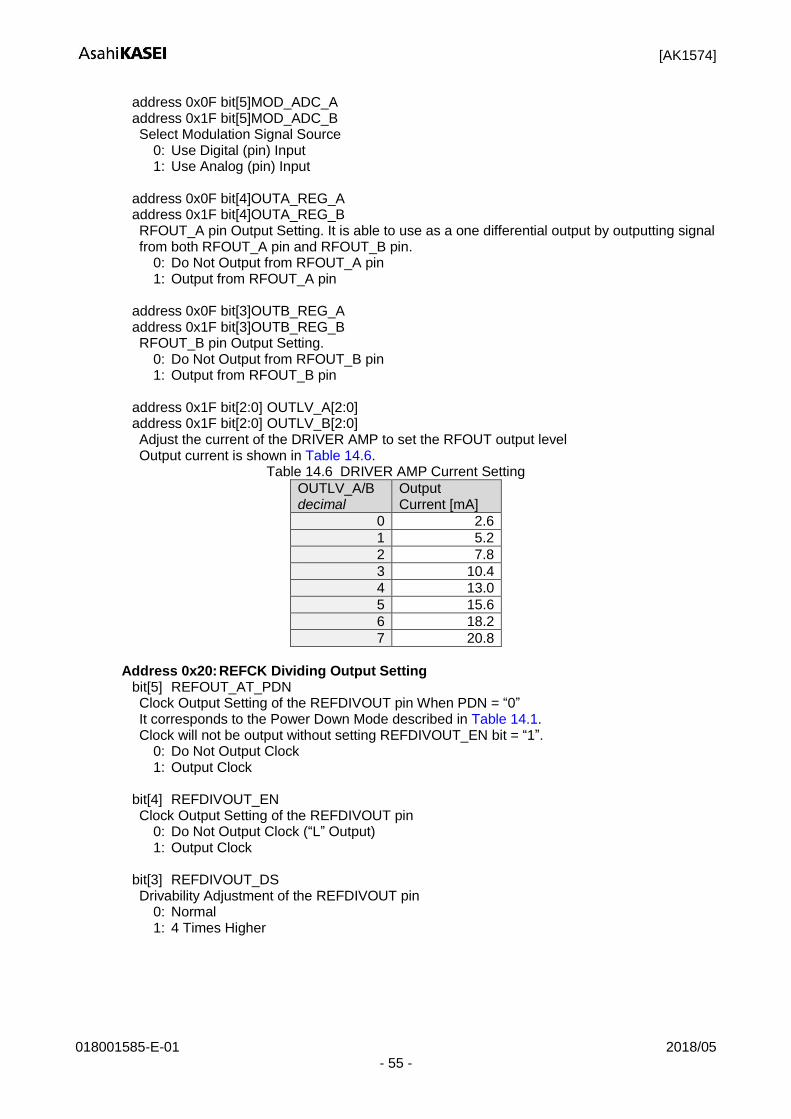
[AK1574]
018001585-E-01 2018/05 - 55 -
address 0x0F bit[5] MOD_ADC_A address 0x1F bit[5] MOD_ADC_B Select Modulation Signal Source
0: Use Digital (pin) Input 1: Use Analog (pin) Input
address 0x0F bit[4] OUTA_REG_A address 0x1F bit[4] OUTA_REG_B RFOUT_A pin Output Setting. It is able to use as a one differential output by outputting signal from both RFOUT_A pin and RFOUT_B pin.
0: Do Not Output from RFOUT_A pin 1: Output from RFOUT_A pin
address 0x0F bit[3] OUTB_REG_A address 0x1F bit[3] OUTB_REG_B RFOUT_B pin Output Setting.
0: Do Not Output from RFOUT_B pin 1: Output from RFOUT_B pin
address 0x1F bit[2:0] OUTLV_A[2:0] address 0x1F bit[2:0] OUTLV_B[2:0] Adjust the current of the DRIVER AMP to set the RFOUT output level Output current is shown in Table 14.6.
Table 14.6 DRIVER AMP Current Setting
OUTLV_A/B decimal
Output Current [mA]
0 2.6
1 5.2
2 7.8
3 10.4
4 13.0
5 15.6
6 18.2
7 20.8
Address 0x20: REFCK Dividing Output Setting
bit[5] REFOUT_AT_PDN Clock Output Setting of the REFDIVOUT pin When PDN = “0” It corresponds to the Power Down Mode described in Table 14.1. Clock will not be output without setting REFDIVOUT_EN bit = “1”.
0: Do Not Output Clock 1: Output Clock
bit[4] REFDIVOUT_EN Clock Output Setting of the REFDIVOUT pin
0: Do Not Output Clock (“L” Output) 1: Output Clock
bit[3] REFDIVOUT_DS Drivability Adjustment of the REFDIVOUT pin
0: Normal 1: 4 Times Higher
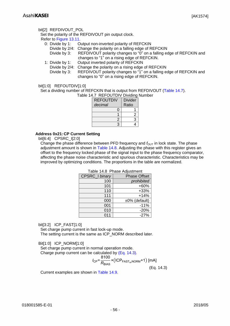
[AK1574]
018001585-E-01 2018/05 - 56 -
bit[2] REFDIVOUT_POL Set the polarity of the REFDIVOUT pin output clock. Refer to Figure 13.11.
0: Divide by 1: Output non-inverted polarity of REFCKIN Divide by 2/4: Change the polarity on a falling edge of REFCKIN
Divide by 3: REFDIVOUT polarity changes to “0” on a falling edge of REFCKIN and changes to “1” on a rising edge of REFCKIN.
1: Divide by 1: Output inverted polarity of REFCKIN Divide by 2/4: Change the polarity on a rising edge of REFCKIN
Divide by 3: REFDIVOUT polarity changes to “1” on a falling edge of REFCKIN and changes to “0” on a rising edge of REFCKIN.
bit[1:0] REFOUTDIV[1:0] Set a dividing number of REFCKIN that is output from REFDIVOUT (Table 14.7).
Table 14.7 REFOUTDIV Dividing Number
REFOUTDIV decimal
Divider Ratio
0 1
1 2
2 3
3 4
Address 0x21: CP Current Setting
bit[6:4] CPSRC_I[2:0] Change the phase difference between PFD frequency and fOUT in lock state. The phase adjustment amount is shown in Table 14.8. Adjusting the phase with this register gives an offset to the frequency locked phase of the signal input to the phase frequency comparator, affecting the phase noise characteristic and spurious characteristic. Characteristics may be improved by optimizing conditions. The proportions in the table are normalized.
Table 14.8 Phase Adjustment
CPSRC_I binary Phase Offset
100 prohibited
101 +60%
110 +33%
111 +14%
000 ±0% (default)
001 -11%
010 -20%
011 -27%
bit[3:2] ICP_FAST[1:0] Set charge pump current in fast lock-up mode. The setting current is the same as ICP_NORM described later.
Bit[1:0] ICP_NORM[1:0] Set charge pump current in normal operation mode. Charge pump current can be calculated by (Eq. 14.3).
ICP=8100
RBIAS
×(ICPFASTorNORM+1) [mA]
(Eq. 14.3) Current examples are shown in Table 14.9.

[AK1574]
018001585-E-01 2018/05 - 57 -
Table 14.9 CP Current Examples
ICP_FAST/NORM decimal
CP current for 27kΩ [µA]
0 300
1 600
2 900
3 1200
Address 0x22: FAST Lock-up Settings
bit[7:6] LD_SEL[1:0] When locking to set frequency, "H" is output form LD pin. LD_SEL bits="1" or "2" are in test mode, setting prohibited. With "1" and "2" prohibited setting, there is a possibility of outputting "H" even in Unlock.
Table 14.10 LD pin Output Mode
LD_SEL
Decimal
0 Normal Operation
1 Prohibited
2 Prohibited
3 “H” fixed
bit[4] FAST_EN Fast Lock-up Mode Enable/Disable
0: Fast Lock-up Mode Disable 1: Fast Lock-up Mode Enable
bit[3:0] FAST_TIME[3:0] Set the valid time of fast lock-up mode.
Valid time = TPFD×(1023 + 1024 × FAST_TIME[3:0])
Table 14.11 shows setting examples.
Table 14.11 Fast Lock-up Mode Valid Time Setting
FAST_TIME decimal
Duration [µs] at 60MHz PFD
Duration [µs] at 10MHz PFD
0 17 102
1 34 205
2 51 307
3 68 410
4 85 512
5 102 614
6 119 717
7 137 819
8 154 922
9 171 1024
10 188 1126
11 205 1229
12 222 1331
13 239 1434
14 256 1536
15 273 1638
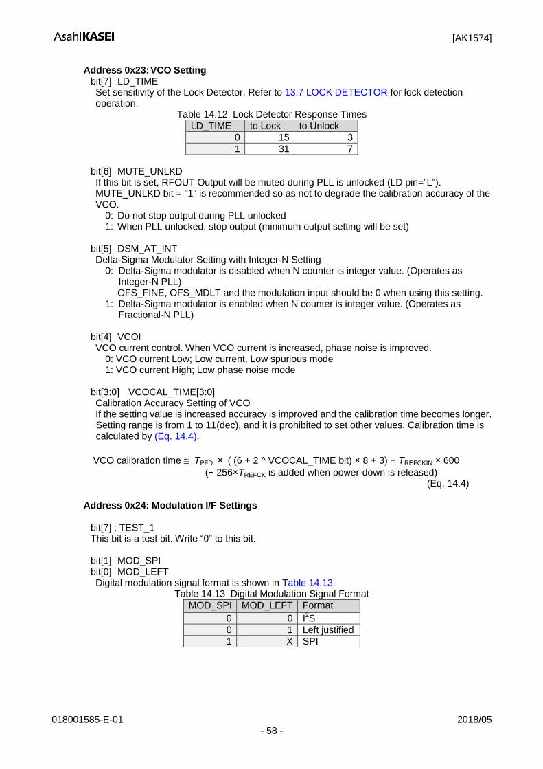
[AK1574]
018001585-E-01 2018/05 - 58 -
Address 0x23: VCO Setting bit[7] LD_TIME Set sensitivity of the Lock Detector. Refer to 13.7 LOCK DETECTOR for lock detection operation.
Table 14.12 Lock Detector Response Times
LD_TIME to Lock to Unlock
0 15 3
1 31 7
bit[6] MUTE_UNLKD If this bit is set, RFOUT Output will be muted during PLL is unlocked (LD pin=”L”). MUTE_UNLKD bit = "1" is recommended so as not to degrade the calibration accuracy of the VCO.
0: Do not stop output during PLL unlocked 1: When PLL unlocked, stop output (minimum output setting will be set)
bit[5] DSM_AT_INT Delta-Sigma Modulator Setting with Integer-N Setting
0: Delta-Sigma modulator is disabled when N counter is integer value. (Operates as Integer-N PLL)
OFS_FINE, OFS_MDLT and the modulation input should be 0 when using this setting. 1: Delta-Sigma modulator is enabled when N counter is integer value. (Operates as
Fractional-N PLL) bit[4] VCOI VCO current control. When VCO current is increased, phase noise is improved.
0: VCO current Low; Low current, Low spurious mode 1: VCO current High; Low phase noise mode
bit[3:0] VCOCAL_TIME[3:0] Calibration Accuracy Setting of VCO If the setting value is increased accuracy is improved and the calibration time becomes longer. Setting range is from 1 to 11(dec), and it is prohibited to set other values. Calibration time is calculated by (Eq. 14.4).
VCO calibration time TPFD × ( (6 + 2 ^ VCOCAL_TIME bit) × 8 + 3) + TREFCKIN × 600
(+ 256×TREFCK is added when power-down is released) (Eq. 14.4)
Address 0x24: Modulation I/F Settings
bit[7] : TEST_1 This bit is a test bit. Write “0” to this bit. bit[1] MOD_SPI bit[0] MOD_LEFT Digital modulation signal format is shown in Table 14.13.
Table 14.13 Digital Modulation Signal Format
MOD_SPI MOD_LEFT Format
0 0 I2S
0 1 Left justified
1 X SPI
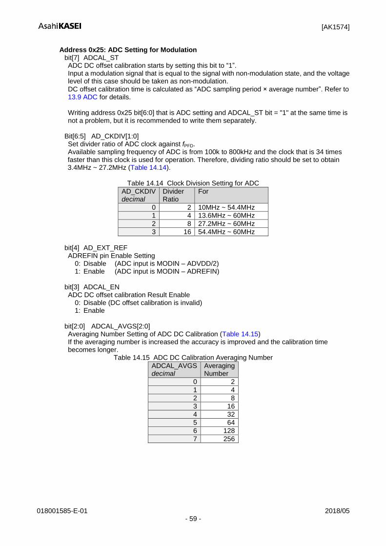
[AK1574]
018001585-E-01 2018/05 - 59 -
Address 0x25: ADC Setting for Modulation bit[7] ADCAL_ST ADC DC offset calibration starts by setting this bit to “1”. Input a modulation signal that is equal to the signal with non-modulation state, and the voltage level of this case should be taken as non-modulation. DC offset calibration time is calculated as “ADC sampling period × average number”. Refer to 13.9 ADC for details. Writing address 0x25 bit[6:0] that is ADC setting and ADCAL_ST bit = "1" at the same time is not a problem, but it is recommended to write them separately.
Bit[6:5] AD_CKDIV[1:0] Set divider ratio of ADC clock against fPFD. Available sampling frequency of ADC is from 100k to 800kHz and the clock that is 34 times faster than this clock is used for operation. Therefore, dividing ratio should be set to obtain 3.4MHz ~ 27.2MHz (Table 14.14).
Table 14.14 Clock Division Setting for ADC
AD_CKDIV decimal
Divider Ratio
For
0 2 10MHz ~ 54.4MHz
1 4 13.6MHz ~ 60MHz
2 8 27.2MHz ~ 60MHz
3 16 54.4MHz ~ 60MHz
bit[4] AD_EXT_REF ADREFIN pin Enable Setting
0: Disable (ADC input is MODIN – ADVDD/2) 1: Enable (ADC input is MODIN – ADREFIN)
bit[3] ADCAL_EN ADC DC offset calibration Result Enable
0: Disable (DC offset calibration is invalid) 1: Enable
bit[2:0] ADCAL_AVGS[2:0] Averaging Number Setting of ADC DC Calibration (Table 14.15) If the averaging number is increased the accuracy is improved and the calibration time becomes longer.
Table 14.15 ADC DC Calibration Averaging Number
ADCAL_AVGS decimal
Averaging Number
0 2
1 4
2 8
3 16
4 32
5 64
6 128
7 256

[AK1574]
018001585-E-01 2018/05 - 60 -
Address 0x2A: GPREG bit[7] MASK_DIG_CLK
Sets whether to stop CLK for digital circuits operating at REFCKIN frequency. Spurious characteristics may be affected by using this register 0: Do not stop the digital clock 1: Stop the digital clock VCO calibration cannot be performed while CLK is stopped. Therefore, refer to Figure 14.1
for the setting timing of the MASK_DIG_CLK bit. Refer to 13.5 VCO for VCO calibration.
Figure 14.1 Timing of MASK_DIG_CLK bit setting
It is possible to stop CLK by setting MASK_DIG_CLK bit="1" after waiting of 0.1ms or more
from the start of the VCO calibration. When VCO calibration is carried out again after stopping CLK, set MASK_DIG_CLK bit = "0"
and perform VCO calibration. At this time, no special standby time is necessary. The REFDIVOUT reference frequency divided output function will continue to operate even
when CLK is stopped by setting MASK_DIG_CLK bit = "1".
bit[6:0] GPREG[6:0] There is 7bits reserved register. No function is implemented to this register.
Address 0x2B: Software reset
Software reset is executed when writing "0100 1010" to this address. It works as the same as hardware reset.
VCO Calib. (Fast) Lockup LockUnlock
VCO Calibration startsVCO Calibrationstarts Flag
PLL/VCO state
LD pin
MASK_DIG_CLK bit
≧0.1ms
Lock
Do not care
MASK_DIG_CLK bit can be asserted (to "1")
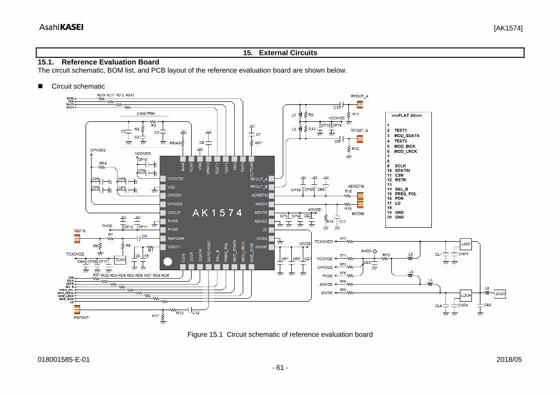
[AK1574]
018001585-E-01 2018/05 - 61 -
15. External Circuits
15.1. Reference Evaluation Board The circuit schematic, BOM list, and PCB layout of the reference evaluation board are shown below. Circuit schematic
Figure 15.1 Circuit schematic of reference evaluation board
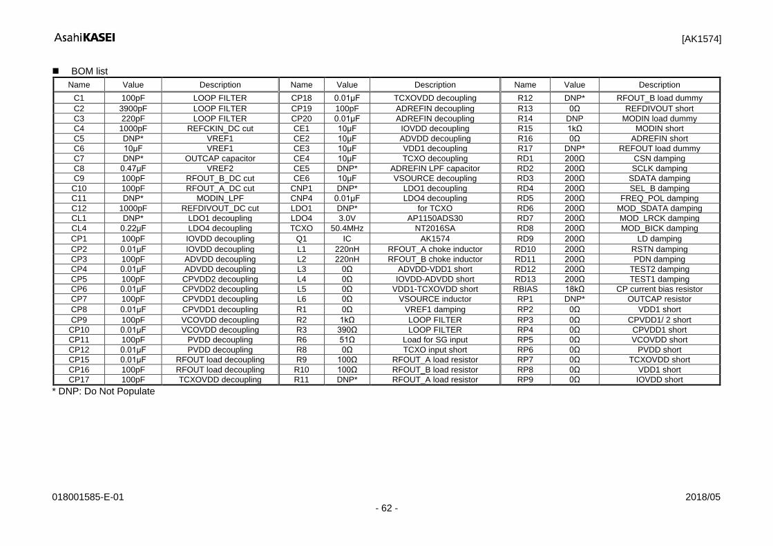
[AK1574]
018001585-E-01 2018/05 - 62 -
BOM list
Name Value Description Name Value Description Name Value Description
C1 100pF LOOP FILTER CP18 0.01μF TCXOVDD decoupling R12 DNP* RFOUT_B load dummy
C2 3900pF LOOP FILTER CP19 100pF ADREFIN decoupling R13 0Ω REFDIVOUT short
C3 220pF LOOP FILTER CP20 0.01μF ADREFIN decoupling R14 DNP MODIN load dummy
C4 1000pF REFCKIN_DC cut CE1 10μF IOVDD decoupling R15 1kΩ MODIN short
C5 DNP* VREF1 CE2 10μF ADVDD decoupling R16 0Ω ADREFIN short
C6 10μF VREF1 CE3 10μF VDD1 decoupling R17 DNP* REFOUT load dummy
C7 DNP* OUTCAP capacitor CE4 10μF TCXO decoupling RD1 200Ω CSN damping
C8 0.47μF VREF2 CE5 DNP* ADREFIN LPF capacitor RD2 200Ω SCLK damping
C9 100pF RFOUT_B_DC cut CE6 10μF VSOURCE decoupling RD3 200Ω SDATA damping
C10 100pF RFOUT_A_DC cut CNP1 DNP* LDO1 decoupling RD4 200Ω SEL_B damping
C11 DNP* MODIN_LPF CNP4 0.01μF LDO4 decoupling RD5 200Ω FREQ_POL damping
C12 1000pF REFDIVOUT_DC cut LDO1 DNP* for TCXO RD6 200Ω MOD_SDATA damping
CL1 DNP* LDO1 decoupling LDO4 3.0V AP1150ADS30 RD7 200Ω MOD_LRCK damping
CL4 0.22μF LDO4 decoupling TCXO 50.4MHz NT2016SA RD8 200Ω MOD_BICK damping
CP1 100pF IOVDD decoupling Q1 IC AK1574 RD9 200Ω LD damping
CP2 0.01μF IOVDD decoupling L1 220nH RFOUT_A choke inductor RD10 200Ω RSTN damping
CP3 100pF ADVDD decoupling L2 220nH RFOUT_B choke inductor RD11 200Ω PDN damping
CP4 0.01μF ADVDD decoupling L3 0Ω ADVDD-VDD1 short RD12 200Ω TEST2 damping
CP5 100pF CPVDD2 decoupling L4 0Ω IOVDD-ADVDD short RD13 200Ω TEST1 damping
CP6 0.01μF CPVDD2 decoupling L5 0Ω VDD1-TCXOVDD short RBIAS 18kΩ CP current bias resistor
CP7 100pF CPVDD1 decoupling L6 0Ω VSOURCE inductor RP1 DNP* OUTCAP resistor
CP8 0.01μF CPVDD1 decoupling R1 0Ω VREF1 damping RP2 0Ω VDD1 short
CP9 100pF VCOVDD decoupling R2 1kΩ LOOP FILTER RP3 0Ω CPVDD1/ 2 short
CP10 0.01μF VCOVDD decoupling R3 390Ω LOOP FILTER RP4 0Ω CPVDD1 short
CP11 100pF PVDD decoupling R6 51Ω Load for SG input RP5 0Ω VCOVDD short
CP12 0.01μF PVDD decoupling R8 0Ω TCXO input short RP6 0Ω PVDD short
CP15 0.01μF RFOUT load decoupling R9 100Ω RFOUT_A load resistor RP7 0Ω TCXOVDD short
CP16 100pF RFOUT load decoupling R10 100Ω RFOUT_B load resistor RP8 0Ω VDD1 short
CP17 100pF TCXOVDD decoupling R11 DNP* RFOUT_A load resistor RP9 0Ω IOVDD short
* DNP: Do Not Populate

[AK1574]
018001585-E-01 2018/05 - 63 -
PCB layout
Figure 15.2 Reference Evaluation Board (TOP / LAYER2/ LAYER3/ BOTTOM view), 56mm x 69mm x 1.6mm, 4Layers, FR-4
15.2. PCB Design The followings are board design guidelines confirmed by the conditions of our evaluation board and they are not to specify layout pattern of customer's board nor to guarantee the characteristics. - Connect the exposed pad that is on the bottom surface of the AK1574 to the low impedance analog ground. If the exposed pad is not connected, the
operation may become unstable. - The ground of Exposed Pad is strengthened with a through hole through all layers. - Each VSS should not be separated and connected to the same analog ground. Spurious characteristics are improved by broadening the ground plane and
making the analog ground low impedance as possible. - The capacitor connected to the OUTCAP pin at single output reduces the impedance at the output frequency (AC ground). Place it as close as possible to
the AK1574 to exclude the influence of parasitic components. - Connect decoupling capacitors, especially small capacitance ceramic capacitors as close as possible to the AK1574. The decoupling capacitors connected
to the CPVDD1, 2 pins are sensible in analog characteristics. - Spurious may occur due to periodic operation of ADC sampling rate. For this reason, a 1kΩ resistor is connected in series as close to the MODIN pin as
possible. In the same manner, when using the ADREFIN pin, it is recommended to connect a 1kΩ resistor as close as possible to the ADREFIN pin. - Spurious characteristics degrade due to high frequency noise of MOD_LRCLK, MOD_SDATA, MOD_BICK pins. Put 200Ω damping resistance in series. - Capacitor connected between the VREF1, VREF2 pins and ground must have specified value for stabilization of the internal circuit. - All digital input pins must not be allowed to float.
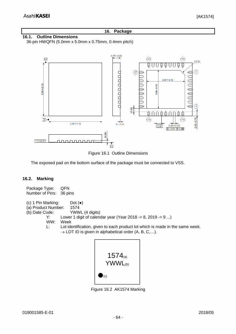
[AK1574]
018001585-E-01 2018/05 - 64 -
16. Package
16.1. Outline Dimensions 36-pin HWQFN (5.0mm x 5.0mm x 0.75mm, 0.4mm pitch)
Figure 16.1 Outline Dimensions
The exposed pad on the bottom surface of the package must be connected to VSS.
16.2. Marking
Package Type: QFN Number of Pins: 36 pins (c) 1 Pin Marking: Dot () (a) Product Number: 1574 (b) Date Code: YWWL (4 digits)
Y: Lower 1 digit of calendar year (Year 2018 -> 8, 2019 -> 9 ...) WW: Week L: Lot identification, given to each product lot which is made in the same week.
LOT ID is given in alphabetical order (A, B, C,…).
Figure 16.2 AK1574 Marking
1574(a)
YWWL(b)
(c)

[AK1574]
018001585-E-01 2018/05 - 65 -
17. Ordering Guide
- AK1574 36-pin QFN (5.0mm x 5.0mm, 0.4mm pitch) - AKD1574 AK1574 Evaluation Board
18. Revision History
Date (Y/M/D) Revision Reason Page Contents
18/03/15 00 Initial Version
18/05/11 01 Correction of errors - Correct minor errors in expressions
[AK1574]
018001585-E-01 2018/05 - 66 -
IMPORTANT NOTICE
0. Asahi Kasei Microdevices Corporation (“AKM”) reserves the right to make changes to the information contained in this document without notice. When you consider any use or application of AKM product stipulated in this document (“Product”), please make inquiries the sales office of AKM or authorized distributors as to current status of the Products.
1. All information included in this document are provided only to illustrate the operation and application examples of AKM Products. AKM neither makes warranties or representations with respect to the accuracy or completeness of the information contained in this document nor grants any license to any intellectual property rights or any other rights of AKM or any third party with respect to the information in this document. You are fully responsible for use of such information contained in this document in your product design or applications. AKM ASSUMES NO LIABILITY FOR ANY LOSSES INCURRED BY YOU OR THIRD PARTIES ARISING FROM THE USE OF SUCH INFORMATION IN YOUR PRODUCT DESIGN OR APPLICATIONS.
2. The Product is neither intended nor warranted for use in equipment or systems that require extraordinarily high levels of quality and/or reliability and/or a malfunction or failure of which may cause loss of human life, bodily injury, serious property damage or serious public impact, including but not limited to, equipment used in nuclear facilities, equipment used in the aerospace industry, medical equipment, equipment used for automobiles, trains, ships and other transportation, traffic signaling equipment, equipment used to control combustions or explosions, safety devices, elevators and escalators, devices related to electric power, and equipment used in finance-related fields. Do not use Product for the above use unless specifically agreed by AKM in writing.
3. Though AKM works continually to improve the Product’s quality and reliability, you are responsible for complying with safety standards and for providing adequate designs and safeguards for your hardware, software and systems which minimize risk and avoid situations in which a malfunction or failure of the Product could cause loss of human life, bodily injury or damage to property, including data loss or corruption.
4. Do not use or otherwise make available the Product or related technology or any information contained in this document for any military purposes, including without limitation, for the design, development, use, stockpiling or manufacturing of nuclear, chemical, or biological weapons or missile technology products (mass destruction weapons). When exporting the Products or related technology or any information contained in this document, you should comply with the applicable export control laws and regulations and follow the procedures required by such laws and regulations. The Products and related technology may not be used for or incorporated into any products or systems whose manufacture, use, or sale is prohibited under any applicable domestic or foreign laws or regulations.
5. Please contact AKM sales representative for details as to environmental matters such as the RoHS compatibility of the Product. Please use the Product in compliance with all applicable laws and regulations that regulate the inclusion or use of controlled substances, including without limitation, the EU RoHS Directive. AKM assumes no liability for damages or losses occurring as a result of noncompliance with applicable laws and regulations.
6. Resale of the Product with provisions different from the statement and/or technical features set forth in this document shall immediately void any warranty granted by AKM for the Product and shall not create or extend in any manner whatsoever, any liability of AKM.
7. This document may not be reproduced or duplicated, in any form, in whole or in part, without prior written consent of AKM.