austriamicrosystems AG is now ams AG - Digi-Key Sheets/Austriamicrosystems PDFs... ·...
77
austriamicrosystems AG is now ams AG The technical content of this austriamicrosystems datasheet is still valid. Contact information: Headquarters: ams AG Tobelbaderstrasse 30 8141 Unterpremstaetten, Austria Tel: +43 (0) 3136 500 0 e-Mail: [email protected] Please visit our website at www.ams.com
Transcript of austriamicrosystems AG is now ams AG - Digi-Key Sheets/Austriamicrosystems PDFs... ·...

austriamicrosystems AG
is now
ams AG The technical content of this austriamicrosystems datasheet is still valid.
Contact information:
Headquarters: ams AG
Tobelbaderstrasse 30
8141 Unterpremstaetten, Austria
Tel: +43 (0) 3136 500 0
e-Mail: [email protected]
Please visit our website at www.ams.com

AS3604Multi-Standard Power Management Unit
aus t r iamic rosys tems
Data Sheet
id
1 General DescriptionThe AS3604 is a highly-integrated CMOS power manage-ment device designed specifically for portable devices such as mobile phones, PDAs, CD players, digital cam-eras and other devices powered by 1-cell lithium-based or 3- to 4-cell nickel-based batteries. It can be used for any mobile phone handset standards such as CDMA, WCDMA, GSM, GPRS, EDGE, UTMS and other Japa-nese or American standards.The device incorporates low dropout regulators (LDOs), DC/DC converters, a complete battery charger, and an audio power amplifier onto one die.
The linear analog LDOs feature extremely high perfor-mance regarding:
Noise – typ 30µVRMS from 100Hz to 100kHzLine/Load Regulation – < 1mV static, < 10mV transientPower Supply Rejection – > 70dB @ 1kHz
The integrated Step Down DC/DC Converter does not require an external Schottky diode yet provides very high efficiency (up to 95%) throughout the whole operating range. It can be either used as a stand-alone device or as a pre-regulator for LDOs to increase overall device effi-ciency.
A Step Up DC/DC Converter is included to supply power for white LEDs, together with programmable current sources to control LED brightness.
A low-distortion audio power amplifier (1 Watt @ 8Ω) sup-ports handsfree operation and HiFi ring-tones.
The device also features a chemistry-independent battery charger including automatic trickle charging, gas gauge, and programmable constant voltage and current charging.
The AS3604 is controlled via a serial interface and inte-grates all necessary system specific functions such as Reset, Watchdog, and Power-On Detection.
Output voltages and start-up timings can be programmed on metal-mask level, by register or by an external resistor.
2 Key FeaturesTen Programmable High Performance LDOs- Two Digital Low-Power LDOs (0.75 to 2.5V, 200mA;
250mA up to 1.4V) - Three RF Low-Noise LDOs (1.85 to 3.4V, 200mA) - Two RF Low-Noise LDOs (1.85 to 3.4V, 150mA;
200mA up to 2.6V) - One SIM Low-Power LDO (1.8 to 3.0V, 20mA) - One Periphery Low-Noise LDO (2.5 to 3.2V, 200mA)- One Low-Power LDO (2.5V, 10mA)
Programmable High Efficiency DC/DC Converters- Step Down: 0.8 to 3.4V, up to 500mA with 2.2MHz
Operating Frequency and Small External Coil (2.2µH)
- Step Up: 15V, 45mA, (for White LEDs)Stereo Audio Power Amplifier- 0.5W @ 4Ω – Stereo; 1W @ 8Ω – Bridged- Digital Volume Control, 3dB Steps- Click- and Pop-Less Start-Up and Power-Down
Complete Chemistry-Independent Battery Charger- Integrated Gas Gauge- Automatic Trickle Charging- Programmable Constant Current Charging- Programmable Constant Voltage Charging- Pulse Charging- Safety Functions (Low Battery Shutdown)- Over- and Under-Temperature Charge Disable- Operation without Battery- Can Regulate the Current Through the Battery or
from the Charger - Charger Input Overvoltage Protection (6V) - Shutdown even with Connected Charger - Charger Resume Operation - Charger Interrupts (Inserted, Removed, Overvolt-
age, Resume) - No-Battery Detection
Momentary Power Loss Detection - Battery Supply Short-Interruption Detection
(<200ms); (e.g., due to a dropped phone) Four Programmable Current Sources - 8-Bit (0.625 to 160mA) - Buzzer- Vibrator- LEDs
Wide Battery Supply Range 3.0 to 5.5VFour General Purpose Switches (1Ω and 2Ω)Three Programmable General Purpose I/O Pins On-Chip Bandgap Tuning for High Accuracy (±1%)Integrated Programmable Watchdog (7.5 to 1900ms)Programmable Reset (10 to 110ms)Shutdown Current typ 7µA (2.5V Always On)Overcurrent and Thermal Protection0.35µ CMOS Solution2.1 Watt Power Dissipation @ SCSB = 70ºC48-pin, 6x6mm QFN Package (0.4mm pitch)
3 ApplicationsMulti-standard power management for mobile phones, PDAs, and any other 1-cell Li+ or 3- to 4-cell NiMh pow-ered devices.
ams A
G
Technica
l conten
t still
val
www.austriamicrosystems.com Revision 1.22 1 - 76

AS3604 aust r iamicrosys temsData Sheet
ge Pump
bandog
.5V
band
smitter
iver
.5V
O
hesizer
witch
ory
band (Alternate)
Baseband Peripherals
T 3.0-5.5V
lid
4 Block DiagramsFigure 1. AS3604 Block Diagram. Option: Audio Amplifier In Differential Mode, Step Down DC/DC Converter as
Pre-Regulator for Digital LDOs
Note: Refer to Table 38 on page 74 for specifications of external components.
2.2µH
V2_5
AS3604Power Management
Unit
Charge Pump4.74-5.25V
30mA
Analog LDOLow Noise2.5-3.2V200mA
Analog LDOLow Noise1.85-3.4V
200mA
RF LDOLow Noise1.85-3.4V
200mA
RF LDOLow Noise1.85-3.4V
200mA
RF LDOLow Noise1.85-3.4V
200mA
RF LDOLow Noise1.85-3.4V
200mA
Step Up DC/DC Converter
≤15V45mACurrent Source
4x(0.6-160mA)
L122µH
VBAT
CAPP CAPN
32
C2330nF
V5_6CharC3
1µF
C41µF
C61µF
C81µF
C91µF
C131µF
BaseAnal
3.0-5
BaseCore
RFTran
RFRece
3.0-5
VBAT
VCOTXC
Syntetc.
Internal LDO2.5V, 10mA
C51µF
C722µF
C101µF
C121µF
V2_5ON S
Interrupt, LCD Control, etc.
Digital LDO0.75-2.5V
250mA
SIM LDO3.0V, 20mA
C111µF
Digital LDO0.75-2.5V
250mA
Step Down DC/DC Converter
1.0-3.0V, 500mA
C141µF
C151µF
FlashMem
BaseCore
LX48
C161µF
C1810µF
C19100nF
SIM Card
POR
VANA_1
Digital Logic and References
BootROM
R7RPROGRAM
R6220kΩ
C29100nF
242623
RPROGRAMCREFRBIAS
10
RESET
R5100kΩ
RESET
VANA_1
I/F
SerialInterface
V2_5 or VBAT
NiMh, LiIon
Battery Charger and Gas Gauge
R34.7kΩ
R24.7kΩ
C27
R450mΩ
C281µF
Li-IonNiMh
VBATAll caps on VBAT ≥10µF total
Pad
GND_PAD
C261µF R1
2kΩ
DC Char-ger
Adapter ≤15V
≥8ΩLS1
1W Audio Amplifier
C23100nF
C24100nF
AudioIn
C25100nF
VBATC221µF
C11µF
STEPUP
36
D1MBR0520
WhiteLEDsVibratorBuzzer
CURR1
35343332
CURR2CURR3CURR4
VSIM46
Feedback
Q1Si3441
VBA
L2
VBAT_247
VBUCK40
VDIG_239
VDIG_141
V2_522
VRF_419
VBAT_518
VRF_317
VRF_27
VBAT_48
VRF_19
VANA_26
VBAT_15
VANA_14
V5_61
VBAT_3 30
AOUT_L 28
AIN_L 38
AGND 31
AIN_R 37
AOUT_R 29
VCHARGER 20
VGATE 21
ISENSP 15
ISENSN 16
GND_SENSE 27
ON 25
SDI 12
SCLK 13
SDO 11
SCSB 14
GPIO
VANA_1
V5_6
GPIO343
GPIO244
GPIO145
VBAT_642VBAT 3.0-5.5V
ams A
G
Technica
l conten
t still
va
www.austriamicrosystems.com Revision 1.22 2 - 76

AS3604 aust r iamicrosys temsData Sheet
ge Pump
bandog
.5V
band
smitter
iver
.5V
O
hesizer
witch
pt, LCD l, etc.
lash emory
aseband ore
Alternative)
.0-5.5V
aseband eripherals
lid
Figure 2. AS3604 Block Diagram. Option: Audio Amplifier in Stereo Single-Ended Mode, Digital LDOs Separated from Step Down DC/DC Converter
Note: Refer to Table 38 on page 74 for specifications of external components.
NiMh, LiIon
Battery Charger and Fuel Gauge
AS3604Power Management
Unit
Charge Pump4.74-5.25V
30mA
Analog LDOLow Noise2.5-3.2V200mA
Analog LDOLow Noise1.85-3.4V
200mA
RF LDOLow Noise1.85-3.4V
200mA
RF LDOLow Noise1.85-3.4V
200mA
RF LDOLow Noise1.85-3.4V
200mA
RF LDOLow Noise1.85-3.4V
200mA
Step Up DC/DC Converter
≤15V45mACurrent Source
4x(0.6-160mA)
L122µH
VBAT
CAPP CAPN
32
C2330nF
V5_6CharC3
1µF
BaseAnal
3.0-5
BaseCore
RFTran
RFRece
GPIO
3.0-5
VBAT
VCOTXC
Syntetc.
Internal LDO2.5V10mA
V2_5ON S
InterruContro
VANA_1
V5_6
Digital LDO0.75-2.5V
250mA
SIM LDO3.0V, 20mA
Digital LDO0.75-2.5V
250mA
Step Down DC/DC Converter
1.0-3.0V, 500mA
FM
3.0-5.5V
SIM Card
POR
VANA_1
Digital Logic and References
BootROM
10
RESET
R5100kΩ
RESET
VANA_1
I/F
SerialInterface
V2_5 or VBAT
R34.7kΩ
R24.7kΩ
C27
R450mΩ
C281µF
Li-IonNiMh
VBATAll capson VBAT
≥10µFtotal
C261µF
R12kΩ
DC Char-ger
Adapter ≤15V
≥4ΩLS2 1W Audio
Amplifier
C20≥100µF
C21≥100µF
IN_L
VBATC221µF
C11µF
STEPUP
36
D1MBR0520
WhiteLEDsVibratorBuzzer
CURR1
35343332
CURR2CURR3CURR4
V2_5
1.0-5.5VFeedback
Q1Si3441
≥4ΩLS3
IN_R
C23100nF
C25100nF
BC(
C24100nF
R7RPROGRAM
R6220kΩ
C29100nF
242623
RPROGRAMCREFRBIAS Pad
GND_PAD
C41µF
C51µF
C101µF
C91µF
C111µF
C121µF
C131µF
C19100nF
C301µF
C722µF
C141µF
VBAT_3 30
AOUT_L 28
AIN_L 38
AGND 31
AIN_R 37
AOUT_R 29
VCHARGER 20
VGATE 21
ISENSP 15
ISENSN 16
GND_SENSE 27
ON 25
SDI 12
SCLK 13
SDO 11
SCSB 14
LX48
VSIM46
VBAT_247
VBUCK40
VDIG_239
VDIG_141
GPIO343
GPIO244
GPIO145
V2_522
VRF_419
VBAT_518
VRF_317
VRF_27
VBAT_48
VRF_19
VANA_26
VBAT_15
VANA_14
V5_61
C61µF
C81µF
C151µF
VBAT_642VBAT 3
2.2µHC161µF
C1810µF
BP
L2
ams A
G
Technica
l conten
t still
va
www.austriamicrosystems.com Revision 1.22 3 - 76

AS3604 aust r iamicrosys temsData Sheet
lid
Content1 General Description ..............................................................................................................................12 Key Features .........................................................................................................................................13 Applications ...........................................................................................................................................14 Block Diagrams .....................................................................................................................................25 Absolute Maximum Ratings (Non-Operating) .......................................................................................6
5.1 Operating Conditions .....................................................................................................................................66 Detailed Functional Descriptions ..........................................................................................................7
6.1 Battery Charger Controller .............................................................................................................................76.2 Step Down DC/DC Converter ......................................................................................................................246.3 Low Dropout Regulators ..............................................................................................................................306.4 Charge Pump ...............................................................................................................................................416.5 Step Up DC/DC Converter ...........................................................................................................................426.6 General Purpose Input/Output .....................................................................................................................446.7 Current Sinks ...............................................................................................................................................506.8 Audio Amplifier .............................................................................................................................................53
7 System Supervisory Functions ...........................................................................................................567.1 Reset ...........................................................................................................................................................567.2 Startup ..........................................................................................................................................................587.3 Protection Functions ....................................................................................................................................597.4 Watchdog Block ...........................................................................................................................................607.5 Internal Reference Circuits ..........................................................................................................................617.6 Low Power Mode .........................................................................................................................................637.7 Boot Sequence Detection ............................................................................................................................637.8 Serial Interface .............................................................................................................................................64
8 Register Map .......................................................................................................................................689 Pinout and Packaging .........................................................................................................................70
9.1 Pin Descriptions ...........................................................................................................................................709.2 Package Drawings and Markings ................................................................................................................72
10 External Parts List .............................................................................................................................7411 Ordering Information .........................................................................................................................75
ams A
G
Technica
l conten
t still
va
www.austriamicrosystems.com Revision 1.22 4 - 76

AS3604 aust r iamicrosys temsData Sheet
lid
Revision History
Revision Date Owner Description1.0 23 June 2006 ptr - Initial release.
1.1 3 March 2007 ptr - Updated ambient temperature range.
1.11 4 Dec 2008 pkm - Updated internal LDO supply description
1.2 8 Apr 2009 pkm - Updated ordering info for AS3604B chip version
1.21 15 Mai 2009 pkm - Updated abs. max ratings and stand-by current, deleted errata
1.22 21 Aug 2009 pkm - Updated operating current, SNR and VCHOV
ams A
G
Technica
l conten
t still
va
www.austriamicrosystems.com Revision 1.22 5 - 76

AS3604 aust r iamicrosys temsData Sheet
lid
5 Absolute Maximum Ratings (Non-Operating)Stresses beyond the absolute maximum ratings may cause permanent damage to the AS3604. These are stress rat-ings only. Functional operation of the device at these or beyond those in Operating Conditions is not implied.
Caution: Exposure to absolute maximum rating conditions may affect device reliability.
5.1 Operating Conditions
Table 1. Absolute Maximum Ratings
Symbol Parameter Min Max Unit Notes
VIN_HV High Voltage Pins -0.3 18.0 V Applicable for high voltage pins: VCHARGER, VGATE, and STEPUP
VIN_MV 5V Pins -0.3 7.0 V
Applicable for pins 5V pins: VBAT_1 - VBAT_6, V5_6, VBUCK, GPIO1 - GPIO3, CURR1 - CURR4, AIN_L, AIN_R, AOUT_L, AOUT_R, VRF_1 - VRF_4 (when not in LDO-mode), ON, and LX
VIN_LV 3.3V Pins -0.3 5.0 V
Applicable for 3.3V pins: RESET, SCSB, SCLK, SDI, SDO, VANA_1, VANA_2, VSIM, VDIG_1, VDIG_2, CAPN, AGND, ISENSP, ISENSN, V2_5, CREF, RBIAS, and RPROGRAM
IIN Input Pin Current -25 +25 mA At 25ºC Norm: JEDEC 17
Tstrg Storage Temperature Range -55 125 ºC
Humidity 5 85 % Non-condensing
VESD Electrostatic Discharge -1000 1000 V Norm: MIL 883 E Method 3015; ±1000V.
PT Total Power Dissipation 2.1 W TAMB = 70ºC
Tmax Peak Reflow Soldering Temperature 260 ºC T = 20 to 40s, according to the IPC/JEDEC J-
STD 020C.
Table 2. Operating Conditions
Symbol Parameter Min Typ Max Unit Notes
VHV High Voltage 0.0 15.0 V Pins VCHARGER, VGATE and STEPUP
VBAT Battery Voltage 3.0 3.6 5.5 VFor pins VBAT_1 - VBAT_6. During startup from ext. battery charger adapter, the battery voltage can be below 3.0V.
VANA_1 Periphery Supply Voltage (for RESET and SPI pins) 2.5 Boot
ROM 3.2 V Internally generated from VANA_1.
VON Activation voltage for ON pin 1.75 V2_5 VBAT V
V2_5 Voltage on Pin V2_5 2.4 2.5 2.6 V Internally generated.
V5_6 Output Voltage of Charge Pump 5.0 5.2 5.6 V 2 x VANA_1
TAMB Ambient Temperature -40 25 85 ºC
IBAT Operating Current 195 260 µANormal operating current. With bit low_power_on (page 62) = 0; only VANA_1 active, no additional external loads.
ILOWPOWERLow-Power Mode Current
Consumption 110 µAWith bit low_power_on (page 62) = 1; only VANA_1 active, no additional external loads.
IPOWEROFF Power-Off Mode Current Consumption 13 20 µA
With bit power_off (page 57) = 1; only V2_5 is active in power off mode.not tested, guaranteed by design
ams A
G
Technica
l conten
t still
va
www.austriamicrosystems.com Revision 1.22 6 - 76

AS3604 aust r iamicrosys temsData Sheet
lid
6 Detailed Functional Descriptions6.1 Battery Charger ControllerThe AS3604 can serve as a standalone Battery Charger Controller supporting rechargeable lithium-ion (Li+), lithium-polymer (LiPo) and 3- or 4-cell nickel metal-hydride (NiMh) batteries.
The main features of the Battery Charger Controller are:
Constant Voltage Charge Mode – Described on page 9 Pulse Charge Mode – Described on page 11 Battery Presence Detection – Described on page 14 Operation Without Battery – Described on page 14 Charge Controller Bypass – Described on page 14 Overvoltage and Undervoltage Supervision – Described on page 15
Figure 3. Battery Charger Controller Block Diagram
Table 3. Battery Charger Controller Components
Symbol Parameter Value Notes
MCHG P-Channel MOSFET Si3441BDV, Si8401DB or similar
The maximum power dissipation of this transistor is not limited by the AS3604.
RPUP Pull-Up Resistor 2KΩ ± 5%
RSENSE Current Sense Resistor 50mΩ ± 1%, 125mW for IVBAT,DC < 1.5A e.g. Vishay Dale WSL0805
RFILT1,2 Filter Resistor 47KΩ ± 1% Can be omitted if Gas Gauge functionality is not used (RFILT1,2 = 0Ω)CFILT Filter Capacitor 100nF ± 20%, X5R or
X7R Dielectric
CCHRG Bypass Capacitor on pin VCHARGER
1µF ± 20%, X5R or X7R Dielectric
CBAT Minimum Total Capacitance Parallel to Battery 10µF
CBAT
VCHARGER
RSENSE
AS3604
Battery Charger Controller
VGATE
VBAT_5
ISENSP
ISENSN
VSS
RPUP
MCHG
RFILT1BATT
GND_PCB
VBAT
Charger
CCHRG
CFILTRFILT2
ams A
G
Technica
l conten
t still
va
www.austriamicrosystems.com Revision 1.22 7 - 76

AS3604 aust r iamicrosys temsData Sheet Bat tery Charger Cont ro l le r
lid
6.1.1 Low-Current Trickle Charge ModeLow-Current Trickle Charge mode is initiated when an external battery charger has been detected, bit chDet (page 19) = 1, and the battery voltage is below the VUVLO threshold; bits ChAct (page 19) and Trickle (page 19) will be set. In Trickle Charge mode the charge current will be limited to the value specified by Trickle Current (page 21) to prevent undue stress on either the battery or the Battery Charger in case of deeply discharged batteries.
Once VUVLO has been exceeded, the Battery Charger will terminate Trickle Charge mode (charger must not be dis-abled between trickle and constant current (fast) charging), reset bits ChAct and Trickle, and switch on the device.
The trickle charge is terminated in any case after approximately 60 minutes (as it is assumed that the battery is dam-aged in this case)
6.1.2 Constant Current Charge ModeConstant Current mode is initiated by setting bit ChEn (page 20) and resetting bit Fast (page 20). Bit ChAct (page 19) is set automatically when the Battery Charger starts. Charge current will be limited to the value specified by bit Constant Current (page 21) by the Battery Charger Controller.
6.1.3 Charging Nickel-based BatteriesFor nickel-based batteries (NiMh), BatType (page 20) must be 1 (see Figure 4 on page 9). The endpoint detection (ΔV/Δt) must be performed by the host controller. It must turn off the charger duly to avoid overcharging. In any case, when the battery voltage exceeds the charge termination threshold (typ. 5.5V), the charger will be turned off and bit EOC (page 20) will be set.
6.1.4 Charging Lithium-based BatteriesFor lithium-based batteries (Lithium-Ion, Lithium-Polymer), BatType (page 20) must be 0. Additionally, bit Li4v2 (page 20) can select between coke- and graphite-anode, setting different charge termination thresholds (typ. 4.1 or 4.2V). The charger is designed to charge 1-cell lithium-based batteries independently, using Trickle Charge, Constant Current, Constant Voltage, or Pulse Charge modes.
When the battery voltage exceeds the charge termination threshold during Constant Current mode, it automatically continues charging with either Constant Voltage mode, bit Pulse (page 20), or Pulse Charge mode, Pulse, and termi-nates when the end-of-charge conditions are met (see Figure 5 on page 11 and Figure 6 on page 13).
Table 4. Battery Charger Controller Parameters
Symbol Parameter Min Typ Max Unit Notes
VCHDET Charger Detection Threshold. VCHARGER - VBAT_5: Charger On 50 75 105 mV
Hysteresis = (VCHDET - VCHMIN)< 40mV
VCHMIN Charger Detection Threshold. VCHARGER - VBAT_5: Charger Off 5 20 35 mV
VCHREG Bootstrap Regulator Voltage 2.4 2.5 2.6 V VCHARGER > 5V
VCHOVHVCHARGER Overvoltage Detection
6.2 6.45 6,71V
Monitor voltage on VCHARGER and disable charging if this voltage is exceeded.VCHOV 5,81 6.05 6,29
VUVLO Undervoltage Lockout Threshold3.1
VVBAT rising
2.8 VBAT falling
VOVLO Overvoltage Lockout Threshold5.5
VVBAT rising
5.4 VBAT falling
VCHOFF Charge Termination Threshold
4.14 4.20 4.26
V
Li+ Battery: BatType (page 20) = 0, Li4v2 (page 20) = 1
4.05 4.1 4.15Li+ Battery: BatType = 0, Li4v2 = 0.From -5 to +50ºC
5.44 5.5 5.6 NiMh Battery: BatType = 1
VNOBATDET No-Battery Detection Threshold and Charger Resume Detection Threshold 3.644 V DisOWB (page 21) = 0
ams A
G
Technica
l conten
t still
va
www.austriamicrosystems.com Revision 1.22 8 - 76

AS3604 aust r iamicrosys temsData Sheet Bat tery Charger Cont ro l le r
lid
Figure 4. Startup and Constant Current Charging of Nickel-based Batteries
6.1.5 Fast Charge ModeAs an alternative to Constant Current mode, Fast Charge mode may be selected. The charge current will not be con-trolled in this mode and is only limited by the external battery charger adapter.
Fast Charge mode is initiated by setting bits ChEn (page 20) and Fast (page 20). Bit ChAct (page 19) is set when the Bat-tery Charger has started.
End of ChargeIn Fast Charge mode, the same charge termination thresholds apply as for Constant Current mode. Additionally, depending on bit Fast (page 20), the current during pulse charging is either the selected constant current or maximum. Charging will resume if the battery voltage drops below VNOBATDET.
6.1.6 Constant Voltage Charge ModeConstant Voltage mode is initiated and bit CVM (page 19) will be set when threshold VCHOFF (page 8) has been exceeded for the first time (no debounce filter) and bit Pulse (page 20) is not set.
External Charger at Pin VCHARGER
Principle Only. Not To Scale.
VBAT
ICHARGE Trickle CurrentConstant Current or Fast Current
VUVLO3.1V
VCHDET
0V
Power up LDOs = Boot ROM
LDOVoltages
Serial Communication Possible
Reset
Register Settings (Write)
ChEnµC: Activate
ChargerμC: Turn Off Charger
Pulse
ChDet
Register Settings (Read)
Trickle
ChAct
CVM
EOC
Trickle Charge Mode Power Up; No Charge
Constant Current Mode Bit EOC is only set when VCHOFF is exceeded
t = 0
6-11mst
10-110ms
ΔV/ΔI Detection by External ADC
VCHOFF = 5.5V(BatType = 1)
CC Charging Terminates Immediately when VCHOFF is exceeded
BatType
µC: SelectBattery Type
ams A
G
Technica
l conten
t still
va
www.austriamicrosystems.com Revision 1.22 9 - 76

AS3604 aust r iamicrosys temsData Sheet Bat tery Charger Cont ro l le r
lid
The charge controller will regulate the battery voltage to a value set by bit Li4v2 (page 20). To enable operation of the device without a battery connected to the system it is necessary that the charger is not disabled between the moment when the VCHOFF threshold is exceeded for the first time and the beginning of constant voltage charge mode.
During Constant Voltage mode, the charge current will decrease and eventually drop below the value set by Trickle Current (page 21). If the measured charge current is less than or equal to Trickle Current, charging is terminated and bit EOC is set. Charging will resume if the battery voltage drops below VNOBATDET.If the battery has been removed during constant voltage charging the EOC condition and the no battery condition will probably conflict. To be able to properly detect the EOC state the EOC condition has to be dominant over the no battery condition.If the battery voltage (VBAT_5) drops below VNOBATDETECT (page 8) (signal resume starts pulsing), e.g. if the bat-tery is removed after charging is finished, EOC (page 20) will be cleared (after debounce time) and the battery char-ger controller will resume in constant voltage mode to enable operation of the device without battery. This only works if bit CVM (page 19) remains set when bit EOC is set, otherwise the comparators that are required for operation without battery are gated.
Three scenarios are possible at this point:
1. If a battery is connected the charge current will now be high and charging will return to constant current charg-ing.
2. No battery is connected and no current will flow through the sense resistor. Now the no battery condition is detected properly.
3. The battery was connected and is disconnected. No current will flow through the sense resistor and the no bat-tery condition is detected properly. In summary: When charging is resumed after an EOC state either a (dis)charge current will be measured and the charge controller will return to constant current mode or no current will be measured and a “no battery” condition is indicated. To be able to handle supply voltage spikes caused by e.g. battery bouncing when the system is heavily shaken the VNOBATDETECT detection has to be debounced for 1 current measurement cycle before EOC is cleared. After the debounce time is over additional pulses must occur during the next current measurement cycle to clear EOC.The no battery status is indicated with bit NoBat (page 20).
If the battery is replaced after charging is finished and the charge current exceeds the value set by Constant Current (page 21), the charge controller will clear bit CVM and return to Constant Current or Fast Charge mode, depend-ing on bit Fast (page 20).
Notes:1. Bit CVM will be ambiguous if bit Fast is set.2. EOC will only be entered if bit AutoChgTerm (page 21) is set (default = 0).
ams A
G
Technica
l conten
t still
va
www.austriamicrosystems.com Revision 1.22 10 - 76

AS3604 aust r iamicrosys temsData Sheet Bat tery Charger Cont ro l le r
lid
Figure 5. Startup and Constant Voltage Charging of Lithium-based Batteries
6.1.7 Pulse Charge ModePulse Charge mode is initiated and bit CVM (page 19) will be set when the VCHOFF (page 8) threshold has been exceeded for the first time and bit Pulse (page 20) is set. If the battery voltage is below the VCHOFF threshold, the Bat-tery Charger will be enabled for a minimum on-time specified by bit TPON (page 21).
If the battery voltage drops below VCHOFF at the end of the minimum on-time, the Battery Charger will remain switched on until the battery voltage exceeds VCHOFF. The Battery Charger will then be disabled for at least the minimum off-time specified by bit TPOFF (page 21), and the Battery Charger will only be switched on again when the battery voltage falls below VCHOFF. In any case, whenever the instantaneous battery voltage exceeds the overvoltage lockout thresh-old VOVLO, charging is disabled immediately.
External Charger at Pin VCHARGER
Principle Only. Not To Scale.
VBAT
ICHARGE Trickle Current
Constant Current or Fast Current
VUVLO3.1V
VCHDET
0V
Power up LDOs = Boot ROM
LDOVoltages
Serial Communication Possible
Reset
Register Settings (Write)
ChEnµC: Activate
Charger
µC: Turn Off Charger
Pulse
ChDet
Register Settings (Read)
Trickle
ChAct
CVM
EOC
Trickle Charge Mode Power Up; No Charge
Constant Current Mode
t = 0
6-11mst
10-110ms
VCHOFF
4.2V Graphite Anode (Li4v2 = 1)4.1V Coke Anode (Li4v2 = 0)
BatType
CV Charge Terminates when Charge Current drops below Trickle Current
Constant Voltage Mode
ams A
G
Technica
l conten
t still
va
www.austriamicrosystems.com Revision 1.22 11 - 76

AS3604 aust r iamicrosys temsData Sheet Bat tery Charger Cont ro l le r
lid
During on-pulses, the charge current will be limited to the value set by Constant Current (page 21) if bit Fast (page 20) = 0. If bit Fast = 1, the charger transistor Q1 (page 2) will be fully on and the charge current during on-pulses will only be limited by the external charge adapter.
At the beginning of a Pulse Charge cycle, the Battery Charger will operate at a duty cycle close to 100%. Toward the end of the Pulse Charge cycle the Battery Charger will be switched off for long periods between short on-pulses. Even-tually, the off-time will become longer than the value specified by bit TPOFFMAX (page 21), and the charging cycle will terminate (bit EOC (page 20) is set). Charging will resume if the battery voltage drops below VNOBATDET.
If the battery voltage drops below VNOBATDETECT (page 8), e.g. if the battery is removed after charging is finished, EOC (page 20) will be cleared and the battery charger controller will resume in pulse charge mode to enable operation of the device without battery. The no battery status is indicated with bit NoBat (page 20).
If the battery is replaced after charging is finished and the on-pulse duration TPON (page 21) becomes longer than TPOFFMAX (page 21), the charge controller will clear bit CVM (page 19) and return to Constant Current or Fast Charge mode, depending on bit Fast (page 20).
Note: With TPOFFMAX = 11 (no termination), the condition for returning to Constant Current or Fast Charge mode will never be met. Bit CVM will be ambiguous in this case.
If AutoChgTerm (page 21) is 0, the battery continues to be charged after EOC.
During on-pulses the instantaneous battery voltage may exceed VCHOFF by several hundred millivolts. However, no harm will be done to the battery if TPON (page 21) is selected to be shorter than the electrochemical time constant of the battery.
By adding an external gate-source capacitor the switching edges of the P-channel MOSFET can be slowed down fur-ther. This prevents an external battery charge adapter with poor transient response from subjecting the VCHARGER pin to excessive voltage when the P-channel MOSFET turns off, and prevents excessive current into the battery when the P-channel MOSFET turns on.
ams A
G
Technica
l conten
t still
va
www.austriamicrosystems.com Revision 1.22 12 - 76

AS3604 aust r iamicrosys temsData Sheet Bat tery Charger Cont ro l le r
: turn offrger
t
when
lid
Figure 6. Startup and Pulse Charging for Lithium-Based Batteries
µCcha
EOC
CVM
Trickle
Register Settings (Read)
Register Settings (Write)
Pulse
ChEn
tpon
tpoff(min)
VBAT
External Char-ger at Pin VCHARGER
VCHDET
VCHOFF:4.2V Graphite Anode (Li4v2 = 1)4.1V Coke Anode (Li4v2 = 0)
ICHARGETrickle Current
Constant Current or Fast Current
VUVLO3.1V
Power up LDOs = Boot ROM
LDOVoltages
t = 0
6-11ms
tpoff extends until VBAT falls below VCHOFF
If tpoff ≥tpoffmax:EOC
Reset
BatType
Serial Communication Possible
10-110ms
ChDet
ChAct
µC: ActivateCharger
Trickle Charge Mode Power Up; No Charge
Constant Current Mode
Pulse Charge Mode Bit EOC is settpoff≥tpoffmax
Principle Only. Not To Scale.
ams A
G
Technica
l conten
t still
va
www.austriamicrosystems.com Revision 1.22 13 - 76

AS3604 aust r iamicrosys temsData Sheet Bat tery Charger Cont ro l le r
lid
6.1.8 Battery Presence DetectionWhen active, the charge controller constantly monitors the voltage drop across an external current sense resistor (RSENSE) connected in series between the negative battery terminal and ground. In case no battery is connected to the system, no current can flow through RSENSE. If no (dis)charge current flow is detected, bits NoBat (page 20) and CVM (page 19) will be set.
If a battery is re-connected to the system, current will be flowing through Rsense. If a (dis)charge current flow is detected, NoBat and CVM will be cleared. Battery presence indication can be disabled by setting bit DisBDet (page 21).
6.1.9 Operation Without BatteryThis feature allows operation of the device without a battery if a charge adapter is applied to the VCHARGER pin and bit ChEn (page 20) is set. The battery voltage is regulated to the charge termination threshold VCHOFF (page 8), depend-ing on the setting of bits BatType (page 20) and Li4v2 (page 20).
Note that when the charge controller is disabled by clearing bit ChEn e.g., during measurement of the battery voltage by an external ADC, the device will be reset when the battery is removed. The “operation without battery” feature can be disabled by setting DisOWB (page 21). The minimum required capacitance on VBAT (all buffer caps combined) must be ≥10µF to reduce the ripple on VBAT when operating the AS3604 without battery.
6.1.10 Charge Controller BypassThe charge controller can be bypassed by setting bit Bypass (page 20). In bypass mode, the charger transistor Q1 (page 2) is fully on. The overvoltage protection however will turn off the transistor, when VBAT ≥ VOVLO (page 8). End-of-charge detection is disabled and has to be performed by the system host, bit EOC is cleared.
Removal of the charge adapter will be indicated in the Charger Status Register (page 19) but the charge controller will not be disabled. This feature is especially useful when using current-limited charge adapters with an output voltage close to the charge termination threshold and the system is operating without battery. Note that when the voltage differ-ence between the charge adapter output voltage and the battery is smaller than VCHMIN (page 8) the charger detection circuit will indicate that no charge adapter is connected. Furthermore, Trickle Charge mode is not supported in bypass mode because the current regulation is overruled by bit Bypass.
ams A
G
Technica
l conten
t still
va
www.austriamicrosystems.com Revision 1.22 14 - 76

AS3604 aust r iamicrosys temsData Sheet Bat tery Charger Cont ro l le r
lid
Figure 7. Battery Charger Flow Chart
6.1.11 Overvoltage and Undervoltage SupervisionWhen the battery voltage exceeds the VOVLO (page 8) threshold (VBAT rising), the charger transistor Q1(page 2) is turned off. Charging will resume if the battery voltage drops below VOVLO (VBAT falling).
Likewise, when the battery voltage drops below the Undervoltage Lockout Threshold VUVLO (VBAT falling) (page 8), a Reset is generated (page 56), which also clears bit ChEn (page 20).
The charger will remain in low current Trickle Charge mode (page 8) until the VUVLO threshold (VBAT rising) has been exceeded.
If ChOv (page 21) =1, the AS3604 monitors the voltage on pin VCHARGER. If the voltage on VCHARGER exceeds VCHOV (bit ChOvH (page 21) = 0) or VCHOVH (bit ChOvH =1) the Battery Charger stops. If the voltage subsequently drops below this limit, the Battery Charger automatically resumes charging.
Non-ChargingMode
Chargerdetected?
VBAT>VUVLO?
Trickle Charge
NO
YES ChDet=1
Chargerdetected?
ChAct=1;Trickle=1
ChDet=0;ChAct=0;Trickle=0
Device active?
NO
NO
NO
VBAT>VUVLO?
Startup Device
YES
YES Trickle=0
NO
YES
Active ChargingMode
Chargerdetected?
ChEn=1?
YES NO
NO
ChDet=0;ChAct=0
YES
Fast Charge / ConstantCurrent Charge
YES
Chargerdetected?
VBAT>VCHOFF?
NO
BatType=1?
YES
EOC = 1
YES
Top-Off Charge
Chargingcomplete?
ChEn=1?
Chargerdetected?
ChEn = 0
ChAct=1
ChAct=0;EOC=0;(CVM=0)
YES
YES
YES
ChEn=1?
YES
YES
NO
NO
ChAct=0
CVM=1
NO
NO
NO
ChAct=0;CVM=0
NO
ChDet=0;ChAct=0
ChDet=0;ChAct=0;CVM=0
ChAct=0
V BAT
< V
NO
BATD
ET
EOC=0
ams A
G
Technica
l conten
t still
va
www.austriamicrosystems.com Revision 1.22 15 - 76

AS3604 aust r iamicrosys temsData Sheet Bat tery Charger Cont ro l le r
lid
6.1.12 Charger Detection CircuitThe Battery Charger Controller uses an integrated Charger Detection Circuit to determine if an external battery char-ger adapter has been applied to pin VCHARGER.
Charger register bits will be set/reset when any of the following conditions are met:
1. When the charger voltage exceeds the battery voltage by VCHDET (page 8), Bit chDet (page 19) will be set. 2. When the charger voltage drops below VCHMIN (page 8) above the battery voltage, bit chDet will be reset. If the
charger was active, bit ChEn (page 20) = 1, bit ChAct (page 19) will also be reset. Charging will resume when the conditions for bit chDet = 1 are met.
3. If a Reset occurs during charging, the charger will also be reset (ChAct = 0). Bits ChEn and chDet will remain set to 1. To resume charging, the charger must be turned off (ChEn = 0) and then on (ChEn = 1).
6.1.13 Bootstrap Voltage RegulatorTo charge even completely discharged batteries, the AS3604 contains an internal bootstrap voltage regulator (LDO V2_5) which generates a bootstrap voltage (VCHREG) to supply power to the internal Battery Charger circuitry.
6.1.14 Battery Charger OperationThe Battery Charger Controller controls an 8-bit current DAC which delivers a current (IDAC) that will generate a volt-age (VGS) over an external resistor (RGS) connected between the gate and source of an external P-channel MOSFET.
Charge Current RegulatorThe Charge Current Regulator has a resolution of 0.625mV or 12.5mA when using a 50mΩ sense resistor. The resolu-tion is programmable using the Charger Control Register (page 20).
Note: Setting bit Boost (page 20) = 1 multiplies this current by a factor of 10.
6.1.15 Charger Total Current RegulationDuring normal operation, the AS3604 controls the charging current through the battery. Alternatively, it is possible to regulate the maximum current from the charger (see Figure 8).
If the shunt resistor is connected as shown in Figure 8 , the charger regulates the current from the charger adapter. The internal register bit AutoChgTerm (page 21) must be set to 0 in this configuration. If AutoChgTerm is reset, the char-ger is not switched off if an end-of-charge condition is reached (only an interrupt is sent to the baseband processor).
If the end-of-charge interrupt is sent to the baseband processor, the baseband processor can terminate the charging cycle by setting bit AutoChgTerm to 1. This should only be done if a battery is present. If bit AutoChgTerm is 1 and the battery is subsequently removed, the baseband processor should immediately reset bit AutoChgTerm to 0 and bit ChEn (page 20) should be set to 0 and then to 1 again to restart the charger and avoid a reset cycle of the system due to undervoltage condition on the battery.
To avoid a reset cycle of the system under any condition, bit AutoChgTerm’ should usually be left at 0.
Note: The AS3604 measures the current from the charger including the current used for charging the battery and the current flowing to the whole system. The end-of-charge detection is done by comparing this current against the value set in the bits Trickle Current (page 21). Therefore this value has to be set sufficiently high to obtain a proper end-of-charge condition. If this is not possible, a timeout timer inside the baseband processor should be set allowing for an end-of-charge indication in the user interface.
Table 5. Charge Current Regulator Parameters
Symbol Parameter Min Typ Max Unit
IVGATE,LSB Resolution of VGATE current; bit Boost (page 20) = 0 0.5 µA
IVGATE,FS Full-scale value of VGATE current; bit Boost = 0 127.5 µA
ams A
G
Technica
l conten
t still
va
www.austriamicrosystems.com Revision 1.22 16 - 76

AS3604 aust r iamicrosys temsData Sheet Bat tery Charger Cont ro l le r
lid
Figure 8. Total Current Regulation
6.1.16 Gas Gauge The Gas Gauge enables remaining capacity estimation of the battery by tracking the net current flow into and out of the battery using a Voltage-to-Frequency Converter.
Voltage-to-Frequency ConverterThe Voltage-to-Frequency Converter constantly monitors the voltage drop across an external current sense resistor (RSENSE) connected in series between the negative battery terminal and ground.
The use of an additional external RC lowpass filter is highly recommended. Using two 47kΩ resistors, R2 and R3 (page 2), and a 0.1µF ceramic capacitor, C28 (page 2), the filter cutoff is approximately 16.9 Hz. This filter will capture the effect of most spikes, and will thus allow the Gas Gauge to accurately detect the total charge that has gone into or out of the battery.
Charge Current Accumulator The Charge Current Accumulator is an internal 15-bit up/down counter with sign bit. It is incremented when current is charged into the battery and decremented when current is drawn out of the battery. It is updated at a rate of one count per 3.05µVh, which is equivalent to one count per 61.03µAh (using a 50mΩ current sense resistor).If the counter is not read, it will roll over beyond FFFFh, which occurs after approximately 2000mAh of charge (using a 50mΩ sense resistor). It is the responsibility of the host system to read and reset the counter before rollover occurs.
The contents of the Charge Current Accumulator will be transferred into the Delta Charge MSB Register (page 22) and the Delta Charge LSB Register (page 22) when bit UpdReq (page 22) has been set. After the Delta Charge MSB/LSB reg-isters have been updated successfully, bit UpdReq is cleared automatically and the Charge Current Accumulator will be reset along with bit sign.
Table 6. Gas Gauge Parameters
Symbol Parameter Min Typ Max Unit NotesfCLK Internal Reference Clock 1.0 1.1 1.2 MHzfVFC Sample Frequency fCLK/59 Hz fCLK: internal reference clock.
VISENSP/VISENSN Input Voltage -0.1 0.1 V
ZISENSP/ZISENSN Input Impedance 4.67 MΩ
AVFC (Dis)Charge Gain 91.0 Hz/VfCLK = 1.1MHz
FRVFC Fundamental Rate 3.05 µVhVOFF Uncompensated Offset Voltage -500 500 µV Offset voltage ISENSP - ISENSN
VOFF,COMP Compensated Offset Voltage -50 ±10 50 µV Offset error after offset compensation
LiIon, NiMhBattery Charger
R34.7kΩ
R24.7kΩ
C27
R450mΩ
C281µF
LiIonNiMh
VBAT
C261µF
R12kΩ
DC Char-ger
Adapter ≤15V
Q1Si3441
VCHARGER 20
VGATE 21
ISENSP 15
ISENSN 16
AS3604Power Management
Unit
GND_SENSE 27
All caps on VBAT≥10µF total
ON 25
VBAT orV2_5
ams A
G
Technica
l conten
t still
va
www.austriamicrosystems.com Revision 1.22 17 - 76

AS3604 aust r iamicrosys temsData Sheet Bat tery Charger Cont ro l le r
lid
Constant Voltage RegulatorThe Constant Voltage Regulator acts directly on the setting of the 8-bit current DAC. It will commence when threshold VCHOFF (page 8) has been exceeded for the first time as long as bit Pulse (page 20) is not set.
Elapsed Time CounterThe sample clock (fVFC) of the Gas Gauge is fed to a 14-bit clock count divider, whose output signal is used as a clock-ing signal for the 16-bit Elapsed Time Counter, resulting in an equivalent rate of 1.1379 counts per second (4096.60 counts = 1 hour, 1 count = 0.8788s).
The Elapsed Time Counter can rollover beyond FFFFh which occurs after about 16 hours. If this happens the value given by the counter will be ambiguous. It is the responsibility of the host system to read the Elapsed Time Counter before rollover occurs.
The content of the Elapsed Time Counter is transferred into the Elapsed Time MSB Register (page 23) and the Elapsed Time LSB Register (page 23) when bit UpdReq (page 22) has been set. After the Elapsed Time MSB/LSB registers have been updated successfully, bit UpdReq is cleared automatically and the Elapsed Time Counter is reset.
Offset Calibration ModeAlthough the Voltage-to-Frequency Converter compensates for the offset of the Integrator, the Gas Gauge features an additional offset calibration mode to enhance the measurement accuracy even further. By setting bit CalReq (page 22) the Integrator is reset and the offset calibration mode is activated. The offset is accumulated during 16 clocks of the elapsed time counter (16x0.8788s = 14.06 sec). When offset calibra-tion is complete, bit CalReq is cleared automatically and the offset value is transferred into the Delta Charge MSB Regis-ter (page 22) and the Delta Charge LSB Register (page 22) for calculating the actual average current (page 18).
The calculated value defines the measured offset between ISENSP and ISENSN. It has a resolution of 3.05µV. This offset value is used as a correction factor for calculating the actual average current.
Note: Offset calibration is not possible while the charger is active. If bit CalReq is set while the charger is active, the calibration will start automatically after the charger has been disabled by clearing bit ChEn or if the external bat-tery charger adapter has been removed. If, during offset calibration, the charger is enabled, offset calibration mode is terminated, bit CalReq is cleared, the current value of the Elapsed Time Counter is transferred to the Elapsed Time MSB/LSB registers, and the Delta Charge MSB/LSB registers are loaded with FFFFh.
Calculation of Battery StatusThe host system can calculate all the parameters necessary for estimating the remaining battery capacity by evaluat-ing FGOffCal (the Elapsed Time MSB/LSB (page 23) and the Delta Charge MSB/LSB (page 22) registers).
Calculating Elapsed TimeThe host system can evaluate the change in time (Δt) by setting bit UpdReq (page 22) and reading the Elapsed Time MSB/LSB registers after bit UpdReq has been automatically cleared. The change in time in seconds is given by:
Δt = ElapsedTime x 3600 / 4096.60 [s] (EQ 1)
The absolute accuracy of (Δt) is directly related to the absolute accuracy of fCLK. To cancel errors associated with the accuracy of the oscillator, a correction factor (CV) can be introduced. CV can be evaluated by comparing the change in time calculated by (EQ 1) with a reference value (ΔtREF) obtained from a RTC or measured during system calibration. CV is given by:
CV = ΔtREF / Δt (EQ 2)
By multiplying Δt with CV, the correct value for the change in time (ΔtCORR) can be calculated:
ΔtCORR = CV x Δt [s] (EQ 3)
Calculating Average CurrentThe host system can calculate the average current (IAVG) during the last time period by setting bit UpdReq (page 22) and reading the Delta Charge MSB/LSB registers and the Elapsed Time MSB/LSB registers after UpdReq has been automatically cleared. Together with FGOffCal, determined during offset calibration mode, IAVG is given by:
IAVG = DeltaCharge / (Δt x AVFC x Rsense) - FGOffCal x 3.05 μV / Rsense [A] (EQ 4)
ams A
G
Technica
l conten
t still
va
www.austriamicrosystems.com Revision 1.22 18 - 76

AS3604 aust r iamicrosys temsData Sheet Bat tery Charger Cont ro l le r
lid
Δt is the change in time in seconds calculated by (EQ 1), AVFC is the gain of the Voltage-to-Frequency Converter in Hz/V, RSENSE is the value of the sense resistor in ohms, and FGOffCal is the offset calibration value. As DeltaCharge and Δt both are proportional to the oscillator frequency, no correction factor needs to be introduced in the formula.
Calculating Accumulated CapacityAccumulated capacity is used to calculate the absolute remaining capacity of the battery. It is given by:
QACC = IAVG x ΔtCORR [As] (EQ 5)
Calculating the Remaining CapacityCalculation of the remaining battery capacity (RC) is the goal of the Gas Gauge. It is given by:
RC = RC + QACC [As] (EQ 6)
Calculating the Time to EmptyTime to empty (tte) is calculated from the average current (IAVG) given by (EQ 4). The longer the time period for which IAVG is calculated, the more accurate the value for IAVG and therefore the estimated tte will be. It is given by:
tTE = RC / IAVG [s] (EQ 7)
6.1.17 Battery Charger Controller RegistersThe Battery Charger Controller is controlled by the registers listed in Table 7.
Table 7. Battery Charger Controller Register Summary
Name Addr B7 B6 B5 B4 B3 B2 B1 B0 PageCharger Status Register 53 Bypass NoBat EOC CVM Trickle IntReg ChAct chDet 19Charger Control Register 20 ChOvEn Boost Bypass Pulse Li4v2 Fast BatType ChEn 20Charger Timing Register 44 TPOFFMAX TPOFF TPON 21Charger Current Register 22 ChOv ChOvH Bat_v ConstantCurrent TrickleCurrent 21Charger Config Register 66 N/A AutoChg
TermCVMtst DisOWB DisBDet Dis Hyst Wide N/A 21
Gas Gauge Register 21 N/A CalMod CalReq UpdReq FGEn 22Delta Charge MSB Register 54 sign 214 213 212 211 210 29 28 22Delta Charge LSB Register 55 27 26 25 24 23 22 21 20 22Elapsed Time MSB Register 56 215 214 213 212 211 210 29 28 23Elapsed Time LSB Register 57 27 26 25 24 23 22 21 20 23PreCurDac Register 67 27 26 25 24 23 22 21 20 23
Addr: 53 Charger Status RegisterDisplays status of Battery Charger Controller.
Bit Bit Name Default Access Bit Description
0 chDet 00h R0 = No external battery charger detected.1 = External battery charger adapter has been detected. Charger
voltage exceeds battery voltage by VCHDET.
1 ChAct 00h R 0 = Charger is off or in Trickle Charge mode.1 = Charger is in Constant Current, Fast Charge, or Pulse Charge mode.
2 IntReg 00h R0 = Bit is cleared when VBAT > VUVLO.
1 = LDO V2_5 is operating.
3 Trickle 00h R0 = Trickle charging is off.1 = Charger is in Trickle Charge mode. Trickle current is set by the
Charger Current Register (page 21).
4 CVM 00h R0 = Battery charger is not in top-off charge mode.1 = Battery charger is in top-off charge mode (constant voltage or pulse
charge mode).
ams A
G
Technica
l conten
t still
va
www.austriamicrosystems.com Revision 1.22 19 - 76

AS3604 aust r iamicrosys temsData Sheet Bat tery Charger Cont ro l le r
lid
5 EOC 00h R0 = Battery charger is off or charging is in progress; automatically cleared when ChEn (page 20) is cleared.
1 = End of Charge. Automatically set when CV or pulse charging is completed or when VCHOFF is exceeded during charging of Ni-based batteries.
6 NoBat 00h R
No battery detection.0 = Battery is connected, when DisBDet (page 21) is set, and/or
ChEn (page 20) is cleared.1 = No battery detected at VBAT.
7 Bypass 00h R
Indicates charger bypass mode.0 = Normal charger operating mode.1 = Indicates that charger is in bypass mode; charger transistor Q1
(page 2) is fully on and EOC detection is disabled.
Addr: 20 Charger Control RegisterControls operation of the Battery Charger Controller.
Bit Bit Name Default Access Bit Description
0 ChEn Boot ROM R/W 0 = Disables charging.1 = Enables charging.
1 BatType Boot ROM R/W
Li4v200 = Li-ion battery with coke anode; VCHOFF (page 8) = 4.1V10 = Li-ion battery with graphite anode; VCHOFF = 4.2Vx1 = Nickel-based battery; VCHOFF = 5.52V
2 Fast Boot ROM R/W 0 = Selects Constant Current charge mode.1 = Selects Fast Charge mode.
3 Li4v2 Boot ROM R/WSelects the type of lithium-based battery.0 = VCHOFF (page 8) = 4.1V for Li+ battery with coke anode.1 = VCHOFF = 4.2V for Li+ battery with graphite anode.
4 Pulse Boot ROM R/WSelects top-off charging mode.0 = Select constant voltage charging mode.1 = Select pulse charging mode.
5 Bypass Boot ROM R/W
Enable bypassing of charge controller.0 = Normal charger operation.1 = Select charger bypass mode; charger transistor Q1 (page 2) is fully
on and EOC detection is disabled.
6 Boost Boot ROM R/WSelects output of current DAC at pin VGATE.0 = Nominal current (max. 128µA).1 = 10x nominal current (default; max.1.28mA).
7 ChOvEn Boot ROM R/W0 = Disable automatic termination of charging.1 = Enable automatic termination of charging.
Addr: 53 Charger Status RegisterDisplays status of Battery Charger Controller.
Bit Bit Name Default Access Bit Description
ams A
G
Technica
l conten
t still
va
www.austriamicrosystems.com Revision 1.22 20 - 76

AS3604 aust r iamicrosys temsData Sheet Bat tery Charger Cont ro l le r
lid
Addr: 44 Charger Timing RegisterSets parameters for pulse charging.
Bit Bit Name Default Access Bit Description
2:0 TPON 001 R/W
Sets pulse charge mode minimum on-time from 137.31ms to 1098.48ms in steps of 137.31ms.000 = 137.31ms 100 = 686.55ms001 = 274.68ms (default) 101 = 823.86ms010 = 411.93ms 110 = 961.17ms011 = 549.24ms 111 = 1098.48ms
5:3 TPOFF 001 R/W
Sets pulse charge mode minimum off-time from 68.65ms to 549.24ms in steps of 68.65ms.000 = 68.65ms 100 = 343.28ms001 = 137.31ms (default) 101 = 411.93ms010 = 205.97ms 110 = 480.59ms011 = 274.62ms 111 = 549.24ms
7:6 TPOFFMAX 01 R/W
Sets pulse charge mode maximum off-time before charging is terminated.00 = 4 x TPON (page 21) (yields 1/5 of the constant charging current.10 = 19 x TPON (yields 1/20 of the constant charging current.01 = 9 x TPON (yields 1/10 of the constant charging current).11 = No termination (not recommended).
Addr: 66 Charger Config RegisterSets additional charger configurations.
Bit Bit Name Default Access Bit Description0 N/A1 Wide 0 R/W For test purposes only.2 Dis Hyst 0 R/W For test purposes only.
3 DisBDet 0 R/W0 = Enable battery presence indication (default).1 = Disable battery presence indication.
4 DisOWB 0 R/W0 = Enable operation without battery (default).1 = Disable operation without battery. Disable analog comparators.
5 CVMtst 0 R/W For test purposes only.
6 AutoChgTerm 0 R/W
0 = Disable automatic EOC.1 = Enable automatic EOC.
7 N/A
Addr: 22 Charger Current RegisterSets current for trickle and Constant Current charging.
Bit Bit Name Default Access Bit Description
1:0 TrickleCurrent
Boot ROM(01) R/W
Sets the Trickle Charge mode from:(1.25mV to 10mV)/RSENSE in steps of 1.25mV/RSENSE.00 = 1.25mV/RSENSE 10 = 5.00mV/RSENSE
01 = 2.5mV/RSENSE (default) 11 = 10mV/RSENSE
4:2 ConstantCurrent
Boot ROM (011) R/W
Sets the charging current in Constant Current mode from:(0mV to 35mV) x RSENSE-1 in steps of 5mV x RSENSE -1.000 = No current. 100 = 20mv/RSENSE
001 = 5mV/RSENSE 101 = 25mV/RSENSE
010 = 10mV/RSENSE 110 = 30mV/RSENSE
011 = 15mV/RSENSE (default) 111 = 35mV/RSENSE
5 Bat_v N/A R0 = If battery voltage is < 4.1V (bit Li4v2 (page 20)) = 1 or 4.0V (Li4v2 = 0). 1 = If battery voltage is > 4.1V (Li4v2) = 1 or 4.0V (Li4v2 = 0).
6 ChOvH Boot ROM (0h) R/W
0 = Sets overvoltage protection low-threshold to 6.05V.1 = Sets overvoltage protection high-threshold to 6.5V
7 ChOv 0h R0 = No charger overvoltage detected.1 = Charger overvoltage detected (VCHARGER).
ams A
G
Technica
l conten
t still
va
www.austriamicrosystems.com Revision 1.22 21 - 76

AS3604 aust r iamicrosys temsData Sheet Bat tery Charger Cont ro l le r
lid
Addr: 21 Gas Gauge RegisterControls the Fuel Gauge.
Bit Bit Name Default Access Bit Description
0 FGEn 0b R/WControls the operation of the Gas Gauge.0 = Disables Gas Gauge.1 = Enables Gas Gauge.
1 UpdReq 0b R/W
Controls the updates of the Delta Charge MSB/LSB registers and the Elapsed Time MSB/LSB registers. When set, this bit is cleared automatically after the Delta Charge MSB/LSB registers and the Elapsed Time MSB/LSB registers have been successfully updated.0 = Indicates update of Delta Charge MSB/LSB registers and
Elapsed Time MSB/LSB registers has been completed.1 = Request update of Delta Charge and Elapsed Time
Registers
2 CalReq 0b R/W
Controls offset calibration. When set, this bit is cleared automatically after offset calibration has successfully completed.0 = Indicates offset calibration has completed or forces
termination of offset calibration.1 = Request offset calibration.
3 CalMod 0b R/WSets the offset calibration mode.0 = Connect inputs to ground.1 = Use ISENSP and ISENSN (for testing purposes only).
7:4 N/A
Addr: 54 Delta Charge MSB Register Holds the amount of charge since last reading.
Bit Bit Name Default Access Bit Description0 28 00h R
This register (along with Delta Charge LSB Register) is maintained in two’s complement form with a resolution of 3.05µVh and a full-scale value of ±99.98mVh. When using a 50mΩ current sense resistor, this is equivalent to a resolution of 61.03uAh and a full-scale value of 1.999Ah. The sign bit is set for negative values. This register will be updated after setting bit UpdReq (page 22) = 1.
1 29 00h R2 210 00h R3 211 00h R4 212 00h R5 213 00h R6 214 00h R7 sign 00h R
Addr: 55 Delta Charge LSB RegisterHolds the amount of charge since last reading.
Bit Bit Name Default Access Bit Description0 20 00h R
This register (along with Delta Charge MSB Register) is maintained in two’s complement form with a resolution of 3.05uVh and a full-scale value of ±99.98mVh. When using a 50mΩ current sense resistor, this is equivalent to a resolution of 61.03uAh and a full-scale value of 1.999Ah. This register is updated after setting bit UpdReq (page 22) = 1.
1 21 00h R2 22 00h R3 23 00h R4 24 00h R5 25 00h R6 26 00h R7 27 00h R
ams A
G
Technica
l conten
t still
va
www.austriamicrosystems.com Revision 1.22 22 - 76

AS3604 aust r iamicrosys temsData Sheet Bat tery Charger Cont ro l le r
lid
Addr: 56 Elapsed Time MSB RegisterHolds the elapsed time since last reading.
Bit Bit Name Default Access Bit Description0 28 00h R
This register (along with the Elapsed Time LSB Register) stores the elapsed time count with a resolution of 0.8788 seconds and a full-scale value of 15.997 hours. This register will be updated after setting bit UpdReq (page 22) = 1.
1 29 00h R2 210 00h R3 211 00h R4 212 00h R5 213 00h R6 214 00h R7 215 00h R
Addr: 57 Elapsed Time LSB RegisterHolds the elapsed time since last reading.
Bit Bit Name Default Access Bit Description0 20 00h R
This register (along with the Elapsed Time MSB Register) stores the elapsed time count with a resolution of 0.8788 seconds and a full-scale value of 15.997 hours. This register will be updated after setting bit UpdReq (page 22) = 1.
1 21 00h R2 22 00h R3 23 00h R4 24 00h R5 25 00h R6 26 00h R7 27 00h R
Addr: 67 PreCurDac RegisterSets starting point for current DAC at pin VGATE.
Bit Bit Name Default Access Bit Description0 20 00h R/W
Sets the preset value for the current DAC at pin VGATE to speed up the startup, when the charge controller is enabled.Boost = 0: Boost = 1: 00h = 0µA 00h = 0µA...0.5µA … 5µAFFh = 127.5µA FFh = 1.275mA
1 21 00h R/W2 22 00h R/W3 23 00h R/W4 24 00h R/W5 25 00h R/W6 26 00h R/W7 27 00h R/W
ams A
G
Technica
l conten
t still
va
www.austriamicrosystems.com Revision 1.22 23 - 76

AS3604 aust r iamicrosys temsData Sheet Step Down DC/DC Conver ter
lid
6.2 Step Down DC/DC ConverterThe step-down converter is a high-efficiency fixed frequency current mode regulator. By using low resistance internal PMOS and NMOS switches, efficiency up to 95% can be achieved. The fast switching frequency allows using small inductors, without increasing the current ripple. The unique feedback and regulation circuit guarantees optimum load and line regulation over the whole output voltage range, up to an output current of 500mA, with an output capacitor of only 10µF. The implemented current limitation protects the DC/DC Converter and the coil during overload condition.
Figure 9. Step Down DC/DC Converter Block Diagram
+
–
LX
AS3604
VBAT2
VBUCK orGPIO2
+
–
+
–
+–
Σ
Softstart
NSW
PSW
ISENSEP
ISENSEN
Logic
buck_dis_pon
2.2MHz
buck_dis_curmin
GND_PAD
Ref - 4%
100%Duty Cycle
SkipRef + 8%
OvervoltageComparator
PWM Comparator
170mA
800mA
ZeroComparator
IMIN
ILIMIT
Skip Ref = 0.6V
Slope Compensation
buck_v
C161µF
C1810µF
VOUTL2
2.2µH
ams A
G
Technica
l conten
t still
va
www.austriamicrosystems.com Revision 1.22 24 - 76

AS3604 aust r iamicrosys temsData Sheet Step Down DC/DC Conver ter
lid
To allow optimised performance in different applications, there are bit settings possible, to get the best compromise between high efficiency and low input/output ripple.
6.2.1 Low-Ripple, Low-Noise Operation Low-ripple, low-noise operation can be enabled by setting bit buck_dis_curmin (page 29) = 1. In this mode there is no minimum coil current necessary before switching off the PMOS. As result, the ON time of the PMOS will be reduced down to tMIN_ON at no or light load conditions, even if the coil current is very small or the coil current is inverted. This results in a very low ripple and noise (but decreased efficiency) at light loads, especially at low input-to-output voltage differences.
Note: Because of the inverted coil current in that case the regulator will not operate in pulse skip mode.
Using bit stepdown_fb (page 46), the regulator feedback input can be configured at two pins:
VBUCK – When used as feedback input, configures the Step Down DC/DC Converter as a pre-regulator for the dig-ital LDOs (VDIG_1 and VDIG_2)GPIO2 – When used as feedback input, allows the digital LDOs (VDIG_1 and VDIG_2) to be connected to a sepa-rate input voltage source.
Table 8. Step Down DC/DC Converter Parameters
Symbol Parameter Min Typ Max Unit Notes
VIN Input Voltage 3.0 5.5 V Pin VBAT_2
VOUT Regulated Output Voltage 0.6 3.3 V Sense pin VBUCK (or GPIO2)
VOUT_TOL Output Voltage Tolerance
-50 50 mV Sense pin VBUCK (or GPIO2); Output Voltage < 2.0V
-100 100 Sense pin VBUCK (or GPIO2); Output Voltage > 2.0V
ILIMIT Current Limit 350 mA Supply current into PMOS transistor
RPSW PSW On-Resistance 0.5 Ω
RNSW NSW On-Resistance 0.5 Ω
ILOAD Load Current 0 500 mA
fSW Switching Frequency 2.2 MHz
COUT Output Capacitor 10 µF Ceramic
Lx Inductor 2.2 µH
η Efficiency 90 % ILOAD = 100mA, VOUT = 2.3V, VBAT = 3V
9 Current Consumption
250
µA
Operating Current; No Load
100 Quiescent Current; Low-Power Mode
0.1 Shutdown Current
tMIN_ON Minimum On Time 80 ns
tMIN_OFF Minimum Off Time 40 ns
ams A
G
Technica
l conten
t still
va
www.austriamicrosystems.com Revision 1.22 25 - 76

AS3604 aust r iamicrosys temsData Sheet Step Down DC/DC Conver ter
lid
Figure 10. Bit buck_dis_curmin = 1 Operation
6.2.2 High-Efficiency Operation (Default Setting)High-efficiency operation is enabled by setting bit buck_dis_curmin (page 29) = 0. In this mode there is a minimum coil current necessary before switching off the PMOS. As result there are less pulses at low output load necessary, and therefore the efficiency at low output load is increased. This results in higher ripple, and noisy pulse skip operation up to a higher output current.
Figure 11. Bit buck_dis_curmin = 0 Operation
Note: It is possible to switch between these two modes during operation, i.e.:
Bit buck_dis_curmin = 0: System is in idle state. No audio or RF signal. Decreased supply current preferred. Increase ripple doesn't effect system performance.
LX Voltage
Coil Current (1mV=1mA)
VOUT
LX Voltage
Coil Current (1mV=1mA)
VOUT
ams A
G
Technica
l conten
t still
va
www.austriamicrosystems.com Revision 1.22 26 - 76

AS3604 aust r iamicrosys temsData Sheet Step Down DC/DC Conver ter
lid
Bit buck_dis_curmin = 1: System is operating. Audio signal on and/or RF signal used. Decreased ripple and noise pre-ferred. Increased power supply current can be tolerated.
6.2.3 100% PMOS ON Mode for Low Dropout RegulationFor low input-to-output voltage difference bit buck_dis_pon (page 29) can be set to allow 100% duty cycle of the PMOS transistor, if the output voltage drops by more than 4% below regulation.
6.2.4 Low Power Mode Bit buck_lpo (page 29) can be set all the time. This mode allows internal power down, of not used blocks during puls-eskip mode, which results in a better efficiency at light output loads.
ams A
G
Technica
l conten
t still
va
www.austriamicrosystems.com Revision 1.22 27 - 76

AS3604 aust r iamicrosys temsData Sheet Step Down DC/DC Conver ter
lid
6.2.5 Typical Performance Characteristics
Figure 12. DC/DC Step-Down Efficiency vs. Output Current (Bit buck_dis_curmin = 0, Bit buck_lpo = 0)
6.2.6 Step Down DC/DC Converter RegistersThe Step Down DC/DC Converter is controlled by the registers listed in Table 9.
Table 9. Step Down DC/DC Converter Register Summary
Name Addr B7 B6 B5 B4 B3 B2 B1 B0 PageStep Down Voltage/Test Modes Register 01 buck_tm buck_v 28
Reg Power Control (6ms after start) Register 09 N/A buck_on ldo_sim_
onldo_dig2
_onldo_dig1
_onldo_ana2
_onldo_ana1
_on 29
Step Down Configuration Register 23 buck_dis
_curminbuck_
dis_ponbuck_lpo buck_
frequbuck4u7 buck_
dis_nbuck_
nsw_onbuck_
psw_on 29
Addr: 01 Step Down Voltage/Test Modes RegisterSets the output voltage of the Step Down DC/DC Converter.
Bit Bit Name Default Access Bit Description
5:0 buck_v Boot ROM R/W
Controls the voltage selection for the Step Down DC/DC Converter.000000 = 0.6V…….(LSB = 50mV)111000-111111 = 3.4V
7:6 buck_tm 00 R/W Buck test mode. Do not use; should be left at 00.
60
65
70
75
80
85
90
95
100
0 1 10 100 1000
OUTPUT CURRENT [mA]
EFFI
CIEN
CY [%
]
1.2V
DCDC stepdown0..500mA
1.8V
3.3V
3.1V
VIN=3.6VDifferent VOUT
ams A
G
Technica
l conten
t still
va
www.austriamicrosystems.com Revision 1.22 28 - 76

AS3604 aust r iamicrosys temsData Sheet Step Down DC/DC Conver ter
lid
Addr: 09 Reg Power Control (6ms after start) Register Enables/disables voltage regulators.
Bit Bit Name Default Access Bit Description0 ldo_ana1_on Refer to page 37.1 ldo_ana2_on Refer to page 37.2 ldo_dig1_on Refer to page 37.3 ldo_dig2_on Refer to page 37.4 ldo_sim_on Refer to page 37.
5 buck_on Boot ROM R/WEnables the Step Down DC/DC Converter.0 = Step Down DC/DC Converter is off.1 = Step Down DC/DC Converter is on.
7:6 N/A
Addr: 23 Step Down Configuration RegisterConfigures the operation mode of the Step Down DC/DC Converter.
Bit Bit Name Default Access Bit Description
0 buck_psw_on Boot ROM R/W
Activate PSW (0.5Ω PMOS) only if buck_on (page 29) and buck_nsw_on (page 29) = 0.0 = Default setting. P-Channel switching transistor is controlled by
the DC/DC Converter. 1 = Turns on P-Channel switching transistor. Bits buck_on and
buck_nsw_on must both = 0.
1 buck_nsw_on Boot ROM R/W
Activates NSW (0.5Ω NMOS) only if buck_on (page 29) = 0 and buck_psw_on = 0.0 = Default setting. N-Channel switching transistor is controlled by
the DC/DC Converter.1 = Turns on N-Channel switching transistor. Bits buck_on and
buck_psw_on must both = 0.
2 buck_dis_n Boot ROM R/W 0 = Default setting. Normal operation of The synchronous rectifier.1 = The synchronous rectifier is disabled (NSW is always off).
3 buck4u7 0 = 2.2µH inductor1 = Do not use this setting.
4 buck_frequ 00h R/WSelects the step down frequency0 = 2.2MHz1 = Do not use this setting.
5 buck_lpo Boot ROM R/W 0 = Low-power mode disabled.1 = Low-power mode enabled.
6 buck_dis_pon 0 R/W
Step down PON feature control.0 = PON feature enabled. 100% duty cycle (PMOS always on) if
output voltage drops more than 4%. Increased output ripple in that operation.
1 = PON feature disabled. Maximum duty cycle = 1 - (tmin_off*fsw)
7 buck_dis_curmin 0 R/W
Step down curmin feature control.0 = curmin feature enabled. Inductor current regulated to min
170mA. Higher efficiency in low dropout and low output current operation. Higher output ripple and noise.
1 = curmin feature disabled. Decreased efficiency in low dropout mode and at low output current. Small output ripple and noise.
ams A
G
Technica
l conten
t still
va
www.austriamicrosystems.com Revision 1.22 29 - 76

AS3604 aust r iamicrosys temsData Sheet Low Dropout Regu la tors
lid
6.3 Low Dropout RegulatorsThe Low Dropout Regulators (LDOs) are linear high performance regulators with programmable output voltages. The LDOs can be controlled by either software (voltage, on/off) or hardware (on/off) using highly configurable GPIO1 to GPIO3 pins.
The Low Dropout Regulators include the following:
RF and Analog Low Dropout Regulators – Described on page 30Digital Low Dropout Regulators – Described on page 31SIMCard Low Dropout Regulator – Described on page 32Low Power Low Dropout Regulator – Described on page 33
6.3.1 RF and Analog Low Dropout RegulatorsThe RF LDOs (VRF_1 - VRF_4) and Analog LDOs (VANA_1 and VANA_2) are designed to supply power to sensitive analog circuits like LNAs, Transceivers, VCOs and other critical RF components of cellular radios. Additionally, these LDOs are suitable for supplying power to audio devices or as a reference for A/D and D/A converters.
The design is optimized to deliver the best compromise between quiescent current and regulator performance for bat-tery powered devices. Stability is guaranteed with ceramic output capacitors (see Figure 13) of 1µF ±20% (X5R) or 2.2µF +100/-50% (Z5U).
The low ESR of these capacitors ensures low output impedance at high frequencies. Regulation performance is excel-lent even under low dropout conditions, when the power transistor has to operate in linear mode. Power supply rejec-tion is high enough to suppress ripple on the battery caused by the PA in TDMA systems. The low noise performance allows direct connection of noise sensitive circuits without additional filtering networks. The low impedance of the power transistor enables the device to deliver up to 150mA even at nearly discharged batteries without any decrease of performance.
Figure 13. Analog LDO Block Diagram
Table 10. RF and Analog LDO CharacteristicsVBAT = 4V; ILOAD = 150mA; SCSB = 25ºC; CLOAD = 2.2µF (Ceramic); unless otherwise specified.
Symbol Parameter Min Typ Max Unit Notes
VBAT Supply Voltage Range 3 5.5 V
RON On-Resistance1
ΩVANA_1, VANA_2, VRF_1, VRF_2
2 VRF_3, VRF_4
PSRR Power Supply Rejection Ratio
70dB
f = 1kHz
40 f = 100kHz
VBAT 3.0 to 5.5V+
–
+
–
High-Gain Low-Bandwidth
AmplifierLow-Gain
Ultra High-Bandwidth Amplifier
VOUT 1.85 to 3.4V150mA Load
1µF X5R (External)
GND
VREF1.8V Low-Noise DC Reference am
s AG
Technica
l conten
t still
va
www.austriamicrosystems.com Revision 1.22 30 - 76

AS3604 aust r iamicrosys temsData Sheet Low Dropout Regu la tors
lid
6.3.2 Digital Low Dropout RegulatorsDigital LDOs VDIG_1 and VDIG_2 can be used in any medium-power system or subsystem where quiescent power consumption of the regulator itself needs to be minimized without sacrificing performance.
In order for the Digital LDOs to operate at full range, the Charge Pump (page 41) must be operating to provide ade-quate gate voltage. This requires that the Charge Pump capacitors C2 and C3 (see Figure 1 on page 2) are installed.
Figure 14. Digital LDO Block Diagram
IOFF Shut Down Current 100 nA
IVDD_LDO Supply Current 50 µA Without load
Noise Output Noise 30 50 µVrms 10Hz < f < 100kHz
tSTART Startup Time 200 µs
VOUT Output Voltage
1.85 2.85
V
VBAT > 3.0V
1.85 3.4 Full programmable range
2.5 3.2 For VANA_1, VBAT >3.0V
VOUT_TOL Output Voltage Tolerance -50 50 mV
VLINEREG Line Regulation-1 1
mVStatic
-10 10 Transient; Slope: tr = 10µs
VLOADREG Load Regulation-1 1
mVStatic
-10 10 Transient; Slope: tr = 10µs
ILIMIT Current Limitation 400 mA VANA_1, VANA_2, VRF_1, VRF_2, VRF_3, VRF_4
Table 11. Digital LDO CharacteristicsVBAT = 4V; ILOAD = 200mA; SCSB = 25ºC; CLOAD = 1µF (Ceramic); unless otherwise specified.
Symbol Parameter Min Typ Max Unit NotesVBUCK Supply Voltage Range 1 5.5 V
RON On-Resistance 4 Ω
Table 10. RF and Analog LDO Characteristics (Continued)VBAT = 4V; ILOAD = 150mA; SCSB = 25ºC; CLOAD = 2.2µF (Ceramic); unless otherwise specified.
Symbol Parameter Min Typ Max Unit Notes
Vbg
LDOCharge Pump
Battery
1µF
To Host System, DSP, or Memory Supply
1µF
ams A
G
Technica
l conten
t still
va
www.austriamicrosystems.com Revision 1.22 31 - 76

AS3604 aust r iamicrosys temsData Sheet Low Dropout Regu la tors
lid
6.3.3 SIMCard Low Dropout RegulatorThe SIMCard LDO (VSIM) is optimized for SIMCard supply. It is designed to achieve the lowest possible power con-sumption and still provide reasonable regulation characteristics. To ensure high PSRR and stability, a low-ESR ceramic capacitor of 100nF (min.) must be connected to the output.
PSRR Power Supply Rejection Ratio
60 dB f = 1kHz
30 f = 100kHz
IOFF Shut Down Current 100 nA
IVDD_LDOD Supply Current 20 µA Without load
tSTART Startup Time 200 µs
VOUT Output Voltage
.75 1.4
V
VBAT > 3.0V, V5_6 = 5.2V, ILOAD < 250mA
.75 2.2 VBAT > 3.0V, V5_6 = 5.2V, ILOAD < 200mA
.75 2.5 VBAT > 3.0V, V5_6 = 5.2V, ILOAD < 100mA
VOUT_TOL Output Voltage Tolerance -50 50 mV
VLINEREG Line Regulation-10 10
mVStatic
-50 50 Transient; Slope: tr = 10µs
VLOADREG Load Regulation-20 20
mVStatic
-50 50 Transient; Slope: tr = 10µs
ILIMIT Current Limitation 400 mA
Table 12. LDO VSIM CharacteristicsVBAT = 4V; ILOAD = 20mA; SCSB = 25ºC; CLOAD = 100nF (Ceramic); unless otherwise specified.
Symbol Parameter Min Typ Max Unit Notes
VBAT Supply Voltage Range 3 5.5 V
RON On-Resistance 50 Ω
PSRR Power Supply Rejection Ratio40
dBf = 1kHz
20 f = 100kHz
IOFF Shut Down Current 100 nA
IVDD_SIMCARD Supply Current 40 µA
tSTART Startup Time 200 µs
VOUT Output Voltage 1.8 3.0 V VBAT > 3.2V
VOUT_TOL Output Voltage Tolerance -50 50 mV
VLINEREG Line Regulation-10 10
mVStatic
-100 100 Transient; Slope: tr = 10µs
VLOADREG Load Regulation-10 10
mVStatic
-100 100 Transient; Slope: tr = 10µs
Table 11. Digital LDO Characteristics (Continued)VBAT = 4V; ILOAD = 200mA; SCSB = 25ºC; CLOAD = 1µF (Ceramic); unless otherwise specified.
Symbol Parameter Min Typ Max Unit Notes
ams A
G
Technica
l conten
t still
va
www.austriamicrosystems.com Revision 1.22 32 - 76

AS3604 aust r iamicrosys temsData Sheet Low Dropout Regu la tors
lid
6.3.4 Low Power Low Dropout RegulatorThe low-power bootstrap LDO (V2_5) is needed to supply power to the core (analog and digital) of the AS3604. LDO V2_5 is designed to achieve the lowest possible power consumption, and still provide reasonable regulation character-istics. LDO V2_5 has two supply inputs selecting automatically the higher one. This gives the possibility to supply the AS3604 core either with the battery or with the Battery Charger, depending on the conditions.
To ensure high PSRR and stability, a low-ESR ceramic capacitor of 1µF (min.) must be connected to the output.
Note: Levelshifters in both directions (input and output) are placed between digital pins (VANA_1) and the digital core (V2_5) of the device, because of the different power supplies.
Table 13. LDO V2_5 CharacteristicsVBAT = 4V; CLOAD_EXT = 0; SCSB = 25ºC; CLOAD = 2.2µF (Ceramic); unless otherwise specified.
Symbol Parameter Min Typ Max Unit Notes
VBAT Supply Voltage Range 2.8 5.5 V
VCHARGER External Charger Adapter voltage 4 15 V
RON On-Resistance 50 Ω Guaranteed per design
PSRR Power Supply Rejection Ratio
60dB
f = 1kHz
40 f = 100kHz
IOFF Shut Down Current 100 nA
IVDD_LPLDO Supply Current 3 µAGuaranteed per design; consider device internal load for measurement
tSTART Startup Time 200 µs
VOUT Output Voltage 2.4 2.5 2.6 V
VOUT_TOL Output Voltage Tolerance -50 50 mV
VLINEREG Line Regulation-10 10
mVStatic
-50 50 Transient; Slope: tr = 10µs
VLOADREG Load Regulation-10 10
mVStatic
-50 50 Transient; Slope: tr = 10µs
ams A
G
Technica
l conten
t still
va
www.austriamicrosystems.com Revision 1.22 33 - 76

AS3604 aust r iamicrosys temsData Sheet Low Dropout Regu la tors
lid
6.3.5 Typical Performance Characteristics
X-Axis: 40µs/Div Spectral Distribution at 150mA Output Load
Figure 15. Load Regulation of LDOs VANA_1, VANA_2, VRF_1, VRF_2
Figure 16. Output Noise of LDOs VANA_1, VANA_2, VRF_1, VRF_2
5mV3mV
8mV
120mA, Slope: 10μs
10mA
VOUT = 2.8V, 10mV/Div
ILoad = 100mA
1mA1µs
ILoad = 150mA
7mV VOUT = 5mV/Div
ILOAD = 20mA
ILOAD = 1mA
45mV
32mV
150mA
10mA
Figure 17. Load Regulation of LDOs VDIG_1, VDIG_2 Figure 17. Load Regulation of LDO V2_5
X-Axis: 25µs/Div X-Axis: 25µs/Div
Figure 18. Line Regulation of LDOs VANA_1, VANA_2, VRF_1, VRF_2
Figure 19. Line Regulation of LDOs VANA_1, VANA_2, VRF_1, VRF_2
VBAT = 5.0V
VBAT = 5.1V
VOUT = 1mV/Div
10µs
VOUT = 1mV/Div
10µsVBAT = 3.0V
VBAT = 3.1V
X-Axis: 40µs/Div X-Axis: 40µs/Div
ams A
G
Technica
l conten
t still
va
www.austriamicrosystems.com Revision 1.22 34 - 76

AS3604 aust r iamicrosys temsData Sheet Low Dropout Regu la tors
lid
6.3.6 LDO RegistersThe Low Dropout Regulators are controlled by the registers listed in Table 14.
Table 14. Low Dropout Regulators Register Summary
Name Addr B7 B6 B5 B4 B3 B2 B1 B0 PageLDO_RF1 Voltage Register 2 N/A ldo_rf1_v 35LDO_RF2 Voltage Register 3 N/A ldo_rf2_v 35LDO_RF3 Voltage Register 4 N/A ldo_rf3_v 35LDO_RF4 Voltage Register 5 N/A ldo_rf4_v 35LDO_ANA Voltage Register 6 ldo_ana1_v ldo_ana2_v 36LDO_DIG1 Voltage Register 7 N/A ldo_dig1_v 36
LDO_DIG2 Voltage Register 8 N/A ldo_sim_v ldo_dig2_v 36
Reg Power Control (6ms after start) Register 9 N/A buck_on ldo_sim_
onldo_dig2
_onldo_dig1
_onldo_ana
2_onldo_ana
1_on 37
LDO_GPIO Active Register 15 ldo_dig2_gpio
ldo_dig1_gpio
ldo_rf4_gpio
ldo_rf3_gpio
ldo_rf2_gpio
ldo_rf1_gpio
ldo_ana2_gpio
ldo_buck_gpio 39
LDO_RF Switch Register 16 ldo_rf4_on
ldo_rf3_on
ldo_rf2_on
ldo_rf1_on rf4_sw rf3_sw ana2_sw ana1_sw 38
LDO_AD GPIO Register 17 ldo_dig2_gpio_sel ldo_dig1_gpio_sel ldo_ana2_gpio_sel ldo_buck_gpio_sel 39LDO_RF GPIO Register 18 ldo_rf4_gpio_sel ldo_rf3_gpio_sel ldo_rf2_gpio_sel ldo_rf1_gpio_sel 40
Addr: 02 LDO_RF1 Voltage RegisterSets the voltage for LDO VRF_1.
Bit Bit Name Default Access Bit Description
4:0 ldo_rf1_v Boot ROM R/W00000 = 1.85V … (LSB = 50mV)11111 = 3.40V
7:5 N/A
Addr: 03 LDO_RF2 Voltage RegisterSets the voltage for LDO VRF_2.
Bit Bit Name Default Access Bit Description
4:0 ldo_rf2_v Boot ROM R/W00000 = 1.85V … (LSB = 50mV)11111 = 3.40V
7:5 N/A
Addr: 04 LDO_RF3 Voltage RegisterSets the voltage for LDO VRF_3.
Bit Bit Name Default Access Bit Description
4:0 ldo_rf3_v Boot ROM R/W00000 = 1.85V … (LSB = 50mV)11111 = 3.40V
7:5 N/A
Addr: 05 LDO_RF4 Voltage RegisterSets the voltage for LDO VRF_4.
Bit Bit Name Default Access Bit Description
4:0 ldo_rf4_v Boot ROM R/W00000 = 1.85V … (LSB = 50mV)11111 = 3.40V
7:5 N/A
ams A
G
Technica
l conten
t still
va
www.austriamicrosystems.com Revision 1.22 35 - 76

AS3604 aust r iamicrosys temsData Sheet Low Dropout Regu la tors
lid
Addr: 06 LDO_ANA Voltage RegisterSets the voltage for LDOs VANA_1 and VANA_2.
Bit Bit Name Default Access Bit Description
4:0 ldo_ana2_v Boot ROM R/W
Sets the voltage for LDO VANA_2.00000 = 1.85V … (LSB = 50mV)11111 = 3.40V
7:5 ldo_ana1_v Boot ROM R/W
Sets the voltage for LDO VANA_1.000 = 2.5V … (LSB = 100mV)111 = 3.2V
Addr: 07 LDO_DIG1 Voltage RegisterSets the voltage for Digital LDO VDIG_1.
Bit Bit Name Default Access Bit Description5:0 ldo_dig1_v Boot ROM R/W Table 15 lists the Digital LDO programmable voltages.7:6 N/A
Addr: 08 LDO_DIG2 Voltage RegisterSets the voltage for Digital LDOs VDIG_2 and VSIM.
Bit Bit Name Default Access Bit Description
5:0 ldo_dig2_v Boot ROM R/W Sets the voltage for Digital LDO VDIG_2.Table 15 lists the Digital LDO programmable voltages.
6 ldo_sim_v Boot ROM R/WSets the voltage for LDO VSIM.0 = 1.8V1 = 3.0V (default)
7 N/A
Table 15. Digital LDOs VDIG_1 and VDIG_2 Programming Voltage
Decimal Code Binary Code Vout [V] Decimal Code Binary Code Vout [V]0 000000 0.75 22 010110 1.801 000001 0.80 23 010111 1.802 000010 0.85 24 011000 1.803 000011 0.90 25 011001 1.804 000100 0.95 26 011010 1.805 000101 1.00 27 011011 1.806 000110 1.05 28 011100 1.807 000111 1.10 29 011101 1.808 001000 1.15 30 011110 1.809 001001 1.20 31 011111 1.80
10 001010 1.25 32 100000 1.5011 001011 1.30 33 100001 1.6012 001100 1.35 34 100010 1.7013 001101 1.40 35 100011 1.8014 001110 1.45 36 100100 1.9015 001111 1.50 37 100101 2.0016 010000 1.55 38 100110 2.1017 010001 1.60 39 100111 2.2018 010010 1.65 40 101000 2.3019 010011 1.70 41 101001 2.40
ams A
G
Technica
l conten
t still
va
www.austriamicrosystems.com Revision 1.22 36 - 76
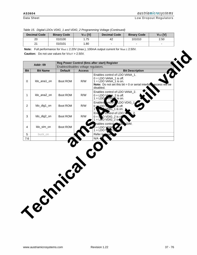
AS3604 aust r iamicrosys temsData Sheet Low Dropout Regu la tors
lid
20 010100 1.75 42 101010 2.5021 010101 1.80 - - -Note: Full performance for Vout ≤ 2.20V (max.), 100mA output current for Vout ≤ 2.50V. Caution: Do not use values for VOUT > 2.50V.
Addr: 09 Reg Power Control (6ms after start) RegisterEnables/disables voltage regulators.
Bit Bit Name Default Access Bit Description
0 ldo_ana1_on Boot ROM R/W
Enables control of LDO VANA_1.0 = LDO VANA_1 is off.1 = LDO VANA_1 is on.Note: Do not set this bit = 0 or serial interface access will be disabled.
1 ldo_ana2_on Boot ROM R/WEnables control of LDO VANA_2. 0 = LDO VANA_2 is off.1 = LDO VANA_2 is on.
2 ldo_dig1_on Boot ROM R/WEnables control of LDO VDIG_1. 0 = LDO VDIG_1 is off.1 = LDO VDIG_1 is on.
3 ldo_dig2_on Boot ROM R/WEnables control of LDO VDIG_2. 0 = LDO VDIG_2 is off.1 = LDO VDIG_2 is on.
4 ldo_sim_on Boot ROM R/WEnables control of LDO VSIM. 0 = LDO VSIM is off. 1 = LDO VSIM is on.
5 buck_on Refer to page 29.7:6 N/A
Table 15. Digital LDOs VDIG_1 and VDIG_2 Programming Voltage (Continued)
Decimal Code Binary Code Vout [V] Decimal Code Binary Code Vout [V]
ams A
G
Technica
l conten
t still
va
www.austriamicrosystems.com Revision 1.22 37 - 76

AS3604 aust r iamicrosys temsData Sheet Low Dropout Regu la tors
lid
Addr: 16 LDO_RF Switch RegisterEnables LDOs as high-side switches.
Bit Bit Name Default Access Bit Description
0 ana1_sw Boot ROM R/W0 = VANA_1 operates as LDO.1 = VANA_1 is operating as high-side switch (Ron = 1Ω); valid
if ldo_rf1_on = 0.
1 ana2_sw Boot ROM R/W0 = VANA_2 operates as LDO.1 = VANA_2 is operating as high-side switch (Ron = 1Ω); valid
if ldo_rf2_on = 0.
2 rf3_sw Boot ROM R/W0 = VRF_3 operates as LDO.1 = LDO VRF_3 is operating as high-side switch (Ron = 2Ω);
valid if ldo_rf3_on = 0.
3 rf4_sw Boot ROM R/W0 = VRF_4 operates as LDO1 = LDO VRF_4 is operating as high-side switch (Ron = 2Ω);
valid if ldo_rf4_on = 0.
4 ldo_rf1_on Boot ROM R/W
Enables control of LDO VRF_1. Set ana1_sw = 0 before setting this bit = 1.0 = LDO VRF_1 is off.1 = LDO VRF_1 is on.
5 ldo_rf2_on Boot ROM R/W
Enables control of LDO VRF_2. Set ana2_sw = 0 before setting this bit = 1.0 = LDO VRF_2 is off.1 = LDO VRF_2 is on.
6 ldo_rf3_on Boot ROM R/W
Enables control of LDO VRF_3. Set rf3_sw = 0 before setting this bit = 1.0 = LDO VRF_3 is off.1 = LDO VRF_3 is on.
7 ldo_rf4_on Boot ROM R/W
Enables control of LDO VRF_4. Set rf4_sw = 0 before setting this bit = 1.0 = LDO VRF_4 is off.1 = LDO VRF_4 is on.
ldo_rfx_on* rfx:sw* RF LDO Function0 0 Off0 1 Fully On, RON = 1 or 2Ω
1 0 Linear Voltage Regulator1 1 Not Allowed
* Where x = 1-4
ams A
G
Technica
l conten
t still
va
www.austriamicrosystems.com Revision 1.22 38 - 76

AS3604 aust r iamicrosys temsData Sheet Low Dropout Regu la tors
lid
Addr: 15 LDO_GPIO Active RegisterActivates GPIO on/off control for voltage regulators.
Bit Bit Name Default Access Bit Description
0 buck_gpio Boot ROM R/W
Activates GPIO control of Step Down DC/DC Converter.0 = Controlled by software. 1 = On when assigned GPIO pin = 1 and bit buck_on (page 29) = 1.
1 ldo_ana2_gpio Boot ROM R/W
Activates GPIO control for LDO VANA_2. 0 = Controlled by software. 1 = On when assigned GPIO pin = 1 and bit ldo_ana2_on (page 37) = 1.
2 ldo_rf1_gpio Boot ROM R/W
Activates GPIO control for LDO VRF_1.0 = Controlled by software. 1 = On when assigned GPIO pin = 1 and bit ldo_rf1_on (page 38) = 1.
3 ldo_rf2_gpio Boot ROM R/W
Activates GPIO control for LDO VRF_2.0 = Controlled by software. 1 = On when assigned GPIO pin = 1 and bit ldo_rf2_on (page 38) = 1.
4 ldo_rf3_gpio Boot ROM R/W
Activates GPIO control for LDO VRF_3.0 = Controlled by software.0 = On when assigned GPIO pin = 1 and bit ldo_rf3_on (page 38) = 1.
5 ldo_rf4_gpio Boot ROM R/W
Activates GPIO control for LDO VRF_4.0 = Controlled by software. 1 = LDO VRF_4 is on when assigned GPIO pin = 1 and bit
ldo_rf4_on (page 38) = 1.
6 ldo_dig1_gpio Boot ROM R/W
Activates GPIO control for LDO VDIG_1.0 = Controlled by software.1 = On when assigned GPIO pin = 1 and bit ldo_dig1_on (page 37) = 1.
7 ldo_dig2_gpio Boot ROM R/W
Activates GPIO control for LDO VDIG_2.0 = Controlled by software.1 = On when assigned GPIO pin = 1 and bit ldo_dig2_on (page 37) = 1.
Addr: 17 LDO_AD GPIO RegisterSelects GPIO pin for power on/off control.
Bit Bit Name Default Access Bit Description
1:0 buck_gpio_sel Boot ROM R/W
Valid if GPIO activation bit buck_gpio (page 39) = 1.00 = GPIO101 = GPIO2 – this setting cannot be selected when GPIO2 is used as feedback pin.10 = GPIO311 = Do not use this setting.
3:2 ldo_ana2_gpio_sel Boot ROM R/W
Valid if GPIO activation bit ldo_ana2_gpio (page 39) = 1.00 = GPIO101 = GPIO210 = GPIO3 11 = Do not use this setting.
5:4 ldo_dig1_gpio_sel Boot ROM R/W
Valid if GPIO-activation bit ldo_dig1_gpio (page 39) = 1.00 = GPIO101 = GPIO2 10 = GPIO3 11 = Do not use this setting.
7:6 ldo_dig2_gpio_sel Boot ROM R/W
Valid if GPIO-activation bit ldo_dig2_gpio (page 39) = 1.00 = GPIO101 = GPIO2 10 = GPIO3 11 = Do not use this setting.
ams A
G
Technica
l conten
t still
va
www.austriamicrosystems.com Revision 1.22 39 - 76

AS3604 aust r iamicrosys temsData Sheet Low Dropout Regu la tors
lid
Addr: 18 LDO_RF GPIO RegisterSelects GPIO pin for power on/off control for RF LDOs VRF_1 - VRF_4.
Bit Bit Name Default Access Bit Description
1:0 ldo_rf1_gpio_sel Boot ROM R/W
Valid if ldo_rf1_gpio (page 39) = 1.00 = GPIO101 = GPIO2 10 = GPIO3 11 = Do not use this setting.
3:2 ldo_rf2_gpio_sel Boot ROM R/W
Valid if ldo_rf2_gpio (page 39) = 1.00 = GPIO101 = GPIO2 10 = GPIO3 11 = Do not use this setting.
5:4 ldo_rf3_gpio_sel Boot ROM R/W
Valid if ldo_rf3_gpio (page 39) = 1.00 = GPIO101 = GPIO2 10 = GPIO3 11 = Do not use this setting.
7:6 ldo_rf4_gpio_sel Boot ROM R/W
Valid if ldo_rf4_gpio (page 39) = 1.00 = GPIO101 = GPIO2 10 = GPIO3 11 = Do not use this setting.
ams A
G
Technica
l conten
t still
va
www.austriamicrosystems.com Revision 1.22 40 - 76

AS3604 aust r iamicrosys temsData Sheet Charge Pump
lid
6.4 Charge PumpThe Charge Pump uses VANA_1 (supplied by Analog LDO VANA_1) as input and doubles this voltage using a flying capacitor between pins CAPP and CAPN (see Figure 1 on page 2) to its output, V5_6. If bit cp_pulseskip (page 41) is set, the Charge Pump compares its output voltage against a voltage reference, defined by cp_vref (page 41), and only starts charging cycles if its output voltage is below cp_vref. If V5_6 is > 5.6V (when VANA_1 is >2.8V), pulseskip will automatically be enabled (depending on bit cp_vref) to protect the pin from overvoltage (bit cp_pulseskip will not be set in this case).
The Charge Pump requires the external components specified in Table 16.
Note: Connections to the two external capacitors should be kept as short as possible.
6.4.1 Charge Pump Control Register
Table 16. Charge Pump External ComponentsSymbol Parameter Min Typ Max Unit Notes
CFLY (C2) External Flying Capacitor 330 nF Ceramic low-ESR capacitor between pins CAPP and CAPN (page 2).
CSTORE (C3) External Storage Capacitor 1 4.7 µF Ceramic low-ESR capacitor between pins V5_6 and VSS (page 2).
Table 17. Charge Pump ParametersSymbol Parameter Min Typ Max Unit NotesICPOUT Output Current 0 30 mA VANA_1 = 2.8V, internal clock selected,
cp_vref (page 41) = 5.25V or cp_pulseskip = 0.VCPOUT Output Voltage 5.0 5.2 5.6 V
VCPOUTI0 Output Voltage (No Load)
2 x VANA_1
VANA_1 ≥ 2.0V, no load at output, cp_pulseskip = 0.
IQUIESCENT Quiescent Current
980
µA
cp_pulseskip = 0, cp_freq (page 41) = 0 (1.1MHz). 498 cp_pulseskip = 0, cp_freq = 1 (550kHz). 5 cp_pulseskip = 1, cp_freq = 0, VANA_1 = 2.8V. 4 cp_pulseskip = 1, cp_freq = 1, VANA_1 = 2.8V.
ISHUTDOWN Shutdown Current 0.1 µA @25ºC VRIPPLE Ripple Voltage 28.8 mVp-p cp_pulseskip = 0, cp_freq = 0, ILOAD = 30mA.
Addr: 24Charge Pump Control RegisterSets the operation mode of the Charge Pump.
Bit Bit Name Default Access Bit Description
0 cp_on Boot ROM R/W0 = Charge Pump is off.1 = Activates the Charge Pump. The Charge Pump is
automatically activated when any of the following blocks are active: Audio Amplifier, VDIG_1, VDIG_2.
1 cp_pulseskip Boot ROM R/W
Controls the Charge Pump pulseskip mode.0 = Always try to double the voltage on VANA_1.1 = Only start a cycle if V5_6 is lower than the voltage defined
by bit cp_vref.
2 cp_vref Boot ROM R/W
If in pulseskip mode, regulate to the following voltage by leaving out complete cycles:0 = 4.74V1 = 5.25V
3 N/A
4 cp_freq Boot ROM R/WSets the Charge Pump clock frequency.0 = System clock1 = System clock/2 (half frequency)
5 onkey_pulldownControls the pulldown on pin ON.0 = Switches on the pulldown on pin ON.1 = Switches off the pulldown on pin ON.
7:6 N/A
ams A
G
Technica
l conten
t still
va
www.austriamicrosystems.com Revision 1.22 41 - 76

AS3604 aust r iamicrosys temsData Sheet Step Up DC/DC Conver ter
lid
6.5 Step Up DC/DC ConverterThe integrated Step Up DC/DC Converter is a high-efficiency current-mode PWM regulator, providing an output volt-age of up to 15V. A constant switching-frequency results in low noise on supply and output voltages. An optional digital NMOS switch is provided for cases when the Step Up DC/DC Converter is not used.
Figure 20. Step Up DC/DC Converter Block Diagram
Table 18. Step Up DC/DC Converter Parameters
Symbol Parameter Min Typ Max Unit NotesVSW High Voltage Pin 0 15 V Pin STEPUP
IVDD_SU Quiescent Current 140 µA Pulse skipping mode
ISHUTDOWN Shutdown Current 100 nA @25ºC
VFB Feedback Voltage, Transient 0 5.5 V Pin CURR1
VFB Feedback Voltage during Regulation 0.65 0.83 1.0 V Pin CURR1
ISW_max Current Limit550 780 1100 mA stpup_on (page 43) = 1
stpup_low_curr (page 43) = 0
350 510 750 mA stpup_on = 1, stpup_low_curr = 1
RSW Switch Resistance 0.85 1.54 Ω stpup_on = 0, stpup_low_curr = 1
ILOAD Load Current 0 45 mA At 15V output voltage.
VPULSESKIP Pulseskip Threshold 1.2 1.33 1.5 V
PIN CURR1. Note: Voltage at pin CURR1, pulse skips are introduced when load current becomes too low.
VRIPPLE Ripple Voltage 146 mVp-p stpup_freq (page 43) = 0, VOUT = 15V, ILOAD = 45mA, BW ≤ 20MHz.
fIN Fixed Switching Frequency1 1.1 1.2
MHz1.1MHz; stpup_freq = 0
0.5 0.55 0.6 0.55MHz; stpup_freq = 1
COUT Output Capacitor 1 µF Ceramic
L (Inductor)ILOAD > 20mA 17 22 27
µHUse inductors with small CPARASITIC (<100pF) for high efficiency.ILOAD < 20mA 8 10 27
tMIN_ON Minimum On-Time 90 180 ns
MDC Maximum Duty Cycle 88 91 94 % Guaranteed per design.
+
CLK
S
–
CURR1
STEPUP
PWMLogic
SW_ON
VSS
VBAT5
+-
1.33V
0.83V
NMOS 15VPower Device0.85Ω (typ.)
Pulse SkipComparator
ErrorAmplifier
RampGeneration
Comparator
+-
CurrentSense
VBAT
RLOAD
L122µH
1µF
Driver
ams A
G
Technica
l conten
t still
va
www.austriamicrosystems.com Revision 1.22 42 - 76

AS3604 aust r iamicrosys temsData Sheet Step Up DC/DC Conver ter
lid
6.5.1 Step Up DC/DC Converter Register
Figure 21. Typical Performance Characteristics
Addr: 25 Step Up DC/DC Converter Control RegisterSets the operation mode of the Step Up DC/DC Converter.
Bit Bit Name Default Access Bit Description
0 stpup_on Boot ROM R/WActivates the Step Up DC/DC Converter.0 = Step Up DC/DC Converter is off.1 = Step Up DC/DC Converter is on.
1 stpup_sw_on Boot ROM R/W
This bit controls the NMOS switch on pin STEPUP only if stpup_on = 0.0 = Switch open (STEPUP floating).1 = Switch closed (STEPUP pulled to VSS).
2 stpup_freq Boot ROM R/WDefines the clock frequency of the Step Up DC/DC Converter.0 = System clock (typ. 1.1MHZ).1 = System clock/2 (half frequency).
3 stpup_low_curr Boot ROM R/WNMOS-switch current-limit control only if stpup_on = 1.0 = High current limit (600mA).1 = Low current limit (300mA).
7:4 N/A
Efficiency 15V DCDC
60.000
65.000
70.000
75.000
80.000
85.000
90.000
1.000 10.000 100.000
Output Current [mA]
Effic
ienc
y [%
] 22uH / WE-PD3 / 1.1 MHz
22uH / WE-PD3 / 550kHz
22uH / DO1608C / 1.1MHz
22uH / DO 1608C / 550kHz
10uH / DO 1608C / 1.1MHz10uH / DO1608C / 550kHz
ams A
G
Technica
l conten
t still
va
www.austriamicrosystems.com Revision 1.22 43 - 76

AS3604 aust r iamicrosys temsData Sheet Genera l Purpose Input /Output
lid
6.6 General Purpose Input/Output The general purpose input/output pins (GPIO1 - GPIO3) are highly configurable and independently controlled.
GPIO1 - GPIO3 can be used to accommodate the following functionality:
Software controlled input and outputInput pin for the WatchdogSignal input (GPIO1-GPIO3) Interrupt output with configurable interrupt sourceConfigurable frequency and duty cycle outputExternal clock input for Step Up/Down DC/DC Converters and Charge Pump synchronization (GPIO1 only)Active pullup or pulldown; can be combined with other I/O functionsOutput open drain (push or pull type)Output high-level voltage selection between V5_6 or VANA_1; (V5_6 not possible on GPIO2)Optional feedback input for Step Down DC/DC Converter (GPIO2)
Table 19. DC Characteristics Input/Output Pin with Selectable Supply GPIO1:GPIO3 Parameter Symbol Min Max Unit Notes
High-Level Input Voltage VIH 0.7 x VANA_1 VLow-Level Input Voltage VIL 0.3 x VANA_1 V
Hysteresis VHYS 0.2 x VANA_1 VInput Leakage Current
(if not used as pulldown/pullup) ILEAK -5 5 µA to VANA_1 and VSS
Pulldown Current(if configured as pulldown) IPULLDOWN 5 50 µA to VSS
Pullup Current(if configured as pullup) IPULLUP -200 -20 µA
to V5_6 or VANA_1 as configured
High-Level Output VoltageSupply VANA_1 VOH 0.8 x VANA_1 V at -2mA
High-Level Output VoltageSupply V5_6 (V5_6 min. 5.0V) VOHHV 0.8 x V5_6 V at -2mA
Low-Level Output Voltage VOL 0.2 x VANA_1 V at 2mACapacitive Load CLOAD 50 pF
ams A
G
Technica
l conten
t still
va
www.austriamicrosystems.com Revision 1.22 44 - 76

AS3604 aust r iamicrosys temsData Sheet Genera l Purpose Input /Output
lid
Figure 22. General Purpose I/O Block Diagram
6.6.1 GPIO RegistersGPIO1 - GPIO3 are controlled by the registers listed in Table 20.
Table 20. GPIO Register Summary
Name Addr B7 B6 B5 B4 B3 B2 B1 B0 Page
GPIO1 Control Register 26 gpio1_out_src gpio1_invert gpio1_pulls gpio1_
voltage gpio1_mode 46
GPIO2 Control Register 27 gpio2_out_src gpio2_invert gpio2_pulls stepdown
_fb gpio2_mode 46
GPIO3 Control Register 28 gpio3_out_src gpio3_invert gpio3_pulls gpio3_
voltage gpio3_mode 47
GPIO Signal Register 33 N/A gpio3 gpio2 gpio1 47GPIO Frequency Control High Time Register 34 gpio_h_time 48
GPIO Frequency Control Low Time Register 35 gpio_l_time 48
Clock Generation Register 30 N/A ext_clk 48
Interrupt Enable Register 31 chgov_int_en
chgrmv_int_en
resume_int_en
chdet_int_en
onkey_int_en
ovtmp_int_en
vchoff_int_en
wdog_int_en 49
Interrupt Status Register 32 chgov_i chgrmv_i resume_i chdet_i onkey_i ovtmp_i vchoff_i wdog_i 49
GPIOx
RegisterGPIO
Control
FrequencyGenerator
Interrupt
MUX
Interrupt Sources
int
f_out
gpio
gpio_out_srcgpio_inverten_nmosen_pmos
en_pupgpio_v
en_pdwn
sysclk
interface
VANA_1 V5_6
VANA_1
ams A
G
Technica
l conten
t still
va
www.austriamicrosystems.com Revision 1.22 45 - 76

AS3604 aust r iamicrosys temsData Sheet Genera l Purpose Input /Output
lid
Addr: 26 GPIO1 Control RegisterConfigures pin GPIO1.
Bit Bit Name Default Access Bit Description
1:0 gpio1_mode Boot ROM R/W
Sets the direction for pin GPIO1. 00 = Input only.01 = Output (push and pull).10 = Output (open drain, only push; only NMOS is active).11 = Output (open drain, only pull; only PMOS is active).
2 gpio1_voltage Boot ROM R/W
If pin GPIO1 is used as output, sets the positive supply (GND_PAD is always used as negative supply).0 = VANA_11 = V5_6
4:3 gpio1_pulls Boot ROM R/W
Sets pullup/pulldown to pin GPIO1 (independent of bit gpio1_mode setting).00 = None01 = Pulldown10 = Pullup11 = N/A
5 gpio1_invert Boot ROM R/W
0 = Output signal is not inverted.1 = Inverts any output signal going to GPIO1. This is useful for
the Watchdog output source to make the output active high or low.
7:6 gpio1_out_src Boot ROM R/W
Sets the source of pin GPIO1 output.x0 = Bit gpio1 (page 47) controlled through the serial interface.01 = Frequency generator defined by bits gpio_h_time (page
48) and gpio_l_time (page 48).11= Interrupt signal (see Interrupt Function on page 49).
Addr: 27 GPIO2 Control RegisterConfigures pin GPIO2.
Bit Bit Name Default Access Bit Description
1:0 gpio2_mode Boot ROM R/W
Sets the direction for pin GPIO2.00 = Input only.01 = Output (push and pull).10 = Output (open drain, only push; only NMOS is active).11 = Output (open drain, only pull; only PMOS is active).
2 stepdown_fb Boot ROM R/W
0 = GPIO2 is used as regulator configurable I/O pin, Step Down DC/DC Converter feedback is at pin VBUCK.
1 = Pin GPIO2 is used as feedback-pin for Step Down DC/DC Converter.
4:3 gpio2_pulls Boot ROM R/W
Sets pullup/pulldown to pin GPIO2 (independent of bit gpio2_mode setting).00 = None 10 = Pullup01 = Pulldown 11 = N/A
5 gpio2_invert Boot ROM R/W
0 = Output signal is not inverted.1 = Inverts any output signal going to pin GPIO2. This is useful
for the Watchdog output source to make the output active high or low.
7:6 gpio2_out_src Boot ROM R/W
Sets the source of pin GPIO2 output.x0 = Bit gpio2 (page 47) (controlled through the serial interface).01 = Frequency generator defined by bits gpio_h_time (page 48)
and gpio_l_time (page 48).11= Interrupt signal (see Interrupt Function on page 49).
ams A
G
Technica
l conten
t still
va
www.austriamicrosystems.com Revision 1.22 46 - 76

AS3604 aust r iamicrosys temsData Sheet Genera l Purpose Input /Output
lid
6.6.2 Programmable Frequency GeneratorThe Programmable Frequency Generator is controlled by bits gpio_h_time (page 48) and gpio_l_time (page 48). It gener-ates a waveform with 0.9 microseconds times gpio_h_time high-level and 0.9 microseconds times gpio_l_time low-level. The accuracy of these timings is ±10%.
The frequency of the Programmable Frequency Generator is:
f=1/(tCLK*gpio_h_time + tCLK*gpio_l_time) (EQ 8)
where tclk = 1/fCLK (page 17) = 1/1.1MHz (typ.) = 0.909µs (typ.)
The purpose of the Programmable Frequency Generator is to have a controlled sweepable frequency or duty cycle source for one of the following:
General User-Defined Clock8-Bit DAC (output should be filtered by an RC filter)(High) Positive and Negative Voltage Generation (see 25V/-20V Voltage Generator on page 48)
Addr: 28 GPIO3 Control RegisterConfigures pin GPIO3.
Bit Bit Name Default Access Bit Description
1:0 gpio3_mode Boot ROM R/W
Sets the direction for pin GPIO3.00 = Input only.01 = Output (push and pull).10 = Output (open drain, only push; only NMOS is active).11 = Output (open drain, only pull; only PMOS is active).
3:2 gpio3_voltage Boot ROM R/W
If pin GPIO1 is used as output, sets the positive supply (GND_PAD is always used as negative supply).0 = VANA_11 = V5_6
gpio3_pulls Boot ROM R/W
Sets pullup/pulldown to pin GPIO3 (independent of bit gpio3_mode setting).00 = None 10 = Pullup01 = Pulldown 11 = N/A
4
5 gpio3_invert Boot ROM R/W
0 = Output signal is not inverted.1 = Inverts any output signal going to pin GPIO3. This is useful
for the Watchdog output source to make the output active high or low.
7:6 gpio3_out_src Boot ROM R/W
Sets the source of pin GPIO3.x0 = Bit gpio3 (page 47) (controlled through the serial interface)01 = Frequency generator defined by bits gpio_h_time (page 48)
and gpio_l_time (page 48).11 = Interrupt signal (see Interrupt Function on page 49).
Addr: 33 GPIO Signal RegisterReads the logic signal of the GPIO pins, independently of any other GPIO bit setting.
Bit Bit Name Default Access Bit Description
0 gpio1 N/A R/W Reads the logic signal from pin GPIO1. If gpio1_out_src (page 46) = 00, this is the output signal at pin GPIO1.
1 gpio2 N/A R/W Reads the logic signal from pin GPIO2. If gpio2_out_src (page 46) = 00, this is the output signal at pin GPIO2.
2 gpio3 N/A R/W Reads the logic signal from pin GPIO3. If gpio3_out_src (page 47) = 00, this is the output signal at pin GPIO3.
7:3 N/A
ams A
G
Technica
l conten
t still
va
www.austriamicrosystems.com Revision 1.22 47 - 76

AS3604 aust r iamicrosys temsData Sheet Genera l Purpose Input /Output
lid
6.6.3 Programmable Frequency Generator Registers
6.6.4 25V/-20V Voltage GeneratorUsing the Programmable Frequency Generator a voltage generator for +25V or -20V can be built with only 4 external capacitors and 5 external Shottky diodes as shown in the following diagrams.
Figure 23. 25V Positive Voltage Generator Block Diagram
Figure 24. -20V Voltage Generator Block Diagram
Note: GPIO2 and GPIO3 must be 180º out of phase, e.g., set bit gpio2_invert (page 46) = 1 and bit gpio3_invert (page 47) = 0.
Addr: 34 GPIO Frequency Control High Time RegisterConfigures programmable frequency generator.
Bit Bit Name Default Access Bit Description
7:0 gpio_h_time 64h R/W
Defines the number of system clock cycles (typ. 0.9µs), that the programmable frequency generator at the GPIO output(s) is high.00h = 0.909µsFFh = 232.7µs
Addr: 35 GPIO Frequency Control Low Time RegisterConfigures programmable frequency generator.
Bit Bit Name Default Access Bit Description
7:0 gpio_l_time 64h R/W
Defines the number of system clock cycles (typ. 0.9µs), that the programmable frequency generator at the GPIO output(s) is low.00h = 0.909µsFFh = 232.7µs
Addr: 30 Clock Generation RegisterSets the source for the system clock.
Bit Bit Name Default Access Bit Description
0 ext_clk Boot ROM R/W 0 = Internal 1.1MHz RC-oscillator.1 = System clock controlled by pin GPIO1.
7:1 N/A
GPIO3V5_6 GPIO2
+25V
100nF100nF100nF100nF
GPIO3
-20V
GNDGPIO2
100nF 100nF 100nF 100nF
ams A
G
Technica
l conten
t still
va
www.austriamicrosystems.com Revision 1.22 48 - 76

AS3604 aust r iamicrosys temsData Sheet Genera l Purpose Input /Output
lid
6.6.5 Interrupt FunctionAny of the GPIO pins (GPIO1 - GPIO3) can be configured as interrupt output pins. To enable this function, the corre-sponding GPIO control bits must be set to 11b. See gpio1_out_src (page 46), gpio2_out_src (page 46), or gpio3_out_src (page 47).
Several signals can be configured as interrupt source using the Interrupt Enable Register. A rising edge of an enabled interrupt control signal sets the selected GPIO interrupt output pin = 1.
The Interrupt Status Register shows the currently active interrupt signals. Reading this register resets the Interrupt Sta-tus Register bits and sets the active GPIO pin (GPIO 1 - GPIO3) = 0.
6.6.6 Interrupt Registers
Addr: 31 Interrupt Enable RegisterEnables/disables interrupt sources.
Bit Bit Name Default Access Bit Description
0 wdog_int_en Boot ROM R/W0 = Disables watchdog alarm as interrupt source signal.1 = Enables watchdog alarm as interrupt source signal.
1 vchoff_int_en Boot ROM R/W
0 = Disables charge termination voltage as interrupt source signal.
1 = Enables charge termination voltage as interrupt source signal.
2 ovtmp_int_en Boot ROM R/W0 = Disables ov_temp_110 (device temperature alert at 110ºC).1 = Enables ov_temp_110 (device temperature alert at 110ºC).
3 onkey_int_en Boot ROM R/W0 = Disables pin ON (active high). 1 = Enables pin ON (active high).
4 chdet_int_en Boot ROM R/W0 = Disables charger detection.1 = Enables charger detection.
5 resume_int_en Boot ROM R/W0 = Disables charger-resume interrupt.1 = Enables charger-resume interrupt.
6 chgrmv_int_en Boot ROM R/W0 = Disables charger-removed interrupt.1 = Enables charger-removed interrupt.
7 chgov_int_en Boot ROM R/W0 = Disables charger overvoltage interrupt.1 = Enables charger overvoltage interrupt.
Addr: 32 Interrupt Status RegisterDisplays the status of the interrupt inputs.
Bit Bit Name Default Access Bit Description
0 wdog_i Boot ROM R/W 0 = Software or hardware watchdog is off or has not rolled over.1 = Software or hardware watchdog is rollover.
1 vchoff_i Boot ROM R/W0 = Battery voltage is below VCHOFF (page 8) threshold.1 = Battery voltage has reached VCHOFF threshold.
2 ovtmp_i Boot ROM R/W0 = Device temperature is below 110ºC.1 = 110ºC temperature threshold ov_temp_110 (page 59) has
been reached.
3 onkey_i Boot ROM R/W0 = ON key has not been pressed.1 = ON key has been pressed (rising edge).
4 chdet_i Boot ROM R/W Charger detection interrupt, active if chDet (page 19) is falling.5 resume_i Boot ROM R/W Resume charging interrupt, active if Bat_v (page 21) is falling.6 chgrmv_i Boot ROM R/W Charger detection interrupt, active if chDet (page 19) is falling.7 chgov_i Boot ROM R/W Charger over voltage interrupt, active if ChOv (page 21) is rising.
ams A
G
Technica
l conten
t still
va
www.austriamicrosystems.com Revision 1.22 49 - 76

AS3604 aust r iamicrosys temsData Sheet Cur rent S inks
lid
6.7 Current SinksThe AS3604 contains general purpose current sinks intended to control backlights, buzzers, and vibrators. All current sinks have an integrated protection (VPROTECT) against overvoltage and can therefore also drive inductive loads. CURR1 is also used as feedback for Step Up DC/DC Converter and in this configuration regulated to 0.8V.
The current sinks can also be used as switches to VSS with configurable impedance as indicated in Table 21.
Note: If a voltage higher than VPROTECT is applied to pins CURR1 - CURR4, a current of more than 20mA will flow into the AS3604. This protects the device from voltage rises caused by inductive loads.
6.7.1 Current Sink RegistersThe current sinks are controlled by the registers listed in Table 22.
Table 21. Current Source Characteristics
Symbol Parameter Min Typ Max Unit Notes
ICURRx currx_current = 01h - FFh 0.625 160 mA currx_sw = 0,resolution = 0.625mA
RPD_SW currx_current = 01h - FFh 0.3 77 Ω currx_sw = 1, 00h = open,resolution = 0.3Ω
VPROTECTMaximum voltage at pin CURRx to protect driver
transistorVBAT + 2.0V V ISINK ≥ 20mA (1)
Table 22. Current Sink Register Summary
Name Addr B7 B6 B5 B4 B3 B2 B1 B0 PageCURR1 Value Register 36 curr1_current 50CURR2 Value Register 37 curr2_current 50CURR3 Value Register 38 curr3_current 51CURR4 Value Register 39 curr4_current 51CURR Control Register 40 curr4_ctrl curr3_ctrl curr2_ctrl curr1_ctrl 51CURR Mode Register 41 N/A curr4_sw curr3_sw curr2_sw curr1_sw 51CURR GPIO Map Register 42 curr4_gpio curr3_gpio curr2_gpio curr1_gpio 52
Addr: 36 CURR1 Value RegisterSets the current / resistance of current source CURR1.
Bit Bit Name Default Access Bit Description
7:0 curr1_current 00h R/W00h01h…FFh
curr1_sw (page 51) = 0 Power Down 0.625mA…160mA
curr1_sw = 1Open77Ω…0.3Ω
Addr: 37 CURR2 Value RegisterSets the current / resistance of current source CURR2.
Bit Bit Name Default Access Bit Description
7:0 curr2_current 00h R/W00h01h…FFh
curr2_sw (page 51) = 0 Power Down 0.625mA…160mA
curr2_sw = 1Open77Ω…0.3Ω
ams A
G
Technica
l conten
t still
va
www.austriamicrosystems.com Revision 1.22 50 - 76

AS3604 aust r iamicrosys temsData Sheet Cur rent S inks
lid
Addr: 38 CURR3 Value RegisterSets the current / resistance of current source CURR3.
Bit Bit Name Default Access Bit Description
7:0 curr3_current 00h R/W00h01h…FFh
curr3_sw (page 51) = 0 Power Down 0.625mA…160mA
curr3_sw = 1Open77Ω…0.3Ω
Addr: 39 CURR4 Value RegisterSets the current / resistance of current source CURR4.
Bit Bit Name Default Access Bit Description
7:0 curr4_current 00h R/W00h01h…FFh
curr4_sw (page 51) = 0 Power Down 0.625mA…160mA
curr4_sw = 1Open77Ω…0.3Ω
Addr: 40 CURR Control RegisterSelects software/ hardware control of current sources.
Bit Bit Name Default Access Bit Description
1:0 curr1_ctrl 00b R/W00 = Pin CURR2 is turned off.01 = Pin CURR2 is active.1x = GPIO control; pin is active when curr1_gpio (page 52) =1.
3:2 curr2_ctrl 00b R/W00 = Pin CURR2 is turned off.01 = Pin CURR2 is active.1x = GPIO control; pin is active when curr2_gpio (page 52) =1.
5:4 curr3_ctrl 00b R/W00 = Pin CURR4 is turned off.01 = Pin CURR4 is active.1x = GPIO control; pin is active when curr3_gpio (page 52) = 1.
7:6 curr4_ctrl 00b R/W00 = Pin CURR4 is turned off.01 = Pin CURR4 is active.1x = GPIO control; pin is active when curr4_gpio (page 52) = 1.
Addr: 41 CURR Mode RegisterSelects operation mode for current sources.
Bit Bit Name Default Access Bit Description
0 curr1_sw R/W0 = Pin CURR1 is operating as current sink.1 = Pin CURR1 is operating as resistive load current.
Resistance is defined by bits curr1_current (page 50).
1 curr2_sw R/W0 = Pin CURR2 is operating as current sink.1 = Pin CURR2 is operating as resistive load current.
Resistance is defined by bits curr2_current (page 50).
2 curr3_sw R/W0 = Pin CURR3 is operating as current sink.1 = Pin CURR3 is operating as resistive load current.
Resistance is defined by bits curr3_current (page 51).
3 curr4_sw R/W0 = Pin CURR4 is operating as current sink.1 = Pin CURR4 is operating as resistive load. Resistance is
defined by bits curr4_current (page 51).7:4 N/A
ams A
G
Technica
l conten
t still
va
www.austriamicrosystems.com Revision 1.22 51 - 76

AS3604 aust r iamicrosys temsData Sheet Cur rent S inks
lid
Addr: 42 CURR GPIO Map RegisterSelects GPIO pin to control current sources.
Bit Bit Name Default Access Bit Description
1:0 curr1_gpio Boot ROM R/W
If bits curr1_ctrl (page 51) = 1x, the following pin is assigned for turning the CURR1 pin on and off.00 = GPIO101 = GPIO2 10 = GPIO3
3:2 curr2_gpio Boot ROM R/W
If bits curr2_ctrl (page 51) = 1x, the following pin is assigned for turning the CURR2 pin on and off.00 = GPIO101 = GPIO2 10 = GPIO3
5:4 curr3_gpio Boot ROM R/W
If bits curr3_ctrl (page 51) = 1x, the following pin is assigned for turning the CURR3 pin on and off.00 = GPIO101 = GPIO2 10 = GPIO3
7:6 curr4_gpio Boot ROM R/W
If bits curr4_ctrl (page 51) = 1x, the following pin is assigned for turning the CURR4 pin on and off.00 = GPIO101 = GPIO2 10 = GPIO3
ams A
G
Technica
l conten
t still
va
www.austriamicrosystems.com Revision 1.22 52 - 76

AS3604 aust r iamicrosys temsData Sheet Aud io Ampl i f i e r
lid
6.8 Audio AmplifierThe integrated Audio Amplifier provides real CD-quality audio and can be used as a headphone amplifier for portable devices. It is designed to meet the operational and power requirements of portable devices by delivering:
1WRMS continuous power into 8Ω differential at 5V supply2 x 50mWRMS into 32Ω single-ended at 5V supply
The Audio Amplifier provides the following operational features:
Total harmonic distortion is less than 0.1% at 1kHz and the quiescent current does not exceed 8mA.Power supply rejection is always better than 50dB and allows direct connection to noisy batteries, e.g. in TDMA systems. The internal programmable gain can be used for volume and balance control. Only a few external components are required for AC-coupling and reference bypass. An internal smooth-rampup circuit ensures pop- and click-less startup without expensive and bulky external relays.Device stability even with high capacitive loads of 1nF and does not require external snubber networks.Inputs are high-impedance in power-down.
Figure 25. Audio Amplifier Block Diagram – Stereo Mode
Note: The value of the audio output decoupling capacitors depends on the speaker impedance and the desired mini-mum output frequency:
C = 1/(2xPxfxR) (EQ 9)
Where:f = minimum output cutoff frequency, -3dB point.R = speaker impedance in Ω.C = decoupling capacitance in F.
+
–Startup, Biasing, Control Logic
AOUT_R–
+
AOUT_LGain Control
AIN_R
AIN_L
aud_gain <4:0>
AGND
aud_on
aud_lpo
100nF
100nF
100nF ≥4Ω
≥4Ω
≥100µF
≥100µF
330kΩ
Audio In Left
Audio In Right
Bit aud_stereo (page 55) = 1
330kΩ
ams A
G
Technica
l conten
t still
va
www.austriamicrosystems.com Revision 1.22 53 - 76

AS3604 aust r iamicrosys temsData Sheet Aud io Ampl i f i e r
lid
Figure 26. Audio Amplifier Block Diagram – Differential Mode
Table 23. Audio Amplifier Characteristics
Symbol Parameter Min Typ Max Unit Notes
VDDH Supply Voltage Range (VBAT_3) 3 5.5 V
PSRR Power Supply Rejection Ratio, Differential
70dB
f = 1kHz
50 f = 20kHz
PSRR Power Supply Rejection Ratio, Single-Ended
50dB
f = 1kHz
40 f = 20kHz
IOFF Shut Down Current 100 nA
IVDDH Supply Current (Differential Mode)
9
mA
aud_lpo (page 55) = 0 and aud_ib_red (page 55) = 00
4 aud_lpo = 1 and aud_ib_red = 00
2.7 aud_lpo = 1 and aud_ib_red = 11
IVDDH Supply Current (Stereo Mode)
8
mA
aud_lpo = 0 and aud_ib_red = 00
3 aud_lpo = 1 and aud_ib_red = 00
1.7 aud_lpo = 1 and aud_ib_red = 11
RLOAD Output Load8
ΩDifferential mode
4 Stereo mode
THD+N Total Harmonic Distortion
0.1 % POUT = 1W, RLOAD = 8Ω, f = 1kHz Differential
0.5 % POUT = 1W, RLOAD = 8Ω, f = 20kHz Differential
0.05 % POUT = 50mW, RLOAD =32Ω, f = 1kHz Single-Ended
0.2 % POUT = 50mW, RLOAD =32Ω, f = 20kHz Single-Ended
SNR Signal to Noise Ratio 84 91 dB VBAT=3.7V, not tested, guaranteed per design
A0 Gain -22 0 20 dB Programmable gain: AOUT/AIN
ΔAx Programmable Gain Step-Size 3 dB
lOV_ON Overcurrent On_limit 591 650 744 mA Current rising into PMOS driver; when aud_lpo = 0 and aud_ib_red = 00, and aud_overcur = 1 .
+
–Startup, Biasing, Control Logic
AOUT_R–
+
AOUT_L
AIN_R
aud_gain <4:0>
AGND
aud_on
aud_lpo
100nF
100nF
≥8Ω
Gain Control
Audio InAIN_L
100nF
165kΩ 165kΩ
330kΩ
Bit aud_stereo (page 55) = 0
ams A
G
Technica
l conten
t still
va
www.austriamicrosystems.com Revision 1.22 54 - 76

AS3604 aust r iamicrosys temsData Sheet Aud io Ampl i f i e r
lid
6.8.1 Audio Amplifier Registerslov_off Overcurrent Off_limit 397 550 650 mACurrent decreasing in PMOS driver; when aud_lpo = 0 and aud_ib_red = 00, and aud_overcur (page 55) is cleared.
lov_hyst Overcurrent Hysteresis 100 mA
Addr: 43 Audio Control RegisterConfigures the Audio Amplifier.
Bit Bit Name Default Access Bit Description
0 aud_on 0 R/W
Activates the Audio Amplifier.0 = Audio amplifier off; inputs AIN_L and AIN_R are high-
impedance.1 = Audio amplifier on.
1 aud_lpo 0 R/W
Select Low-Power Operation; reduced output power.0 = Use for speakers < 32Ω (nominal impedance) in stereo
mode; < 64Ω differential. 1 = Use for speakers ≥ 32Ω (nominal impedance) in stereo
mode; ≥ 64Ω differential.
3:2 aud_ib_red 00b R/W
Reduced bias current into Audio Amplifier circuit.00 = Use for speakers < 8Ω (nominal impedance) in stereo mode; < 16Ω differential.01 = N/A10 = N/A11 = Use for speakers ≥ 8Ω (nominal impedance) in stereo mode; ≥ 16Ω differential.
7:4 aud_gain 0000b R/W
Audio Amplifier gain adjust.0000 = Output off 1000 = 0dB0001 = -22dB 1001 = +2dB0010 = -19dB 1010 = +5dB0011 = -16dB 1011 = +8dB0100 = -13dB 1100 = +11dB0101 = -10dB 1101 = +14dB0110 = -7dB 1110 = +17dB0111 = -4dB 1111 = +20dB
Addr: 65 Audio Control 2 RegisterConfigures the Audio Amplifier.
Bit Bit Name Default Access Bit Description
0 aud_stereo 1 R/WSelects audio mode.0 = Differential mono mode (connect pin AIN_R to pin AOUT_L)1 = Stereo mode.
1 aud_overcur 00 R0 = Normal operation; audio output current below limit of
lOV_ON (page 54).1 = Audio output current exceeds limit (lOV_ON).
3:2 aud_pulldwn 00b R/W
Audio amplifier output pulldown control; active if aud_on (page 55)=0.00 = 30µA 01 = 0.6mA10 = 1.2mA11 = 2.5mA
7:4 N/A
Table 23. Audio Amplifier Characteristics (Continued)
Symbol Parameter Min Typ Max Unit Notes
ams A
G
Technica
l conten
t still
va
www.austriamicrosystems.com Revision 1.22 55 - 76

AS3604 aust r iamicrosys temsData Sheet Reset
lid
7 System Supervisory Functions7.1 ResetRESET is an active low bi-directional pin; an external pullup to LDO VANA_1 has to be added (see Digital Input/Output DC/AC Characteristics on page 64). During each reset cycle the following states are controlled by the AS3604:
Pin RESET is Forced to GNDProgrammable Power-off FunctionProgrammable Power-on Sequence and Regulator VoltagesProgrammable Reset TimerAll Register bits Set to Default Values after Power-On (except the Audio Control 2 Register (page 55), the Interrupt Status Register (page 49), and the Boot Sequence Detection Register (page 63).
Note: Programming is controlled by the internal mask-ROM and the external resistor RPROGRAM. The first address of each ROM-bank defines which of the regulators are turned off during reset.
7.1.1 Reset ConditionsReset can be activated from 7 different sources:
Power On (Battery or Charger Insertion)Low BatteryPower Off ModeSoftware Forced ResetExternally Triggered through the RESET PinOvertemperatureWatchdogMomentary Power Loss Detection
Power On (Battery or Charger Insertion)There are two types of voltage dependent resets:
VPOR – Monitors the voltage on pin V2_5. LDO V2_5 uses the voltage VCHARGER or VBAT as its source.VRESET – Monitors the voltage on VBAT pins. Pin RESET is only released if V2_5 >VPOR and VBAT > VRESETRISE.
Low BatteryA reset is automatically generated if VBAT drops below VRESETFALLING for a minimum period (VRESETMASk). Table 24. Reset Levels
Symbol Parameter Min Typ Max Unit Notes
VPOR Overall power on reset 1.5 2.0 2.3 V
Monitor voltage on pin V2_5; power on reset for all internal functions. Note: Pin RESET stays low until V2_5 >
VPOR
VRESETRISE Reset level for VBAT rising 3.1 V Monitor voltage on pin VBAT; rising level.
VRESETFALLING Reset level for VBAT falling 1
1. VRESETFALLING is only accepted if the reset condition is longer than VRESETMASK. This guard time is used to avoid a complete reset of the system in case of short drops of VBAT.
2.8 V Monitor voltage on pin VBAT; falling level.
VRESETMASK Mask time for VRESETFALLING 40 µs Duration for VBAT < VRESETFALLING until a
reset cycle is started. 2
2. VRESET signal is debounced with the specified mask time for rising- and falling-slope of VBAT. The default time is 40µs and it can be programmed from 0µs to 200µs with the register reset-mask timer.
Momentary Power Loss DetectionIf the battery voltage (VBAT) drops below VRESETFALLING and rises above VRESETRISE within TPOWERLOSS, the AS3604 automatically restarts and sets bit tmp_ pwr_loss (page 57) to 1. This can be used to detect short VBAT interruptions, e.g., due to a dropped mobile phone call.
TPOWERLOSS Interval for recovery of power loss on VBAT 100 250 500 ms If the duration of a power loss on VBAT is
below this duration, the system will restart
ams A
G
Technica
l conten
t still
va
www.austriamicrosystems.com Revision 1.22 56 - 76

AS3604 aust r iamicrosys temsData Sheet Reset
lid
Power OffSetting bit power_off (page 57) = 1 puts the AS3604 into ultra low-power mode. To start a complete reset cycle, the AS3604 waits until the external pin ON is pulled high, the Battery Charger is inserted, or level VPOR is reached. Bit power_off is automatically cleared by this reset cycle. During power off state, all circuits are turned off except LDO V2_5, thus the current consumption of the AS3604 is reduced to less than 10µA. The digital part is supplied by LDO V2_5, all other circuits are turned off in this mode, including internal references and oscillator. Note: All registers except the Reset Control Register (page 57) are set to their default value after power-on.Software Forced ResetSetting bit force_reset (page 57) = 1 immediately initiates a reset cycle, and is automatically cleared during a reset.External Triggered ResetIf the pin RESET is pulled from high to low by an external source (microprocessor or button) a reset cycle is initiated.Overtemperature ResetThe reset cycle can be started by overtemperature conditions (page 59).Watchdog ResetIf the Watchdog is armed (bit wtdg_on (page 60) = 1 and bit wtdg_res_on (page 60) = 1) and the timer expires, a reset is initiated. Refer to page 60 for information about the Watchdog block.
7.1.2 Reset Registers
Addr: 58 Reset Control RegisterControls reset and power off.
Bit Bit Name Default Access Bit Description
0 force_reset 0b R/W0 = Normal operation.1 = Initiates a complete reset cycle.
1 power_off 0b R/W
0 = Normal operation.1 = Initiates power-off mode where all LDOs are turned off except LDO
V2_5. The AS3604 waits for a rising edge on pin ON or until the battery charger is detected.
2 on_input N/A RStatic indication of ON input pin.0 = ON input pin is low.1 = ON input pin is high (external ON key depressed).
5:3 reset_reason N/A R
Indicates to the software the reason for the most recent reset.000 = VPOR (page 56) was reached (initial battery or charger insertion).001 = VRESETFALLING (page 56) was reached (VBAT < 2.75V).010 = Software forced by bit force_reset.011 = Software forced by bit power_off and ON was pulled high.100 = Software forced by bit power_off and a Battery Charger detected.101 = Externally triggered through pin RESET.110 = Reset caused by overtemperature T140.111 = Reset caused by Watchdog.
6 tmp_ pwr_loss 0b R0 = Normal startup.1 = A momentary power loss condition was detected.
7 N/A
Addr: 19 Reset Timer RegisterSets the RESET timer value.
Bit Bit Name Default Access Bit Description
2:0 res_timer Boot ROM R/W
Set RESTIME
000 RESTIME = 10ms 100 RESTIME = 50ms001 RESTIME = 20ms 101 RESTIME = 60ms010 RESTIME = 30ms 110 RESTIME = 70ms011 RESTIME = 40ms 111 RESTIME = 80ms
5:3 reset_mask_timer 11b R/W
Set MASKTIME
000 = MASKTIME = 0µs 100 MASKTIME = 80µs001 MASKTIME = 5µs 101 MASKTIME = 120µs010 MASKTIME = 10µs 110 MASKTIME = 160µs011 MASKTIME = 40µs 111 MASKTIME = 200µs
7:5 N/A
ams A
G
Technica
l conten
t still
va
www.austriamicrosystems.com Revision 1.22 57 - 76

AS3604 aust r iamicrosys temsData Sheet Star tup
lid
7.1.3 Reset CycleDuring a reset cycle, pin RESET is forced low for at least the time specified by bits res_timer (page 57) and then all reg-ister bits are set to their default values except bit ov_temp_140 (page 59) and the Boot Sequence Detection Register (page 63).
During the reset time, a normal startup is initiated (refer to Startup on page 58) and the reset is active until the reset timer (set by bits res_timer) expires. The voltage on pin RESET is then pulled high by the external resistor and the whole system is leaving the reset state.
7.1.4 res_con: Reset ControlReset is internally generated from a power on detection circuit (page 56) and provided to the internal logic as well as externally through the open-drain pin RESET. This pin can also be forced externally by pulling it low. Additionally Reset can be forced by software by setting bit force_reset (page 57) = 1.
7.2 Startup7.2.1 Normal StartupDuring a normal reset cycle (page 56), after V2_5 is above VPOR and VBAT is above VRESETRISE, a normal startup is ini-tiated as follows:
1. The external capacitor on pin CREF is charged to 1.8V.2. A 3-bit A/D conversion of resistor RPROGRAM value is performed, selecting 1 of 8 boot configurations – see bit
rom_adr (page 63).3. The DC/DC converters and LDOs are sequentially powered up according to the selected Boot ROM configura-
tion (address 01h - 31h – see Table 35 on page 68).4. Depending on the Boot ROM setting (address 0 Bit 7, Auto-Shutdown):
a. The AS3604 enters shutdown mode if no momentary power loss is detected (only valid through initial start-up, not during a reset cycle).-or-b. The Reset-Timer is set by the Boot ROM and the reset is released when the Reset-Timer expires (pin RESET is pulled high).
7.2.2 Programmable Startup SequencesFor more details on the available power-on sequences stored in the Boot-ROM, please refer to document AS3604_BootSeq.PDF, available from austriamicrosystems, AG upon request.
7.2.3 Startup from Battery ChargerIf the voltage on pin VCHARGER is within VSTARTCHARGER, the Battery Charger is started in all cases, even with VBAT = 0V. This allows the battery to be charged (even from deep discharge) and a normal startup to proceed.
Table 25. Battery Charger Startup Conditions
Symbol Parameter Min Typ Max Unit Notes
VSTARTCHARGER Voltage on pin VCHARGER for the AS3604 to start 4.35 5.0 15 V On pin VCHARGER.
ams A
G
Technica
l conten
t still
va
www.austriamicrosystems.com Revision 1.22 58 - 76

AS3604 aust r iamicrosys temsData Sheet Pro tec t ion Funct ions
lid
7.3 Protection FunctionsThe Step Up DC/DC Converter, the Step Down DC/DC Converter, and all LDOs have integrated overcurrent protec-tion. Overtemperature protection of the AS3604 is also built-in and can be activated with the serial interface bit temp_pmc_on (page 59).
The AS3604 has two temperature indicators:
ov_temp_110 (page 59) – Automatically reset if the overtemperature condition is removed. ov_temp_140 (page 59) – Must be reset via the serial interface with bit rst_ov_temp_140 (page 59). If ov_temp_140 is set, an automatic reset of the complete AS3604 is initiated. Bit ov_temp_140 is not cleared by this reset cycle to indi-cate the reason for this (unexpected) shutdown. It must be cleared intentionally by bit rst_ov_temp_140. The cause of this reset is stored in the Reset Control Register (page 57). This allows a detection of the reset cause, after the device has restarted.
7.3.1 TMP_SV: Temperature SupervisionThe AS3604 includes an integrated temperature sensor, implemented to provide overtemperature protection of the device. It generates flags linked to the two temperature thresholds:
T110 – 110º threshold. Sets ov_temp_110 (page 59), signalling the 110º overtemperature condition. Thus software can react and shut down power-consuming functions in order to decrease the device’s temperature.T140 – 140º threshold. Reaching this temperature level generates a Reset, when temp_pmc_on (page 59) is enabled. This sets all regulators into power-down mode and stops battery charging.
7.3.2 Overtemperature Detection
7.3.3 Overtemperature Detection Register
Table 26. Overtemperature Detection Parameters
Symbol Parameter Min Typ Max Unit
T110 ov_temp_110 Rising Threshold95 110 125 ºC
203 230 257 ºF
T140 ov_temp_140 Rising Threshold125 140 155 ºC
257 284 311 ºF
Thyst ov_temp_110 and ov_temp_140 Hysteresis 5 ºC
Addr: 59 Overtemperature Control RegisterDevice temperature supervision.
Bit Bit Name Default Access Bit Description
0 temp_pmc_on 0 R/W
Activates/deactivates temperature supervision. Default: Off - all other bits are only valid if set to 1.0 = Temperature supervision is disabled. No reset will be
generated when the device temperature exceeds 140ºC.1 = Temperature supervision is enabled.
1 ov_temp_110 N/A R 1 = Warning flag indicating that the device temperature has exceeded 110ºC.
2 ov_temp_140 N/A R1 = Indicates that the device overtemperature has exceeded
140ºC. This bit is not cleared by the automatic reset caused by this flag. It must be cleared using bit rst_ov_temp_140.
3 rst_ov_temp_140 0 W Used to clear bit ov_temp_140; first set this bit = 1 and then set it =0.
5:4 temp_test 00 R/W Only used for production; must always be set to 00.6 tco_110_a N/A R Only used for production – direct output of T110 comparator.7 tco_140_a N/A R Only used for production – direct output of T140 comparator.
ams A
G
Technica
l conten
t still
va
www.austriamicrosystems.com Revision 1.22 59 - 76

AS3604 aust r iamicrosys temsData Sheet Watchdog B lock
lid
7.4 Watchdog BlockThe AS3604 includes a Watchdog block to detect a deadlock of the connected controller.
If the Watchdog block is active (wtdg_on (page 60) = 1), it must get a continuous trigger signal within a programmable timer window. If there is no signal for a certain time period from a defined GPIO pin or bit wtdg_sw_sig (page 61), the Watchdog block starts either a complete reset – bit wtdg_res_on (page 60) must be set to 1 – or sets interrupt flag wdog_i (page 49).
The Watchdog timer window is defined by bits:
wtdg_min_timer (page 61)
wtdg_max_timer (page 61)
The trigger signal can be configured using bits:
wtdg_trigger (page 60) wtdg_sw_sig (page 61) – Watchdog is reset by softwarewtdg_gpio_input (page 60) – Watchdog is reset by hardware (GPIO)
Any of the general purpose input/outputs can be configured as inputs using bit wtdg_gpio_input (page 60), and outputs using bits gpio1_out_src (page 46), gpio2_out_src (page 46), or gpio3_out_src (page 47) = 11, for the Watchdog. While the GPIO input must be continuously re-triggered in order to avoid a Watchdog interrupt, the GPIO output will generate in interrupt when the Watchdog runs over – wdog_int_en (page 49).
7.4.1 Watchdog RegistersThe Watchdog is controlled by the registers listed in Table 27.
Table 27. Low Dropout Regulators Register Summary
Name Addr B7 B6 B5 B4 B3 B2 B1 B0 Page
Watchdog Control Register 46 N/A wtdg_trigger wtdg_gpio_input wtdg_
res_on wtdg_on 60
Watchdog_min Timer Register 47 wtdg_min_timer 61Watchdog_max Timer Register 48 wtdg_max_timer 61
Watchdog Software Signal Register 49 N/A wtdg_sw_sig 61
Addr: 46 Watchdog Control RegisterControls the Watchdog block.
Bit Bit Name Default Access Bit Description
0 wtdg_on 0 R/W 0 = Disables the Watchdog block.1 = Enables the Watchdog block.
1 wtdg_res_on 1 R/W
If the Watchdog expires and this bit = 1, a reset cycle will be started. Refer to page 56 for information about reset cycles.0 = A watchdog overflow does not generate a reset.1 = A watchdog overflow generates a reset.
3:2 wtdg_gpio_input 00 R/W
Specifies the input pin of the Watchdog if bit wtdg_trigger = 1.00 = GPIO101 = GPIO210 = GPIO311 = Do not use this setting.
4 wtdg_trigger 0 R/W
Select type of trigger (software or hardware).0 = Use bit wtdg_sw_sig (page 61) as trigger signal for the
Watchdog.1 = Use the pin defined by bit wtdg_gpio_input as trigger signal
for the Watchdog.7:5 N/A
ams A
G
Technica
l conten
t still
va
www.austriamicrosystems.com Revision 1.22 60 - 76

AS3604 aust r iamicrosys temsData Sheet In te rna l Reference Ci rcu i ts
lid
Figure 27. Watchdog Timing Diagram
7.5 Internal Reference Circuits The internal reference circuits (V, I, fCLK) require the external components listed in Table 28.
To reduce the current consumption of the AS3604, internal references circuit scan be set into a special low-power mode with bit low_power_on (page 62).
Addr: 47 Watchdog_min Timer RegisterSets the minimum Watchdog trigger time.
Bit Bit Name Default Access Bit Description
7:0 wtdg_min_timer 00h R/W
00h = 0s01h = 7.5ms...FFh = 1.9s.
Addr: 48 Watchdog_max Timer RegisterSets the maximum Watchdog trigger time.
Bit Bit Name Default Access Bit Description
7:0 wtdg_max_timer FFh R/W
01h = 7.5ms...FFh = 1.9s.Caution: Do not set these bits = 00h.
Addr: 49 Watchdog Software Signal RegisterResets the Watchdog block by software.
Bit Bit Name Default Access Bit Description
0 wtdg_sw_sig 0 R/WTrigger input by the serial interface if wtdg_trigger (page 60) = 0.0 = Force watchdog trigger = low (see Figure 27).1 = Force watchdog trigger = high (see Figure 27).
7:1 N/A
Table 28. Reference External Components
Symbol Parameter Min Typ Max Unit Notes
CEXT External filter capacitor -20% 100 +20% nF Ceramic low-ESR capacitor between pins CREF and VSS
REXT External resistor -1% 220 +1% kΩ Between pins RBIAS and VSS
Table 29. References Characteristics
Symbol Parameter Min Typ Max Unit Notes
VCEXT Reference voltage -1% 1.8 +1% VLow noise trimmed voltage reference - connected to pin CREF; do not load.
fCLK Internal reference clock 1.0 1.1 1.2 MHz Trimmed clock reference
tMIN tMAX
tMIN tMAX
wtdg_trigger ams A
G
Technica
l conten
t still
va
www.austriamicrosystems.com Revision 1.22 61 - 76

AS3604 aust r iamicrosys temsData Sheet In te rna l Reference Ci rcu i ts
lid
7.5.1 Internal Reference Registers
Addr: 45 References Control RegisterConfigures low-power mode.
Bit Bit Name Default Access Bit Description
0 low_power_on 0 R/W
0 = Standard mode or controlled by GPIO, if low_power_gpio_on = 1.
1 = Low-power mode; all parameters except noise (see LDO parameters, section 6.3) are still valid.
1 low_power_gpio_on 0 R/W
If set and low_power_on = 0 then the low-power mode is controlled by a GPIO pin.0 = Low-power mode disabled for GPIO control.1 = Low-power mode is activated by GPIO pin
(low_power_gpio). low_power_on must be enabled.
3:2 low_power_gpio 00 R/W
Specifies the pin to be used as GPIO control.00 = GPIO101 = GPIO2 10 = GPIO311 = GPIO3
4 low_power_gpio_pol 0 R/W
0 = Low-power mode is activated. If the selected GPIO input, bit low_power_gpio = 1.
1 = Low-power mode is activated. If the selected GPIO input, bit low_power_gpio = 0.
7:5 N/A
ams A
G
Technica
l conten
t still
va
www.austriamicrosystems.com Revision 1.22 62 - 76

AS3604 aust r iamicrosys temsData Sheet Low Power Mode
lid
7.6 Low Power ModeBit low_power_on (page 62) controls low-power mode. In low-power mode the integrated voltage reference and the tem-perature supervision comparators operate in pulsed mode. This reduces the quiescent current of the AS3604 by 45µA (typical). Because of the pulsed function, the LDO output noise parameters do not meet the specification in low-power mode but the full functionality is still available.
Note: Low-power mode can be activated by hardware using one of the GPIO pins, or by software by setting bit low_power_on (page 62) = 1.
7.7 Boot Sequence DetectionThe AS3604 startup and reset sequences are highly configurable. The configuration of these sequences is defined by the ratio of the external bias resistors RBIAS and RPROGRAM.
At the beginning of each reset cycle a 3-bit A/D conversion is performed. The result of this conversion is used to select 1 of 8 possible address-ranges of an internal mask-programmable ROM. The information stored in this ROM defines the following parameters:
The voltage regulators will be turned off at the beginning of the reset cycle.The power-on sequence and voltage levels of up to 7 LDOs and the Step-Down DCDC-converter.The duration of the reset cycle (4 possible timer values).
For the specified value of REXT = 220kΩ, values of RPROGRAM listed in Table 30 select the 8 possible address ranges.
7.7.1 ON Detection Register
Table 30. RPROGRAM Values
Selected Bank RPROGRAM (Ideal) Closest E24 Resistor Value (tol. = ± 5%)Bank 0 Open OpenBank 1 320kΩ 330kΩ
Bank 2 160kΩ 160kΩ
Bank 3 80kΩ 82kΩ
Bank 4 40kΩ 39kΩ
Bank 5 20kΩ 20kΩ
Bank 6 10kΩ 10kΩ
Bank 7 5kΩ 5.1kΩ
Addr: 60 Boot Sequence Detection RegisterDisplays the detected Boot ROM sequence.
Bit Bit Name Default Access Bit Description
2:0 rom_adr 000b RSelected boot ROM bank (as set by RPROGRAM). Registers 01 through 31 (see Table 35 on page 68) are configured according to the selected bank.
3 rom_valid 0 R0 = Not ready.1 = Boot ROM bank (rom_adr) is valid.
7:4 N/A
ams A
G
Technica
l conten
t still
va
www.austriamicrosystems.com Revision 1.22 63 - 76

AS3604 aust r iamicrosys temsData Sheet Ser ia l In te r face
lid
7.8 Serial InterfaceThe AS3604 provides for the automatic selection of serial interface modes SPI and I2C. In I2C mode two of four signals can be defined to support this mode switching.
7.8.1 Digital Input/Output DC/AC CharacteristicsThe output voltage LDO VANA_1 is used as supply voltage of the pins.
Bit ldo_ana1_on (page 37) should never be set to 0, as register access over the serial interface is not possible in this case. It is only set to 0 automatically:
In power-off state (where it is set to 0 automatically)During the startup sequence (Boot ROM Addresses 9:13)At reset-state (Boot ROM Address 0)
Table 31. DC Characteristics Input Pin SCLK/SDI
Parameter Symbol Min Max Unit Notes
High-Level Input Voltage VIH 0.7 x VANA_1 V
Low-Level Input Voltage VIL 0.3 x VANA_1 V
Hysteresis VHYS 0.2 x VANA_1 V
Input Leakage Current ILEAK -5 5 µA to VANA_1 and GND_PAD
Table 32. DC Characteristics Input/Output Pin SCSB/SDO
Parameter Symbol Min Max Unit Notes
High-Level Input Voltage VIH 0.7 x VANA_1 V
Low-Level Input Voltage VIL 0.3 x VANA_1 V
Hysteresis VHYS 0.2 x VANA_1 V
Input Leakage Current ILEAK -5 5 µA to VANA_1 and GND_PAD
High-Level Output Voltage VOH 0.8 x VANA_1 V at -2.0mA
Low-Level Output Voltage VOL 0.2 x VANA_1 V at 2.0mA
Capacitive Load CLOAD 50 pF
Table 33. DC Characteristics Input/Output Open Drain Pin RESET
Parameter Symbol Min Max Unit Notes
High-Level Input Voltage VIH 0.7 x VANA_1 V
Low-Level Input Voltage VIL 0.3 x VANA_1 V
Hysteresis VHYS 0.2 x VANA_1 V
Input Leakage Current ILEAK -5 5 µA to VANA_1 and GND_PAD
Low-Level Output Voltage VOL 0.2 x VANA_1 V at 2mA
Capacitive Load CLOAD 50 pF
External Pullup Resistor RPULLUP 100k Ω Connect to VANA_1
ams A
G
Technica
l conten
t still
va
www.austriamicrosystems.com Revision 1.22 64 - 76

AS3604 aust r iamicrosys temsData Sheet Ser ia l In te r face
lid
7.8.2 SPI Compatible Serial Interface
Figure 28. SPI Waveform
For a read access bit RW (signal SDI) = 1, for a write access bit RW (signal SDI) = 0.
Data is captured at the rising edge of SCLK and written to SDO at the falling edge of SCLK. If the cycle is not com-pleted after the last bit of the addressed cell, the access is continued with next address (address + 1) to allow block transfers. The maximum clock rate is 10MHz.
7.8.3 I2C Compatible Serial Interface
I2C ConfigurationThe AS3604 can be configured as an I2C-slave. The AS3604 is able to detect automatically that I2C-mode is used when pin SCSB is connected to SDO.
The following pins are used for the I2C interface:
SDI/SDA = I/O PinSCLK /SCK = Input Pin
I2C FeaturesFast-mode capability (max. SCL-frequency is 400 kHz @ 100pF capacitive load)7-bit addressing modeWrite formats:Single-Byte-Write, Page-WriteRead formats:Current-Address-Read, Random-Read, Sequential-ReadSDA input delay and SCL spike filtering by integrated RC-components
I2C Slave AddressesThe AS3604 device address is fixed at 82h for write commands and 83h for read commands.
Figure 29. Complete Data Transfer
SCSB
SCLK
SDI
SDO
A6 A5 A4 A3 A2 A1 A0 RW D7 D6 D5 D4 D3 D2 D1 D0
Instruction Executed if RW = 1
A6 A5 A4 A3 A2 A1 A0 RW D7 D6 D5 D4 D3 D2 D1 D0
SStart
Condition Address R/W ACK Data ACK Data ACK
StopCondition
P
SDA
SCL
1-7 8 9 1-7 8 9 1-7 8 9
ams A
G
Technica
l conten
t still
va
www.austriamicrosystems.com Revision 1.22 65 - 76

AS3604 aust r iamicrosys temsData Sheet Ser ia l In te r face
lid
I2C Data Transfer FormatsDefinitions used in the serial data transfer format diagrams (Figures 30 - 34) are listed in Table 34.
Figure 30. I2C Byte Write
Figure 31. I2C Page Write
Byte Write and Page Write formats are used to write data to the slave.
The transmission begins with the START condition, which is generated by the master when the bus is in IDLE state (the bus is free). The device-write address is followed by the word address. After the word address any number of data bytes can be sent to the slave. The word address is incremented internally, in order to write subsequent data bytes on subsequent address locations.
For reading data from the slave device, the master has to change the transfer direction. This can be done either with a repeated START condition followed by the device-read address, or simply with a new transmission START followed by the device-read address, when the bus is in IDLE state. The device-read address is always followed by the 1st register byte transmitted from the slave. In Read Mode any number of subsequent register bytes can be read from the slave. The word address is incremented internally.
The following diagrams show some of the serial read formats supported by the AS3604.
Table 34. I2C Data Transfer Byte Definitions
Symbol Definition R/W (AS3604 Slave) NotesS Start condition after stop R 1 bitSr Repeated start R 1 bit
DW Device address for write R 1000 0010 (82h)DR Device address for read R 1000 0011 (83h)WA Word address R 8 bitA Acknowledge W 1 bitN No acknowledge R 1 bit
reg_data Register data/write R 8 bitdata (n) Register data/read R 1 bit
P Stop condition R 8 bitWA++ Increment word address internally R During acknowledge
S DW A WA A reg_data A P
Write Register WA++
AS3604 (= slave) receives dataAS3604 (= slave) transmits data
S DW A WA A reg_data 1 A reg_data 2 A … reg_data n A P
Write Register WA++
Write Register WA++
Write Register WA++
AS3604 (= slave) receives dataAS3604 (= slave) transmits data
ams A
G
Technica
l conten
t still
va
www.austriamicrosystems.com Revision 1.22 66 - 76

AS3604 aust r iamicrosys temsData Sheet Ser ia l In te r face
lid
Figure 32. I2C Random Read
Random Read and Sequential Read are combined formats. The repeated START condition is used to change the direction after the data transfer from the master.
The word address transfer is initiated with a START condition issued by the master while the bus is idle. The START condition is followed by the device-write address and the word address.
In order to change the data direction a repeated START condition is issued on the 1st SCL pulse after the acknowl-edge bit of the word address transfer. After the reception of the device-read address, the slave becomes the transmit-ter. In this state the slave transmits register data located by the previous received word address vector. The master responds to the data byte with a not-acknowledge, and issues a STOP condition on the bus.
Figure 33. I2C Sequential Read
Sequential Read is the extended form of Random Read, as more than one register-data bytes are transferred subse-quently. In difference to the Random Read, for a sequential read the transferred register-data bytes are responded by an acknowledge from the master. The number of data bytes transferred in one sequence is unlimited (consider the behavior of the word-address counter). To terminate the transmission the master has to send a not-acknowledge fol-lowing the last data byte and generate the STOP condition subsequently.
Figure 34. I2C Current Address Read
To keep the access time as small as possible, this format allows a read access without the word address transfer in advance to the data transfer. The bus is idle and the master issues a START condition followed by the Device-Read address. Analogous to Random Read, a single byte transfer is terminated with a not-acknowledge after the 1st register byte. Analogous to Sequential Read an unlimited number of data bytes can be transferred, where the data bytes has to be responded with an acknowledge from the master. For termination of the transmission the master sends a not-acknowledge following the last data byte and a subsequent STOP condition.
S DW A WA A Sr DR A data N P
Read Register WA++
AS3604 (= slave) receives dataAS3604 (= slave) transmits data
S DW A WA A Sr DR A data N P
Read Register WA++
AS3604 (= slave) receives dataAS3604 (= slave) transmits data
S DR A data 1 A data 2 … A data n N P
Read Register WA++
Read Register WA++
Read Register WA++
Read Register WA++
AS3604 (= slave) receives dataAS3604 (= slave) transmits data
ams A
G
Technica
l conten
t still
va
www.austriamicrosystems.com Revision 1.22 67 - 76

AS3604 aust r iamicrosys temsData Sheet Ser ia l In te r face
lid
8 Register MapThe AS3604 registers along with their addresses and default values are listed in Table 35. Fields marked N/A are not used; reading these bits may result in 0s or 1s. Always use 0s, when writing to these bits.
Caution: Do not write to addresses not listed in Table 35.Table 35. Register Summary
Register Addr Default B7 B6 B5 B4 B3 B2 B1 B0
Step Down Voltage/Test Modes 01 ROM buck_tm buck_v
LDO_RF1 Voltage 02 ROM N/A ldo_rf1_v
LDO_RF2 Voltage 03 ROM N/A ldo_rf2_v
LDO_RF3 Voltage 04 ROM N/A ldo_rf3_v
LDO_RF4 Voltage 05 ROM N/A ldo_rf4_v
LDO_ANA Voltage 06 ROM ldo_ana1_v ldo_ana2_v
LDO_DIG1 Voltage 07 ROM N/A dcdc_fb_sel ldo_dig1_v
LDO_DIG2 Voltage 08 ROM N/A ldo_sim_v ldo_dig2_v
Reg Power Ctrl (6ms after start) 09 ROM N/A buck_on ldo_sim_on ldo_dig2_on ldo_dig1_on ldo_ana2_on ldo_ana1_on
LDO_RF Switch 6ms (after start) 1 10 ROM ldo_rf4_on ldo_rf3_on ldo_rf2_on ldo_rf1_on rf4_sw rf3_sw ana2_sw ana1_sw
Reg Power Ctrl 6.128ms (after start) 1 11 ROM N/A buck_on ldo_sim_on ldo_dig2_on ldo_dig1_on ldo_ana2_on ldo_ana1_on
LDO_RF Switch 6.128ms (after start) 1 12 ROM ldo_rf4_on ldo_rf3_on ldo_rf2_on ldo_rf1_on rf4_sw rf3_sw ana2_sw ana1_sw
Reg Power Ctrl 6.256ms (after start) 1 13 ROM N/A buck_on ldo_sim_on ldo_dig2_on ldo_dig1_on ldo_ana2_on ldo_ana1_on
LDO_RF Switch 6.256ms (after start) 1 14 ROM ldo_rf4_on ldo_rf3_on ldo_rf2_on ldo_rf1_on rf4_sw rf3_sw ana2_sw ana1_sw
LDO_GPIO active 15 ROM ldo_dig2_gpio ldo_dig1_gpio ldo_rf4_gpio ldo_rf3_gpio Ldo_rf2_gpio ldo_rf1_gpio ldo_ana2_gpio buck_gpio
LDO_RF Switch 16 ROM ldo_rf4_on ldo_rf3_on ldo_rf2_on ldo_rf1_on rf4_sw rf3_sw ana2_sw ana1_sw
LDO_AD GPIOx 17 ROM ldo_dig2_gpio_sel ldo_dig1_gpio_sel Ldo_ana2_gpio_sel ldo_ana1_gpio_sel
LDO_RF GPIOx 18 ROM ldo_rf4_gpio_sel ldo_rf3_gpio_sel ldo_rf2_gpio_sel ldo_rf1_gpio_sel
Reset Timer 19 ROM N/A reset_mask_timer res_timer
ChargerControl 20 ROM ChOvEn Boost Bypass Pulse Li4v2 Fast BatType ChEn
FuelGauge 21 ROM N/A CalMod CalReq UpdReq FGEn
Charger Current and Voltage 22 ROM ChOv ChOvH Bat_v ConstantCurrent[2:0] TrickleCurrent[1:0]
Step Down Config 23 ROM buck _dis_curmin
buck _dis_pon buck _lpo buck _frequ buck _4u7 buck _dis_n buck
_nsw_onBuck
_psw_on
Charge Pump Control Onkey Pulldown 24 ROM N/A onkey_pulld_
off cp_freq N/A cp_vref cp_pulseskip cp_on
Step Up DC/DC Control 25 ROM N/A stpup_low_cu
rr stpup_freq stpup_sw_on stpup_on
GPIO1 Control 26 ROM gpio1_out_src gpio1_invert gpio1_pulls gpio1_voltage gpio1_mode
GPIO2 Control 27 ROM gpio2_out_src gpio2_invert gpio2_pulls gpio2_voltage gpio2_mode
GPIO3 Control 28 ROM gpio3_out_src gpio3_invert gpio3_pulls gpio3_voltage gpio3_mode
Clock Generation 30 ROM N/A ext_clk
Interrupt Enable 31 ROM chgov_int_en chgrmv_int_en
resume_int_en chdet_int_en onkey_int_en ovtmp_int_en eoc_int_en wdog_int_en
Interrupt Status 32 NA chgov _i chgrmv_i resume_i chdet_i onkey_i ovtmp_i eoc_i wdog_i
GPIO Signal 33 NA N/A gpio3 gpio2 gpio1
GPIO Frequency Control High Time 34 00h gpio_h_time
ams A
G
Technica
l conten
t still
va
www.austriamicrosystems.com Revision 1.22 68 - 76

AS3604 aust r iamicrosys temsData Sheet
lid
GPIO FrequencyControl Low Time
35 00h gpio_l_time
CURR1 value 36 00h curr1_current
CURR2 value 37 00h curr2_current
CURR3 value 38 00h curr3_current
CURR4 value 39 00h curr4_current
CURR control 40 00h curr4_ctrl curr3_ctrl curr2_ctrl curr1_ctrl
CURR mode 41 00h N/A curr4_sw curr3_sw curr2_sw curr1_sw
CURR GPIO map 42 00h curr4_gpio curr3_gpio curr2_gpio curr1_gpio
Audio Control 43 00h aud_gain aud_ib_red aud_lpo aud_on
ChargerTiming 44 4Bh TPOFFMAX[1:0] TPOFF[2:0] TPON[2:0]
References Control 45 00h N/A low_power_gpio_pol low_power_gpio low_power_g
pio_onlow_power_o
n
Watchdog Control 46 02h N/A wtdg_trigger wtdg_gpio_input wtdg_res_on wtdg_on
Watchdog_min Timer 47 00h wtdg_min_timer
Watchdog_max Timer 48 FFh wtdg_max_timer
Watchdog Software Signal 49 00h N/A wtdg_sw_sig
ChargerStatus 53 NA Bypass NoBat EOC CVM Trickle IntReg ChAct ChDet
DeltaChargeMSB 54 NA sign 214 213 212 211 210 29 28
DeltaChargeLSB 55 NA 27 26 25 24 23 22 21 20
lapsedTimeMSB 56 NA 215 214 213 212 211 210 29 28
ElapsedTimeLSB 57 NA 27 26 25 24 23 22 21 20
Reset Control 58 0h N/A tmp_ pwr_loss reset_reason on_input power_off force_reset
Overtemperature Control 59 00h N/A rst_ov_temp_
140 ov_temp_140 ov_temp_110 temp_pmc_on
Boot_status 60 NA N/A rom_valid rom_adr
ASIC ID 1 61 33h 0 0 1 1 0 0 1 1
ASIC ID 2 62 50h Rev
Audio Control 2 65 0h N/A aud_pulldwn aud_overcurr aud_stereo
ChargerConfig 66 0h N/A AutoChgTerm CVMTst DisOWB DisBDet DisHyst Wide N/A
PreCurDAC 67 00h 27 26 25 24 23 22 21 20
Read-Only Bit
Read/Write Bit
1. Reading registers 10 -14 will always return 00h. These registers are only used during startup sequencing of the respective LDOs. The final sequence in register 14 can be read in register 09 after the boot sequence is completed.
Table 35. Register SummaryRegister Addr Default B7 B6 B5 B4 B3 B2 B1 B0
ams A
G
Technica
l conten
t still
va
www.austriamicrosystems.com Revision 1.22 69 - 76

AS3604 aust r iamicrosys temsData Sheet
lid
9 Pinout and Packaging9.1 Pin DescriptionsTable 36. Pin Type Definitions
Pin Type DescriptionDI Digital InputDO Digital OutputDIO Digital Input/Output
DIO_5 Digital Input/Output with Selectable Supply (V5_6 or VSS) OD Open Drain - the device can only pulldown this pinAIO Analog PinAI Analog InputAO Analog OutputS Supply Pin
GND Ground Pin
Table 37. Pinlist QFN48
Pin Name Type Description
1 V5_6 AIO Output voltage of the Charge Pump; if used, connect a ceramic capacitor of 1µF (±20%) or 2.2µF (+100%/-50%).
2 CAPP AIO Flying capacitor of the Charge Pump; if used, connect a ceramic capacitor of 330nF (±20%) to this pin.
3 CAPN AIO Flying capacitor of the Charge Pump; if used connect a ceramic capacitor of 330nF (±20%) to this pin.
4 VANA_1 AO Output voltage of Analog LDO VANA_1; if the Charge Pump or this LDO is used, connect a ceramic capacitor of 1µF (±20%) or 2.2µF (+100%/-50%).
5 VBAT_1 S Supply pin for Analog LDOs VANA_1 and VANA_2; can be connected to VBAT or separate supply (3.0-5.5V).
6 VANA_2 AO Output voltage of one of Analog LDO VANA_2; if used, connect a ceramic capacitor of 1µF (±20%) or 2.2µF (+100%/-50%).
7 VRF_2 AO Output voltage of RF LDO VRF_2; can be used as high-side switch, if used as LDO, connect a ceramic capacitor of 1µF (±20%) or 2.2µF (+100%/-50%).
8 VBAT_4 S Supply pad for RF-LDOs VRF_1 and VRF_2 and internal LDO; can be connected to VBAT or separate supply (3.0-5.5V).
9 VRF_1 AO Output voltage of RF LDO VRF_1; can be used as high-side switch, if used as LDO, connect a ceramic capacitor of 1µF (±20%) or 2.2µF (+100%/-50%).
10 RESET DIO/OD Bidirectional RESET pin; add an external pullup resistor to pin VANA_1.11 SDO DO SPI digital output in SPI mode; connect to pin SCSB in I2C mode.12 SDI/SDA DI SPI digital input in SPI mode; SDA input/output in I2C mode.13 SCLK/SCK DI SPI clock input in SPI mode; SCK input in I2C mode.14 SCSB DI SPI chip-select in SPI mode; connect to pin SDO in I2C mode.15 ISENSP AI Positive sensing input voltage for the external charging current shunt resistor.16 ISENSN AI Negative sensing input voltage for the external charging current shunt resistor.
17 VRF_3 AO Output voltage of RF LDO VRF_3; can be used as high-side switch, if used as LDO, connect a ceramic capacitor of 1µF (±20%) or 2.2µF (+100%/-50%).
18 VBAT_5 S Supply pin for Charger, RF LDOs VRF_3 and VRF_4. Always connect to VBAT.
19 VRF_4 AO Output voltage of RF LDO VRF_4; can be used as high-side switch, if used as LDO, connect a ceramic capacitor of 1µF (±20%) or 2.2µF (+100%/-50%).
20 VCHARGER AI High voltage input coming from the Battery Charger; if the Battery Charger is used, connect a ceramic capacitor of 1µF.
ams A
G
Technica
l conten
t still
va
www.austriamicrosystems.com Revision 1.22 70 - 76

AS3604 aust r iamicrosys temsData Sheet P in Descr ip t ions
lid
21 VGATE AO Control pin for the external battery charger MOSFET transistor.22 V2_5 AO Output voltage of low power LDO V2_5; always connect a ceramic capacitor of 1µF (±20%) or 2.2µF (+100%/-50%); do not load this pin during startup.
23 RBIAS AIO External resistor; always connect a resistor of 220kΩ (±1%) to ground.Caution: Do not load this pin.
24 RPROGRAM AIO External resistor for selecting Boot ROM address; audio input in testmode.
25 ON DI Input pin to startup the AS3604 (power on); internal pulldown. Supply pin for Zenerzap programming voltage (for internal use only).
26 CREF AIOBypass capacitor for the internal voltage reference; always connect a capacitor of 100nF.Caution: Do not load this pin.
27 GND_SENSE AIO Sensitive GND for Bandgap Voltage Reference.
28 AOUT_L AO Audio Amplifier left-channel output.
29 AOUT_R AO Audio Amplifier right-channel output.
30 VBAT_3 S Supply pin for Step-Up Converter, Current Sinks, and Audio Amplifier; always connect to VBAT.
31 AGND AIOAudio Amplifier reference GND; if the Audio Amplifier is used, connect a capacitor of 100nF (±10%) to this pin.Caution: Do not connect directly to VSS.
32 CURR4 AI Analog current sink input (designed for buzzer).
33 CURR3 AI Analog current sink input (designed for vibrator).
34 CURR2 AI Analog current sink input (designed for (white LEDs).
35 CURR1 AI Analog current sink input (designed for white LEDs); also used as input for the Step Up DC/DC Converter.
36 STEPUP AIO Step Up DC/DC Converter output pin; can also be used as a ground switch.
37 AIN_R AI Audio Amplifier right-channel input; sense output in test mode.
38 AIN_L AI Audio Amplifier left-channel input; sense output in test mode.
39 VDIG_2 AO Output voltage of Digital LDO VDIG_2; if used, connect a ceramic capacitor of 100nF (±20%).
40 VBUCK AI
Supply pin for Digital LDOs VDIG_1 and VDIG_2; If the Step Down DC/DC converter is used as pre-regulator, connect this pin to the output of the DC/DC converter. If Step Down DC/DC pre-regulator is not used, this pin can be connected to VBAT or a separate supply (1.0-5.5V).
41 VDIG_1 AO Output voltage of Digital LDO VDIG_1; if used, connect a ceramic capacitor of 100nF (±20%).
42 VBAT_6 S Supply pin for digital LDO VDIG_1. Connect to VBAT.
43 GPIO3 DIO_5 General purpose switchable 5V input/output.
44 GPIO2 DIO_5 General purpose switchable 5V input/output.
45 GPIO1 DIO_5 General purpose switchable 5V input/output.
46 VSIM AO Output voltage of LDO VSIM; if used, connect a ceramic capacitor of 100nF (±20%).
47 VBAT_2 S Supply pin for the Step Down DC/DC Converter and LDO VSIM; always connect to VBAT.
48 LX AO Step Down DC/DC Converter output.
49 VSS VSS Ground pad (QFN48: exposed paddle).
Table 37. Pinlist QFN48 (Continued)
Pin Name Type Description
ams A
G
Technica
l conten
t still
va
www.austriamicrosystems.com Revision 1.22 71 - 76

AS3604 aust r iamicrosys temsData Sheet Package Drawings and Mark ings
lid
9.2 Package Drawings and MarkingsFigure 35. QFN 48 – 6x6mm with Exposed Paddle
EDEC Package Outline Standard: MO-220 VHHD-5 – Lead Finish: 100% Sn “Matte Tin”.
Marking: AYWWIZZ A: Pb-Free IdentifierY: Last Digit of Manufacturing YearWW: Manufacturing WeekI: Plant IdentifierZZ: Traceability Code
AYWWIZZAS3604x
ams A
G
Technica
l conten
t still
va
www.austriamicrosystems.com Revision 1.22 72 - 76

AS3604 aust r iamicrosys temsData Sheet Package Drawings and Mark ings
lid
Notes:1. Dimensioning and tolerancing conform to ASME Y14.5M-1994. 2. All dimensions are in millimeters; angles are in degrees. 3. Dimension b applies to metallic terminals and is measured between 0.25 and 0.30mm from the terminal top.
Dimension L1 represents the terminal fullback from the package edge. Up to 0.1mm is acceptable. 4. Coplanarity applies to the exposed heat slug as well as the terminal. 5. Radius on terminal is optional.
Symbol Min Nom MaxA 0.80 0.85 0.90A1 0.203REF A3 0.00 0.05b 0.18 0.20 0.25D 6.00BSC E 6.00BSC
D2 4.20 4.40E2 4.20 4.40e 0.40BSCL 0.40 0.45 0.50
L1 0.10P 45ºBSC
aaa 0.05ccc 0.10
ams A
G
Technica
l conten
t still
va
www.austriamicrosystems.com Revision 1.22 73 - 76

AS3604 aust r iamicrosys temsData Sheet Package Drawings and Mark ings
lid
10 External Parts ListThe recommended specifications for external components (refer to Figure 1 on page 2 and Figure 2 on page 3) are listed in Table 38. Table 38. External Parts Specification
Part Min. Typ. Max. Tol. Min. Rating Min. Remarks Package Min.C1 1µF 4.7µF ±20% 25V Ceramic, X5R, X7R (Step-Up) 1206C2 330nF ±20% 6.3V Ceramic, X5R (Charge Pump) 0603C3 1µF 4.7µF ±20% 6.3V Ceramic, X5R (V5_6) 0603C4 1µF 4.7µF ±20% 6.3V Ceramic, X5R (VANA_1) 0603C5 1µF ±20% 6.3V Ceramic, X5R (VBAT_1) 0603C6 1µF 4.7µF ±20% 6.3V Ceramic, X5R (VANA_2) 0603C7 22µF ±20% 6.3V Ceramic, X5R (V2_5) 1206C8 1µF 4.7µF ±20% 6.3V Ceramic, X5R (VRF_1) 0603C9 1µF ±20% 6.3V Ceramic, X5R (VBAT_4) 0603
C10 1µF 4.7µF ±20% 6.3V Ceramic, X5R (VRF_2) 0603C11 1µF 4.7µF ±20% 6.3V Ceramic, X5R (VRF_3) 0603C12 1µF ±20% 6.3V Ceramic, X5R (VBAT_5) 0603C13 1µF 4.7µF ±20% 6.3V Ceramic, X5R (VRF_4) 0603C14 1µF 4.7µF ±20% 6.3V Ceramic, X5R (VDIG_1) 0603C15 1µF 4.7µF ±20% 6.3V Ceramic, X5R (VDIG_2) 0603C16 1µF ±20% 6.3V Ceramic, X5R (VBAT_2) 0603C18 10µF ±20% 6.3V Ceramic, X5R (VBUCK)C19 100nF ±20% 6.3V Ceramic, X5R (VSIM) 0402C20 100µF ±20% 6.3V Tantalum; L Stereo Decoupling Cap.C21 100µF ±20% 6.3V Tantalum; R Stereo Decoupling Cap.C22 1µF ±20% 6.3V Ceramic, X5R (VBAT_4) 0603C23 100nF ±20% 6.3V Ceramic, X5R (Decoupling, AIN_L) 0402C24 100nF ±20% 6.3V Ceramic, X5R (Decoupling, AIN_R) 0402C25 100nF ±20% 6.3V Ceramic, X5R (AGND) 0402C26 1µF 4.7µF ±20% 6.3V Ceramic, X5R (VCHARGER) 0603C27 10µF ±20% 6.3V X5R; all VBAT Caps. Combined 0603C28 1µF ±20% 6.3V Ceramic, X5R (ISense) 0402C29 100nF ±20% 6.3V Ceramic, X5R (CREF) 0402C30 1µF 4.7µF ±20% 6.3V Ceramic, X5R (VBUCK) 0603R1 2k ±1% VGATE Pullup Resistor 0201R2 4.7k ±1% ISENSP Series Resistor 0201R3 4.7k ±1% ISENSN Series Resistor 0201R4 25m 50m 100m ±1% Shunt resistor 0603R7 ±5%R5 100k ±10% Reset Pullup Resistor 0201R6 220k ±1% Bias Resistor 0201
R7
010k20k39k82k
160k330kInf
±5%
Select ROM Bank 7Select ROM Bank 6Select ROM Bank 5Select ROM Bank 4Select ROM Bank 3Select ROM Bank 2Select ROM Bank 1Select ROM Bank 0
0201
L1 22µH ±20% Recommended type: Coiltronics SD-12-220L2 2.2µH ±20% Recommended type: Coiltronics SD-12-2R2D1 MBR0520 or similar Shottky Diode; ONSEMI, IR SOD123D2 xx4148 Universal DiodeQ1 Si3441 or similar PMOS Charger Transistor; VISHAY
ams A
G
Technica
l conten
t still
va
www.austriamicrosystems.com Revision 1.22 74 - 76

AS3604 aust r iamicrosys temsData Sheet
lid
11 Ordering Information
Where:A/B = Revision A or B
Z = Temperature Range: -30 to +70 ºC
QF = QFN Package
P = Delivery Form Tape and Reel in Dry Pack
* Dry pack sensitivity level = 3 in accordance with IPC/JEDEC J-STD-033A.
Device ID Marking Package Type Delivery Form* Description
AS3604A-ZQFP AS3604A QFN48 6x6mm
Tape and Reel(in dry pack) Package Size = 6x6x0.85mm; Pitch = 0.4mm; Pb-Free
AS3604B-ZQFP AS3604B QFN48 6x6mm
Tape and Reel(in dry pack) Package Size = 6x6x0.85mm; Pitch = 0.4mm; Pb-Free
ams A
G
Technica
l conten
t still
va
www.austriamicrosystems.com Revision 1.22 75 - 76

AS3604 aust r iamicrosys temsData Sheet
lid
CopyrightsCopyright © 1997-2009, austriamicrosystems AG, Schloss Premstaetten, 8141 Unterpremstaetten, Austria-Europe. Trademarks Registered ®. All rights reserved. The material herein may not be reproduced, adapted, merged, trans-lated, stored, or used without the prior written consent of the copyright owner.
All products and companies mentioned are trademarks or registered trademarks of their respective companies.
DisclaimerDevices sold by austriamicrosystems AG are covered by the warranty and patent indemnification provisions appearing in its Term of Sale. austriamicrosystems AG makes no warranty, express, statutory, implied, or by description regarding the information set forth herein or regarding the freedom of the described devices from patent infringement. austria-microsystems AG reserves the right to change specifications and prices at any time and without notice. Therefore, prior to designing this product into a system, it is necessary to check with austriamicrosystems AG for current informa-tion. This product is intended for use in normal commercial applications. Applications requiring extended temperature range, unusual environmental requirements, or high reliability applications, such as military, medical life-support or life-sustaining equipment are specifically not recommended without additional processing by austriamicrosystems AG for each application. For shipments of less than 100 parts the manufacturing flow might show deviations from the standard production flow, such as test flow or test location.
The information furnished here by austriamicrosystems AG is believed to be correct and accurate. However, austriamicrosystems AG shall not be liable to recipient or any third party for any damages, including but not limited to personal injury, property damage, loss of profits, loss of use, interruption of business or indirect, special, incidental or consequential damages, of any kind, in connection with or arising out of the furnishing, performance or use of the tech-nical data herein. No obligation or liability to recipient or any third party shall arise or flow out of austriamicrosystems AG rendering of technical or other services.
Contact InformationHeadquartersaustriamicrosystems AGA-8141 Schloss Premstaetten, Austria
Tel: +43 (0) 3136 500 0Fax: +43 (0) 3136 525 01
For Sales Offices, Distributors and Representatives, please visit:
http://www.austriamicrosystems.com/contact
aus t r iamic rosys tems – a leap ahead
ams A
G
Technica
l conten
t still
va
www.austriamicrosystems.com Revision 1.22 76 - 76