Barrel Module Database Utilities Dave Robinson SCT Week March 2003

Created:ATLAS Project Document No. Institute Document No.
Modified:
Page:
Rev. No.:
1 of 4
Prepared by: Checked by: Approved by:
Distribution List
ATL-xx-xx-xxxx
ATLAS SCT Barrel module wire-bonding scheme
13/10/2000
08/03/01 B
Project breakdown name
ATLAS SCT Barrel module wire-bonding scheme
abstract
T. Kohriki, Y. Unno, KEK Blockbold Blockbold
Blockbold

ATLAS Project Document No. Page:
Rev. No.:
History of Changes
Rev. No. Date Pages Description of changes
2 of 4
ATL-xx-xx-xxxxB
A 13/10/2000 All First versionB 08/03/2001 Figures Added the missing “cal3” pad

ATLAS Project Document No. Page:
Rev. No.:
3 of 4
ATL-xx-xx-xxxxB
1 Introduction
The SCT Barrel module is made of:
1. Two pairs of ATLAS98 barrel sensors being glued on the top and the back sides of the cen-tre core plate where the centre core plate, baseboard, is functioning to conduct the heat of electronics and sensors to the cooling end and to provide electrical path of the high voltage to the backside of the sensors
2. Readout hybrid, one-piece construction of cable and readout electronics sections, being wrapping around the top and the back side sensors, glued at the cooling and far end exten-sions of the baseboard, which extensions are insulated with ceramics facings in order to isolate the HV in the baseboard
3. 12 readout LSI’s, ABCD3T, being mounted on the readout electronics sections of the hybrid; 6 chips on the top and the other 6 chips on the backside section
4. Pitch adaptors being mounted on the hybrid, in order to make wire bonds to be parallel, in front of the readout chips where the sensor side pitch is 80 µm and the chip side 48 µm to match the sensor strip and the LSI readout channel pitches, respectively.
This note is describing the wire bonding pattern in these electrical systems. Assembly steps ofthe module would be:
1. Assembling the hybrid
2. Assembling the hybrid into the sensor-baseboard assembly.
Wire bond pattern drawings will be given in this sequence; first of the hybrid and then of theconnection of the hybrid and the sensor-baseboard assembly.
2 Wire-bonding drawings
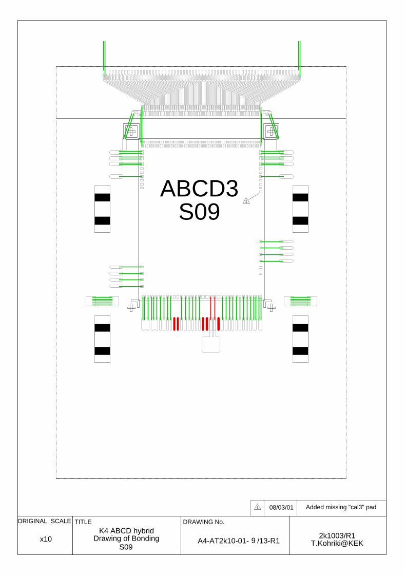
The hybrid wire bond pattern is given in 13 drawings:
1. Overall hybrid schematics
2. Vicinity of individual chips; 12 drawings for the chips, M00, S01, S02, S03, S04, and E05 of the top side and M08, S09, S10, S11, S12, and E13 of the back side. Bond patterns to the pitch adaptor are also included.
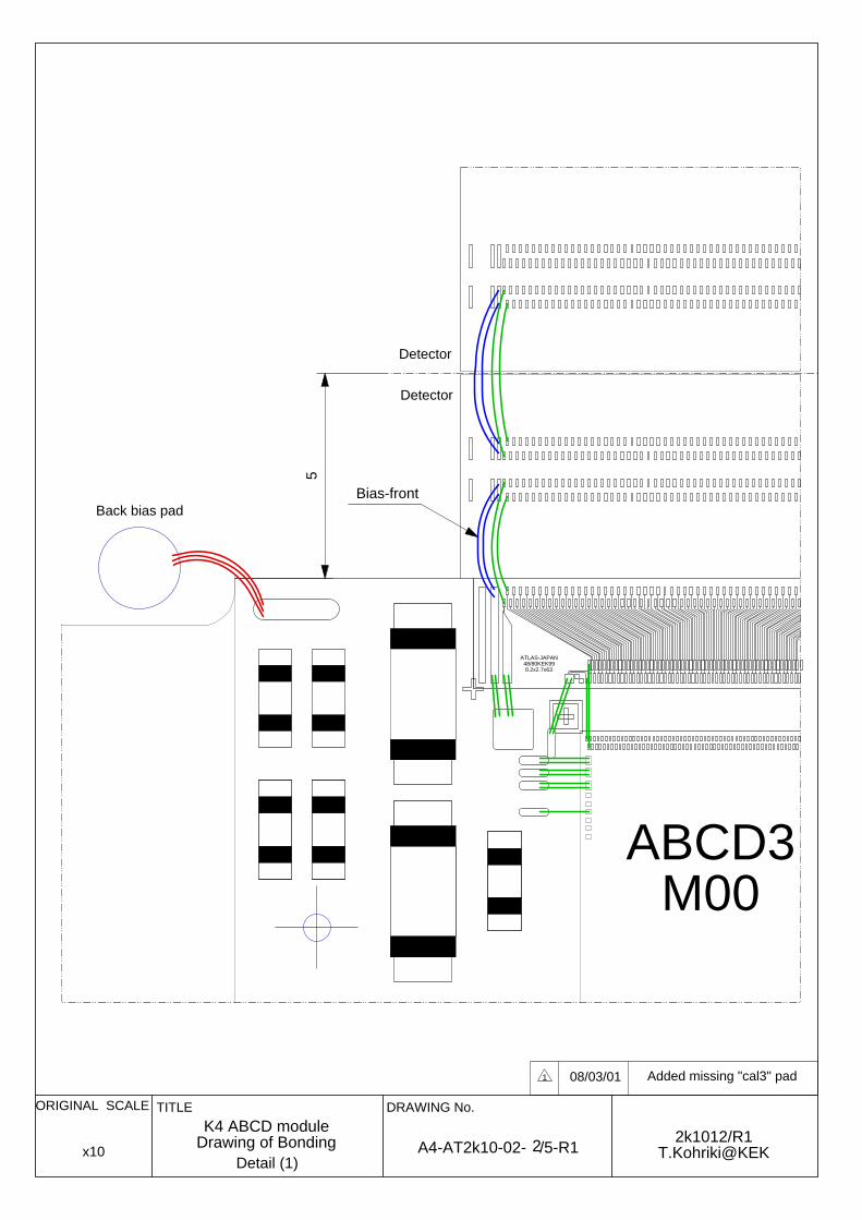
Following these drawings, the wire bond patterns between the hybrid and the sensor-baseboardassembly are given in 5 drawings:
3. Overall schematics of the sensor-baseboard and the hybrid
4. Vicinity of the four corners where the sensor bias connections are being made.
In the drawings, wire bonds are colour-classified as
Green: common to all chips
Red: specific pattern to the chips
Blue: HV connections.
Number of pads has multiple wires drawn in the drawings. These are actual number of wires tobe made. Repetition of wire bonds, e.g., individual channels of chips, is abbreviated.

ATLAS Project Document No. Page:
Rev. No.:
4 of 4
ATL-xx-xx-xxxxB
3 Wire bond loop heights
In order to have a good pull strength, the wire bond loop height recommended is about 20~25%of the bonds distance. Table 1 gives an example of the barrel module built at KEK. In the table,the symbols shows
L: bonds distance
H: height difference of pads
h: loop height over the higher pad
ratio: h/L.
References
[1] Author(s), “Title”, reference id, date
Table 1 Wire bond loop heights of an example of KEK modules
Bond L [mm] H [mm] h [mm] Ratio (h/L)
Sensor-sensor long 4.0 0 0.94 24%
Sensor-sensor short 3.3 0 0.63 19%
Sensor-pitch adaptor long 2.9 1.2 0.78 27%
Sensor-pitch adaptor short 2.3 1.2 0.48 21%
Pitch adaptor-chip long 2.0 0.32 0.49 25%
Pitch adaptor-chip short 1.5 0.32 0.29 19%
Chip-hybrid 1.3 0.51 0.28 22%

ABCD3ABCD3C1 C2 C3 C4 C5 C6
C15 C16 C17 C18 C19 C20C51 (330 nF)
C52 (330 nF)
C71 (10nF, 630V)
C72 (10nF, 630V)
TM1
R36 (0k)
R33 (5k)
R34 (5k)
R35 (1k)
M00 S01 S02 S03 S04 E05
Pitchadaptor
C7
C21
C53 (330nF)
C54 (330nF)
C73 (10nF, 630V)
E05
C8 C9 C10 C11 C12 C13 C14
C22 C23 C24 C25 C26
C28
C55 (330nF)
C27C56
C57 (330nF)
C58
C74 (10nF, 630V) C75 (10nF, 630V)
TM2 R27 R28R29
R30 (100 ohm)
M08 S09 S10 S11 S12 E13
Pitch Adapter
ABCD3 ABCD3 ABCD3
ABCD3 ABCD3 ABCD3 ABCD3 ABCD3 ABCD3
Components of theABCD3T Cu/Polyimide Hybrid99.2.12 T.Kondo99.4.15, 99.5.1800.1.10, 00.1.25,00.2.9, 00.2.14,00.5.11, 00.8.2201.3.09
Refer the Circuit-diagram version (2000.7.12) or later for component numbers
C1~C28 : Murata GRM39X7R224K10C51~C58 : Murata GRM42-6X7R334K50C71~75 : Murata GHM1530X7R103K630
Temp. sensor
Temp. sensor

ABCD3M00
193
21.3
8.4 74.6
25.1
35.4
Scale x0.8
ABCD3S01
ABCD3S02
ABCD3S03
ABCD3S04
ABCD3E05
ABCD3M08
ABCD3S09
ABCD3S10
ABCD3S11
ABCD3S12
ABCD3E13
ATLAS-JAPAN48/80KEK990.2x2.7x63
ATLAS-JAPAN48/80KEK990.2x2.7x63
11 21 31 41 51 61 71 81 91 101 111 121 131 141 151 161 171 181 191 201 211 221 231 241 251 261 271 281 291 301 311 321 331 341 351 361 371 381 391 401 411 421 431 441 451 461 471 481 491 501 511 521 531 541 551 561 571 581 591 601 611 621 631 641 651 661 671 681 691 701 711 721 731 741 751 761
A
A
B
D
C D
B
C
74.6
ID4SELECT
VDD
DGND
TM
ATLAS-JAPAN48/80KEK990.2x2.7x63
ATLAS-JAPAN48/80KEK990.2x2.7x63
11 21 31 41 51 61 71 81 91 101 111 121 131 141 151 161 171 181 191 201 211 221 231 241 251 261 271 281 291 301 311 321 331 341 351 361 371 381 391 401 411 421 431 441 451 461 471 481 491 501 511 521 531 541 551 561 571 581 591 601 611 621 631 641 651 661 671 681 691 701 711 721 731 741 751 761
1All
x2(x1/4) 2k1003/R1T.Kohriki@KEKA4-AT2k10-01- /13-R1
ORIGINAL SCALE TITLE DRAWING No.
K4 ABCD hybridDrawing of Bonding
08/03/011 Added missing "cal3" pad

ATLAS-JAPAN48/80KEK990.2x2.7x63
ABCD3M00
Back bias padDet.ch.1
Det.ch.0Front bias pad
M00
ID4SELECT
VDD
2
1
x10 2k1003/R1T.Kohriki@KEKA4-AT2k10-01- /13-R1
ORIGINAL SCALE TITLE DRAWING No.
K4 ABCD hybridDrawing of Bonding
08/03/011 Added missing "cal3" pad

ABCD3S01
S01
1
3x10 2k1003/R1T.Kohriki@KEKA4-AT2k10-01- /13-R1
ORIGINAL SCALE TITLE DRAWING No.
K4 ABCD hybridDrawing of Bonding
08/03/011 Added missing "cal3" pad

ABCD3S02
S02
1
4x10 2k1003/R1T.Kohriki@KEKA4-AT2k10-01- /13-R1
ORIGINAL SCALE TITLE DRAWING No.
K4 ABCD hybridDrawing of Bonding
08/03/011 Added missing "cal3" pad

ABCD3S03
S03
1
5x10 2k1003/R1T.Kohriki@KEKA4-AT2k10-01- /13-R1
ORIGINAL SCALE TITLE DRAWING No.
K4 ABCD hybridDrawing of Bonding
08/03/011 Added missing "cal3" pad

ABCD3S04
S04
1
6x10 2k1003/R1T.Kohriki@KEKA4-AT2k10-01- /13-R1
ORIGINAL SCALE TITLE DRAWING No.
K4 ABCD hybridDrawing of Bonding
08/03/011 Added missing "cal3" pad

ATLAS-JAPAN48/80KEK990.2x2.7x63
ABCD3E05
Back bias pad
Front bias padDet.ch.769
Det.ch.770
DGND
TM
1
E057x10 2k1003/R1
T.Kohriki@KEKA4-AT2k10-01- /13-R1
ORIGINAL SCALE TITLE DRAWING No.
K4 ABCD hybridDrawing of Bonding
08/03/011 Added missing "cal3" pad

ABCD3M08
M08
ATLAS-JAPAN48/80KEK990.2x2.7x63
Det.ch.1
Det.ch.0Front bias pad
1
8x10 2k1003/R1T.Kohriki@KEKA4-AT2k10-01- /13-R1
ORIGINAL SCALE TITLE DRAWING No.
K4 ABCD hybridDrawing of Bonding
08/03/011 Added missing "cal3" pad
S09
ABCD3S09
1
9x10 2k1003/R1T.Kohriki@KEKA4-AT2k10-01- /13-R1
ORIGINAL SCALE TITLE DRAWING No.
K4 ABCD hybridDrawing of Bonding
08/03/011 Added missing "cal3" pad

S10
ABCD3S10
1
10x10 2k1003/R1T.Kohriki@KEKA4-AT2k10-01- /13-R1
ORIGINAL SCALE TITLE DRAWING No.
K4 ABCD hybridDrawing of Bonding
08/03/011 Added missing "cal3" pad

S11
ABCD3S11
1
11x10 2k1003/R1T.Kohriki@KEKA4-AT2k10-01- /13-R1
ORIGINAL SCALE TITLE DRAWING No.
K4 ABCD hybridDrawing of Bonding
08/03/011 Added missing "cal3" pad

S12
ABCD3S12
1
12x10 2k1003/R1T.Kohriki@KEKA4-AT2k10-01- /13-R1
ORIGINAL SCALE TITLE DRAWING No.
K4 ABCD hybridDrawing of Bonding
08/03/011 Added missing "cal3" pad

E13
ABCD3E13
ATLAS-JAPAN48/80KEK990.2x2.7x63
Front bias padDet.ch.769
Det.ch.770
1
13x10 2k1003/R1T.Kohriki@KEKA4-AT2k10-01- /13-R1
ORIGINAL SCALE TITLE DRAWING No.
K4 ABCD hybridDrawing of Bonding
08/03/011 Added missing "cal3" pad

- 20
mR
ad. F
ace
+ 2
0 m
Rad
. Fac
eA B
C D
C D
AB
1
2
3
4
All1
x1 2k1012/R1T.Kohriki@KEKA4-AT2k10-02- /5-R1
ORIGINAL SCALE TITLE DRAWING No.
K4 ABCD moduleDrawing of Bonding
08/03/011 Added missing "cal3" pad
Detector
Bias-front
ATLAS-JAPAN48/80KEK990.2x2.7x63
ABCD3M00
Back bias pad
x10Detail (1)
5
Detector
2 2k1012/R1T.Kohriki@KEKA4-AT2k10-02- /5-R1
ORIGINAL SCALE TITLE DRAWING No.
K4 ABCD moduleDrawing of Bonding
08/03/011 Added missing "cal3" pad

ATLAS-JAPAN48/80KEK990.2x2.7x63
Detector
Bias-frontBack bias pad
x10Detail (2)
Detector
5
ABCD3E05 1
32k1012/R1
T.Kohriki@KEKA4-AT2k10-02- /5-R1
ORIGINAL SCALE TITLE DRAWING No.
K4 ABCD moduleDrawing of Bonding
08/03/011 Added missing "cal3" pad

Detector
Bias-front
ATLAS-JAPAN48/80KEK990.2x2.7x63
x10Detail (3)
5
Detector
ABCD3M08
4 2k1012/R1T.Kohriki@KEKA4-AT2k10-02- /5-R1
ORIGINAL SCALE TITLE DRAWING No.
K4 ABCD moduleDrawing of Bonding
08/03/011 Added missing "cal3" pad

ATLAS-JAPAN48/80KEK990.2x2.7x63
Detector
Bias-front
x10Detail (4)
Detector
5
ABCD3E13 1
5 2k1012/R1T.Kohriki@KEKA4-AT2k10-02- /5-R1
ORIGINAL SCALE TITLE DRAWING No.
K4 ABCD moduleDrawing of Bonding
08/03/011 Added missing "cal3" pad