AND8246/D A 160 W CRT TV Power Supply using NCP1337
10
© Semiconductor Components Industries, LLC, 2005 November, 2005 - Rev. 1 1 Publication Order Number: AND8246/D AND8246/D A 160 W CRT TV Power Supply using NCP1337 Prepared by: Nicolas Cyr ON Semiconductor Introduction Valley switching converters, also known as quasi-resonant (QR) converters, allow designing flyback Switch-Mode Power Supplies (SMPS) with reduced Electro-Magnetic Interference (EMI) signature and improved efficiency. Thanks to the low level of generated noise, valley switching SMPS converters are therefore very well suited to applications dealing with RF and video signals, such as TVs. ON Semiconductor NCP1337 is a powerful valley switching controller, which eases the design of an EMI-friendly TV power supply with only a few surrounding components. Moreover, very low standby power (less than 1 W) can be achieved without any noise. Main Features of the Controller • Automatic Valley Switching • Current-Mode • Soft Ripple Mode with Minimum Switching Frequency for Noise-Free Standby • Auto-Recovery Short-Circuit Protection Independent of Auxiliary Voltage • Over Voltage Protection • Brown-Out Protection • 2 Externally Triggerable Fault Comparators (Auto-Recovery or Permanent Latch) • Internal 5 ms Soft-Start • 500 mA Peak Current Source/Sink Capability • 130 kHz Max Frequency • Internal Leading Edge Blanking • Internal Temperature Shutdown • Direct Optocoupler Connection • Dynamic Self-Supply A 160 W TV Power Supply Design Power Supply Specification Input Voltage Universal input 90 Vac to 265 Vac Output Power 160 W Outputs +135 V, 1 A max (135 W) regulated +20 V, 800 mA max (16 W) +12 V, 500 mA max (6 W) +8 V, 500 mA max (4 W) Standby output : +5 V, 100 mA derived from +8 V through a regulator Protections Short-circuit, over-power, over-voltage and brown-out Standby Power below 1 W APPLICATION NOTE http://onsemi.com
Transcript of AND8246/D A 160 W CRT TV Power Supply using NCP1337

© Semiconductor Components Industries, LLC, 2005
November, 2005 − Rev. 11 Publication Order Number:
AND8246/D
AND8246/D
A 160 W CRT TV PowerSupply using NCP1337
Prepared by: Nicolas CyrON Semiconductor
IntroductionValley switching converters, also known as
quasi−resonant (QR) converters, allow designing flybackSwitch−Mode Power Supplies (SMPS) with reducedElectro−Magnetic Interference (EMI) signature andimproved efficiency. Thanks to the low level of generatednoise, valley switching SMPS converters are therefore verywell suited to applications dealing with RF and videosignals, such as TVs.
ON Semiconductor NCP1337 is a powerful valleyswitching controller, which eases the design of anEMI−friendly TV power supply with only a few surroundingcomponents. Moreover, very low standby power (less than1 W) can be achieved without any noise.
Main Features of the Controller• Automatic Valley Switching
• Current−Mode
• Soft Ripple Mode with Minimum Switching Frequencyfor Noise−Free Standby
• Auto−Recovery Short−Circuit Protection Independentof Auxiliary Voltage
• Over Voltage Protection
• Brown−Out Protection
• 2 Externally Triggerable Fault Comparators(Auto−Recovery or Permanent Latch)
• Internal 5 ms Soft−Start
• 500 mA Peak Current Source/Sink Capability
• 130 kHz Max Frequency
• Internal Leading Edge Blanking
• Internal Temperature Shutdown
• Direct Optocoupler Connection
• Dynamic Self−Supply
A 160 W TV Power Supply Design
Power Supply Specification
Input Voltage Universal input 90 Vac to 265 Vac
Output Power 160 W
Outputs +135 V, 1 A max (135 W) regulated+20 V, 800 mA max (16 W)+12 V, 500 mA max (6 W)+8 V, 500 mA max (4 W)
Standby output :+5 V, 100 mA derived from +8 V througha regulator
Protections Short−circuit, over−power, over−voltageand brown−out
Standby Power below 1 W
APPLICATION NOTE
http://onsemi.com

AND8246/D
http://onsemi.com2
Schematic
1
2
3
4 5
8
6
7
C10
Rs1
Rbo2
Rbo1
D7
R3
D6
R2 C8
D13
C20
D12
R8
R12
R11
C25
D111
C7
D14
DZ2C16
135V
8V
20V
IC2
C141
IC1
X1
C131
C15
Rs2
C19
C9
IC3x
IC3
R1
D10
R4
C23
R7
R10
P1
SW1
R16
T1
0V
C11
C12 R19
C5
mains
F1
D5
L1
C1
C2
D1
R31
Rhyst
R6
R18
R17
R13
C3
R5
C21
Q1R21
D11
12V
C14C13
R33
R34
DZ3
IN OUT
ADJUST
IC45Vstby
C17
Reg 5VD16
Out12V
Out20V
Out8V
Out20V
Out12V
Out8V
C18
D141
C42
4
6
8
15
16
11
12
13
14
17
18
RboC26
M1
R35
AND8246/D
http://onsemi.com3
Design Steps
1. Reflected VoltageLet us first start the design by selecting the amount of
secondary voltage we want to reflect on the primary side,which will give us the primary to secondary turn ratio of thetransformer. If we decide that we want to use a rather cheapand common 600 V MOSFET, we will select the turn ratioby:
VINmax � N · (VOUT � VF) � 600 V
VINmax is 375 V and (VOUT + VF) is about 135.5 V. If wedecide to keep a 100 V safety margin, it gives N < 0.92. Wewill choose a turn ratio of N = 0.91, which will give areflected voltage of 123 V.
2. Peak CurrentKnowing the turn ratio, we can now calculate the peak
primary current needed to supply the 75 W of output power.If we neglect the delay TW between the zero of the currentand the valley of the drain voltage, we can calculate IPmaxby:
IPmax � 2 · POUT ·VINmin � N · (VOUT � VF)
� · N · VINmin · (VOUT � VF)
VINmin is 110 V and η is 85%. Plugging the other valuesgives us a maximum peak current of IPmax = 6.5 A.NCP1337 max current sense setpoint is 500 mV, so weshould put a sense resistor RS = 0.5 V / 6.5 A = 0.077 �. Wewill use two standard 0.15 � resistors in parallel, that willallow IPmax = 6.67 A.
3. Primary InductanceTo calculate the primary inductance LP, we need to decide
the switching frequency range in which we allow thecontroller to operate. There are two constraints: at low line,maximum power, the switching frequency should be abovethe audible range (higher than 20 kHz). At high line, 50%nominal power, the switching period should be higher than7.5 �s, to prevent the controller from jumping betweenvalleys (because these discrete jumps between 2 valleys cangenerate noise in the transformer as well). If we still neglectTW, LP is then given by:
LP � 1
2 · FSWmin · POUTmax� VINmin�N · (VOUT�VF)
� · N · VINmin · (VOUT�VF)�2
If we choose 20 kHz min for 160 W of output power at110 Vdc, we obtain: LP � 380 �H.
To take tolerances into account, we can choose LP =330 �H, and verify if it satisfies the second condition:
For 80 W output power at 375 Vdc, TSW = 9 �s, i.e.FSW = 112 kHz.
4. ClampWe can calculate the overvoltage due to the leakage
inductance: VOVLEAK � IPLLEAKCTOT
� .
At this time we don’t know the value of LLEAK, but wecan choose a value of 3% of the primary inductance (i.e.10��H), which would not be too far from the final value.Considering 330 pF on the drain, at 375 V input voltageand 160 W of output power, which gives IP = 4.2 A, weobtain: VOVLEAK � 730 V.
But we only have 100 V available before reaching theMOSFET breakdown voltage. So we will need to add aclamp to limit the spike at turn−off.
Please refer to application note AN1679 (available atwww.onsemi.com) to calculate this clamp. You can also usea SPICE simulator to test the right values for thecomponents.
We chose to use an RCD clamp, using a 1N4937 diode, a47 k� resistor and a 10 nF capacitor: it is an aggressivedesign (the maximum drain voltage will be very close to themaximum voltage allowable for the MOSFET), but it givesenough protection without degrading the efficiency toomuch.
5. Brown−Out ProtectionWe want the power supply to turn on at 90 Vac, and turn
off at 70 Vac.Start−up level is directly given by the resistor divider
connected between high input voltage and BO pin, knowingthat the threshold of the internal comparator is 500 mV.90 Vac means 127 Vdc, so the ratio of the divider must be254.
Once the controller has started, an internal 10 �A currentsource is activated and flows out of BO pin, creatinghysteresis. 70 Vac means 99 Vdc, so we want a 28 Vhysteresis, corresponding to 22% of the start−up level. Thecorresponding threshold for the comparator is 390 mV, sothe 10 �A current must create an offset of 110 mV across theequivalent resistance of the resistor divider.
Those 2 conditions lead to 2 equations:
RBOhigh � RBOlowRBOlow
� 254
and
RBOhigh · RBOlowRBOhigh � RBOlow
· 10−5 � 0.11
Solving these equations gives RBOhigh = 2.8 M� andRBOlow = 11 k�.
But in reality there will be a non−negligible ripple on theDC input voltage, and the hysteresis should be increased inorder to obtain the desired turn−on and turn−off levels.
Final value for RBOlow is 15k (RBO2 in schematic), and3.9 M� for RBOhigh (split in RBO = 2.7 M� and RBO1 =1.2 M� to sustain the high voltage).
A capacitor C7 is added between BO pin and ground tofilter any noise, and to ensure a DC voltage. This capacitorvalue should be small enough, otherwise it may introduce adelay between input voltage collapsing and Power supplyturn−off (a 10 nF ceramic capacitor gives good results).

AND8246/D
http://onsemi.com4
6. Overpower ProtectionWe have seen that full load maximum peak current at low
input voltage is 6.5 A, but only 4.2 A at high input voltage.We need to create an offset on the current sense signal. As500 mV on CS pin corresponds to 6.67 A, 2.3 A correspondsto a 172 mV offset. At 375 Vdc input voltage, BO voltage is1.55 mV: as a result a 73.5 �A current flows out of CS pinduring ON time. To create the desired 172 mV offset, it isnecessary to insert a 2.34 k� resistor R6 in series. We choosea standard 2.2 k� value.
7. StandbyIn order to reduce as much as possible the power wasted
during standby mode, NCP1337 enters an efficient and quietsoft−skip mode. But because of the high output voltage of135 V, any leakage current will create a significant outputpower, preventing the power supply to reach therequirement of less than 1 W standby power. Thisdemonstration board thus includes a simple patented circuitthat allows collapsing all unused outputs, while stillpowering the 5 V standby rail. This circuit is made of aregulated rectifier (around M1) connected between the highvoltage output winding and the input of the 5 V linearregulator IC4, and of a switch (Q1) that changes theregulation setpoint. DZ2 is added to prevent voltage dropsduring transition from normal to standby mode.
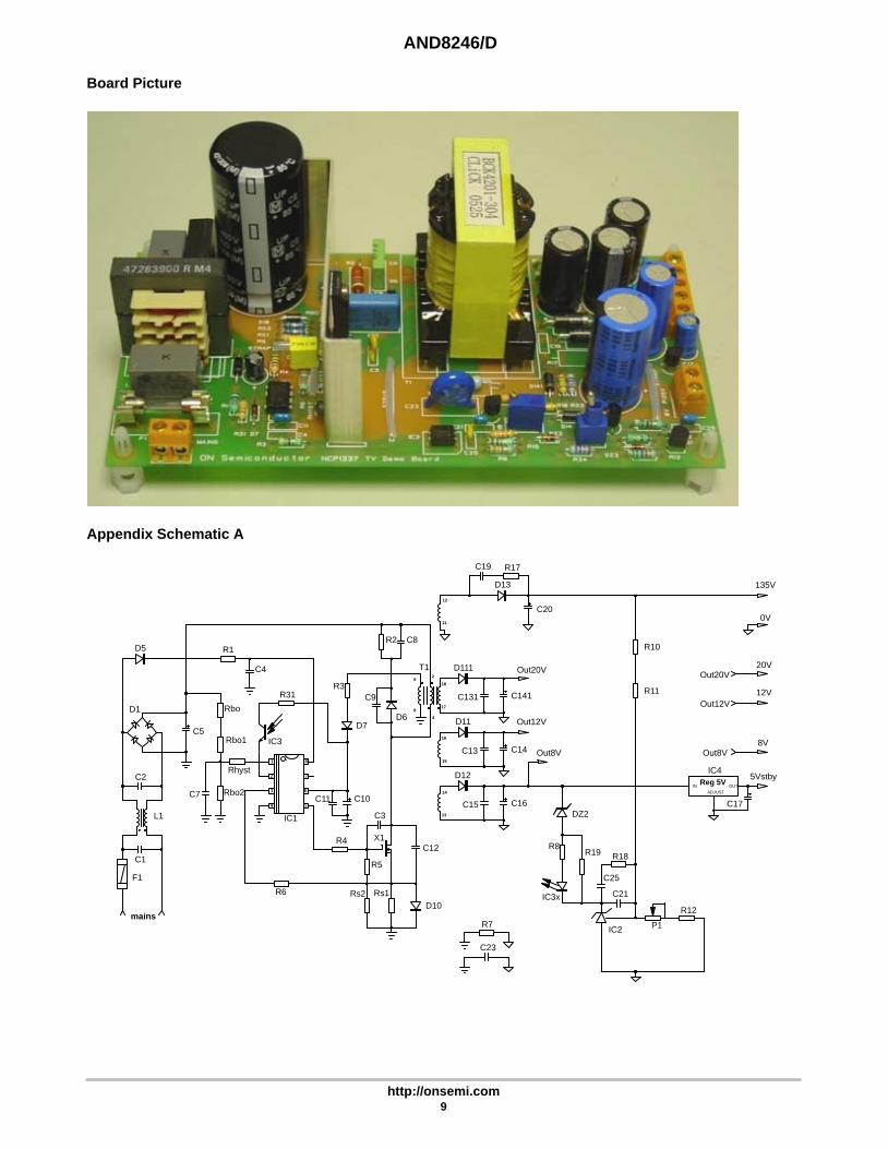
If the leakage current on the 135 V output is extremelylow, this circuit can be omitted (see appendix schematic A).
8. Controller SupplyNCP1337 includes a DSS able to supply the controller
without the help of any auxiliary supply. However this ispossible only if the gate current is low, i.e. during standby inour case. So an auxiliary winding is necessary to supply thecontroller during normal mode, but DSS can be activated instandby, for instance in the case all voltages are decreased bythe circuit described above. In order to minimize the powerconsumption of the DSS, HV pin can be connected to thehalf−wave rectified input voltage instead of the full−waverectified bulk voltage.
To further decrease the power consumed by the controllerduring standby, it may be interesting to prevent the DSS toturn on: this can be achieved by inverting the coupling of theauxiliary winding (see appendix schematic B). By creatingthe auxiliary supply from a forward winding instead of aflyback winding, it is possible to ensure a sufficient supplyvoltage even in standby mode with all voltages reduced.VCC voltage must then be clamped to protect the controller
when the input voltage is high: as a result overvoltageprotection on VCC pin is lost.
Static Measurements
Brown−Out Protection• Input voltage turn−ON level: 95 Vac
• Input voltage turn−OFF level: 80 Vac
Efficiency• At 230 Vac, 148 W IN for 135 W OUT 91%
• At 110 Vac, 154 W IN for 135 W OUT 87%
Standby Power• Noise−free
• All outputs are low (135 V output is 12.7 V), except5 V standby output which is maintained. IOUTconsumption is taken on 5 V standby output. Controlleris powered thanks to the Dynamic Self−Supply (DSS).
IOUT
VIN
0 10 20 30 40
230 Vac 390 mW 600 mW 780 mW 980 mW 1.18 W
110 Vac 230 mW 460 mW 700 mW 860 mW 975 mW
• All outputs are low (135 V output is 12.7 V), except5 V standby output which is maintained. IOUTconsumption is taken on 5 V standby output. Controlleris powered thanks to a forward−coupled auxiliarywinding.
IOUT
VIN
0 10 20 30 40
230 Vac 340 mW 470 mW 580 mW 730 mW 900 mW
110 Vac 140 mW 350 mW 540 mW 700 mW 820 mW
• All outputs are at their nominal values. IOUTconsumption is taken on 5 V standby output. Controlleris powered thanks to the auxiliary winding.
IOUT
VIN
0 10 20 30 40
230 Vac 260 mW 380 mW 620 mW 740 mW 880 mW
110 Vac 180 mW 280 mW 400 mW 540 mW 690 mW

AND8246/D
http://onsemi.com5
Static Measurements
Soft−Start
At 230 Vac, full load At 110 Vac, no load
CS
Drain Drain
CS
At 230 Vac, no load At 110 Vac, no load
CS
Drain
CS
Drain

AND8246/D
http://onsemi.com6
Valley Switching
At 230 Vac, full load At 110 Vac, full load
At 230 Vac, half load At 110 Vac, half load
Load Transients
At 230 Vac, 20% to 80% load on 135 V output At 110 Vac, 20% to 80% load on 135 V output

AND8246/D
http://onsemi.com7
Standby
Standby burst at 110 Vac
Vcc Vcc
Standby burst at 230 Vac
Vcc Vcc
Transitions Between Modes
Normal to Standby Transition Standby to Normal Transition
5V Standby
135V output
135V output
5V Standby
AND8246/D
http://onsemi.com8
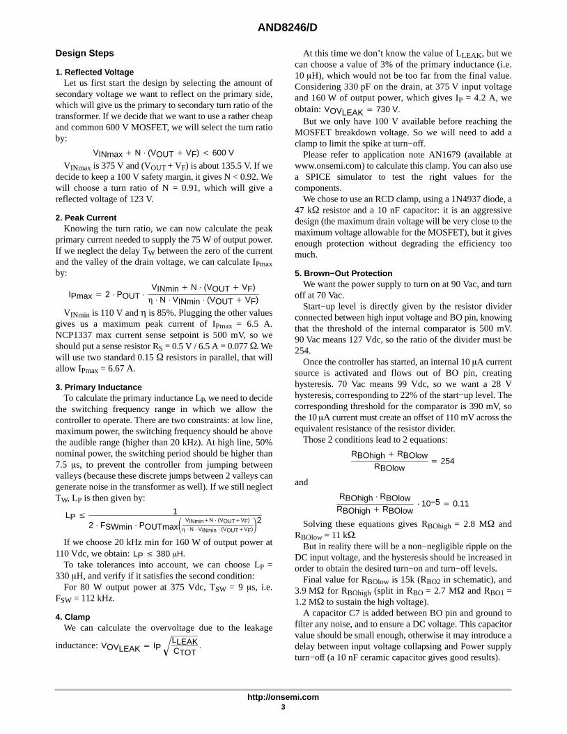
Board Layout
AC input
20V12V
8V5V
135V
Standby switch:Left: normal modeRight: standby mode
Bill of Material
2.2kR60.15Rs1, Rs233kR5, R2115R447R3−Rhyst15kRbo21.2MegRbo12.7MegRbo47k −2WR21kR1, R356V2DZ33V9DZ2MUR460D13MUR420D11, D12, D1111N4148D71N4937D61N4007D5, D10, D14, D16, D141KBU4KD12A 250VF1OREGA 47283900 RM4L1
CLICK BCK4201−304T1BC547Q1BS108M1IRFIB6N60AX1MC78L05IC4SFH615AIC3TL431IC2NCP1337IC1
47k −
TDK SRW42/15EC−X21V017,
470nC262.2n −Y1C231nC21100u −200VC201000u −16VC18100u −25VC171000u −35VC14, C16, C141330p −1.5kVC12100nC11, C13, C15, C25, C131
33u −25VC10−C910n −630VC81u −63VC7220u −450VC5−C410p −2kVC3330p −300Vac −X2C1, C21kP147kR33,R341.5kR1918kR18, R31−R17100kR13, R165.6kR12120kR11150kR10330R810Meg −R7
2.2n Y1
−200V−16V
100u 25V−35V
330p −
33u −
10n −1u −220u 450V
10p −330p − −X2
−4kV
AND8246/D
http://onsemi.com9
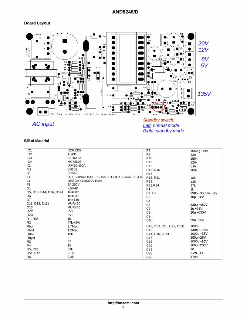
Board Picture
Appendix Schematic A
1
2
3
4 5
8
6
7
C10
Rs1
Rbo2
Rbo1
D7
R3
D6
R2 C8
D13
C20
D12
R8
R12
R11
C25
D111
C7
DZ2C16
135V
8V
20V
IC2
C141
IC1
X1
C131
C15
Rs2
C19
C9
IC3x
IC3
R1
D10
R4
C23
R7
R10
P1
T1
0V
C11
C12 R19
C5
mains
F1
D5
L1
C1
C2
D1
R31
Rhyst
R6
R18
R17
C3
R5
C21
D11
12V
C14C13
IN OUTADJUST
IC45Vstby
C17
Reg 5V
Out12V
Out20V
Out8V
Out20V
Out12V
Out8V
C42
4
6
8
15
16
11
12
13
14
17
18
Rbo

AND8246/D
http://onsemi.com10
Appendix Schematic B
1
2
3
4 5
8
6
7
C10
Rs1
Rbo2
Rbo1
D7
R3
D6
R2 C8
D13
C20
D12
R8
R12
R11
C25
D111
C7
D14
DZ2C16
135V
8V
20V
IC2
C141
IC1
X1
C131
C15
Rs2
C19
C9
IC3x
IC3
R1
D10
R4
C23
R7
R10
P1
SW1
R16
T1
0V
C11
C12 R19
C5
mains
F1
D5
L1
C1
C2
D1
R31
Rhyst
R6
R18
R17
R13
C3
R5
C21
Q1R21
D11
12V
C14C13
R33
R34
DZ3
IN OUT
ADJUST
IC45Vstby
C17
Reg 5VD16
Out12V
Out20V
Out8V
Out20V
Out12V
Out8V
C18
D141
C42
4
6
8
15
16
11
12
13
14
17
18
Rbo
C26
M1
R35
DZ1
ON Semiconductor and are registered trademarks of Semiconductor Components Industries, LLC (SCILLC). SCILLC reserves the right to make changes without further noticeto any products herein. SCILLC makes no warranty, representation or guarantee regarding the suitability of its products for any particular purpose, nor does SCILLC assume any liabilityarising out of the application or use of any product or circuit, and specifically disclaims any and all liability, including without limitation special, consequential or incidental damages.“Typical” parameters which may be provided in SCILLC data sheets and/or specifications can and do vary in different applications and actual performance may vary over time. Alloperating parameters, including “Typicals” must be validated for each customer application by customer’s technical experts. SCILLC does not convey any license under its patent rightsnor the rights of others. SCILLC products are not designed, intended, or authorized for use as components in systems intended for surgical implant into the body, or other applicationsintended to support or sustain life, or for any other application in which the failure of the SCILLC product could create a situation where personal injury or death may occur. ShouldBuyer purchase or use SCILLC products for any such unintended or unauthorized application, Buyer shall indemnify and hold SCILLC and its officers, employees, subsidiaries, affiliates,and distributors harmless against all claims, costs, damages, and expenses, and reasonable attorney fees arising out of, directly or indirectly, any claim of personal injury or deathassociated with such unintended or unauthorized use, even if such claim alleges that SCILLC was negligent regarding the design or manufacture of the part. SCILLC is an EqualOpportunity/Affirmative Action Employer. This literature is subject to all applicable copyright laws and is not for resale in any manner.
PUBLICATION ORDERING INFORMATIONN. American Technical Support: 800−282−9855 Toll FreeUSA/Canada
Japan: ON Semiconductor, Japan Customer Focus Center2−9−1 Kamimeguro, Meguro−ku, Tokyo, Japan 153−0051Phone: 81−3−5773−3850
AND8246/D
LITERATURE FULFILLMENT:Literature Distribution Center for ON SemiconductorP.O. Box 61312, Phoenix, Arizona 85082−1312 USAPhone: 480−829−7710 or 800−344−3860 Toll Free USA/CanadaFax: 480−829−7709 or 800−344−3867 Toll Free USA/CanadaEmail: [email protected]
ON Semiconductor Website: http://onsemi.com
Order Literature: http://www.onsemi.com/litorder
For additional information, please contact yourlocal Sales Representative.