ANALYSIS OF LOSSY SIW STRUCTURES BASED ON … · ANALYSIS OF LOSSY SIW STRUCTURES BASED ON THE...
13
Progress In Electromagnetics Research C, Vol. 33, 157–169, 2012 ANALYSIS OF LOSSY SIW STRUCTURES BASED ON THE PARALLEL PLATES WAVEGUIDE GREEN’S FUNCTION G. Amendola * , E. Arnieri, and L. Boccia Dipartimento di Elettronica, Informatica e Sistemistica, Universit` a della Calabria, Rende (CS) 87036, Italy Abstract—In this paper, a full-wave analysis technique of lossy substrate integrated waveguides, based on the dyadic Green’s function of the parallel plate waveguide, is presented. The field inside the waveguide is expressed in terms of cylindrical vector wave-functions and the finite conductivity of the top and of the bottom plates, and of the metallic vias are taken into account. Losses into the dielectric substrate are also included. Coaxial ports are considered as sources and self and mutual admittances are evaluated. Cases of practical structure taken from literature are presented showing a very good agreement with the most used commercial software. 1. INTRODUCTION The analysis of substrate integrated waveguide (SIW) [1] structures can be efficiently tackled using commercially available software packages. In fact, a considerable number of SIW based devices designed using commercial codes, like HFSS (Ansys HFSS), have been presented over the years. Filters [2–4, 23, 24], power dividers [5–7], antennas [8, 9, 25] and other devices have been successfully designed and realized. However, more effective analysis methods can be devised implementing techniques that, even less general than the one used in commercial codes, are more efficient in terms of both CPU time and occupied memory. Recently, several techniques have been proposed that may significantly shorten the design and optimization process. In [10] the Boundary Integral Resonant Modes Expansion (BIRME) has been adapted to analyze efficiently post walled structures, in [11–13] SIWs have been analyzed considering only the presence of the parallel plate Received 16 August 2012, Accepted 7 October 2012, Scheduled 8 October 2012 * Corresponding author: Giandomenico Amendola ([email protected]).
Transcript of ANALYSIS OF LOSSY SIW STRUCTURES BASED ON … · ANALYSIS OF LOSSY SIW STRUCTURES BASED ON THE...
Progress In Electromagnetics Research C, Vol. 33, 157–169, 2012
ANALYSIS OF LOSSY SIW STRUCTURES BASEDON THE PARALLEL PLATES WAVEGUIDE GREEN’SFUNCTION
G. Amendola*, E. Arnieri, and L. Boccia
Dipartimento di Elettronica, Informatica e Sistemistica, Universitadella Calabria, Rende (CS) 87036, Italy
Abstract—In this paper, a full-wave analysis technique of lossysubstrate integrated waveguides, based on the dyadic Green’s functionof the parallel plate waveguide, is presented. The field inside thewaveguide is expressed in terms of cylindrical vector wave-functionsand the finite conductivity of the top and of the bottom plates, andof the metallic vias are taken into account. Losses into the dielectricsubstrate are also included. Coaxial ports are considered as sources andself and mutual admittances are evaluated. Cases of practical structuretaken from literature are presented showing a very good agreementwith the most used commercial software.
1. INTRODUCTION
The analysis of substrate integrated waveguide (SIW) [1] structures canbe efficiently tackled using commercially available software packages.In fact, a considerable number of SIW based devices designed usingcommercial codes, like HFSS (Ansys HFSS), have been presented overthe years. Filters [2–4, 23, 24], power dividers [5–7], antennas [8, 9, 25]and other devices have been successfully designed and realized.However, more effective analysis methods can be devised implementingtechniques that, even less general than the one used in commercialcodes, are more efficient in terms of both CPU time and occupiedmemory. Recently, several techniques have been proposed that maysignificantly shorten the design and optimization process. In [10] theBoundary Integral Resonant Modes Expansion (BIRME) has beenadapted to analyze efficiently post walled structures, in [11–13] SIWshave been analyzed considering only the presence of the parallel plate
Received 16 August 2012, Accepted 7 October 2012, Scheduled 8 October 2012* Corresponding author: Giandomenico Amendola ([email protected]).

158 Amendola, Arnieri, and Boccia
waveguide (PPW) TEM mode and taking into account the scatteringby the metallic posts, so reducing the analysis to the solution of a twodimensional problem. In [14] the authors presented a technique basedon the full dyadic Green’s function of the parallel plate, expressed asseries of vector wave functions [16] TE and TM with respect to thewaveguide height. In this last case also, the presence of the metallicvias was included in the analysis solving the scattering problem.The method was also used to determine the characteristics of SIWresonators [17] and to analyze SIW based slot arrays [18]. In thispaper we present the extension of the technique presented in [14],which treated only lossless case, to lossy structures. To evaluate thepower dissipated on the metallic surfaces and in the dielectric slab,the dyadic Green’s function is changed to take into account the finiteconductivity of the metallic plates [19] and including the dielectriclosses into the argument of the wave functions. Furthermore, metallicposts are considered to have finite conductivity. As it is well known,for perfectly conducting cylinders, TE and TM mode do not couple.When a TE (or a TM ) wave impinges on a perfectly conductingcylinder a TE (or a TM ) field is scattered by the cylinder. For a finiteconductivity cylinder or, more in general, for an impedance cylinder,this is no more true. However if a cylinder is made of a good conductor,as it is the case in this paper, the coupling between TE and TM wavescan be neglected. This approximation makes the analysis considerablysimpler and, as it will be shown, is valid in the case of SIW.
In this paper, the dyadic Green’s function of the lossy parallelplate waveguide is firstly described. The complete derivation of theGreen’s function has been given in [14] but in this paper a slightlydifferent path starting from the lossless case in [14] and relying on [15]is followed. The scattering by the lossy metallic cylinder, is consideredlater and added to the contribution from PPW. The most useful caseof probe feeding is considered and results from passive devices alreadypresented in literature are presented and discussed.
2. DYADIC GREEN’S FUNCTION OF THE LOSSYPARALLEL PLATES WAVEGUIDE
Following the notation in [14], the dyadic Green’s function is expressedin the spectral domain as a series of cylindrical wave functions
¯GPPW =j
4π
∑∫ ∞
0dkρkρ
[Mn(kρ,±k0z, ρ, z)M−n(kρ,∓k0z,ρ
′, z′)k0zk2
ρ
+Nn(kρ,±k0z, ρ, z)N−n(kρ,∓k0z, ρ
′, z′)k0zk2
ρ
]−zzδ(r−r′)
k20
(1)

Progress In Electromagnetics Research C, Vol. 33, 2012 159
where k0 = ω√
µ0(ε′ + jε′′), k0z =√
k20 − k2
ρ and
Mn = (kρ, k0z,ρ, z) = ∇×(Φn(kρ, ρ, φ)e−jk0zzz
)
Nn = (kρ, k0z,ρ, z) = ∇×∇×(Φn(kρ, ρ, φ)e−jk0zz z
) (2)
withΦn(kρ, ρ, φ) = Jn(kρρ)e−jnφ (3)
The free space Green’s function is then used to find the Green’sfunction of the parallel plate considering the field reflected fromthe conducting plates expanded in terms of the same vector eigen-functions. This procedure, clearly described in [15], leads to
¯GPPW
=− j
4π
∑∫ ∞
0dkρkρ×
[(∇×z)
(∇′×z)Φn(kρ,ρ,φ)Φ−n(kρ,ρ
′,φ′)kzk2
ρ
FTM±
(z, z′
)
+ (∇×∇×z)(∇′ ×∇′ × z
) Φn(kρ, ρ, φ)Φ−n(kρ, ρ′, φ′)
kzk2ρ
FTE±
(z,z′
)]
− 1k2
zzδ(r− r′
)(4)
whereFTM±
(z, z′
)
=
(ejkzz′ + e−jkzz′RTM
) (e−jkzz + ejkz(z−2d)RTM
)
1−R2TM e−j2kzd
for z > z′ (5)
FTM−
(z, z′
)= FTM
+
(z, z′
)for z < z′
FTE± (z, z′) is derived from FTM± (z, z′) substituting RTM with RTE
with [19]
RTM =εckz − εk2z
εckz + εk2zRTE =
kz − k2z
kz + k2z(6)
and k2z =√
k2c − k2
ρ, k2z =√
k2 − k2ρ. The previous expression are
derived considering the top and bottom conducting plates as layerswith dielectric constant εc = −jσ/ω [19].
The spectral integral in (4) is now solved by extending theintegration limits to [−∞, +∞] introducing Hankel’s functions andapplying the residue theorem [19]. One obtains
¯GPPW · ¯It =−14
[∑nm
Mn(kρm, kzm, ρ, z, 2d)M−n(kρm,−kzm, ρ′, z′, 0)DTM ′(kρm)

160 Amendola, Arnieri, and Boccia
+Nn(kρm, kzm, ρ, z, 2d)N−n(kρm,−kzm, ρ′, z′, 0)
DTE ′(kρm)
]· ¯It z>z′ (7)
¯GPPW · ¯It =−14
[∑nm
Mn(kρm,−kzm, ρ, z, 2d)M−n (kρm, kzm, ρ′, z′, 0)DTM ′(kρm)
+Nn(kρm,−kzm, ρ, z, 2d)N−n(kρm, kzm, ρ′, z′, 0)
DTE ′(kρm)
]· ¯It z<z′ (8)
In the previous expressions the transverse components are selected bymeans of the scalar product with the transverse dyad ¯It, d is the heightof the parallel plate and the quantity, kρm is evaluated as residues of
integral (4) [19], kzm =√
k2 − k2ρ and Mn and Nn functions have the
following expressionsMn(kρm, kzm, ρ<>, z,∆z)
=(∇× z){
Jn(kρmρ<)H
(2)n (kρmρ>)
}× e−jnφ
(e−jkzmz + ejkzm(z−∆z)RTM
)(9)
Nn(kρm, kzm, ρ<>, z,∆z)
=1k
(∇×∇×z){
Jn(kρmρ<)H
(2)n (kρmρ>)
}×e−jnφ
(e−jkzmz+ejkzm(z−∆z)RTE
)(10)
where ρ> = max(ρ, ρ′), ρ< = min(ρ, ρ′). Furthermore, DTE ′ and DTM ′
are the derivative with respect to kρ of
DTM = k0zkρ
(1−R2
TM e−j2kzd)
DTE = k0zkρ
(1−R2
TEe−j2kzd) (11)
3. SCATTERING FROM METALLIC VIAS OF FINITECONDUCTIVITY
As pointed out in the introduction, to evaluate the scattering byimpedance cylinders one has to consider both TE and TM fields
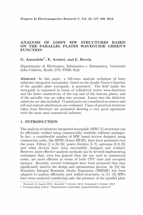
Infinite metallic
Coaxial port iCoaxial port j
Metallic vias
plates
Figure 1. General geometry of a SIW structure with coaxial ports.

Progress In Electromagnetics Research C, Vol. 33, 2012 161
independently from the nature of the exciting field. However, as isknown, vias are made of good conductor and one can consider thatthey scatter mostly TM (TE ) field when the impinging field is TM(TE ) and that the TE (TM ) field is negligible. Under this hypothesisthe scattering from metallic vias is taken into account as in [14] butenforcing the following boundary conditions on the cylinders surface:
ρ×∇×H = −jωεrε0ZsH (12)
with
Zs = (1 + j)√
ωµ0
2σ(13)
The field scattered from vias is expressed as series of outgoing TM andTE waves centered on cylinders
HsCyl =∑
l
∑n,m
Mn(kρm, kzm,ρ− ρl, z, 2d)AMm,n,l
+∑
n,mNn(kρm, kzm,ρ− ρl, z, 2d)AN
m,n,l (14)
where (see Figure 2) l is an index spanning over the cylinders, m and nare relevant to vertical and angular dependencies, ρl is the position ofthe center of the cylinder l, and AM
m,n,l, ANm,n,l are unknown coefficients
to be determined.
s
Figure 2. Coordinate system.

162 Amendola, Arnieri, and Boccia
As it was done in [14], for any cylinder q one has the followingequations, one for the TM mode one for the TE modes correspondingto apex M and N, respectively:
ΓM,Nq,r,m =
∑l 6=q
∑n
LM,Nq,r,m,l,nAM,N
m,n,l + AM.Nm,r,q
LM,Nq,r,m,l,n = TM,N
r,m,qH(2)n−r(kρmρlq)e−j(n−r)φlq
ΓM,Nq,r,m = −TM,N
r,m,qvTMr,m,q
(15)
where
TM,Nr,m,q = − Jr(kρmaq) + ZJ,M
m
H(2)r (kρmaq) + ZH,M
m
ZJ,Mm =
jωεrε0
kρmZsJ
′r(kρmaq)
ZH,Mm =
jωεrε0
kρmZsH
(2)′r (kρmaq)
(16)
and
TM,Nr,m,q =
J ′r(kρmaq) + ZJ,Mm
H(2)′r (kρmaq) + ZH,N
m
ZJ,Nm =
kρm
jωµ0ZsJr(kρmaq)
ZH,Mm =
kρm
jωµ0ZsH
(2)r (kρmaq)
(17)
In the previous formulas vMr,m,q and vN
r,m,q are expressed as
vMr,m,q =
jωεrε0
4DTM ′(kρm)×∫
dr′Mn
(kρm,−kzm, ρ′−ρq, z
′, 0)·JM
(r′
)
vNr,m,q =
jωεrε0
4DTE ′(kρm)×∫
dr′Nn
(kρm,−kzm,ρ′−ρq, z
′, 0)·JM
(r′
) (18)
and they the excitation coefficients of the field radiated into the parallelplate waveguide free of the metallic vias.
4. SELF AND MUTUAL ADMITTANCE OF COAXIALLYFED LOSSY SIW STRUCTURES
In this paper coaxial probes will be considered as sources, in thiscase [14] the TE modes are not excited and in the Green’s function onlythe TM contribution is retained. Also the TE field scattered by the

Progress In Electromagnetics Research C, Vol. 33, 2012 163
cylinders do not couple with the probes and the expressions of the TMscattered field given in the previous section account for the contributionfrom metallic vias. Admittances are computed considering the reactionbetween ports as
Y (pi,pj) =
∫Spj
drHpi(r) · Jpj
M (r)
|V |2 (19)
where Hpi(r) is the total magnetic field due to the current Jpi
M (r) onport pi and Spj is the area on port pj on which flows the current Jpj
M (r).Self-admittance has the following closed form expressions:
Y (pi,pj)
=−jωε
4π2
14
1
log(
bpi
api
)2
∑m
1DTM ′(kρm)
I(1)m
(1+e−jkzm2dRTM
)(1+RTM )
+∑
mAM,pi
m,0,liI(2)m
(1+e−jkzm2dRTM
)
+∑
l 6=li
∑n,m
I(3)m
(1+e−jkzm2dRTM
)(−1)nH(2)
n (kρmρl)e−jφlAM,pi
m,n,l (20)
where li is the index corresponding to probe pi, AM,pi
m,n,l are thecoefficients relevant to cylinder l and due to the source pi and [14]
I(1)m =
2j
πln
(bpi
api
)−H
(2)0 (kρmbpi) [J0(kρmbpi)− J0(kρmapi)]
+ J0(kρmapi)[H
(2)0 (kρmbpi)−H
(2)0 (kρmapi)
]
I(2)m =
2π
ln(
bpiapi
)[H
(2)0 (kρmbpi)−H
(2)0 (kρmapi)
]
I(3)m =
2π
ln(
bpiapi
) [J0(kρmbpi)− J0(kρmapi)]
(21)
Mutual admittance has the following expression
Y (pj ,pi)
=−jωε
4π2
14
1
log(
bpiapi
)2
∑m
1DTM ′(kρm)
(1+e−jkzm2dRTM
)(1+RTM )
× [J0(kρmbpj )− J0(kρmapj )
]2H
(2)0 (kρmρji)
+∑
m
[H
(2)0 (kρmbpj )−H
(2)0 (kρmapj )
](−1)mAM,pi
m,0,lj
(1+e−jkzm2dRTM
)
+∑
l 6=ljn,m
[J0(kρmbpj )− J0(kρmapj )
]

164 Amendola, Arnieri, and Boccia
×(−1)nH(2)0 (kρmρlj )e
−jφlj AM,pi
m,n,l
(1 + e−jkzm2dRTM
)(22)
in which pij is the distance between ports i and j.
5. RESULTS
The theory presented in the previous sections has been implementedin a MATLAB code. To check the accuracy of the method a simpleSIW cavity has been simulated with HFSS and the MATLAB codeand results compared with measurements. In Figure 3 are presentedthe scattering parameters of the cavity fed with two coaxial probes.As it can be seen the method presented in this paper gives resultsmore accurate than HFSS which predicts a 50 MHz shift with respectto measured results. In Figure 4 a SIW post filter presented in [20] isanalyzed. As waveguide ports have been used in HFSS simulations, theeffects of the coaxial probes has been de-embedded similarly to whatwas done in [14]. To better appreciate the accuracy of the proposedmethod in Figure 5 is shown the S21 for the lossless and the lossy case.Results obtained with the method in this paper and HFSS are in a verygood agreement. In Figures 6 and 7 two further examples are presentedwhich show the scattering parameters of a single and dual circularSIW filters. The results for the single pole filter are coherent with
Figure 3. Substrate integrated waveguide cavity w = 15.17mm,L = 24 mm, p = 2 mm, h = 0.787mm, vias diameter 0.2 mm, εr = 3.58,tan δ = 0.0035, σ = 5.8 ∗ 107 S/m.

Progress In Electromagnetics Research C, Vol. 33, 2012 165
Figure 4. Substrate integrated waveguide post filter as in [20].w = 5.563mm, p = 1.525mm, o1 = o2 = 1.01mm, s1 = 4.71mm,s2 = 5.11mm, h = 0.787mm, vias diameter 0.775 mm, εr = 2.2,tan δ = 0.0011, σ = 5.8 ∗ 107 S/m.
Figure 5. Insertion loss of the substrate integrated waveguidebandpass post filter presented in Figure 3 calculated with loss andwithout loss.
the resonator presented in Figure 1. In this case also HFSS predictsa slight frequency shift. For the more complex,two cavity filter resultsare in a good agreement.

166 Amendola, Arnieri, and Boccia
The advantage of the method proposed in this paper over a generalpurpose software, like HFSS, is that the CPU time is considerablyreduced. In fact, even if the structures presented in this paper are not
Figure 6. Scattering parameters of a single cavity circular filter, asin [21], h = 0.380mm, w = 3.8mm, wio = 1.683mm, a = 0.2mm,r = 2.4mm, p = 0.7mm, εr = 9.9, tan δ = 0.001, σ = 5.8 ∗ 107 S/m.
Figure 7. Scattering parameters of a dual-cavity filter as in [22], h =0.5mm, w1 = 4.08mm, w2 = 3.93mm, w3 = 5.50mm, a = 0.2mm,p = 0.851mm, l1 = 3.404mm, R = 4.83mm, a = 2.55mm, εr = 2.2,tan δ = 0.001, σ = 5.8 ∗ 107 S/m.

Progress In Electromagnetics Research C, Vol. 33, 2012 167
very large, computational times are significantly shortened. A quadcore Pentium at 2.4 GHz was used for this paper and CPU times donot differ much from the ones already presented in [18] for the losslesscases, as it seems that only one of the core is actively running. For thisreason only CPU times for the largest structure are here reported. Ithas been found that HFSS required 146 seconds for the mesh set upand 9 seconds per frequency points to produce the results in Figure 7,while 2.6 seconds per frequency points were needed to the matlab codeto perform the same simulation.
6. CONCLUSIONS
In this paper, an efficient semi-analytical method to analyze lossy SIWstructures has been presented. The method is based on the dyadicGreen’s function of the parallel plates waveguide in which metallicvias are embedded. Coaxial probes were included in the model. Resultscompare well with HFSS results and measurements and they have beenobtained with reduced computational resources.
REFERENCES
1. Deslandes, D. and K. Wu, “Integrated microstrip and rectangularwaveguide in planar form,” IEEE Microwave and WirelessComponents Letters, Vol. 11, No. 2, 68–70, 2001.
2. Ismail, A., M. S. Razalli, M. A. Mahdi, R. S. A. Raja Abdullah,N. K. Noordin, and M. F. A Rasid, “X-band trisectionsubstrate-integrated waveguide quasi-elliptic filter,” Progress InElectromagnetics Research, Vol. 85, 133–145, 2008.
3. Zhang, Z. G., Y. Fan, Y. J. Cheng, and Y.-H. Zhang,“A novel multilayer dual-mode substrate integrated waveguidecomplementary filter with circular and elliptic cavities (SICC andSIEC),” Progress In Electromagnetics Research, Vol. 127, 173–188,2012.
4. Wu, L.-S., J.-F. Mao, W. Shen, and W.-Y. Yin, “Extendeddoublet bandpass filters implemented with microstrip resonatorand full-/half-mode substrate integrated cavities,” Progress InElectromagnetics Research, Vol. 108, 433–447, 2010.
5. Kazemi, R., R. A. Sadeghzadeh, and A. E. Fathy, “Design of awide band eight-way compact SIW power combiner FED by alow loss GCPW-to-SIW transition,” Progress In ElectromagneticsResearch C, Vol. 26, 97–110, 2012.

168 Amendola, Arnieri, and Boccia
6. Boccia, L., A. Emanuele, E. Arnieri, A. Shamsafar, and G. Amen-dola, “Substrate integrated power combiners,” Proceedings of6th European Conference on Antennas and Propagation, EuCAP,3631–3634, 2012.
7. Wu, D., Y. Fan, M. Zhao, and B. Zheng, “Vertical transitionand power divider using via walled circular cavity for multilayermillimeter wave module,” Journal of Electromagnetic Waves andApplications, Vol. 23, Nos. 5–6, 729–735, 2009.
8. Djerafi, T. and K. Wu, “Corrugated substrate integratedwaveguide (SIW) antipodal linearly tapered slot antenna array fedby quasi-triangular power divider,” Progress In ElectromagneticsResearch C, Vol. 26, 139–151, 2012.
9. Amendola, G., E. Arnieri, L. Boccia, and V. Ziegler, “Annularring slot radiating element for integrated millimeter wave arrays,”2012 6th European Conference on Antennas and Propagation(EUCAP), 3082–3085, Mar. 26–30, 2012.
10. Mira, F., A. San Blas, S. Cogollos, V. Boria, and B. Gimeno,“Computer-aided design of substrate integrated waveguide filtersfor microwave and millimeter-wave applications,” IEEE 2009 Eur.Microw. Conf. (EuMC 2009), 425–428, 2009.
11. Diaz Caballero, E., H. Esteban, A. Belenguer, and V. Boria,“Efficient analysis of substrate integrated waveguide devices usinghybrid mode matching between cylindrical and guided modes,”IEEE Transactions on Microwave Theory and Techniques, Vol. 60,No. 2, 232–243, Feb. 2012.
12. Wu, X. and A. Kishk, “Hybrid of method of moments andcylindrical eigenfunction expansion to study substrate integratedwaveguide circuits,” IEEE Transactions on Microwave Theory andTechniques, Vol. 56, No. 10, 2270–2276, Oct. 2008.
13. Abaei, E., E. Mehrshahi, G. Amendola, E. Arnieri, andA. Shamsafar, “Two dimensional multi-port method for analysisof propagation characteristics of substrate integrated waveguide,”Progress In Electromagnetics Research C, Vol. 29, 261–273, 2012.
14. Arnieri, E. and G. Amendola, “Analysis of substrate integratedwaveguide structures based on the parallel plate waveguideGreen’s function, ” IEEE Transactions on Microwave Theory andTechniques, Vol. 56, No. 7, 1615–1623, Jul. 2008.
15. Chew, W. C., Waves and Fields in Inhomogeneous Media, IEEEPress, 1995.
16. Tsang, L., J. A. Kong, K. H. Ding, and C. Ao, Scattering ofElectromagnetic Waves: Numerical Simulations, Wiley, 2001.

Progress In Electromagnetics Research C, Vol. 33, 2012 169
17. Amendola, G., G. Angiulli, E. Arnieri, and L. Boccia, “Resonantfrequencies of circular substrate integrated resonators,” IEEEMicrowave and Wireless Components Letters, Vol. 18, No. 4, 239–241, Apr. 2008.
18. Arnieri, E. and G. Amendola, “Method of moments analysis ofslotted substrate integrated waveguide arrays,” IEEE Transac-tions on Antennas and Propagation, Vol. 59, No. 4, 1148–1154,Apr. 2011.
19. Huang, C.-C., L. Tsang, and C. H. Chan, “Multiple scatteringamong vias in lossy planar waveguides using SMCG method,”IEEE Transactions on Advanced Packaging, Vol. 25, No. 2, 181–188, May 2002.
20. Bozzi, M., L. Perregrini, and K. Wu, “Modeling of conductor,dielectric, and radiation losses in substrate integrated waveguideby the boundary integral-resonant mode expansion method,”IEEE Transactions on Microwave Theory and Techniques, Vol. 56,No. 12, 3153–3161, Dec. 2008.
21. Potelon, B., J.-C. Bohorquez, J.-F. Favennec, C. Quendo, E. Rius,and C. Person, “Design of ku-band filter based on substrateintegrated circular cavities (SICCs),” IEEE MTT-S Int. Microw.Symp., 1237–1240, San Francisco, CA, Jun. 2006.
22. Tang, H. J. and W. Hong, “Substrate integrated waveguide dualmode filter with circular cavity,” Joint Int. Conf. on InfraredMillimetre Waves and on Terahertz Electronics, IRMMW-THz,399–399, Shangai, Sep. 2006.
23. Zhang, Q.-L., W.-Y. Yin, S. He, and L.-S. Wu, “Evanescent-modesubstrate integrated waveguide (SIW) filters implemented withcomplementary split ring resonators,” Progress In Electromagnet-ics Research, Vol. 111, 419–432, 2011.
24. Wang, Z., X. Li, S. Zhou, B. Yan, R.-M. Xu, and W. Lin,“Half mode substrate integrated folded waveguide (HHSIFW) andpartial H-plane bandpass filter,” Progress In ElectromagneticsResearch, Vol. 101, 203–216, 2010.
25. Bakhtafrooz, A., A. Borji, D. Busuioc, and S. Safavi-Naeini,“Novel two-layer millimeter-wave slot array antennas based onsubstrate integrated waveguides,” Progress In ElectromagneticsResearch, Vol. 109, 475–491, 2010.