AN ENERGY EFFICIENT XOR GATE IMPLEMENTATION RESISTANT …jestec.taylors.edu.my/Vol 10 Issue 10...
18
Journal of Engineering Science and Technology Vol. 10, No.10 (2015) 1275 - 1292 © School of Engineering, Taylor’s University 1275 AN ENERGY EFFICIENT XOR GATE IMPLEMENTATION RESISTANT TO POWER ANALYSIS ATTACKS SARAVANAN P.*, KALPANA P. Department of Electronics and Communication Engineering, PSG College of Technology, Coimbatore – 641 004. India *Corresponding Author: [email protected] Abstract Exclusive-OR (XOR) operation plays an important role in the hardware implementation of many cryptographic algorithms. Since the hardware implementation of XOR gate is vulnerable to side channel analysis such as power analysis attacks, efficient countermeasures are required. The existing approaches provide countermeasures by placing more number of transistors at key locations in the gate implementation so as to make it resilient to power analysis attacks. But, the induction of more number of transistors increases both silicon area as well as energy dissipation of the gate. In this work, an energy efficient structure is proposed for XOR gate implementation to thwart power analysis attacks. The proposed differential structure uses adiabatic logic style to achieve low energy consumption and the power analysis resistance is obtained through proper charge sharing mechanisms. The power analysis resistance is evaluated by analyzing two statistical parameters, namely Normalized Energy Deviation (NED) and Normalized Standard Deviation (NSD). Our proposed XOR gate implementation gives least values of NED and NSD when compared to the existing implementations thus proving that the proposed implementation is a more efficient countermeasure to thwart power analysis attacks. Keywords: Hardware security, Adiabatic logic, Side channel analysis, Power analysis attacks, Cryptography, XOR gate. 1. Introduction Side channel analysis has become a special threat for cryptanalysts, software developers and hardware engineers to maintain the security of secret key in cryptographic implementations, such as smart cards, RFID tags and wireless sensors. During the past years, a lot of research has been conducted on side channel analysis such as power analysis attacks, timing attacks, electro-magnetic
Transcript of AN ENERGY EFFICIENT XOR GATE IMPLEMENTATION RESISTANT …jestec.taylors.edu.my/Vol 10 Issue 10...

Journal of Engineering Science and Technology Vol. 10, No.10 (2015) 1275 - 1292 © School of Engineering, Taylor’s University
1275
AN ENERGY EFFICIENT XOR GATE IMPLEMENTATION RESISTANT TO POWER ANALYSIS ATTACKS
SARAVANAN P.*, KALPANA P.
Department of Electronics and Communication Engineering,
PSG College of Technology, Coimbatore – 641 004. India *Corresponding Author: [email protected]
Abstract
Exclusive-OR (XOR) operation plays an important role in the hardware
implementation of many cryptographic algorithms. Since the hardware
implementation of XOR gate is vulnerable to side channel analysis such as power analysis attacks, efficient countermeasures are required. The existing
approaches provide countermeasures by placing more number of transistors at
key locations in the gate implementation so as to make it resilient to power
analysis attacks. But, the induction of more number of transistors increases both
silicon area as well as energy dissipation of the gate. In this work, an energy
efficient structure is proposed for XOR gate implementation to thwart power
analysis attacks. The proposed differential structure uses adiabatic logic style to
achieve low energy consumption and the power analysis resistance is obtained
through proper charge sharing mechanisms. The power analysis resistance is
evaluated by analyzing two statistical parameters, namely Normalized Energy
Deviation (NED) and Normalized Standard Deviation (NSD). Our proposed
XOR gate implementation gives least values of NED and NSD when compared to the existing implementations thus proving that the proposed implementation is
a more efficient countermeasure to thwart power analysis attacks.
Keywords: Hardware security, Adiabatic logic, Side channel analysis, Power
analysis attacks, Cryptography, XOR gate.
1. Introduction
Side channel analysis has become a special threat for cryptanalysts, software
developers and hardware engineers to maintain the security of secret key in
cryptographic implementations, such as smart cards, RFID tags and wireless
sensors. During the past years, a lot of research has been conducted on side
channel analysis such as power analysis attacks, timing attacks, electro-magnetic

1276 Saravanan P. and Kalpana P.
Journal of Engineering Science and Technology October 2015, Vol. 10(10)
Nomenclatures
CL Load capacitance, F
Eavg Average energy dissipation, J Echarge Energy stored during charging, J
Edischarge Energy stored during discharging, J
Ediss Energy dissipation, J
Emax Maximum energy dissipation, J
Emin Minimum energy dissipation, J
R Resistance, ohm
T Time period, sec.
Vdd DC power supply, V
Vpc Clocked power supply, V
Greek Symbols
σΕ Standard deviation of energy dissipation, J
Abbreviations
CMOS Complementary Metal Oxide Semiconductor
CPL Complementary Pass-transistor Logic
CSSAL Charge Sharing based Symmetric Adiabatic Logic
DCVSL Differential Cascode Voltage Switch Logic
DDL Dynamic Differential Logic
DPA Differential Power Analysis
DyCML Dynamic Current Mode Logic
ECRL Efficient Charge Recovery Logic
GPDK General Purpose Design Kit
MDPL Masked Dual-rail Precharge Logic
NED Normalized Energy Deviation
NSD Normalized Standard Deviation
SABL Sense Amplifier Based Logic
SAFF Strong ARM110 Flip-flop
SPA Simple Power Analysis
SyAL Symmetric Adiabatic Logic
TDPL Three Phase Dual-rail Precharge Logic
XOR Exclusive-OR
radiation attacks, etc [1]. In fact, the main objective of side-channel analysis is to
extract the confidential data using the information leaked by the hardware
implementation of cryptographic algorithms. One of the important side channel
analyses is the power analysis attack which has two major branches comprising
simple power analysis (SPA) and differential power analysis (DPA) attacks.
These power analysis attacks benefit from the fact that the power consumption of
hardware depends on its switching activity, and correlates it to the data being
processed. This correlation is used to reveal the secret information through power
consumption channel [2].
The power analysis attacks are performed by correlating the current drawn by
the hardware to its various input patterns. There have been several
countermeasures already reported to thwart power analysis attacks. One of the
techniques is Masked Dual-Rail Precharge Logic (MDPL) where flip-flop designs

An Energy Efficient XOR Gate Implementation Resistant to Power . . . . 1277
Journal of Engineering Science and Technology October 2015, Vol. 10(10)
are analysed by masking input logic at the gate level [3]. Three Phase Dual-Rail
Precharge Logic (TDPL) [4] has been used in semi-custom designs whose power
consumption is insensitive to unbalanced load condition. A reduced swing logic
style called Dynamic Current Mode Logic (DyCML) has been proposed to reduce
both gate and interconnect power dissipation [5]. A circuit based on current
flattening technique has been reported to protect smart cards against differential
power analysis attacks [6]. A suppression circuit which can be added to a crypto-
hardware to suppress information leakage has been proposed [7]. A hybrid-logic
style based on Complementary Pass-transistor Logic (CPL) and Dynamic
Differential Logic (DDL) has been reported [8]. Furthermore, a differential and
dynamic logic style known as Sense Amplifier Based Logic (SABL) has been
proposed which balances all the internal node capacitances [9-11].
Another approach involves a Symmetric Adiabatic Logic (SyAL) based
AND/NAND gate [12] in which the discharge paths are symmetric for all
parasitic capacitances. The charges present in the parasitic capacitances are shared
between the output nodes and between the internal nodes, respectively, to make
the power supply current independent of the previous input data. A Charge
Sharing based Symmetric Adiabatic Logic (CSSAL) AND/NAND gate has been
proposed [13]. It has been claimed that by adding two transistors at the output
nodes of the SyAL AND/NAND gate, resistance to power analysis attacks has
been improved. But the main drawback of these two logic styles is that they
require more number of transistors to implement the XOR gate which leads to
more energy consumption.
In this work, we propose an energy efficient and power analysis attacks
resistant XOR gate for secure hardware implementation of cryptographic
algorithm. The proposed gate utilizes 2N-2N2P adiabatic logic to reduce the
energy dissipation to a very low value. An added advantage of 2N-2N2P adiabatic
logic style is the resistance to power analysis attacks. The proposed XOR gate
occupies less silicon area compared to its existing counterparts.
The paper is organized as follows. Section 2 gives the importance of XOR
operation in cryptography. Section 3 gives an overview of adiabatic charging
method. The existing implementations of XOR gate are covered in Section 4.
Section 5 explains the proposed implementation of XOR gate. Section 6 details
the simulation results and analysis of the proposed implementation. Section 7
concludes with necessary references.
2. Significance of XOR Operation in Cryptography
Let us assume that the plaintext bit xi is encrypted to ciphertext yi using the key bit si.
In this case, xi and si are the inputs of XOR gate and yi is the output. The truth table
of the XOR gate is shown in Table 1. For a plaintext xi = 0, the ciphertext yi is either
0 or 1 depending on the key bit si. If the key bit si is perfectly random, i.e., it is
unpredictable and has exactly a 50% chance to have the value 0 or 1, then both
possible cipher texts also occur with a 50% likelihood. Likewise, if the plaintext bit
xi = 1, the ciphertext yi is either 1 or 0 depending on the key bit si. Again, depending
on the value of the key stream bit si, there is a 50% chance that the cipher text is
either a 1 or a 0. It is observed that the XOR function is perfectly balanced, i.e., by
observing an output value, there is exactly a 50% chance for any value of the input

1278 Saravanan P. and Kalpana P.
Journal of Engineering Science and Technology October 2015, Vol. 10(10)
bits to be predicted. This distinguishes the XOR gate from other Boolean functions
such as the AND, NAND, OR and NOR. Hence it finds wide applications in
arithmetic logic unit (ALU), cryptography, error detection and correction circuitry,
etc. The conventional Complementary Metal Oxide Semiconductor (CMOS) based
implementation of XOR gate is vulnerable to power analysis attacks since the
current drawn from the power supply varies for different inputs [14]. This non-
differential XOR gate requires 8 transistors for its operation and 6 transistors for
complementing the input and output signals as shown in Fig. 1. The Differential
Cascade Voltage Switch Logic (DCVSL) [15] based XOR gate implementation as
shown in Fig. 2 requires only 8 transistors but is also vulnerable to power analysis
attacks as there is an uneven charge distribution among the internal parasitic
capacitances. To thwart power analysis attacks and reduce energy dissipation, an
adiabatic logic based XOR gate implementation is proposed in this work.
Table 1. Truth table of an XOR gate.
xi si yi
0 0 0
0 1 1
1 0 1
1 1 0
Fig. 1. Conventional CMOS
XOR Gate.
Fig. 2. DCVSL XOR Gate.
3. Adiabatic Charging Method
The principle of adiabatic charging can easily be understood by contrasting it with
conventional method during the charging of a capacitor in a RC circuit. In
conventional CMOS circuits, the load capacitance CL is charged from 0 → Vdd,
where Vdd is the DC power supply. During charging period in conventional CMOS,
the charged energy in CL is given by Eq. (1)
2
arg2
1ddLech VCE += (1)
An Energy Efficient XOR Gate Implementation Resistant to Power . . . . 1279
Journal of Engineering Science and Technology October 2015, Vol. 10(10)
From the energy conservation perspective, a conventional CMOS logic emits
heat, resulting in energy dissipation (Ediss) in every charge-discharge cycle as
given in Eq. (2).
222
argarg2
1
2
1ddLddLddLedischechdiss VCVCVCEEE +=+++=+= (2)
In conventional CMOS logic, the potential across the switching device is
high due to abrupt application of supply Vdd as shown in Fig. 3. The energy
dissipation during charging and discharging can be minimized to a great
extent by ensuring that the potential across switching device is kept
sufficiently small. This is the principle behind adiabatic charging and it can be
achieved by charging the capacitor from a time varying source that starts at
0V. This time varying source rises towards Vdd at a slow rate which ensures
that potential across switching device is kept minimal as shown in Fig. 4.
The energy dissipated across the resistance, R (RUP = RDOWN = R)
22
ddLL
diss VCT
RCRTIE == (3)
From Eq. (3), it can be observed that if time period T >> RCL, the energy
dissipation during charging period Ediss is approximately zero. Same is
applicable during discharge period also. Adiabatic logic minimizes the energy
dissipation across resistances of conducting MOSFETs and recovering the part
of energy given to output, back to the source [16]. Hence, energy can be traded
for delay by increasing charge transport time in adiabatic logic. In our proposed
work, adiabatic logic has been used to reduce energy dissipation in XOR gate.
Fig. 3. Conventional CMOS Charging Method
Fig. 4. Adiabatic Charging Method.
A report on power analysis resistance of charge recovery logics [17] stated
that use of the 2N–2N2P adiabatic logic style leads to an improvement in
resistance to power analysis attacks and at the same time reduces the energy

1280 Saravanan P. and Kalpana P.
Journal of Engineering Science and Technology October 2015, Vol. 10(10)
consumption, which makes them suitable for pervasive devices [13]. The 2N-
2N2P adiabatic inverter [18] has a CMOS latch which is responsible for
keeping the output nodes non-floating as shown in Fig. 5. Since differential
logic is employed in this structure, either the output node or its complement
will be charged to high level. Because of this, the current drawn from the
power supply is identical for all possible inputs. Hence 2N-2N2P adiabatic
logic style has inherent resistance to power analysis attacks and in addition it
reduces energy dissipation also. In our proposed work, 2N-2N2P adiabatic
switching principle is used.
The 2N-2N2P adiabatic logic has four phases of operation namely wait,
evaluate, hold and recovery. All these four phases should be executed in a
sequence. The inputs should be applied during the wait phase because during this
phase, the clocked power supply (Vpc) has zero voltage. The applied inputs are
evaluated during the evaluate phase where the clocked power supply (Vpc) raises
from 0 to its peak value of 1.8V. The evaluated outputs are available during hold
phase where the power clock is stable at 1.8 V. After the evaluation phase, the
charges present at the output nodes are fedback to the power clock during the
recovery phase. The timing diagram of 2N-2N2P adiabatic inverter is given in
Fig. 6. From the timing diagram it can be seen that the inputs should be applied
during the wait phase and stable outputs are available during the hold phase.
Fig. 5. 2N-2N2P Adiabatic Inverter.
Fig. 6. Timing Diagram of 2N-2N2P Adiabatic Inverter.
An Energy Efficient XOR Gate Implementation Resistant to Power . . . . 1281
Journal of Engineering Science and Technology October 2015, Vol. 10(10)
4. Existing Implementations of XOR Gate
4.1. Sense amplifier based logic (SABL)
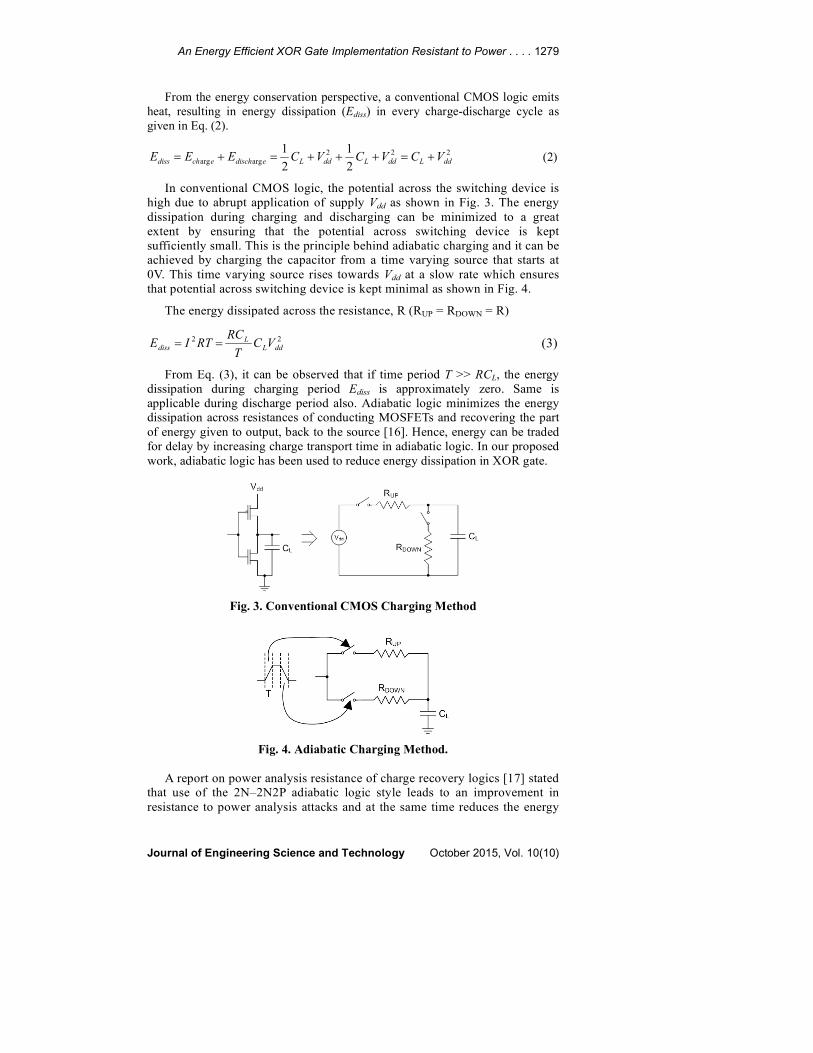
SABL Logic is based on strongARM110 Flip-flop (SAFF) [11]. It is a Dynamic
Logic and an XOR gate based on this logic is shown in Fig. 7. In this logic, XOR
function is achieved through DCVSL XOR pull down. The current drawn from
the power supply is maintained constant for any kind of input combinations by
using the bridging transistor M11. The bridging transistor M11 ensures that the
charges present in the internal capacitances are discharged to a zero value so that
the circuit consumes equal current irrespective of the input sequence. The SABL
logic is differential, dynamic and a clock signal is used to control different phases
of its operation such as evaluation and Precharge. However, the main drawback of
the SABL XOR gate is that it requires 14 transistors for its operation and it
consumes more energy due to its non-adiabatic nature.
Fig. 7. SABL XOR Gate.
4.2. Symmetric adiabatic logic (SyAL)
An Efficient Charge Recovery Logic (ECRL) based AND/NAND gate has been
proposed to resist power analysis attacks [12]. The constant current consumption
for all possible input combinations is achieved by assigning input data to the pull
down paths such that on- and off-transistors are configured equally for all discharge
paths. The charge sharing between the internal nodes is achieved by five bridging
transistors which are controlled by a separate control signal BR. These bridging
transistors are responsible for balancing the charges present in the internal nodes
N1, N2, N3, N4 and output nodes Out, Outbar after the recovery phase. As a result,
the current drawn from the power supply is not affected by the previous input data.
The symmetric adiabatic logic style implementation of AND/NAND gate requires
15 transistors as shown in Fig. 8. A Charge Sharing based Symmetric Adiabatic

1282 Saravanan P. and Kalpana P.
Journal of Engineering Science and Technology October 2015, Vol. 10(10)
Logic style (CSSAL) has been proposed for AND/NAND gate implementation
[13]. It has been claimed that just by adding two transistors at the output nodes of
the SyAL AND/NAND gate, resistance to power analysis attacks has been
improved. But when SyAL and CSSAL logic styles are used to design an XOR
gate, they require a minimum of three AND/NAND gates which leads to more
number of transistors for one XOR gate implementation. This results in higher area
overhead and also higher energy dissipation.
Fig. 8. SyAL AND/NAND Gate
5. Proposed Implementation of XOR Gate
In cryptography, XOR operation plays an important role in ciphering and
deciphering the data. The XOR operation when implemented with SABL consumes
more energy due to its non-adiabatic nature and with SyAL and CSSAL takes more
number of transistors. In order to overcome these drawbacks, a novel energy
efficient and power analysis attacks resistant XOR gate has been proposed in this
work. The proposed XOR/XNOR gate structure has DCVSL pull-down network
combined with adiabatic 2N-2N2P pull-up and a charge sharing mechanism to
achieve constant current consumption independent of the inputs.
5.1. DCVSL pull-down network
Among all the transistor level implementations, DCVSL uses minimum number
of transistors for XOR operation. Hence in our proposed implementation, DCVSL
pull-down network is employed which requires only six transistors (M1-M6) from
the DCVSL XOR gate implementation as shown in Fig. 2. Though the DVCSL
uses less number of transistors for XOR gate implementation, it is highly
vulnerable to power analysis attacks. This is mainly due to improper charge
sharing between the capacitances at its internal nodes and output nodes. Due to
this, the current plot varies for different input combinations as illustrated in Fig. 9.
Hence the attacker can easily predict the input pattern from the current traces of
the power supply of XOR gate. In order to circumvent this problem, adiabatic
pull-up is used in our proposed implementation.

An Energy Efficient XOR Gate Implementation Resistant to Power . . . . 1283
Journal of Engineering Science and Technology October 2015, Vol. 10(10)
Fig. 9. Supply Current Waveform of DCVSL XOR Gate
for Exhaustive Input Patterns.
5.2. 2N-2N2P adiabatic pull-up network
In 2N-2N2P adiabatic logic, the CMOS latch is responsible for keeping the output
nodes non-floating and also increases the power analysis resistance. Hence the
adiabatic CMOS latch is connected as pull-up network in our proposed XOR gate
implementation as shown in Fig. 10. After replacing the DCVSL pull-up network
with adiabatic pull-up network, the variations in the power supply current traces
are minimal for stable inputs. When sequence of inputs is applied, then the power
supply current traces are distinguishable as shown in Fig. 11. Hence the attacker
still has the option of deriving inputs from the current traces of power supply by
applying sequence of inputs. To avoid this dependency, charge sharing
mechanism is employed in our proposed implementation.
Fig. 10. Proposed XOR Gate with Adiabatic Pull-up Network.
1284 Saravanan P. and Kalpana P.
Journal of Engineering Science and Technology October 2015, Vol. 10(10)
Fig. 11. Supply Current Waveform of Proposed XOR Gate
for Sequence of Input Patterns.
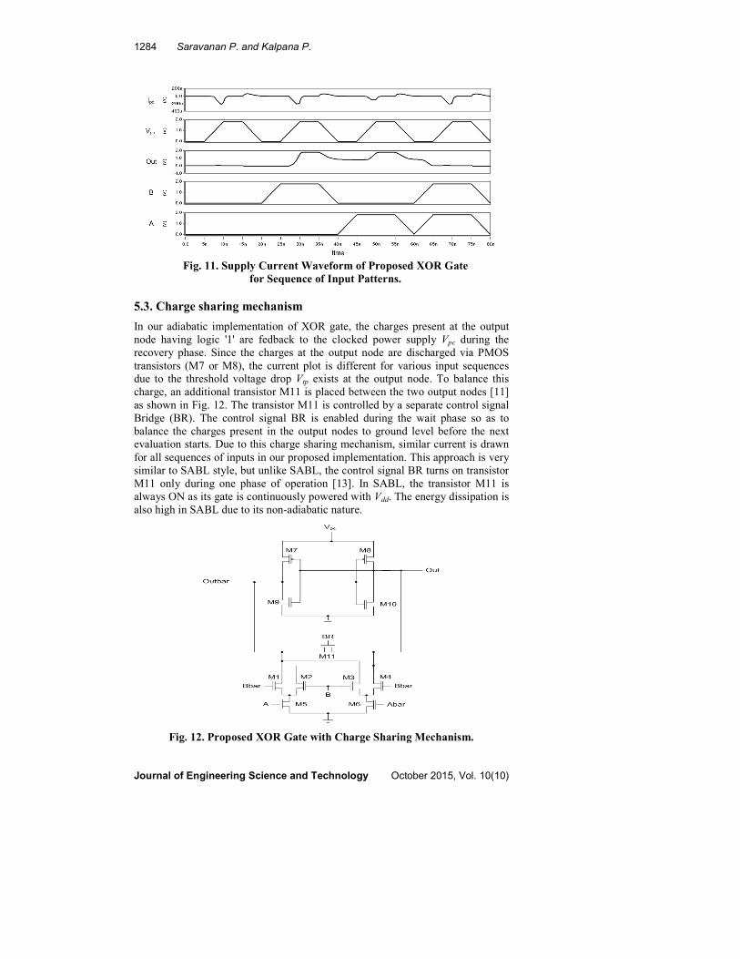
5.3. Charge sharing mechanism
In our adiabatic implementation of XOR gate, the charges present at the output
node having logic '1' are fedback to the clocked power supply Vpc during the
recovery phase. Since the charges at the output node are discharged via PMOS
transistors (M7 or M8), the current plot is different for various input sequences
due to the threshold voltage drop Vtp exists at the output node. To balance this
charge, an additional transistor M11 is placed between the two output nodes [11]
as shown in Fig. 12. The transistor M11 is controlled by a separate control signal
Bridge (BR). The control signal BR is enabled during the wait phase so as to
balance the charges present in the output nodes to ground level before the next
evaluation starts. Due to this charge sharing mechanism, similar current is drawn
for all sequences of inputs in our proposed implementation. This approach is very
similar to SABL style, but unlike SABL, the control signal BR turns on transistor
M11 only during one phase of operation [13]. In SABL, the transistor M11 is
always ON as its gate is continuously powered with Vdd. The energy dissipation is
also high in SABL due to its non-adiabatic nature.
Fig. 12. Proposed XOR Gate with Charge Sharing Mechanism.

An Energy Efficient XOR Gate Implementation Resistant to Power . . . . 1285
Journal of Engineering Science and Technology October 2015, Vol. 10(10)
5.4. Operation of proposed XOR gate
The proposed XOR gate operation depends on the proper sequence of input
signals as shown in Fig. 13. The timing diagram has four phases of operation [13]
such as wait/bridge, evaluate, hold, recovery and all these four phases should be
executed in a sequence. The proposed XOR gate inputs A, Abar, B and Bbar
should be applied during the wait phase because during this phase, the clocked
power supply (Vpc) will have zero voltage. At the same time, the control signal
BR should be enabled in this phase to balance the charges present in all internal
node capacitances. The applied inputs will be evaluated during the evaluate phase
where the clocked power supply (Vpc) raises from 0 to its peak value of 1.8V. The
evaluated XOR outputs are available during hold phase where the power clock is
stable at 1.8 V. After the evaluation phase the charges present at the output nodes
will be fedback to the power clock during the recovery phase.
The Equivalent Resistance-Capacitance (RC) models of the proposed XOR
gate during Evaluation phase is shown in Fig. 14. When a transistor in the pull-
down network is turned on, then it can be represented by its corresponding ON
channel resistance R in the RC model. The internal node capacitance is
represented as C. From Fig. 14, it can be observed that equal number of
capacitors is charged during the evaluation phase for all possible input
combinations in our proposed XOR gate. During the wait/bridge phase, the
charges present in the internal nodes and output nodes are properly shared
through transistor M11 as illustrated in Fig. 15. Since equal number of capacitors
is charged during Evaluation phase and all the charges present at the internal and
output nodes are properly shared during Bridge phase, the current traces will be
identical for all exhaustive input combinations in our proposed XOR gate. The
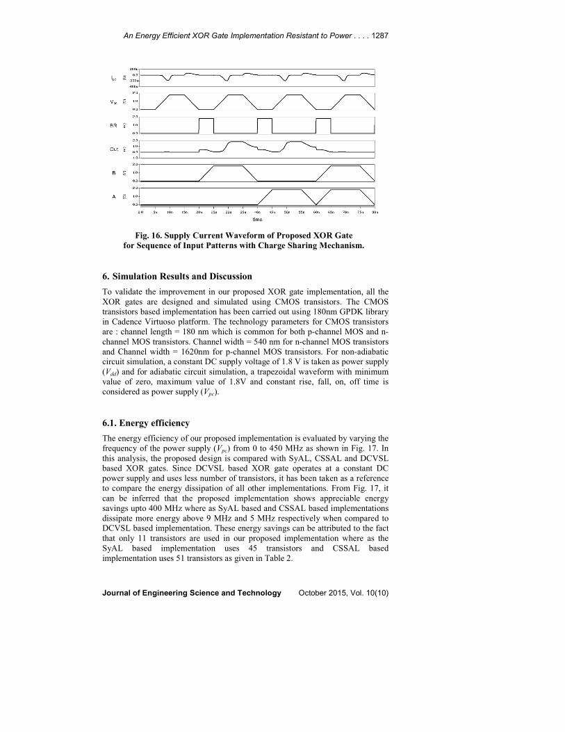
simulation waveform of proposed XOR gate is shown in Fig. 16 where it can be
observed that stable output is available during hold phase.
Fig. 13. Timing Diagram of Proposed XOR Gate.

1286 Saravanan P. and Kalpana P.
Journal of Engineering Science and Technology October 2015, Vol. 10(10)
Fig. 14. Equivalent RC Models of Proposed
XOR Gate during Evaluation Phase.
Fig. 15. Equivalent RC Models of Proposed XOR Gate during Bridge Phase.
An Energy Efficient XOR Gate Implementation Resistant to Power . . . . 1287
Journal of Engineering Science and Technology October 2015, Vol. 10(10)
Fig. 16. Supply Current Waveform of Proposed XOR Gate
for Sequence of Input Patterns with Charge Sharing Mechanism.
6. Simulation Results and Discussion
To validate the improvement in our proposed XOR gate implementation, all the
XOR gates are designed and simulated using CMOS transistors. The CMOS
transistors based implementation has been carried out using 180nm GPDK library
in Cadence Virtuoso platform. The technology parameters for CMOS transistors
are : channel length = 180 nm which is common for both p-channel MOS and n-
channel MOS transistors. Channel width = 540 nm for n-channel MOS transistors
and Channel width = 1620nm for p-channel MOS transistors. For non-adiabatic
circuit simulation, a constant DC supply voltage of 1.8 V is taken as power supply
(Vdd) and for adiabatic circuit simulation, a trapezoidal waveform with minimum
value of zero, maximum value of 1.8V and constant rise, fall, on, off time is
considered as power supply (Vpc).
6.1. Energy efficiency
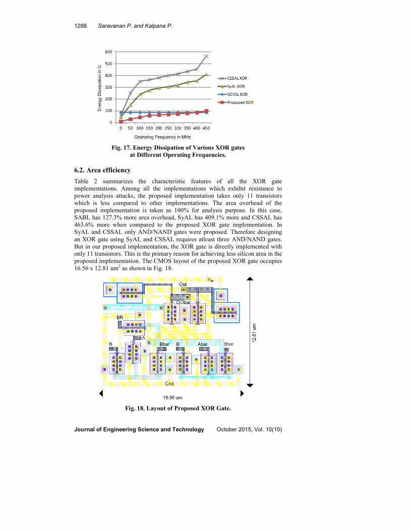
The energy efficiency of our proposed implementation is evaluated by varying the
frequency of the power supply (Vpc) from 0 to 450 MHz as shown in Fig. 17. In
this analysis, the proposed design is compared with SyAL, CSSAL and DCVSL
based XOR gates. Since DCVSL based XOR gate operates at a constant DC
power supply and uses less number of transistors, it has been taken as a reference
to compare the energy dissipation of all other implementations. From Fig. 17, it
can be inferred that the proposed implementation shows appreciable energy
savings upto 400 MHz where as SyAL based and CSSAL based implementations
dissipate more energy above 9 MHz and 5 MHz respectively when compared to
DCVSL based implementation. These energy savings can be attributed to the fact
that only 11 transistors are used in our proposed implementation where as the
SyAL based implementation uses 45 transistors and CSSAL based
implementation uses 51 transistors as given in Table 2.
1288 Saravanan P. and Kalpana P.
Journal of Engineering Science and Technology October 2015, Vol. 10(10)
Fig. 17. Energy Dissipation of Various XOR gates
at Different Operating Frequencies.
6.2. Area efficiency
Table 2 summarizes the characteristic features of all the XOR gate
implementations. Among all the implementations which exhibit resistance to
power analysis attacks, the proposed implementation takes only 11 transistors
which is less compared to other implementations. The area overhead of the
proposed implementation is taken as 100% for analysis purpose. In this case,
SABL has 127.3% more area overhead, SyAL has 409.1% more and CSSAL has
463.6% more when compared to the proposed XOR gate implementation. In
SyAL and CSSAL only AND/NAND gates were proposed. Therefore designing
an XOR gate using SyAL and CSSAL requires atleast three AND/NAND gates.
But in our proposed implementation, the XOR gate is directly implemented with
only 11 transistors. This is the primary reason for achieving less silicon area in the
proposed implementation. The CMOS layout of the proposed XOR gate occupies
16.56 x 12.81 um2 as shown in Fig. 18.
Fig. 18. Layout of Proposed XOR Gate.

An Energy Efficient XOR Gate Implementation Resistant to Power . . . . 1289
Journal of Engineering Science and Technology October 2015, Vol. 10(10)
Table 2. Characteristic Features of Different XOR Gates.
Type of
Implementation
Energy
Saving
Mode
Power
Analysis
Resistance
No. of
Transistors
Area
Overhead
in %
Conventional
CMOS
Non-Adiabatic
No 14 127.3
DCVSL Non-
Adiabatic
No 8 72.7
SABL [11] Non-
Adiabatic
Yes 14 127.3
SyAL [12] Adiabatic Yes 45 409.1
CSSAL [13] Adiabatic Yes 51 463.6
Proposed Adiabatic Yes 11 100
6.3. Measure of resistance to power analysis attacks
To evaluate the resistance against power analysis attacks, two parameters
Normalized Energy Deviation (NED) and Normalized Standard Deviation (NSD)
are considered [4]. The parameter NED is defined as the percentage difference
between the maximum energy consumption (Emax) and minimum energy
consumption (Emin) over all possible input combinations and transitions as shown
in Eq. (4). The parameter NSD indicates how much the energy consumption
varies based on the inputs as shown in Eq. (5). Ideally these two parameters NED
and NSD should approach zero for better resistance to power analysis attacks.
max
minmax
E
EENED
−= (4)
avg
E
ENSD
σ= (5)
where
( )∑ −=i
avgiE nEE /2
σ (6)
and
minmax EEEavg −= (7)
Fig. 19. Normalized Energy Deviation at Different Operating Frequencies.

1290 Saravanan P. and Kalpana P.
Journal of Engineering Science and Technology October 2015, Vol. 10(10)
Table 3 shows the performance improvement of our proposed implementation
in comparison to existing SyAL and CSSAL based XOR gates. The NED and
NSD analyses have been carried out for four random frequencies 1 MHz, 1.25
MHz, 2 MHz and 5 MHz. It can be observed that our proposed implementation
shows 20.8%, 13.6% reduction in NED and 26.1%, 19.1% in NSD when
compared to SyAL and CSSAL based XOR gates as shown Figs. 19 and 20
respectively. This is mainly due to the 2N-2N2P adiabatic pull-up, addition of
charge sharing mechanism through transistor M11 and usage of less number of
transistors in the proposed XOR gate implementation. Also the proposed
implementation shows 79.6% and 82.5% savings in energy at an operating
frequency of 5 MHz when compared to SyAL and CSSAL based XOR gates.
Fig. 20. Normalized Standard Deviation at Different Operating Frequencies.
Table 3. Performance Analysis of Different XOR Gates.
Para-
meters
SyAL XOR
[12]
CSSAL XOR
[13] Proposed XOR
1
MHz
1.25
MHz
2
MHz
5
MHz
1
MHz
1.25
MHz
2
MHz
5
MHz
1
MHz
1.25
MHz
2
MHz
5
MHz
Eavg (fJ) 48.43 50.89 55.29 71.64 57.85 61.25 63.27 83.7 9.53 9.83 10.94 14.61
σσσσE 0.12 0.3 0.45 0.3 0.227 0.89 0.26 0.38 0.018 0.041 0.048 0.049
NED
(×10-3)
15 14 19.4 11 15.6 012 19 12 10.3 11 11.8 9.5
NSD
(×10-3)
2.4 5.9 8.3 4.2 3.9 14.6 17 4.6 1.8 4.3 4.3 3.4
7. Conclusions
An energy efficient and power analysis attacks resistant XOR gate which
consumes constant current for all possible input combinations has been proposed
in this work. The proposed XOR gate saves 79.6% and 82.5% energy compared
to SyAL and CSSAL XOR gates respectively. It also shows 20.8%, 13.6%
reduction in NED and 26.1%, 19.1% reduction in NSD when compared to SyAL
and CSSAL XOR gates respectively. In addition, the proposed XOR gate
implementation shows 409.1% and 463.6% less area overhead when compared to
the SyAL XOR gate and CSSAL XOR gate respectively. The CMOS layout of
proposed XOR gate has been drawn which occupies 16.56 x 12.81 um2. Hence
the proposed XOR gate can be used to implement any energy efficient secure
hardware to avoid power analysis attacks.

An Energy Efficient XOR Gate Implementation Resistant to Power . . . . 1291
Journal of Engineering Science and Technology October 2015, Vol. 10(10)
References
1. Kocher, P.; Jaffe, J.; and Jun, B. (1999). Differential Power Analysis.
Proceedings of Advances in Cryptology-CRYPTO'99. California, USA,
388-397.
2. Moradi, A.; Mohammad Taghi Manzuri Shalmani; and Mahmoud
Salmasizadeh. (2009). Dual-rail transition logic: A logic style for
counteracting power analysis attacks. Computers & Electrical Engineering,
35(2), 359–369.
3. Moradi, A.; Eisenbarth, T.; Poschmann, A.; and Paar, C. (2010). Power
analysis of single-rail storage elements as used in MDPL. Proceedings of
Information Security and Cryptology-ICISC 2009. Seoul, Korea, 146–160.
4. Marco Bucci; Luca Giancane; Raimondo Lazzi; and Alessandro Trifiletti.
(2006). Three-Phase Dual-Rail Pre-charge Logic. Proceedings of
Cryptographic Hardware And Embedded Systems-CHES 2006. Yokohama,
Japan, 232-241.
5. Allam, M.W.; and Elmasry, M.I. (2001). Dynamic current mode logic
(DyCML): A new low-power high-performance logic style. IEEE Journal of
Solid-State Circuits, 36(3), 550-558.
6. Muresan, R.; and Gregori, S. (2008). Protection circuit against differential
power analysis attacks for smart cards. IEEE Transactions on Computers,
57(11), 1540-1549.
7. Ratanpal, G.B.; Williams, R.D.; and Blalock, T.N. (2004). An on-chip signal
suppression countermeasure to power analysis attacks. IEEE Transactions on
Dependable and Secure Computing, 1(3), 179-189.
8. Ramakrishnan, L.N.; Chakkaravarthy, M.; Manchanda, A.S.; and
Borowczak, M. (2012). SDMLp: On the use of complementary Pass
transistor Logic for design of DPA resistant circuits. IEEE International
Symposium on Hardware-Oriented Security and Trust-HOST 2012. San
Francisco, CA, 31-36.
9. Tiri, K.; and Verbauwhede, I. (2004). A logic level design methodology for a
secure DPA resistant ASIC or FPGA implementation. Proceedings of the
conference on Design, automation and Test in Europe. Paris, France, 246-251.
10. Tiri, K.; and Verbauwhede, I. (2004). Charge recycling sense amplifier based
logic: securing low power security IC’s against DPA. Proceedings of the 30th
European Conference on Solid-State Circuits-ESSCIRC 2004. Leuven,
Belgium, 179–182.
11. Tiri, K.; Akmal, M.; and Verbauwhede, I. (2002). A dynamic and differential
CMOS logic with signal independent power consumption to withstand
differential power analysis on smart cards. Proceedings of the 28th European
Conference on Solid-State Circuits-ESSCIRC 2002. Firenze, Italy, 403–406.
12. Choi, B.D.; Kim, K.E.; Chung, K.S.; and Kim, D.K. (2010). Symmetric
adiabatic logic circuits against differential power analysis. ETRI journal,
32(1), 166-168.
13. Monteiro, C.; Takahashi, Y.; and Sekine, T. (2013). Charge-sharing
symmetric adiabatic logic in countermeasure against power analysis attacks
at cell level. Microelectronics Journal, 44(6), 496-503.

1292 Saravanan P. and Kalpana P.
Journal of Engineering Science and Technology October 2015, Vol. 10(10)
14. Rabaey, J.M.; Anantha Chandrakasan; and Borivoje Nikolic. (1996). Digital
integrated circuits : A Design Perspective (2nd
ed.). New York: Prentice Hall.
15. Heller, L.; Griffin, W.; Davis, J.; and Thoma, N. (1984). Cascode voltage
switch logic: A differential CMOS logic family. IEEE International
Conference on Solid-State Circuits. San Francisco, CA, 16-17.
16. Athas, W.C.; Svesson, L.J.; Koller, J.G.; Traztzanis, N.; and Chuo, E.Y.
(1994). Low power digital system based on adiabatic-switching principles.
IEEE Transactions on VLSI Systems, 2(4), 398–407.
17. Moradi, A.; Khatir, M.; Salmasizadeh, M.; and Shalmani, M.TM. (2008).
Investigating the DPA-resistance property of charge recovery logics. IACR
Cryptology ePrint Archive, 192.
18. Kramer, A.; Denker, J.S.; Flower, B.; and Moroney, J. (1995). 2nd order
adiabatic computation with 2N-2P and 2N-2N2P logic circuits. Proceedings of
the International Symposium on Low power design. California, USA, 191-196.