Low Power Three Input XOR Gate For Arithmetic And Logical … · 2018-01-03 · required. The...
6
© 2017 IJSRET 222 International Journal of Scientific Research & Engineering Trends Volume 3, Issue 6, Nov.-2017, ISSN (Online): 2395-566X Low Power Three Input XOR Gate For Arithmetic And Logical Operation Ms. Pooja Sahu Dept. of Electronic and Communication IES College of Technology, Bhopal, India [email protected] Mr. Ashish Raghuwanshi Dept. of Electronic and Communication IES College of Technology, Bhopal, India Abstract – With advancement of microelectronics technology scaling, the main objective of design i.e. low power consumption can be easily acquired. For any digital logic design the power consumption depends on; Supply voltage, number of transistors incorporated in circuit and scaling ratios of the same. As CMOS technology supports inversion logic designs; NAND & NOR structures are useful for converting any logic equation into physical level design that comprises of PMOS and NMOS transistors. In similar way, logic can be implemented in other styles as well, with the difference in number of transistors required. The conventional CMOS design for three input XOR logic can be possible with 10 or more than 10 transistors, with the methodology discussed in this paper, the same design for three inputs XOR logic can be made possible with 16 transistors. The proposed methodology consists of transmission gate and systematic cell design methodology (SCDM). This design consumes 45% (35%) less power dissipation than that of conventional LPHS-FA and SCDM based XO10 XOR logic design with CMOS technology. Since the design for XOR logic, is useful for variety of applications such as Data encryption, Arithmetic circuits, Binary to Gray encoding etc. the XOR logic has been selected for design. The design explained in this paper is simulated with 130nm technology. Keywords – Adders, Transistors, Delay, CMOS integrated circuits, Logic gates, Hybrid adder, XOR, Full adders, VLSI circuit. I. INTRODUCTION In last few decades, the increase in processing speed and exponential scaling in feature size has been successfully attained using lithography based VLSI technology. But this trend faces some serious challenges because of basic limits of CMOS technology such as short channel effects. A XOR gate is one of the imperative building bricks of in the formation of a arithmetic and logic unit of embedded system [1-6]. With technology scaling, power consumption has turned out to be the most crucial concern of all design constraints in recent years [7-11]. In the past, processor speed, circuit speed, area, performance, cost and reliability were of primary interest while power consumption was attributed a secondary concern. However, with escalating eminence in portable and wireless communications systems, power consumption is being given equal importance in prevailing time. High performance processors consume intense power which consequently increases the cost related with packaging and cooling. Moreover, high power systems frequently run hot increasing the temperature thus having a tendency to aggravate various Silicon failure approaches such as electromigration, thermal runaway, decrement in transconductance, junction diffusion, threshold voltage shift, electrical parameter shift, electrostatic discharge (ESD), package related failure, electrical over-stress (EOS) and silicon interconnect failure [12]. It has been determined every 10 0 upsurge in temperature nearly doubles the failure rate thereby disturbing the reliability. In this perspective, peak power consumption is a vital design issue because it resolves the thermal as well as electrical confines of designs, influences the system cost, size, weight, and prescribes the battery type, constituent in conjunction with system packaging and heat sinks. Additionally, peak power consumption exacerbates the resistive and inductive voltage drop tribulations. From the biological point of vision, meagre heat will be propelled into rooms provided power dissipation of electronic systems is abridged. Also, fewer electricity will be consumed which as an upshot will have an assenting effect on the global environment. The XOR gate is one of the most important components of arithmetic and logic unit used in microprocessor. This plays an important role in SoC (silicon on chip) to design ALU in small die area that reduce manufacturing cost. This system inbuilt ALU occupy more area on silicon chip that dissipate more heat and elevate the temperature of chip. This thing degrades the performance of system. In order to save the chip heat sink is needed that release the internal heat to external environment. As the operating frequency of dynamic XOR improves, dynamic power consumption becomes dominant that introduce heating problem as mentioned above. To overcome this problem, dynamic XOR gate proposed with minimum delay and smaller power consumption. The rest of this brief is organized as follows. Previous work is discussed in Section II. The details of proposed
Transcript of Low Power Three Input XOR Gate For Arithmetic And Logical … · 2018-01-03 · required. The...
© 2017 IJSRET
222
International Journal of Scientific Research & Engineering Trends Volume 3, Issue 6, Nov.-2017, ISSN (Online): 2395-566X
Low Power Three Input XOR Gate For Arithmetic And
Logical Operation
Ms. Pooja Sahu
Dept. of Electronic and Communication
IES College of Technology,
Bhopal, India
Mr. Ashish Raghuwanshi Dept. of Electronic and Communication
IES College of Technology,
Bhopal, India
Abstract – With advancement of microelectronics technology scaling, the main objective of design i.e. low power consumption
can be easily acquired. For any digital logic design the power consumption depends on; Supply voltage, number of transistors
incorporated in circuit and scaling ratios of the same. As CMOS technology supports inversion logic designs; NAND & NOR
structures are useful for converting any logic equation into physical level design that comprises of PMOS and NMOS
transistors. In similar way, logic can be implemented in other styles as well, with the difference in number of transistors
required. The conventional CMOS design for three input XOR logic can be possible with 10 or more than 10 transistors, with
the methodology discussed in this paper, the same design for three inputs XOR logic can be made possible with 16 transistors.
The proposed methodology consists of transmission gate and systematic cell design methodology (SCDM). This design consumes
45% (35%) less power dissipation than that of conventional LPHS-FA and SCDM based XO10 XOR logic design with CMOS
technology. Since the design for XOR logic, is useful for variety of applications such as Data encryption, Arithmetic circuits,
Binary to Gray encoding etc. the XOR logic has been selected for design. The design explained in this paper is simulated with
130nm technology.
Keywords – Adders, Transistors, Delay, CMOS integrated circuits, Logic gates, Hybrid adder, XOR, Full adders, VLSI
circuit.
I. INTRODUCTION
In last few decades, the increase in processing speed and
exponential scaling in feature size has been successfully
attained using lithography based VLSI technology. But this
trend faces some serious challenges because of basic limits
of CMOS technology such as short channel effects. A
XOR gate is one of the imperative building bricks of in the
formation of a arithmetic and logic unit of embedded
system [1-6]. With technology scaling, power consumption
has turned out to be the most crucial concern of all design
constraints in recent years [7-11]. In the past, processor
speed, circuit speed, area, performance, cost and reliability
were of primary interest while power consumption was
attributed a secondary concern. However, with escalating
eminence in portable and wireless communications
systems, power consumption is being given equal
importance in prevailing time. High performance
processors consume intense power which consequently
increases the cost related with packaging and cooling.
Moreover, high power systems frequently run hot
increasing the temperature thus having a tendency to
aggravate various Silicon failure approaches such as
electromigration, thermal runaway, decrement in
transconductance, junction diffusion, threshold voltage
shift, electrical parameter shift, electrostatic discharge
(ESD), package related failure, electrical over-stress
(EOS) and silicon interconnect failure [12]. It has been
determined every 100 upsurge in temperature nearly
doubles the failure rate thereby disturbing the reliability. In
this perspective, peak power consumption is a vital design
issue because it resolves the thermal as well as electrical
confines of designs, influences the system cost, size,
weight, and prescribes the battery type, constituent in
conjunction with system packaging and heat sinks.
Additionally, peak power consumption exacerbates the
resistive and inductive voltage drop tribulations. From the
biological point of vision, meagre heat will be propelled
into rooms provided power dissipation of electronic
systems is abridged. Also, fewer electricity will be
consumed which as an upshot will have an assenting effect
on the global environment. The XOR gate is one of the
most important components of arithmetic and logic unit
used in microprocessor. This plays an important role in
SoC (silicon on chip) to design ALU in small die area that
reduce manufacturing cost. This system inbuilt ALU
occupy more area on silicon chip that dissipate more heat
and elevate the temperature of chip. This thing degrades
the performance of system. In order to save the chip heat
sink is needed that release the internal heat to external
environment. As the operating frequency of dynamic XOR
improves, dynamic power consumption becomes dominant
that introduce heating problem as mentioned above. To
overcome this problem, dynamic XOR gate proposed with
minimum delay and smaller power consumption.
The rest of this brief is organized as follows. Previous
work is discussed in Section II. The details of proposed

© 2017 IJSRET
223
International Journal of Scientific Research & Engineering Trends Volume 3, Issue 6, Nov.-2017, ISSN (Online): 2395-566X
SCDM based three-input XOR is discussed in Section III.
Simulation results are analyzed in Section IV. Finally, the
conclusions are drawn in Section V.
II. PREVIOUS WORK
LPHS-FA stands for low power and high speed full
adder, which is based on hybrid logic. LPHS-FA[13]
schematic shown in Fig. 1, demonstrates low-power and
high-speed advantages, and merely requires 15 MOSFETs
to implement.
Fig. 1 Circuit schematic of LPHS-FA[13]
The transmission-gates CMOS adder (TG-CMOS)[14],
it is based on transmission gates and has 20 transistors. It
consumes more power. Next is 18TnewFA[15] is based on
18T and consumes more power.
Work on SCDM based XOR gate can be divided into two
categories as they are extracted from the topic: 1)
traditional three input XOR gate and 2) its operating
methodologies. Cell design methodology has been
presented to design some limited functions, such as two-
input XOR/XNOR and carry–inverse carry in the hybrid-
CMOS style [16-18]. The predominant results persuade us
to improve CDM through two stages: 1) generating more
complex functions and 2) rectifying some remaining flaws.
The flaws in previously published CDM include
containing some manual steps in the design flow and
generating a large number of designs in which the
predominant ones would be determined after the
completion of simulations. Therefore, in the first stage, a
three-input XOR/XNOR as one of the most complex and
all-purpose three-input basic gates in arithmetic circuits
have been chosen. If the efficiency of the circuits is
confirmed in such a competitive environment, it can show
the strength of the methodology. In the second stage, CDM
is matured as systematic CDM (SCDM) in designing the
three-input XOR/XNORs for the first time. It
systematically generates elementary basic cell (EBC) using
binary decision diagram (BDD), and wisely chooses circuit
components based on a specific target. This takes place
when the mentioned features are not considered in the
CDM. Therefore, after the systematic generation, the
SCDM considers circuit optimization based on our target
in three steps: 1) wise selection of the basic cell; 2) wise
selection of the amend mechanisms; and 3) transistor
sizing. It should be noted that BDD can be utilized for
EBC generation of other three-input functions. We
consider the power-delay product (PDP) as the design
target. It stands as a fair performance metric, precisely
involving portable electronic system targets. The
motivation to use this methodology is the presence of some
unique features and the ability to produce some efficient
circuits that enjoy all these advantages.
The SCDM divides a circuit structure into a main structure
and optimization-correction mechanisms. In the main
structure, it considers features including the least number
of transistors in critical path, fairly balanced outputs, being
power ground- free, and symmetry. The mechanisms have
the duty of completing the functionality of the circuits,
avoiding any degradation on the output voltage, and
increasing the driving capability.
The dynamic consumption optimization comes from the
fact of well-balanced propagation delay. This feature is
advantageous for applications in which the skew between
arriving signals is critical for proper operation, and for
cascaded applications to reduce the chance of making
glitches [2]. Power-ground-free main structure leads to
power reduction.
The degradation in all output voltage swing can thus be
completely removed, which makes the design sustainable
in low VDD operations and low static power dissipation.
The methodology has high flexibility in target and
systematically considers it in the three design steps. This
can lead to efficient circuits in terms of performance,
power, power delay product (PDP), energy delay
product(EDP), layout area.
The fast evolution of microelectronics fabrication
processes demands a new cell library generation or a
library technology migration. The well-organized
systematic methodology leads to automated flow, which
can reduce design time and costs, provide consistency in
the cell library generation process, increase the range of
simulation capabilities at the characteristics step, as well as
minimize the risk of errors [17, 19]. Recently published
article on hybrid type systematic cell design methodology
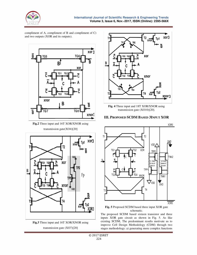
(SCDM) applied on three circuit as shown in Fig.2, Fig.3
and Fig..4. all three circuit have six inputs (A, B, C,
© 2017 IJSRET
224
International Journal of Scientific Research & Engineering Trends Volume 3, Issue 6, Nov.-2017, ISSN (Online): 2395-566X
compliment of A, compliment of B and compliment of C)
and two outputs (XOR and its outputs).
Fig.2 Three input and 16T XOR/XNOR using
transmission gate(XO4)[20]
Fig.3 Three input and 16T XOR/XNOR using
transmission gate (XO7)[20]
Fig. 4 Three input and 18T XOR/XNOR using
transmission gate (XO10)[20].
III. PROPOSED SCDM BASED 3INPUT XOR
Fig. 5 Proposed SCDM based three input XOR gate
schematic.
The proposed SCDM based sixteen transistor and three
inputs XOR gate circuit as shown in Fig. 5. As like
existing SCDM, The predominant results motivate us to
improve Cell Design Methodology (CDM) through two
stages methodology: a) generating more complex functions
© 2017 IJSRET
225
International Journal of Scientific Research & Engineering Trends Volume 3, Issue 6, Nov.-2017, ISSN (Online): 2395-566X
minterms and b) rectifying some remaining repetitive
minterms. In this cell, two full swing generator pair is
added between node XOR3 and its compliment using four
transistors TPP1, TPP2, TNN1 and TNN2. The proposed
cell offers smaller delay and power consumption by
eliminating transistors Tp1 and Tp2 from SCDM based
exiting XOR gates XO7 and XO10. Proposed technique
offers smaller propagation delay, power dissipation and
power delay product than LPHSFA, TF, 18TnewFS, XO4,
XO7 and XO10.
IV. SIMULATION RESULTS AND
COMPARISON
To evaluate the performance of XOR/XNOR gate, it is
necessary to study the timing analysis of proposed design
under similar technology and supply voltage with different
design. We have performed complete study using Hspice
EDA Tool [21]. To investigate and compare the
performance of different XOR gate such as LPHSFA, TF,
18TnewFS, XO4, XO7 and XO10, whose excellence have
been confirmed in [13] [22] and [4, 23, 24]. Therefore, an
approximately fair comparison will take place by selecting
them. Table-1 presents that proposed design shows
superior performance than LPHSFA, TF, 18TnewFS,
XO4, XO7 and XO10. While normalized comparison of
design parameters are shown in Fig. 6, Fig. 7, Fig. 8 and
Fig. 9.
Table-1: Comparison of different design parameter results
at 130nm technology[25]
CIRCUI
TS
PDP
(FJ)
POWER
CONSUMPT
ION
(µW)
PROPAG
ATION
DELAY
(NS)
NO. OF
TRANSI
STORS
USED
LPHS-
FA
0.91 3.41 0.38 14
TF 0.52 2.79 0.23 20
18TNE
WFS
0.52 2.75 0.24 18
XO4 0.42 3.07 0.22 16
XO7 0.47 3.17 0.19 16
XO10 0.50 2.99 0.19 18
PROPOS
ED
0.1244 1.9289 0.0645 16
Fig. 6 Normalized comparison of delay
Fig. 7 Normalized comparison of power dissipation

© 2017 IJSRET
226
International Journal of Scientific Research & Engineering Trends Volume 3, Issue 6, Nov.-2017, ISSN (Online): 2395-566X
Fig. 8 Normalized comparison of power delay product
Fig. 9 Normalized comparison of area overhead
V. CONCLUSION
The MOSFET based three inputs XOR gates are
extensively employed in portable modern high
performance data processing units because of high speed
and controllable evaluation by clock node, but they suffer
from high power consumption and input signal skew.
Proposed SCDM based three inputs XOR gate offers
smaller propagation delay, power dissipation and
propagation delay than LPHSFA, TF, 18TnewFS, XO4,
XO7 and XO10. The proposed design consumes 45%
(35%) less power dissipation than that of conventional
LPHS-FA and SCDM based XO10 XOR logic design with
CMOS technology.
REFERENCES
[1]. B. Stackhouse, S. Bhimji, C. Bostak, D. Bradley, B.
Cherkauer, J. Desai, et al., "A 65 nm 2-billion
transistor quad-core itanium processor," IEEE Journal
of Solid-State Circuits, vol. 44, pp. 18-31, 2009.
[2]. H. Kaul, M. A. Anders, S. K. Mathew, S. K. Hsu, A.
Agarwal, R. K. Krishnamurthy, et al., "A 320 mv 56
µw 411 gops/watt ultra-low voltage motion estimation
accelerator in 65 nm cmos," IEEE Journal of Solid-
State Circuits, vol. 44, pp. 107-114, 2009.
[3]. Y.-H. Shu, S. Tenqchen, M.-C. Sun, and W.-S. Feng,
"XNOR-based double-edge-triggered flip-flop for two-
phase pipelines," IEEE Transactions on Circuits and
Systems II: Express Briefs, vol. 53, pp. 138-142, 2006.
[4]. S. Goel, M. A. Elgamel, M. A. Bayoumi, and Y.
Hanafy, "Design methodologies for high-performance
noise-tolerant XOR-XNOR circuits," IEEE
Transactions on Circuits and Systems I: Regular
Papers, vol. 53, pp. 867-878, 2006.
[5]. Y. Leblebici, CMOS digital integrated circuits:
analysis and design: McGraw-Hill College, 1996.
[6]. N. H. Weste and D. Harris, CMOS VLSI design: a
circuits and systems perspective: Pearson Education
India, 2015.
[7]. A. P. Chandrakasan and R. W. Brodersen,
"Minimizing power consumption in digital CMOS
circuits," Proceedings of the IEEE, vol. 83, pp. 498-
523, 1995.
[8]. A. P. Chandrakasan, S. Sheng, and R. W. Brodersen,
"Low-power CMOS digital design," IEICE
Transactions on Electronics, vol. 75, pp. 371-382,
1992.
[9]. K. Roy and S. C. Prasad, Low-power CMOS VLSI
circuit design: John Wiley & Sons, 2009.
[10]. J. Rabaey, Low power design essentials: Springer
Science & Business Media, 2009.
[11]. B. H. Calhoun, Y. Cao, X. Li, K. Mai, L. T. Pileggi, R.
A. Rutenbar, et al., "Digital circuit design challenges
and opportunities in the era of nanoscale CMOS,"
Proceedings of the IEEE, vol. 96, pp. 343-365, 2008.
[12]. C. H. Small, "Shrinking devices put the squeeze on
system packaging," EDN, vol. 39, pp. 41-54, 1994.
[13]. C.-K. Tung, S.-H. Shieh, and C.-H. Cheng, "Low-
power high-speed full adder for portable electronic
applications," Electronics Letters, vol. 49, pp. 1063-
1064, 2013.
[14]. A. M. Shams, T. K. Darwish, and M. A. Bayoumi,
"Performance analysis of low-power 1-bit CMOS full
adder cells," IEEE transactions on very large scale
integration (VLSI) systems, vol. 10, pp. 20-29, 2002.
© 2017 IJSRET
227
International Journal of Scientific Research & Engineering Trends Volume 3, Issue 6, Nov.-2017, ISSN (Online): 2395-566X
[15]. M. H. Moaiyeri, R. Faghih Mirzaee, K. Navi, T.
Nikoubin, and O. Kavehei, "Novel direct designs for 3-
input XOR function for low-power and high-speed
applications," International Journal of Electronics,
vol. 97, pp. 647-662, 2010.
[16]. D. Radhakrishnan, "Low-voltage low-power CMOS
full adder," IEE Proceedings-Circuits, Devices and
Systems, vol. 148, pp. 19-24, 2001.
[17]. H. T. Bui, A. K. Al-Sheraidah, and Y. Wang, "New 4-
transistor XOR and XNOR designs," in ASICs, 2000.
AP-ASIC 2000. Proceedings of the Second IEEE Asia
Pacific Conference on, 2000, pp. 25-28.
[18]. N. Gong, B. Guo, J. Lou, and J. Wang, "Analysis and
optimization of leakage current characteristics in sub-
65nm dual V t footed domino circuits,"
Microelectronics Journal, vol. 39, pp. 1149-1155,
2008.
[19]. J.-M. Wang, S.-C. Fang, and W.-S. Feng, "New
efficient designs for XOR and XNOR functions on the
transistor level," IEEE Journal of solid-state Circuits,
vol. 29, pp. 780-786, 1994.
[20]. T. Nikoubin, M. Grailoo, and C. Li, "Energy and Area
Efficient Three-Input XOR/XNORs With Systematic
Cell Design Methodology," IEEE Transactions on
Very Large Scale Integration (VLSI) Systems, vol. 24,
pp. 398-402, 2016.
[21]. [21] A. Eshra and A. El-Sayed, "An odd parity checker
prototype using DNAzyme finite state machine,"
IEEE/ACM Transactions on Computational Biology
and Bioinformatics, vol. 11, pp. 316-324, 2014.
[22]. [22] M. Aguirre-Hernandez and M. Linares-Aranda,
"CMOS full-adders for energy-efficient arithmetic
applications," IEEE transactions on very large scale
integration (VLSI) systems, vol. 19, pp. 718-721, 2011.
[23]. [23] S. Goel, A. Kumar, and M. A. Bayoumi, "Design
of robust, energy-efficient full adders for deep-
submicrometer design using hybrid-CMOS logic
style," IEEE Transactions on Very Large Scale
Integration (VLSI) Systems, vol. 14, pp. 1309-1321,
2006.
[24]. A. Shams and G. M. Zhang, "A review of 0.18 µm full
adder performances for tree structure arithmetic
circuits," IEEE Trans. Very Large Scale Integr.(VLSI)
Syst, vol. 13, pp. 686-695, 2005.
[25]. W. Zhao and Y. Cao, "Predictive technology model for
nano-CMOS design exploration," ACM Journal on
Emerging Technologies in Computing Systems (JETC),
vol. 3, p. 1, 2007.