AMD SP5100 Register Reference Guide 0 DEV 20 Function 0 AB HD Audio PORT 1 PORT 0 USB:OHCI(x5) Bus 0...
317
©2012 Advanced Micro Devices, Inc. AMD SP5100 Register Reference Guide Page 1 AMD SP5100 Register Reference Guide Technical Reference Manual Rev. 3.03 P/N: 44413_sp5100_rrg_pub_3.03
Transcript of AMD SP5100 Register Reference Guide 0 DEV 20 Function 0 AB HD Audio PORT 1 PORT 0 USB:OHCI(x5) Bus 0...

©2012 Advanced Micro Devices, Inc.
AMD SP5100 Register Reference Guide Page 1
AMD SP5100 Register Reference Guide
Technical Reference Manual Rev. 3.03
P/N: 44413_sp5100_rrg_pub_3.03
©2012 Advanced Micro Devices, Inc.
AMD SP5100 Register Reference Guide Page 2
Trademarks AMD, the AMD Arrow logo and combinations thereof are trademarks of Advanced Micro Devices, Inc.
HyperTransport is a licensed trademark of the HyperTransport Technology Consortium.
Microsoft and Windows are registered trademarks of Microsoft Corporation.
PCI Express and PCIe are registered trademarks of PCI-SIG.
Other product names used in this publication are for identification purposes only and may be trademarks of their respective companies.
Disclaimer
The contents of this document are provided in connection with Advanced Micro Devices, Inc. ("AMD") products. AMD makes no representations or warranties with respect to the accuracy or completeness of the contents of this publication and reserves the right to make changes to specifications and product descriptions at any time without notice. No license, whether express, implied, arising by estoppel, or otherwise, to any intellectual property rights are granted by this publication. Except as set forth in AMD's Standard Terms and Conditions of Sale, AMD assumes no liability whatsoever, and disclaims any express or implied warranty, relating to its products including, but not limited to, the implied warranty of merchantability, fitness for a particular purpose, or infringement of any intellectual property right.
AMD's products are not designed, intended, authorized or warranted for use as components in systems intended for surgical implant into the body, or in other applications intended to support or sustain life, or in any other application in which the failure of AMD's product could create a situation where personal injury, death, or severe property or environmental damage may occur. AMD reserves the right to discontinue or make changes to its products at any time without notice.
©2012 Advanced Micro Devices, Inc. Table of Contents
AMD SP5100 Register Reference Guide Page 3
Table of Contents 1 Introduction ............................................................................................................. 6
1.1 About this Manual ........................................................................................................................... 6 1.2 Nomenclature and Conventions ..................................................................................................... 6
1.2.1 Recent Updates ..................................................................................................................................... 6 1.2.2 Numeric Representations ....................................................................................................................... 6 1.2.3 Register Description ............................................................................................................................... 6
1.3 Block Diagram ................................................................................................................................ 8
2 Register Descriptions: PCI Devices ....................................................................... 9 2.1 SATA Registers (Bus 0, Device 17, Function 0) .......................................................................... 10
2.1.1 PCI Configuration Registers ................................................................................................................. 10 2.1.2 SATA I/O Register for IDE Mode .......................................................................................................... 40
2.1.2.1 BAR0/BAR2/BAR1/BAR3 Registers .................................................................................................................. 40 2.1.2.2 BAR4 Registers ................................................................................................................................................ 40
2.1.3 SATA Memory Mapped Register for AHCI Mode ................................................................................. 41 2.1.3.1 BAR5 Registers ................................................................................................................................................ 41 2.1.3.2 Generic Host Control ......................................................................................................................................... 42 2.1.3.3 Offset 00h: CAP – HBA Capabilities .................................................................................................................. 42 2.1.3.4 Offset 04h: GHC – Global HBA Control ............................................................................................................. 45 2.1.3.5 Offset 08h: IS – Interrupt Status Register .......................................................................................................... 46 2.1.3.6 Offset 0Ch: PI – Ports Implemented .................................................................................................................. 46 2.1.3.7 Offset 10h: VS – AHCI Version ......................................................................................................................... 47 2.1.3.8 Offset 14h: CCC_CTL – Command Completion Coalescing Control .................................................................. 47 2.1.3.9 Offset 18h: CCC_PORTS – Command Completion Coalescing Ports ............................................................... 48 2.1.3.10 Port Registers (one set per port) ....................................................................................................................... 48 2.1.3.11 Mem_reg: ABAR + port offset + 40h: Reserved for FIS-Based Switching .......................................................... 60
2.2 OHCI USB 1.1 and EHCI USB 2.0 Controllers (Bus 0, Device 18/19/20) ................................... 61 2.2.1 OHCI Registers (Device 18/19/20) ....................................................................................................... 61
2.2.1.1 USB 1 & USB 2 (Device-18/19 function 0) OHCI0 – PCI Configuration Registers .............................................. 61 2.2.1.2 USB1 & USB2 (Device-18/19 function 1) OHCI 1 – PCI Configuration Registers ............................................... 62
2.2.2 USB3 (device-20, fun-5) OHCI PCI Configuration Registers ............................................................... 69 2.2.2.1 USB3 OHCI – PCI Configuration Registers ....................................................................................................... 69
2.2.3 USB1, USB2 & USB3 (Device-18, 19 & Device-20 fun-5) OHCI Memory Mapped Registers .............. 74 2.2.4 USB1/ USB2 EHCI PCI Configuration Registers .................................................................................. 93 2.2.5 EHCI Memory Mapped Register ........................................................................................................ 102
2.2.5.1 EHCI Capability Register ................................................................................................................................. 102 2.2.5.2 EHCI Operational Register .............................................................................................................................. 106 2.2.5.3 USB2.0 Debug Port Register ........................................................................................................................... 118
2.3 SMBus Module and ACPI Block (Device 20, Function 0) .......................................................... 120 2.3.1 PCI Configuration Registers and Extended Registers ........................................................................ 121
2.3.1.1 PCI Configuration Registers ............................................................................................................................ 121 2.3.1.2 Extended Registers ......................................................................................................................................... 147
2.3.2 SMBus Registers ............................................................................................................................... 149 2.3.3 Legacy ISA and ACPI Controller ........................................................................................................ 152
2.3.3.1 Legacy Block Registers ................................................................................................................................... 152 2.3.3.1.1 IO-Mapped Control Registers ................................................................................................................. 152 2.3.3.1.2 Client Management Registers (Accessed through C50h and C51h) ....................................................... 164 2.3.3.1.3 System Reset Register (IO CF9) ............................................................................................................ 166
©2012 Advanced Micro Devices, Inc. Table of Contents
AMD SP5100 Register Reference Guide Page 4
2.3.3.2 Power Management (PM) Registers ................................................................................................................ 166 2.3.3.3 ACPI Registers ............................................................................................................................................... 216 2.3.3.4 Power Management (PM2) Block2 Registers .................................................................................................. 220
2.3.4 WatchDogTimer Registers ................................................................................................................. 226 2.3.5 ASF SMBus Host Interface Registers ................................................................................................ 226 2.3.6 RTC Extended Registers ................................................................................................................... 232
2.4 IDE Controller (Device 20, Function 1) ...................................................................................... 235 2.4.1 PCI Configuration Registers ............................................................................................................... 235 2.4.2 IDE I/O Registers ............................................................................................................................... 246
2.5 HD Audio Controller Registers ................................................................................................... 248 2.5.1 HD Audio Controller PCI Configuration Space Registers (Device 20 Function 2) .............................. 248 2.5.2 HD Audio Controller Memory Mapped Registers ............................................................................... 255
3 Register Descriptions: PCI Bridges ................................................................... 272 3.1 LPC ISA Bridge (Device 20, Function 3) .................................................................................... 272
3.1.1 Programming Interface ....................................................................................................................... 272 3.1.2 PCI Configuration Registers ............................................................................................................... 272 3.1.3 SPI ROM Controller Registers ........................................................................................................... 290 3.1.4 Features of the LPC Block ................................................................................................................. 293
3.2 Host PCI Bridge Registers (Device 20, Function 4) ................................................................... 294 3.3 Real Time Clock (RTC) .............................................................................................................. 307 3.4 IOXAPIC Registers ..................................................................................................................... 314
3.4.1 Direct Access Registers ..................................................................................................................... 314 3.4.2 Indirect Access Registers ................................................................................................................... 315
Appendix A: Revision History .................................................................................. 317
©2012 Advanced Micro Devices, Inc. List of Tables
AMD SP5100 Register Reference Guide Page 5
List of Tables
Table 1-1: Register Description Table Notation—Example ............................................................................................ 6 Table 2-1 Legacy Support Registers ............................................................................................................................ 90 Table 2-2 Emulated Registers ...................................................................................................................................... 90 Table 2-3: IO Drive Strength Recommendations for Various Interfaces .................................................................... 144 Table 2-4: IO Drive Strength Recommendations for the IDE Interface ...................................................................... 144 Table 3-1 PCI-to-PCI Bridge Configuration Registers Summary ................................................................................ 294
©2012 Advanced Micro Devices, Inc. About this Manual AMD SP5100 Register Reference Guide Page 6
1 Introduction
1.1 About this Manual
This manual is a register reference guide for the AMD SP5100 (previously referred to by its code name “SB700S” in this guide).
AMD’s SP5100 southbridge integrates the key I/O, communications, and audio features required in a state-of-the-art PC into a single device.
1.2 Nomenclature and Conventions
1.2.1 Recent Updates
Updates recent to each revision are highlighted in red.
1.2.2 Numeric Representations
• Hexadecimal numbers are prefixed with “0x” or suffixed with “h,” whenever there is a possibility of confusion. Other numbers are decimal.
• Registers (or fields) of an identical function are sometimes indicated by a single expression in which the part of the signal name that changes is enclosed in square brackets. For example, registers HOST_DATA0 through to HOST_DATA7 is represented by the single expression HOST_DATA[7:0].
1.2.3 Register Description
All registers in this document are described with the format of the sample table below. All offsets are in hexadecimal notation, while programmed bits are in either binomial or hexadecimal notation.
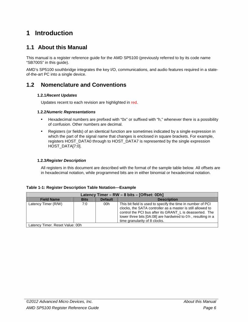
Table 1-1: Register Description Table Notation—Example
Latency Timer – RW – 8 bits – [Offset: 0Dh] Field Name Bits Default Description
Latency Timer (R/W) 7:0 00h This bit field is used to specify the time in number of PCI clocks, the SATA controller as a master is still allowed to control the PCI bus after its GRANT_L is deasserted. The lower three bits [0A:08] are hardwired to 0 h , resulting in a time granularity of 8 clocks.
Latency Timer. Reset Value: 00h
©2012 Advanced Micro Devices, Inc. Nomenclature and Conventions AMD SP5100 Register Reference Guide Page 7
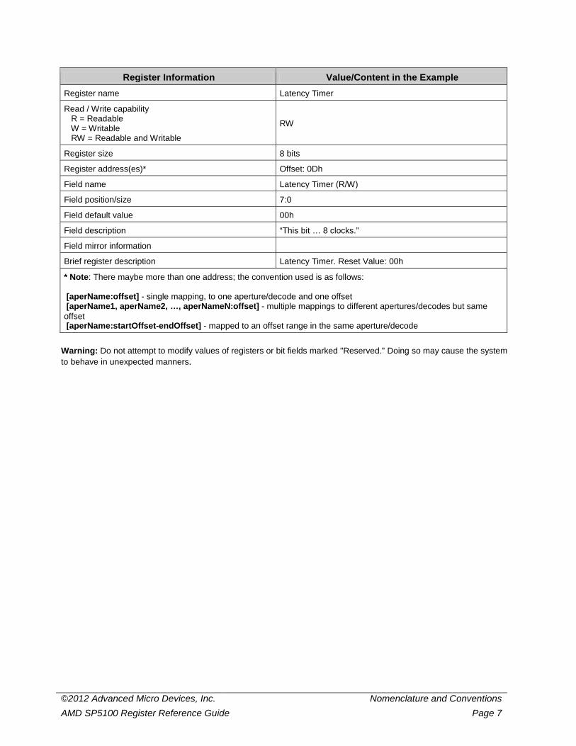
Register Information Value/Content in the Example Register name Latency Timer
Read / Write capability R = Readable W = Writable RW = Readable and Writable
RW
Register size 8 bits
Register address(es)* Offset: 0Dh
Field name Latency Timer (R/W)
Field position/size 7:0
Field default value 00h
Field description “This bit … 8 clocks.”
Field mirror information
Brief register description Latency Timer. Reset Value: 00h
* Note: There maybe more than one address; the convention used is as follows: [aperName:offset] - single mapping, to one aperture/decode and one offset [aperName1, aperName2, …, aperNameN:offset] - multiple mappings to different apertures/decodes but same offset [aperName:startOffset-endOffset] - mapped to an offset range in the same aperture/decode
Warning: Do not attempt to modify values of registers or bit fields marked "Reserved." Doing so may cause the system to behave in unexpected manners.
©2012 Advanced Micro Devices, Inc. Block Diagram AMD SP5100 Register Reference Guide Page 8
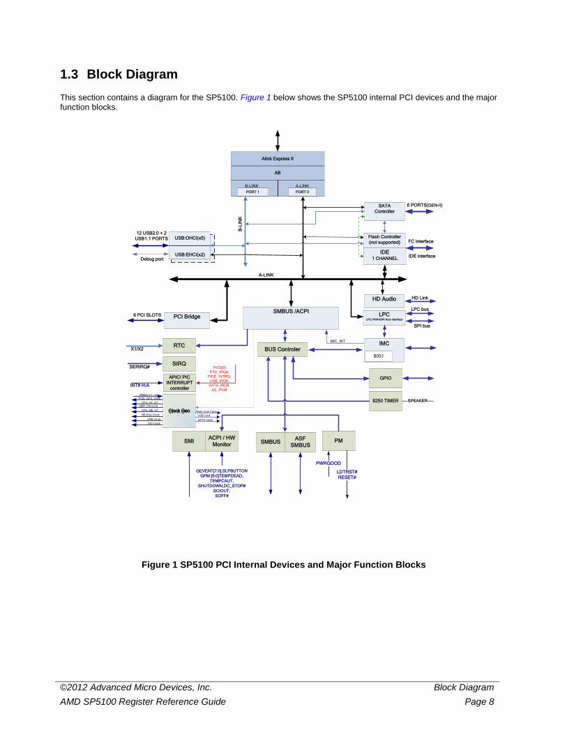
1.3 Block Diagram This section contains a diagram for the SP5100. Figure 1 below shows the SP5100 internal PCI devices and the major function blocks.
GPP_P/N (3:0)
LPCLPC /FWH/SPI Rom interface
PCI BridgeSMBUS /ACPI
AB
HD Audio
PORT 1 PORT 0
USB:OHCI(x5)
USB:EHCI(x2)
8250 TIMER
GPIO
RTC
ACPI / HW Monitor SMBUS
BUS Controler
APIC/ PICINTERRUPT
controller
SMI
SIRQ
PM
SPEAKER
GEVENT[7:0],SLPBUTTONGPM [9:0]TEMPDEAD,
TEMPCAUT,SHUTDOWN,DC_STOP#
SCIOUT, SOFF#
INT# H:A
LDTRST#RESET#
PWRGOOD
A-LINK
B-L
INK
PICD[0]RTC_IRQ#,
PIDE_INTRQ,USB_IRQ#,
SATA_IRQ#,AZ_IRQ#
X1/X2
12 USB2.0 + 2 USB1.1 PORTS
SERIRQ#
6 PCI SLOTSLPC bus
SPI bus
Debug port
B-LINK A-LINK
Alink Express II
IMC
8051
IMC_INT
Clock GenCPU_NB_HT
NB Disp Clock
USB Clock
SIO ClockSATA Clock
USB clock
Flash Cont Clock
CPU_HT_HT
PCIE_GFX_Clock25MHz X1 / X2
Flash Controller (not supported)
SATAController
6 PORTS(GEN-II)
IDE1 CHANNEL
FC interface
IDE interface
HD Link
ASF SMBUS
Figure 1 SP5100 PCI Internal Devices and Major Function Blocks
©2012 Advanced Micro Devices, Inc. Block Diagram AMD SP5100 Register Reference Guide Page 9
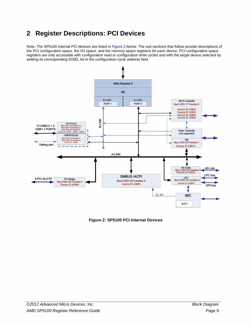
2 Register Descriptions: PCI Devices
Note: The SP5100 internal PCI devices are listed in Figure 2 below. The sub-sections that follow provide descriptions of the PCI configuration space, the I/O space, and the memory space registers for each device. PCI configuration space registers are only accessible with configuration read or configuration write cycles and with the target device selected by settling its corresponding IDSEL bit in the configuration cycle address field.
LPCPCI Bridge
Bus 0 DEV 20 Function 4Device ID 4384h
SMBUS /ACPIBus 0 DEV 20 Function 0
AB
HD Audio
PORT 1 PORT 0
USB:OHCI(x5)Bus 0 Dev 18 Function 0,1Bus 0 Dev 19 Function 0,1Bus 0 Dev 20 Function 5
Device ID 4397h : 4398h : 4399h
USB:EHCI(x2)
A-LINK
B-L
INK
12 USB2.0 + 2 USB1.1 PORTS
6 PCI SLOTSLPC bus
SPI bus
Debug port
B-LINK A-LINK
Alink Express II
IMC
8051
EC_INT
Flash Controller(not supported)
SATA Controller
IDE
HD Link
Bus 0 DEV 20 Function 1
Bus 0 DEV 20 Function 2
Bus 0 DEV 17 Function 0
Device ID 4380h
Device ID 438Ch
Device ID 438DhBus 0 DEV 20 Function 3
Device ID 4383h
Device ID 4385h
Device ID 4380hDevice ID 4380hDevice ID 4380h
Bus 0 Dev 18 Function 2Bus 0 Dev 19 Function 2
Device ID 4396h
Figure 2: SP5100 PCI Internal Devices
©2012 Advanced Micro Devices, Inc. SATA Registers (Bus 0, Device 17, Function 0) AMD SP5100 Register Reference Guide Page 10
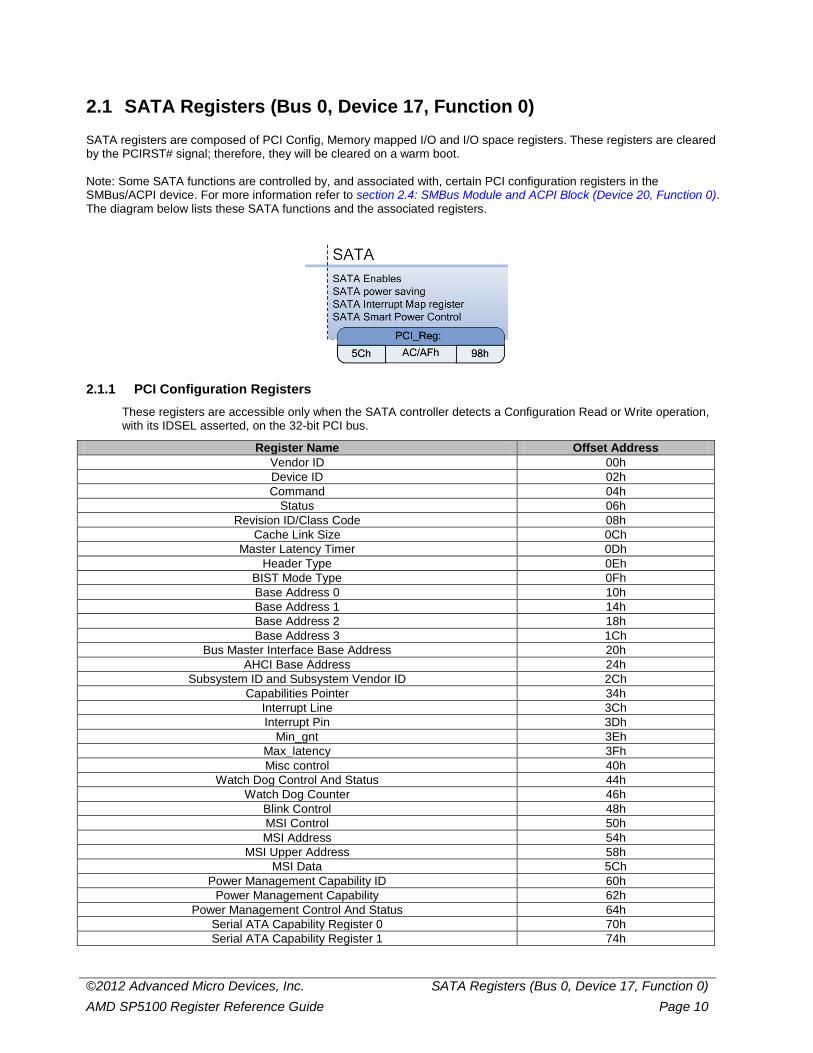
2.1 SATA Registers (Bus 0, Device 17, Function 0) SATA registers are composed of PCI Config, Memory mapped I/O and I/O space registers. These registers are cleared by the PCIRST# signal; therefore, they will be cleared on a warm boot. Note: Some SATA functions are controlled by, and associated with, certain PCI configuration registers in the SMBus/ACPI device. For more information refer to section 2.4: SMBus Module and ACPI Block (Device 20, Function 0). The diagram below lists these SATA functions and the associated registers.
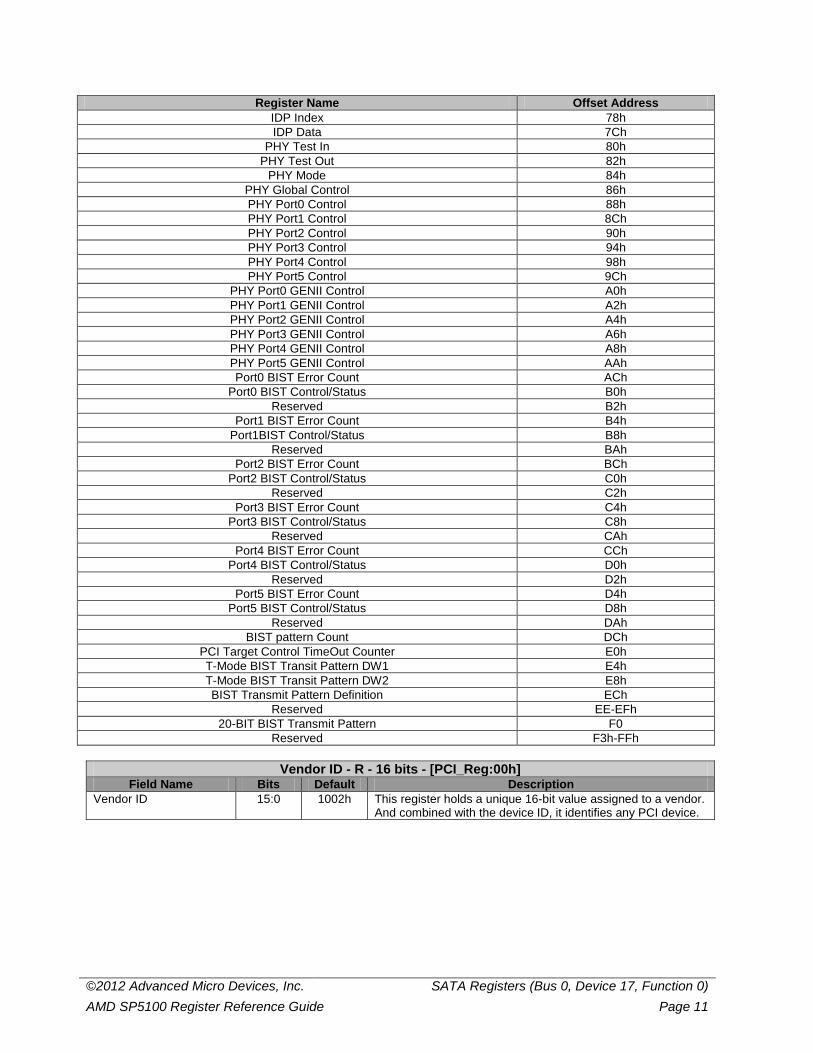
2.1.1 PCI Configuration Registers These registers are accessible only when the SATA controller detects a Configuration Read or Write operation, with its IDSEL asserted, on the 32-bit PCI bus.
Register Name Offset Address Vendor ID 00h Device ID 02h Command 04h
Status 06h Revision ID/Class Code 08h
Cache Link Size 0Ch Master Latency Timer 0Dh
Header Type 0Eh BIST Mode Type 0Fh Base Address 0 10h Base Address 1 14h Base Address 2 18h Base Address 3 1Ch
Bus Master Interface Base Address 20h AHCI Base Address 24h
Subsystem ID and Subsystem Vendor ID 2Ch Capabilities Pointer 34h
Interrupt Line 3Ch Interrupt Pin 3Dh
Min_gnt 3Eh Max_latency 3Fh Misc control 40h
Watch Dog Control And Status 44h Watch Dog Counter 46h
Blink Control 48h MSI Control 50h MSI Address 54h
MSI Upper Address 58h MSI Data 5Ch
Power Management Capability ID 60h Power Management Capability 62h
Power Management Control And Status 64h Serial ATA Capability Register 0 70h Serial ATA Capability Register 1 74h
©2012 Advanced Micro Devices, Inc. SATA Registers (Bus 0, Device 17, Function 0) AMD SP5100 Register Reference Guide Page 11
Register Name Offset Address IDP Index 78h IDP Data 7Ch
PHY Test In 80h PHY Test Out 82h
PHY Mode 84h PHY Global Control 86h PHY Port0 Control 88h PHY Port1 Control 8Ch PHY Port2 Control 90h PHY Port3 Control 94h PHY Port4 Control 98h PHY Port5 Control 9Ch
PHY Port0 GENII Control A0h PHY Port1 GENII Control A2h PHY Port2 GENII Control A4h PHY Port3 GENII Control A6h PHY Port4 GENII Control A8h PHY Port5 GENII Control AAh Port0 BIST Error Count ACh
Port0 BIST Control/Status B0h Reserved B2h
Port1 BIST Error Count B4h Port1BIST Control/Status B8h
Reserved BAh Port2 BIST Error Count BCh
Port2 BIST Control/Status C0h Reserved C2h
Port3 BIST Error Count C4h Port3 BIST Control/Status C8h
Reserved CAh Port4 BIST Error Count CCh
Port4 BIST Control/Status D0h Reserved D2h
Port5 BIST Error Count D4h Port5 BIST Control/Status D8h
Reserved DAh BIST pattern Count DCh
PCI Target Control TimeOut Counter E0h T-Mode BIST Transit Pattern DW1 E4h T-Mode BIST Transit Pattern DW2 E8h BIST Transmit Pattern Definition ECh
Reserved EE-EFh 20-BIT BIST Transmit Pattern F0
Reserved F3h-FFh
Vendor ID - R - 16 bits - [PCI_Reg:00h] Field Name Bits Default Description
Vendor ID 15:0 1002h This register holds a unique 16-bit value assigned to a vendor. And combined with the device ID, it identifies any PCI device.
©2012 Advanced Micro Devices, Inc. SATA Registers (Bus 0, Device 17, Function 0) AMD SP5100 Register Reference Guide Page 12
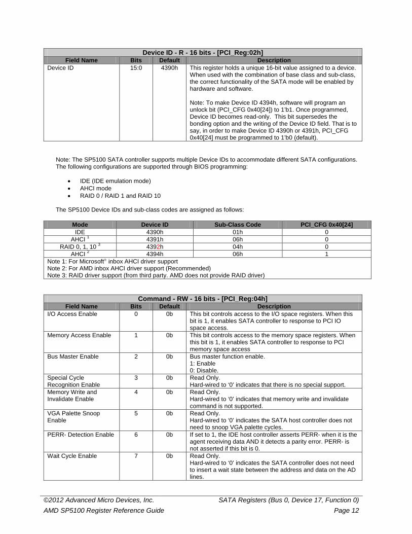
Device ID - R - 16 bits - [PCI_Reg:02h] Field Name Bits Default Description
Device ID 15:0 4390h This register holds a unique 16-bit value assigned to a device. When used with the combination of base class and sub-class, the correct functionality of the SATA mode will be enabled by hardware and software. Note: To make Device ID 4394h, software will program an unlock bit (PCI_CFG 0x40[24]) to 1’b1. Once programmed, Device ID becomes read-only. This bit supersedes the bonding option and the writing of the Device ID field. That is to say, in order to make Device ID 4390h or 4391h, PCI_CFG 0x40[24] must be programmed to 1’b0 (default).
Note: The SP5100 SATA controller supports multiple Device IDs to accommodate different SATA configurations. The following configurations are supported through BIOS programming:
• IDE (IDE emulation mode) • AHCI mode • RAID 0 / RAID 1 and RAID 10
The SP5100 Device IDs and sub-class codes are assigned as follows:
Mode Device ID Sub-Class Code PCI_CFG 0x40[24] IDE 4390h 01h 0
AHCI 1 4391h 06h 0 RAID 0, 1, 10 3 4392h 04h 0
AHCI 2 4394h 06h 1 Note 1: For Microsoft inbox AHCI driver support Note 2: For AMD inbox AHCI driver support (Recommended) Note 3: RAID driver support (from third party. AMD does not provide RAID driver)
Command - RW - 16 bits - [PCI_Reg:04h] Field Name Bits Default Description
I/O Access Enable 0 0b This bit controls access to the I/O space registers. When this bit is 1, it enables SATA controller to response to PCI IO space access.
Memory Access Enable 1 0b This bit controls access to the memory space registers. When this bit is 1, it enables SATA controller to response to PCI memory space access
Bus Master Enable 2 0b Bus master function enable. 1: Enable 0: Disable.
Special Cycle Recognition Enable
3 0b Read Only. Hard-wired to ‘0’ indicates that there is no special support.
Memory Write and Invalidate Enable
4 0b Read Only. Hard-wired to ‘0’ indicates that memory write and invalidate command is not supported.
VGA Palette Snoop Enable
5 0b Read Only. Hard-wired to ‘0’ indicates the SATA host controller does not need to snoop VGA palette cycles.
PERR- Detection Enable 6 0b If set to 1, the IDE host controller asserts PERR- when it is the agent receiving data AND it detects a parity error. PERR- is not asserted if this bit is 0.
Wait Cycle Enable 7 0b Read Only. Hard-wired to ‘0’ indicates the SATA controller does not need to insert a wait state between the address and data on the AD lines.
©2012 Advanced Micro Devices, Inc. SATA Registers (Bus 0, Device 17, Function 0) AMD SP5100 Register Reference Guide Page 13
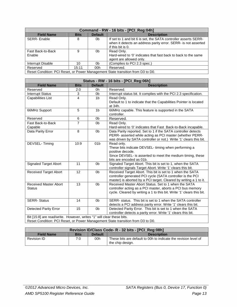
Command - RW - 16 bits - [PCI_Reg:04h] Field Name Bits Default Description
SERR- Enable 8 0b If set to 1 and bit 6 is set, the SATA controller asserts SERR- when it detects an address parity error. SERR- is not asserted if this bit is 0.
Fast Back-to-Back Enable
9 0b Read Only. Hard-wired to ‘0’ indicates that fast back to back to the same agent are allowed only.
Interrupt Disable 10 0b (Complies to PCI 2.3 spec.) Reserved 15:11 00h Reserved. Reset Condition: PCI Reset, or Power Management State transition from D3 to D0.
Status - RW - 16 bits - [PCI_Reg:06h]
Field Name Bits Default Description Reserved 2:0 0h Reserved. Interrupt Status 3 0b Interrupt status bit. It complies with the PCI 2.3 specification. Capabilities List 4 1b Read Only.
Default to 1 to indicate that the Capabilities Pointer is located at 34h.
66MHz Support 5 1b 66MHz capable. This feature is supported in the SATA controller.
Reserved 6 0b Reserved. Fast Back-to-Back Capable
7 0b Read Only. Hard-wired to ‘0’ indicates that Fast Back-to-Back incapable.
Data Parity Error 8 0b Data Parity reported. Set to 1 if the SATA controller detects PERR- asserted while acting as PCI master (whether PERR- was driven by SATA controller or not.) Write ‘1’ clears this bit.
DEVSEL- Timing 10:9 01b Read only. These bits indicate DEVSEL- timing when performing a positive decode. Since DEVSEL- is asserted to meet the medium timing, these bits are encoded as 01b.
Signaled Target Abort 11 0b Signaled Target Abort. This bit is set to 1, when the SATA controller signals Target Abort. Write ‘1’ clears this bit.
Received Target Abort 12 0b Received Target Abort. This bit is set to 1 when the SATA controller generated PCI cycle (SATA controller is the PCI master) is aborted by a PCI target. Cleared by writing a 1 to it.
Received Master Abort Status
13 0b Received Master Abort Status. Set to 1 when the SATA controller acting as a PCI master, aborts a PCI bus memory cycle. Cleared by writing a 1 to this bit. Write ‘1’ clears this bit.
SERR- Status 14 0b SERR- status. This bit is set to 1 when the SATA controller detects a PCI address parity error. Write ‘1’ clears this bit.
Detected Parity Error 15 0b Detected Parity Error. This bit is set to 1 when the SATA controller detects a parity error. Write ‘1’ clears this bit.
Bit [15:8] are read/write. However, writes “1” will clear these bits. Reset Condition: PCI Reset, or Power Management State transition from D3 to D0.
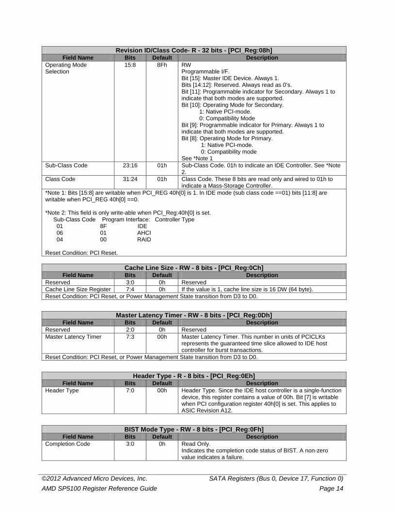
Revision ID/Class Code- R - 32 bits - [PCI_Reg:08h]
Field Name Bits Default Description Revision ID 7:0 00h These bits are default to 00h to indicate the revision level of
the chip design.
©2012 Advanced Micro Devices, Inc. SATA Registers (Bus 0, Device 17, Function 0) AMD SP5100 Register Reference Guide Page 14
Revision ID/Class Code- R - 32 bits - [PCI_Reg:08h] Field Name Bits Default Description
Operating Mode Selection
15:8 8Fh RW Programmable I/F. Bit [15]: Master IDE Device. Always 1. Bits [14:12]: Reserved. Always read as 0’s. Bit [11]: Programmable indicator for Secondary. Always 1 to indicate that both modes are supported. Bit [10]: Operating Mode for Secondary. 1: Native PCI-mode. 0: Compatibility Mode Bit [9]: Programmable indicator for Primary. Always 1 to indicate that both modes are supported. Bit [8]: Operating Mode for Primary. 1: Native PCI-mode. 0: Compatibility mode See *Note 1
Sub-Class Code 23:16 01h Sub-Class Code. 01h to indicate an IDE Controller. See *Note 2.
Class Code 31:24 01h Class Code. These 8 bits are read only and wired to 01h to indicate a Mass-Storage Controller.
*Note 1: Bits [15:8] are writable when PCI_REG 40h[0] is 1. In IDE mode (sub class code ==01) bits [11:8] are writable when PCI_REG 40h[0] ==0. *Note 2: This field is only write-able when PCI_Reg:40h[0] is set. Sub-Class Code Program Interface: Controller Type 01 8F IDE 06 01 AHCI 04 00 RAID Reset Condition: PCI Reset.
Cache Line Size - RW - 8 bits - [PCI_Reg:0Ch]
Field Name Bits Default Description Reserved 3:0 0h Reserved Cache Line Size Register 7:4 0h If the value is 1, cache line size is 16 DW (64 byte). Reset Condition: PCI Reset, or Power Management State transition from D3 to D0.
Master Latency Timer - RW - 8 bits - [PCI_Reg:0Dh] Field Name Bits Default Description
Reserved 2:0 0h Reserved Master Latency Timer 7:3 00h Master Latency Timer. This number in units of PCICLKs
represents the guaranteed time slice allowed to IDE host controller for burst transactions.
Reset Condition: PCI Reset, or Power Management State transition from D3 to D0.
Header Type - R - 8 bits - [PCI_Reg:0Eh] Field Name Bits Default Description
Header Type 7:0 00h Header Type. Since the IDE host controller is a single-function device, this register contains a value of 00h. Bit [7] is writable when PCI configuration register 40h[0] is set. This applies to ASIC Revision A12.
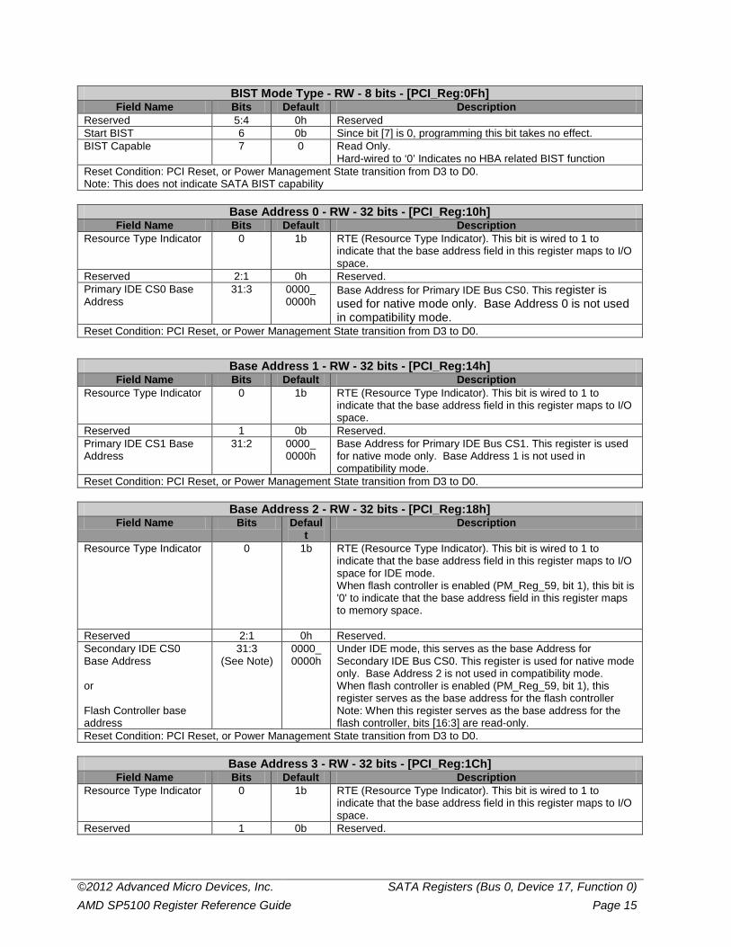
BIST Mode Type - RW - 8 bits - [PCI_Reg:0Fh] Field Name Bits Default Description
Completion Code 3:0 0h Read Only. Indicates the completion code status of BIST. A non-zero value indicates a failure.
©2012 Advanced Micro Devices, Inc. SATA Registers (Bus 0, Device 17, Function 0) AMD SP5100 Register Reference Guide Page 15
BIST Mode Type - RW - 8 bits - [PCI_Reg:0Fh] Field Name Bits Default Description
Reserved 5:4 0h Reserved Start BIST 6 0b Since bit [7] is 0, programming this bit takes no effect. BIST Capable 7 0 Read Only.
Hard-wired to ‘0’ Indicates no HBA related BIST function Reset Condition: PCI Reset, or Power Management State transition from D3 to D0. Note: This does not indicate SATA BIST capability
Base Address 0 - RW - 32 bits - [PCI_Reg:10h]
Field Name Bits Default Description Resource Type Indicator
0 1b RTE (Resource Type Indicator). This bit is wired to 1 to indicate that the base address field in this register maps to I/O space.
Reserved 2:1 0h Reserved. Primary IDE CS0 Base Address
31:3 0000_ 0000h
Base Address for Primary IDE Bus CS0. This register is used for native mode only. Base Address 0 is not used in compatibility mode.
Reset Condition: PCI Reset, or Power Management State transition from D3 to D0.
Base Address 1 - RW - 32 bits - [PCI_Reg:14h] Field Name Bits Default Description
Resource Type Indicator
0 1b RTE (Resource Type Indicator). This bit is wired to 1 to indicate that the base address field in this register maps to I/O space.
Reserved 1 0b Reserved. Primary IDE CS1 Base Address
31:2 0000_ 0000h
Base Address for Primary IDE Bus CS1. This register is used for native mode only. Base Address 1 is not used in compatibility mode.
Reset Condition: PCI Reset, or Power Management State transition from D3 to D0.
Base Address 2 - RW - 32 bits - [PCI_Reg:18h] Field Name Bits Defaul
t Description
Resource Type Indicator 0 1b RTE (Resource Type Indicator). This bit is wired to 1 to indicate that the base address field in this register maps to I/O space for IDE mode. When flash controller is enabled (PM_Reg_59, bit 1), this bit is '0' to indicate that the base address field in this register maps to memory space.
Reserved 2:1 0h Reserved. Secondary IDE CS0 Base Address or Flash Controller base address
31:3 (See Note)
0000_ 0000h
Under IDE mode, this serves as the base Address for Secondary IDE Bus CS0. This register is used for native mode only. Base Address 2 is not used in compatibility mode. When flash controller is enabled (PM_Reg_59, bit 1), this register serves as the base address for the flash controller Note: When this register serves as the base address for the flash controller, bits [16:3] are read-only.
Reset Condition: PCI Reset, or Power Management State transition from D3 to D0.
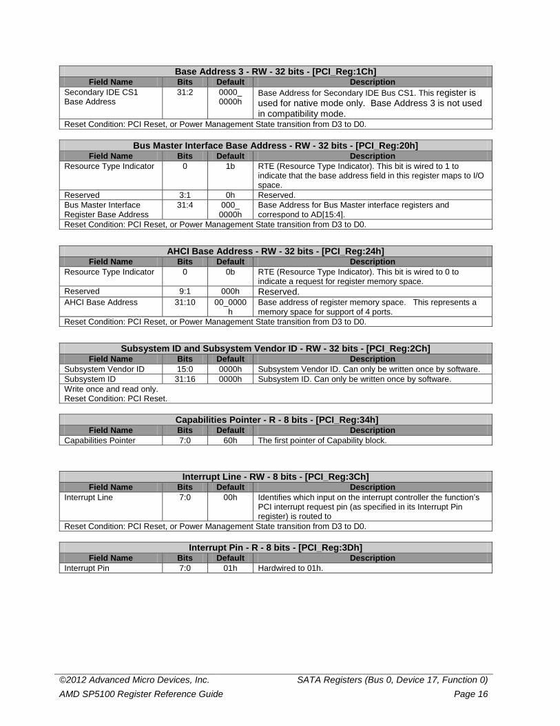
Base Address 3 - RW - 32 bits - [PCI_Reg:1Ch] Field Name Bits Default Description
Resource Type Indicator 0 1b RTE (Resource Type Indicator). This bit is wired to 1 to indicate that the base address field in this register maps to I/O space.
Reserved 1 0b Reserved.
©2012 Advanced Micro Devices, Inc. SATA Registers (Bus 0, Device 17, Function 0) AMD SP5100 Register Reference Guide Page 16
Base Address 3 - RW - 32 bits - [PCI_Reg:1Ch] Field Name Bits Default Description
Secondary IDE CS1 Base Address
31:2 0000_ 0000h
Base Address for Secondary IDE Bus CS1. This register is used for native mode only. Base Address 3 is not used in compatibility mode.
Reset Condition: PCI Reset, or Power Management State transition from D3 to D0.
Bus Master Interface Base Address - RW - 32 bits - [PCI_Reg:20h] Field Name Bits Default Description
Resource Type Indicator 0 1b RTE (Resource Type Indicator). This bit is wired to 1 to indicate that the base address field in this register maps to I/O space.
Reserved 3:1 0h Reserved. Bus Master Interface Register Base Address
31:4 000_ 0000h
Base Address for Bus Master interface registers and correspond to AD[15:4].
Reset Condition: PCI Reset, or Power Management State transition from D3 to D0.
AHCI Base Address - RW - 32 bits - [PCI_Reg:24h] Field Name Bits Default Description
Resource Type Indicator
0 0b RTE (Resource Type Indicator). This bit is wired to 0 to indicate a request for register memory space.
Reserved 9:1 000h Reserved. AHCI Base Address 31:10 00_0000
h Base address of register memory space. This represents a memory space for support of 4 ports.
Reset Condition: PCI Reset, or Power Management State transition from D3 to D0.
Subsystem ID and Subsystem Vendor ID - RW - 32 bits - [PCI_Reg:2Ch] Field Name Bits Default Description
Subsystem Vendor ID 15:0 0000h Subsystem Vendor ID. Can only be written once by software. Subsystem ID 31:16 0000h Subsystem ID. Can only be written once by software. Write once and read only. Reset Condition: PCI Reset.
Capabilities Pointer - R - 8 bits - [PCI_Reg:34h]
Field Name Bits Default Description Capabilities Pointer 7:0 60h The first pointer of Capability block.
Interrupt Line - RW - 8 bits - [PCI_Reg:3Ch] Field Name Bits Default Description
Interrupt Line 7:0 00h Identifies which input on the interrupt controller the function’s PCI interrupt request pin (as specified in its Interrupt Pin register) is routed to
Reset Condition: PCI Reset, or Power Management State transition from D3 to D0.
Interrupt Pin - R - 8 bits - [PCI_Reg:3Dh] Field Name Bits Default Description
Interrupt Pin 7:0 01h Hardwired to 01h.
©2012 Advanced Micro Devices, Inc. SATA Registers (Bus 0, Device 17, Function 0) AMD SP5100 Register Reference Guide Page 17
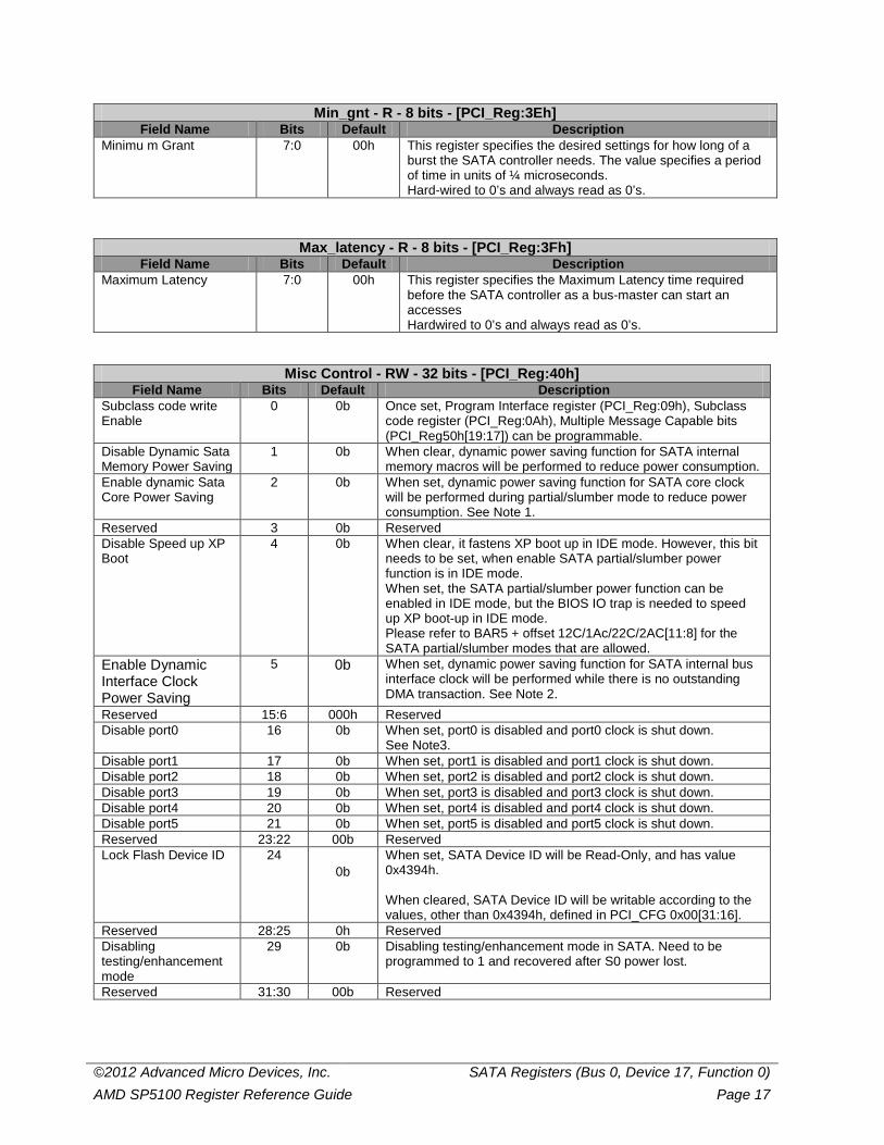
Min_gnt - R - 8 bits - [PCI_Reg:3Eh] Field Name Bits Default Description
Minimu m Grant 7:0 00h This register specifies the desired settings for how long of a burst the SATA controller needs. The value specifies a period of time in units of ¼ microseconds. Hard-wired to 0’s and always read as 0’s.
Max_latency - R - 8 bits - [PCI_Reg:3Fh] Field Name Bits Default Description
Maximum Latency
7:0 00h This register specifies the Maximum Latency time required before the SATA controller as a bus-master can start an accesses Hardwired to 0’s and always read as 0’s.
Misc Control - RW - 32 bits - [PCI_Reg:40h] Field Name Bits Default Description
Subclass code write Enable
0 0b Once set, Program Interface register (PCI_Reg:09h), Subclass code register (PCI_Reg:0Ah), Multiple Message Capable bits (PCI_Reg50h[19:17]) can be programmable.
Disable Dynamic Sata Memory Power Saving
1 0b When clear, dynamic power saving function for SATA internal memory macros will be performed to reduce power consumption.
Enable dynamic Sata Core Power Saving
2 0b When set, dynamic power saving function for SATA core clock will be performed during partial/slumber mode to reduce power consumption. See Note 1.
Reserved 3 0b Reserved Disable Speed up XP Boot
4 0b When clear, it fastens XP boot up in IDE mode. However, this bit needs to be set, when enable SATA partial/slumber power function is in IDE mode. When set, the SATA partial/slumber power function can be enabled in IDE mode, but the BIOS IO trap is needed to speed up XP boot-up in IDE mode. Please refer to BAR5 + offset 12C/1Ac/22C/2AC[11:8] for the SATA partial/slumber modes that are allowed.
Enable Dynamic Interface Clock Power Saving
5 0b When set, dynamic power saving function for SATA internal bus interface clock will be performed while there is no outstanding DMA transaction. See Note 2.
Reserved 15:6 000h Reserved Disable port0 16 0b When set, port0 is disabled and port0 clock is shut down.
See Note3. Disable port1 17 0b When set, port1 is disabled and port1 clock is shut down. Disable port2 18 0b When set, port2 is disabled and port2 clock is shut down. Disable port3 19 0b When set, port3 is disabled and port3 clock is shut down. Disable port4 20 0b When set, port4 is disabled and port4 clock is shut down. Disable port5 21 0b When set, port5 is disabled and port5 clock is shut down. Reserved 23:22 00b Reserved Lock Flash Device ID 24
0b When set, SATA Device ID will be Read-Only, and has value 0x4394h. When cleared, SATA Device ID will be writable according to the values, other than 0x4394h, defined in PCI_CFG 0x00[31:16].
Reserved 28:25 0h Reserved Disabling testing/enhancement mode
29 0b Disabling testing/enhancement mode in SATA. Need to be programmed to 1 and recovered after S0 power lost.
Reserved 31:30 00b Reserved
©2012 Advanced Micro Devices, Inc. SATA Registers (Bus 0, Device 17, Function 0) AMD SP5100 Register Reference Guide Page 18
Misc Control - RW - 32 bits - [PCI_Reg:40h] Field Name Bits Default Description
Reset Condition: PCI Reset. Note1: Bit [2]: To enable dynamic sataclk shut down function. Sataclk will be shut down during partial/slumber mode. It will automatically wake-up when received new commands from software, or received COMWAKE/COMINIT from device. This function will be effective when this bit is set also ACPI-PCI_reg ACh[13] Note2: When set, enable dynamic blink clock shut down. Blink clk will be shut down when there is no outstanding DMA operation. “BAR4 + offset 0/8h[0] = 1’b1”,or “BAR5 +offset 134/1B4/234/2B4[31:0] = non-zeros” ,or “BAR5 +offset 138/1B8/238/2B8[31:0] = non-zeros” means there is DMA operation on going. Note3: When set, put PHY port0 is disabled, shut down port0 clock at link/transport layer.
Watch Dog Control And Status - RW - 16 bits - [PCI_Reg:44h]
Field Name Bits Default Description Watchdog Enable 0 0b Set the bit to enable the watchdog counter for all the PCI down
stream transaction for both SATA and PATA ports. Watchdog Timeout Status
1 0b Watchdog Counter Timeout Status bit. This bit indicates that the watchdog counter has expired for PCI down stream transaction and the transaction got aborted due to the fact that the counter has expired. Software writes 1 to clear the status
PATA Watchdog Timeout Status
2 0b PATA Watchdog Counter Timeout Status bit. This bit indicates that the watchdog counter in a PATA port has expired for PCI down stream transaction and the transaction got aborted due to counter has expired. Software writes 1 to clear the status
Reserved 15:3 0000h Reserved. Still read/write-able. This register is used from preventing system hang. Reset Condition: PCI Reset, or Power Management State transition from D3 to D0.
Watch Dog Counter - RW - 16 bits - [PCI_Reg:46h]
Field Name Bits Default Description Watchdog Counter 7:0 80h Specifies the timeout retry count for PCI down stream retries.
This value is used for both SATA and PATA ports. Reserved 15:8 00h Reserved. Still read/write-able. This register is used from preventing system hang. Reset Condition: PCI Reset, or Power Management State transition from D3 to D0.
B-Link Control - RW - 32 bits - [PCI_Reg:48h]
Field Name Bits Default Description Reserved 23:0 00_
0000h Reserved. Still read/write-able.
Disabling testing/enhancement mode
24 0b Disabling testing/enhancement mode in SATA. Need to be programmed to 1 and recovered after S0 power lost.
Reserved 31:25 00h Reserved. Still read/write-able. Reset Condition: PCI Reset, or Power Management State transition from D3 to D0.
MSI Control - RW- 32 bits - [PCI_Reg:50h]
Field Name Bits Default Description Capability ID 7:0 05h Read-Only.
Capability ID. Indicates this is MSI capability ID. Capability Next Pointer 15:8 70h Read-Only.
Next Pointer (Default to 70h, points to Index Data pair capability).
Message Signaled Interrupt Enable
16 0b MSI Enable
©2012 Advanced Micro Devices, Inc. SATA Registers (Bus 0, Device 17, Function 0) AMD SP5100 Register Reference Guide Page 19
MSI Control - RW- 32 bits - [PCI_Reg:50h] Field Name Bits Default Description
Multiple Message Capable
19:17 010b Multiple Message Capable (MMC). *Note
Multiple Message Enable 22:20 0h Multiple Message Enable (MME). MSI 64-bit Address 23 1b Read Only
64-bit address supported Reserved 31:24 00h Reserved. Reset Condition: PCI Reset, or Power Management State transition from D3 to D0.
MSI Address - RW- 32 bits - [PCI_Reg:54h] Field Name Bits Default Description
Reserved 1:0 0h Reserved. MSI Address 31:2 0000_0000h Lower 32 bits of the system specified message address
always DW aligned. Reset Condition: PCI Reset, or Power Management State transition from D3 to D0.
MSI Upper Address - RW- 32 bits - [PCI_Reg:58h] Field Name Bits Default Description
MSI Upper Address 31:0 0000_0000h MSI Upper Address: Upper 32 bits of the system specified message address. This register is optional and only implemented if MC.C64=1.
Reset Condition: PCI Reset, or Power Management State transition from D3 to D0.
MSI Data - RW- 16 bits - [PCI_Reg:5Ch] Field Name Bits Default Description
MSI Data 15:0 0000h MSI Data Reset Condition: PCI Reset, or Power Management State transition from D3 to D0.
Power Management Capability ID – R - 16 bits - [PCI_Reg:60h]
Field Name Bits Default Description Capability ID 7:0 01h Capability ID (Default to 01h, indicates that this pointer is a
PCI power management). Capability Next Pointer 15:8 50h Next Pointer (hard wired to 50h, points to MSI capability. Reset Condition: PCI Reset, or Power Management State transition from D3 to D0.
Power Management Capability - R- 16 bits - [PCI_Reg:62h]
Field Name Bits Default Description Version (VS) 2:0 010b Indicates support for Revision 1.1 of the PCI Power
Management Specification. PME Clock (PMEC) 3 0b Indicates that PCI clock is not required to generate PME#. Reserved 4 0b Reserved Device Specific Initialization
5 1b Indicates whether device-specific initialization is required. Hard wire to 1.
Aux_Current 8:6 0h Reports the maximum Suspend well current required when in the D3COLD state. Hard wire to 000b.
D1_Support 9 0b The D1 state is not supported. D2_Support 10 0b The D2 state is not supported. PME_Support 15:11 00h Hard wired to 00h.
©2012 Advanced Micro Devices, Inc. SATA Registers (Bus 0, Device 17, Function 0) AMD SP5100 Register Reference Guide Page 20
PCI Power Management Control And Status - RW- 16 bits - [PCI_Reg:64h] Field Name Bits Default Description
Power State (PS) 1:0 00b This field is used both to determine the current power state of the HBA and to set a new power state. The values are:
00 – D0 state 11 – D3HOT state
The D1 and D2 states are not supported. When in the D3HOT state, the configuration space is available, but the register memory spaces are not. Additionally, interrupts are blocked.
Reserved 7:2 00h Reserved PME Enable (PMEE) 8 0b Read Only.
Hard-wired to ‘0’ indicates PME disable Reserved 14:9 00h Reserved. PME Status 15 0b Read Only.
Hard-wired to ‘0’ as PME disable Reset Condition: PCI Reset.
Serial ATA Capability Register 0 - R- 32 bits - [PCI_Reg:70h]
Field Name Bits Default Description Capability ID 7:0 12h Capability ID (hard wired to 12h, indicates that this pointer is a
Serial ATA Capability) Capability Next Pointer 15:8 00h Next Pointer. end of list. Minor Revision 19:16 0h Minor revision number of the SATA Capability Pointer
implemented. Major Revision 23:20 1h Major revision number of the SATA Capability Pointer
implemented. Reserved 31:24 00h Reserved This set of registers when supported is used for the Index-Data Pair mechanism.
Serial ATA Capability Register 1 - R- 32 bits - [PCI_Reg:74h]
Field Name Bits Default Description BAR Location 3:0 1111b Value 1111b Indicates Index-Data pair is implemented in
Dwords directly following SATACR1 in the PCI configuration space.
BAR Offset 23:4 000h Indicates the offset into the BAR where the Index-Data Pair are located in Dword granularity.
Reserved 31:24 00h Reserved. This set of registers when supported is used for the Index-Data Pair mechanism.
IDP Index Register - RW- 32 bits - [PCI_Reg:78h]
Field Name Bits Default Description Reserved 1:0 0h Reserved. IDP Index 9:2 00h This register selects the Dword offset of the memory mapped
AHCI register to be accessed. The IDP Index should be sized such that it can access the entire ABAR register space for the particular implementation.
Reserved 31:10 00_0000h
Reserved
This set of registers, when supported, is used for the Index-Data Pair mechanism. Reset Condition: PCI Reset, or Power Management State transition from D3 to D0.
©2012 Advanced Micro Devices, Inc. SATA Registers (Bus 0, Device 17, Function 0) AMD SP5100 Register Reference Guide Page 21
IDP Data Register - RW- 32 bits - [PCI_Reg:7Ch] Field Name Bits Default Description
IDP Data 31:0 F722_FF85h
This register is a “window” through which data is read or written to the memory mapped register pointed to by the IDP Index register. Note that a physical register is not actually implemented as the data is actually stored in the memory mapped registers. Since this is not a physical register, the “default” value is the same as the default value of the register pointed to by IDP Index.
All register accesses to IDP Data are Dword granularity.
PHY Test In - RW- 16 bits - [PCI_Reg:80h]
Field Name Bits Default Description PHY transmission enable 0 0b SATA PHY transmisión enable (txen) PHY transmission clock 1 0b SATA PHY transmisión clock (tbc) PHY Test Input data 11:2 000h SATA PHY transmisión data (txd0:9) Reserved 15:12 0h Reserved. Still read/write-able. Reset Condition: PCI Reset, or Power Management State transition from D3 to D0.
PHY Test Out - R- 16 bits - [PCI_Reg:82h]
Field Name Bits Default Description PHY Test Output data 9:0 000h SATA PHY receiving data (rxd9:0) PHY receiving clock 10 0b SATA PHY receiving clock (asicclk) PHY receiving data valid 11 0b SATA PHY receiving data valid (rxdvalid) PHY receiving signal valid
12 0b SATA PHY receiving signal valid (sglvalid)
Reserved 15:13 0h Reserved. Still read/write-able.
PHY MODE- RW - 16 bits - [PCI_Reg:84h]
Field Name Bits Default Description OSCDISABLE 0 0b Set to ‘1’ to disable PHY Crystal SATA PHY Enable 1 1b If set, PHY is enabled. PHY Global ResetB 2 1b Active low bit, clear the bit to reset all 4 ports logic in PHY. Port0 Reset 3 0b Set the bit to reset PHY port0 logic. Port1 Reset 4 0b Set the bit to reset PHY port1 logic. Port2 Reset 5 0b Set the bit to reset PHY port2 logic. Port3 Reset 6 0b Set the bit to reset PHY port3 logic. Port4 Reset 7 0b Set the bit to reset PHY port4 logic. Port5 Reset 8 0b Set the bit to reset PHY port5 logic. TESTMODE 9 0b Read Only
Output of PHY, indicates PHY is in test mode. Reserved 15:10 00h Reserved. Still read/write-able. Reset Condition: PCI Reset, or Power Management State transition from D3 to D0.
PHY Global Register - RW- 16 bits - [PCI_Reg:86h]
Field Name Bits Default Description PHY Global Control 15:0 2C40h PHY global fine-tune register.
Bit[6] = EXTCLKEN=1’b1, enables the 100MHz Diff Clock. Default enabled. Bit[15] has no effect, actual control in sata_core (clksel) Bit[4] has no effect, actual logia in sata_core (refmode)
Reset Condition: PCI Reset.
©2012 Advanced Micro Devices, Inc. SATA Registers (Bus 0, Device 17, Function 0) AMD SP5100 Register Reference Guide Page 22
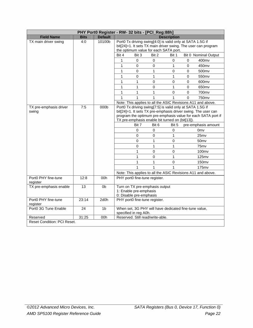
PHY Port0 Register - RW- 32 bits - [PCI_Reg:88h] Field Name Bits Default Description
TX main driver swing 4:0 10100b Port0 Tx driving swing[4:0] is valid only at SATA 1.5G if bit[24]=1. It sets TX main driver swing. The user can program the optimum value for each SATA port. Bit 4 Bit 3 Bit 2 Bit 1 Bit 0 Nominal Output 1 0 0 0 0 400mv 1 0 0 1 0 450mv 1 0 1 0 0 500mv 1 0 1 1 0 550mv 1 1 0 0 0 600mv 1 1 0 1 0 650mv 1 1 1 0 0 700mv 1 1 1 1 0 750mv Note: This applies to all the ASIC Revisions A11 and above.
TX pre-emphasis driver swing
7:5 000b Port0 Tx driving swing[7:5] is valid only at SATA 1.5G if bit[24]=1. It sets TX pre-emphasis driver swing. The user can program the optimum pre-emphasis value for each SATA port if TX pre-emphasis enable bit turned on (bit[13]). Bit 7 Bit 6 Bit 5 pre-emphasis amount 0 0 0 0mv 0 0 1 25mv 0 1 0 50mv 0 1 1 75mv 1 0 0 100mv 1 0 1 125mv 1 1 0 150mv 1 1 1 175mv Note: This applies to all the ASIC Revisions A11 and above.
Port0 PHY fine-tune register
12:8 00h PHY port0 fine-tune register.
TX pre-emphasis enable 13 0b Turn on TX pre-emphasis output 1: Enable pre-emphasis 0: Disable pre-emphasis
Port0 PHY fine-tune register
23:14 2d0h PHY port0 fine-tune register.
Port0 3G Tune Enable 24 1b When set, 3G PHY will have dedicated fine-tune value, specified in reg A0h.
Reserved 31:25 00h Reserved. Still read/write-able. Reset Condition: PCI Reset.
©2012 Advanced Micro Devices, Inc. SATA Registers (Bus 0, Device 17, Function 0) AMD SP5100 Register Reference Guide Page 23
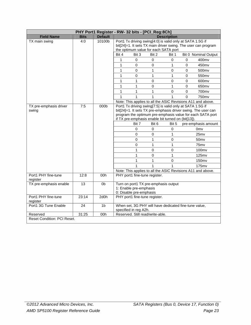
PHY Port1 Register - RW- 32 bits - [PCI_Reg:8Ch] Field Name Bits Default Description
TX main swing 4:0 10100b Port1 Tx driving swing[4:0] is valid only at SATA 1.5G if bit[24]=1. It sets TX main driver swing. The user can program the optimum value for each SATA port Bit 4 Bit 3 Bit 2 Bit 1 Bit 0 Nominal Output 1 0 0 0 0 400mv 1 0 0 1 0 450mv 1 0 1 0 0 500mv 1 0 1 1 0 550mv 1 1 0 0 0 600mv 1 1 0 1 0 650mv 1 1 1 0 0 700mv 1 1 1 1 0 750mv Note: This applies to all the ASIC Revisions A11 and above.
TX pre-emphasis driver swing
7:5 000b Port1 Tx driving swing[7:5] is valid only at SATA 1.5G if bit[24]=1. It sets TX pre-emphasis driver swing. The user can program the optimum pre-emphasis value for each SATA port if TX pre-emphasis enable bit turned on (bit[13]). Bit 7 Bit 6 Bit 5 pre-emphasis amount 0 0 0 0mv 0 0 1 25mv 0 1 0 50mv 0 1 1 75mv 1 0 0 100mv 1 0 1 125mv 1 1 0 150mv 1 1 1 175mv Note: This applies to all the ASIC Revisions A11 and above.
Port1 PHY fine-tune register
12:8 00h PHY port1 fine-tune register.
TX pre-emphasis enable 13 0b Turn on port1 TX pre-emphasis output 1: Enable pre-emphasis 0: Disable pre-emphasis
Port1 PHY fine-tune register
23:14 2d0h PHY port1 fine-tune register.
Port1 3G Tune Enable 24 1b When set, 3G PHY will have dedicated fine-tune value, specified in reg A2h.
Reserved 31:25 00h Reserved. Still read/write-able. Reset Condition: PCI Reset.

©2012 Advanced Micro Devices, Inc. SATA Registers (Bus 0, Device 17, Function 0) AMD SP5100 Register Reference Guide Page 24
PHY Port2 Register - RW- 32 bits - [PCI_Reg:90h] Field Name Bits Default Description
TX main swing 4:0 10100b Port2 Tx driving swing[4:0] is valid only at SATA 1.5G if bit[24]=1. It sets TX main driver swing. The user can program the optimum value for each SATA port. Bit 4 Bit 3 Bit 2 Bit 1 Bit 0 Nominal Output 1 0 0 0 0 400mv 1 0 0 1 0 450mv 1 0 1 0 0 500mv 1 0 1 1 0 550mv 1 1 0 1 0 600mv 1 1 0 1 0 650mv 1 1 1 0 0 700mv 1 1 1 1 0 750mv Note: This applies to all the ASIC Revisions A11 and above.
TX pre-emphasis driver swing
7:5 000b Port2 Tx driving swing[7:5] is valid only at SATA 1.5G if bit[24]=1. It sets TX pre-emphasis driver swing. The user can program the optimum pre-emphasis value for each SATA port if TX pre-emphasis enable bit turned on (bit[13]). Bit 7 Bit 6 Bit 5 pre-emphasis amount 0 0 0 0mv 0 0 1 25mv 0 1 0 50mv 0 1 1 75mv 1 0 0 100mv 1 0 1 125mv 1 1 0 150mv 1 1 1 175mv Note: This applies to all the ASIC Revisions A11 and above.
Port2 PHY fine-tune register
12:8 00h PHY port2 fine-tune register.
TX pre-emphasis enable 13 0b Turn on port2 TX pre-emphasis output 1: Enable pre-emphasis 0: Disable pre-emphasis
Port2 PHY fine-tune register
23:14 2d0h PHY port2 fine-tune register.
Port2 3G Tune Enable 24 1b When set, 3G PHY will have dedicated fine-tune value, specified in reg A4h.
Reserved 31:25 00h Reserved. Reset Condition: PCI Reset.

©2012 Advanced Micro Devices, Inc. SATA Registers (Bus 0, Device 17, Function 0) AMD SP5100 Register Reference Guide Page 25
PHY Port3 Register - RW- 32 bits - [PCI_Reg:94h] Field Name Bits Default Description
TX main swing 4:0 10100b Port3 Tx driving swing[4:0] is valid only at SATA 1.5G if bit[24]=1. It sets TX main driver swing. The user can program the optimum value for each SATA port. Bit 4 Bit 3 Bit 2 Bit 1 Bit 0 Nominal Output 1 0 0 0 0 400mv 1 0 0 1 0 450mv 1 0 1 0 0 500mv 1 0 1 1 0 550mv 1 1 0 0 0 600mv 1 1 0 1 0 650mv 1 1 1 0 0 700mv 1 1 1 1 0 750mv Note: This applies to all the ASIC Revisions A11 and above.
TX pre-emphasis driver swing
7:5 000b Port3 Tx driving swing[7:5] is valid only at SATA 1.5G if bit[24]=1. It sets TX pre-emphasis driver swing. The user can program the optimum pre-emphasis value for each SATA port if TX pre-emphasis enable bit turned on (bit[13]). Bit 7 Bit 6 Bit 5 pre-emphasis amount 0 0 0 0mv 0 0 1 25mv 0 1 0 50mv 0 1 1 75mv 1 0 0 100mv 1 0 1 125mv 1 1 0 150mv 1 1 1 175mv Note: This applies to all the ASIC Revisions A11 and above.
Port3 PHY fine-tune register
12:8 00h PHY port3 fine-tune register.
TX pre-emphasis enable 13 0b Turn on port3 TX pre-emphasis output 1: Enable pre-emphasis 0: Disable pre-emphasis
Port3 PHY fine-tune register
23:14 2d0h PHY port3 fine-tune register.
Port3 3G Tune Enable 24 1b When set, 3G PHY will have dedicated fine-tune value, specified in reg A6h.
Reserved 31:25 00h Reserved. Reset Condition: PCI Reset.
©2012 Advanced Micro Devices, Inc. SATA Registers (Bus 0, Device 17, Function 0) AMD SP5100 Register Reference Guide Page 26
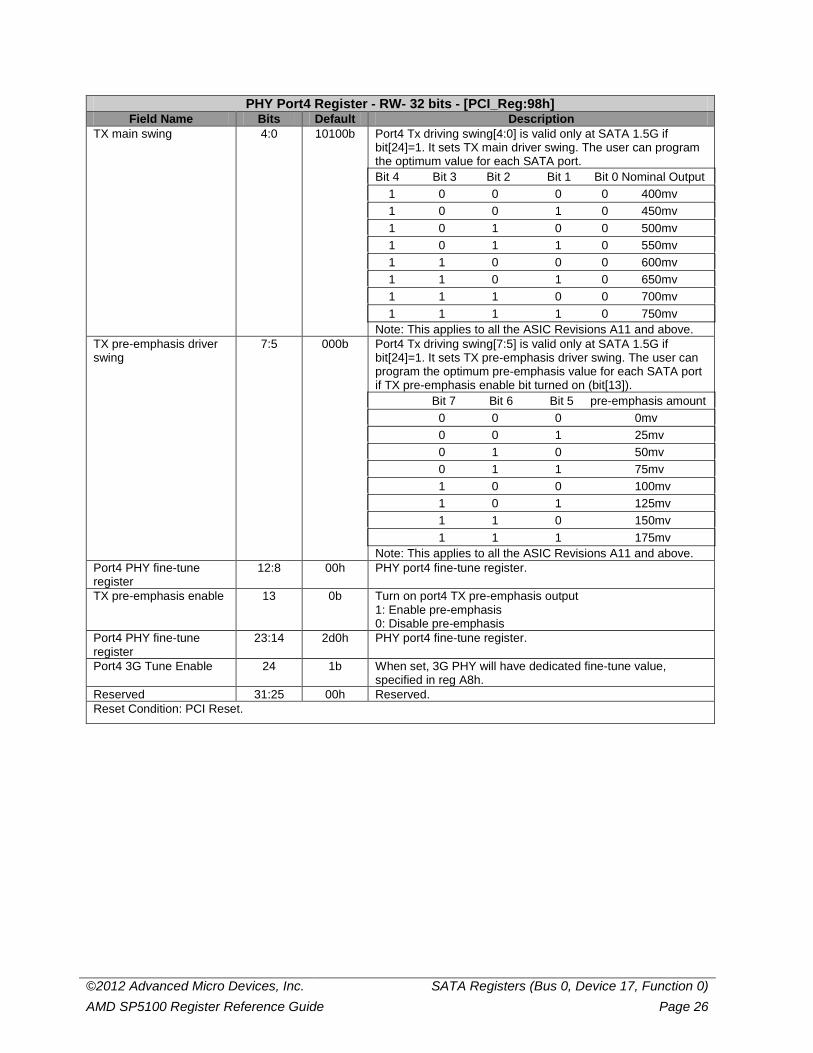
PHY Port4 Register - RW- 32 bits - [PCI_Reg:98h] Field Name Bits Default Description
TX main swing 4:0 10100b Port4 Tx driving swing[4:0] is valid only at SATA 1.5G if bit[24]=1. It sets TX main driver swing. The user can program the optimum value for each SATA port. Bit 4 Bit 3 Bit 2 Bit 1 Bit 0 Nominal Output 1 0 0 0 0 400mv 1 0 0 1 0 450mv 1 0 1 0 0 500mv 1 0 1 1 0 550mv 1 1 0 0 0 600mv 1 1 0 1 0 650mv 1 1 1 0 0 700mv 1 1 1 1 0 750mv Note: This applies to all the ASIC Revisions A11 and above.
TX pre-emphasis driver swing
7:5 000b Port4 Tx driving swing[7:5] is valid only at SATA 1.5G if bit[24]=1. It sets TX pre-emphasis driver swing. The user can program the optimum pre-emphasis value for each SATA port if TX pre-emphasis enable bit turned on (bit[13]). Bit 7 Bit 6 Bit 5 pre-emphasis amount 0 0 0 0mv 0 0 1 25mv 0 1 0 50mv 0 1 1 75mv 1 0 0 100mv 1 0 1 125mv 1 1 0 150mv 1 1 1 175mv Note: This applies to all the ASIC Revisions A11 and above.
Port4 PHY fine-tune register
12:8 00h PHY port4 fine-tune register.
TX pre-emphasis enable 13 0b Turn on port4 TX pre-emphasis output 1: Enable pre-emphasis 0: Disable pre-emphasis
Port4 PHY fine-tune register
23:14 2d0h PHY port4 fine-tune register.
Port4 3G Tune Enable 24 1b When set, 3G PHY will have dedicated fine-tune value, specified in reg A8h.
Reserved 31:25 00h Reserved. Reset Condition: PCI Reset.
©2012 Advanced Micro Devices, Inc. SATA Registers (Bus 0, Device 17, Function 0) AMD SP5100 Register Reference Guide Page 27
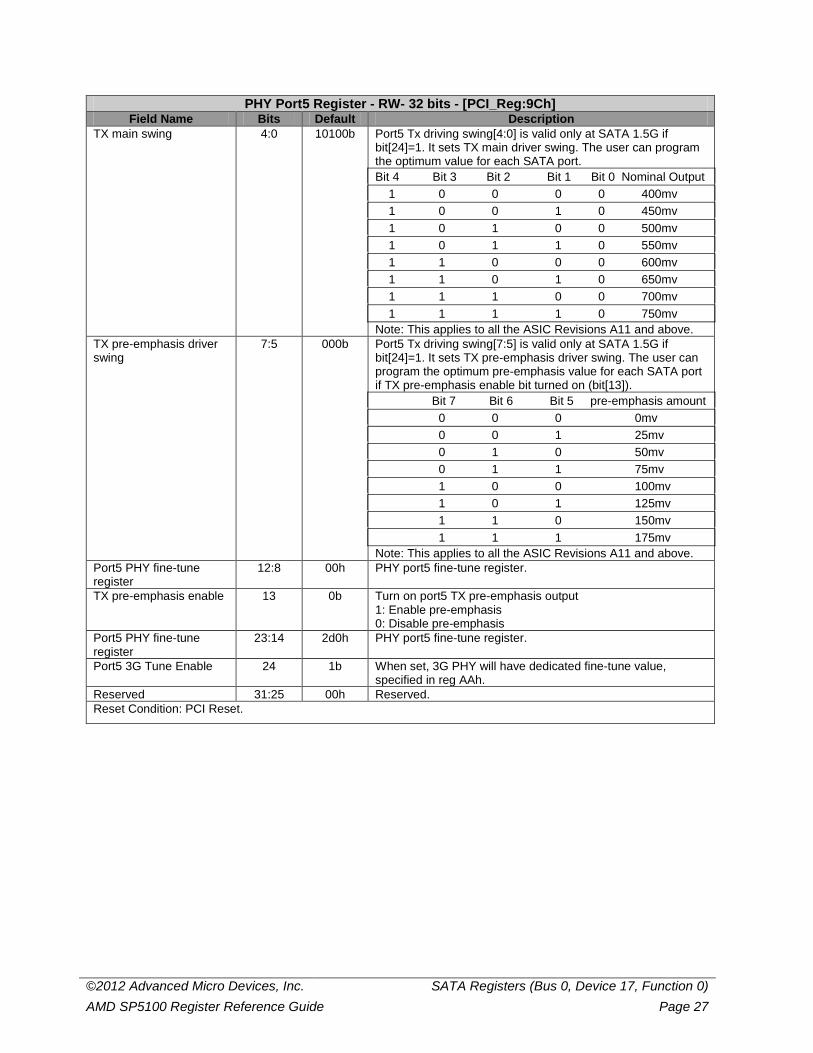
PHY Port5 Register - RW- 32 bits - [PCI_Reg:9Ch] Field Name Bits Default Description
TX main swing 4:0 10100b Port5 Tx driving swing[4:0] is valid only at SATA 1.5G if bit[24]=1. It sets TX main driver swing. The user can program the optimum value for each SATA port. Bit 4 Bit 3 Bit 2 Bit 1 Bit 0 Nominal Output 1 0 0 0 0 400mv 1 0 0 1 0 450mv 1 0 1 0 0 500mv 1 0 1 1 0 550mv 1 1 0 0 0 600mv 1 1 0 1 0 650mv 1 1 1 0 0 700mv 1 1 1 1 0 750mv Note: This applies to all the ASIC Revisions A11 and above.
TX pre-emphasis driver swing
7:5 000b Port5 Tx driving swing[7:5] is valid only at SATA 1.5G if bit[24]=1. It sets TX pre-emphasis driver swing. The user can program the optimum pre-emphasis value for each SATA port if TX pre-emphasis enable bit turned on (bit[13]). Bit 7 Bit 6 Bit 5 pre-emphasis amount 0 0 0 0mv 0 0 1 25mv 0 1 0 50mv 0 1 1 75mv 1 0 0 100mv 1 0 1 125mv 1 1 0 150mv 1 1 1 175mv Note: This applies to all the ASIC Revisions A11 and above.
Port5 PHY fine-tune register
12:8 00h PHY port5 fine-tune register.
TX pre-emphasis enable 13 0b Turn on port5 TX pre-emphasis output 1: Enable pre-emphasis 0: Disable pre-emphasis
Port5 PHY fine-tune register
23:14 2d0h PHY port5 fine-tune register.
Port5 3G Tune Enable 24 1b When set, 3G PHY will have dedicated fine-tune value, specified in reg AAh.
Reserved 31:25 00h Reserved. Reset Condition: PCI Reset.

©2012 Advanced Micro Devices, Inc. SATA Registers (Bus 0, Device 17, Function 0) AMD SP5100 Register Reference Guide Page 28
PHY Port0 GENII Register - RW- 16 bits - [PCI_Reg:A0h] Field Name Bits Default Description
TX main swing 4:0 10100b Port0 Tx driving swing[4:0] is valid only at SATA 3.0G. It sets TX main driver swing. The user can program the optimum value for each SATA port. Bit 4 Bit 3 Bit 2 Bit 1 Bit 0 Nominal Output 1 0 0 0 0 400mv 1 0 0 1 0 450mv 1 0 1 0 0 500mv 1 0 1 1 0 550mv 1 1 0 0 0 600mv 1 1 0 1 0 650mv 1 1 1 0 0 700mv 1 1 1 1 0 750mv Note: This applies to all the ASIC Revisions A11 and above.
TX pre-emphasis driver swing
7:5 000b Port0 Tx driving swing[7:5] is valid only at SATA 3.0G. It sets TX pre-emphasis driver swing. The user can program the optimum pre-emphasis value for each SATA port if TX pre-emphasis enable bit turned on (bit[13]). Bit 7 Bit 6 Bit 5 pre-emphasis amount 0 0 0 0mv 0 0 1 25mv 0 1 0 50mv 0 1 1 75mv 1 0 0 100mv 1 0 1 125mv 1 1 0 150mv 1 1 1 175mv Note: This applies to all the ASIC Revisions A11 and above.
Port0 PHY fine-tune register
12:8 00h PHY port0 fine-tune register.
TX pre-emphasis enable 13 0b Turn on port0 SATA 3.0G TX pre-emphasis output 1: Enable pre-emphasis 0: Disable pre-emphasis
Port0 PHY fine-tune register
15:14 0h PHY port0 fine-tune register.
Reset Condition: PCI Reset.
PHY Port1 GENII Register - RW- 16 bits - [PCI_Reg:A2h]
Field Name Bits Default Description TX main swing 4:0 10100b Port1 Tx driving swing[4:0] is valid only at SATA 3.0G. It sets
TX main driver swing. The user can program the optimum value for each SATA port. Bit 4 Bit 3 Bit 2 Bit 1 Bit 0 Nominal Output 1 0 0 0 0 400mv 1 0 0 1 0 450mv 1 0 1 0 0 500mv 1 0 1 1 0 550mv 1 1 0 0 0 600mv 1 1 0 1 0 650mv 1 1 1 0 0 700mv 1 1 1 1 0 750mv Note: This applies to all the ASIC Revisions A11 and above.
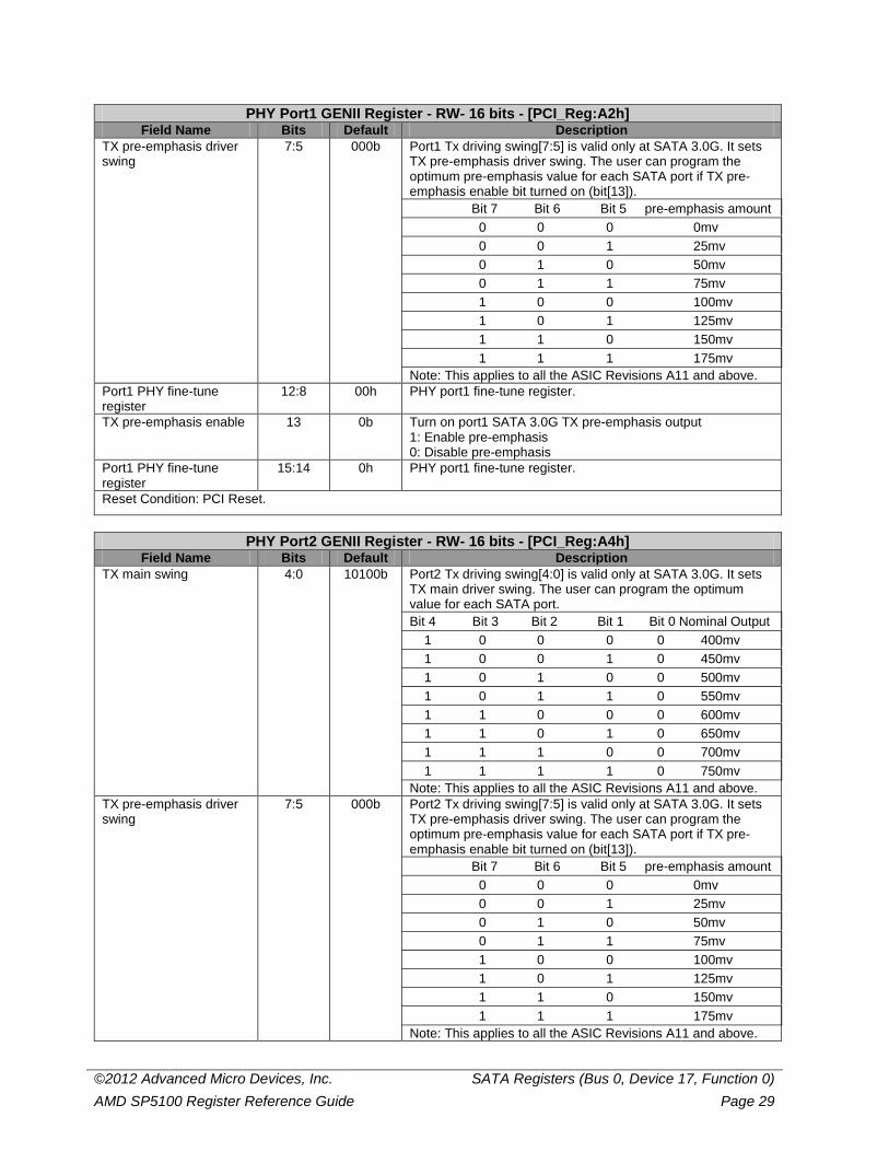
©2012 Advanced Micro Devices, Inc. SATA Registers (Bus 0, Device 17, Function 0) AMD SP5100 Register Reference Guide Page 29
PHY Port1 GENII Register - RW- 16 bits - [PCI_Reg:A2h] Field Name Bits Default Description
TX pre-emphasis driver swing
7:5 000b Port1 Tx driving swing[7:5] is valid only at SATA 3.0G. It sets TX pre-emphasis driver swing. The user can program the optimum pre-emphasis value for each SATA port if TX pre-emphasis enable bit turned on (bit[13]). Bit 7 Bit 6 Bit 5 pre-emphasis amount 0 0 0 0mv 0 0 1 25mv 0 1 0 50mv 0 1 1 75mv 1 0 0 100mv 1 0 1 125mv 1 1 0 150mv 1 1 1 175mv Note: This applies to all the ASIC Revisions A11 and above.
Port1 PHY fine-tune register
12:8 00h PHY port1 fine-tune register.
TX pre-emphasis enable 13 0b Turn on port1 SATA 3.0G TX pre-emphasis output 1: Enable pre-emphasis 0: Disable pre-emphasis
Port1 PHY fine-tune register
15:14 0h PHY port1 fine-tune register.
Reset Condition: PCI Reset.
PHY Port2 GENII Register - RW- 16 bits - [PCI_Reg:A4h]
Field Name Bits Default Description TX main swing 4:0 10100b Port2 Tx driving swing[4:0] is valid only at SATA 3.0G. It sets
TX main driver swing. The user can program the optimum value for each SATA port. Bit 4 Bit 3 Bit 2 Bit 1 Bit 0 Nominal Output 1 0 0 0 0 400mv 1 0 0 1 0 450mv 1 0 1 0 0 500mv 1 0 1 1 0 550mv 1 1 0 0 0 600mv 1 1 0 1 0 650mv 1 1 1 0 0 700mv 1 1 1 1 0 750mv Note: This applies to all the ASIC Revisions A11 and above.
TX pre-emphasis driver swing
7:5 000b Port2 Tx driving swing[7:5] is valid only at SATA 3.0G. It sets TX pre-emphasis driver swing. The user can program the optimum pre-emphasis value for each SATA port if TX pre-emphasis enable bit turned on (bit[13]). Bit 7 Bit 6 Bit 5 pre-emphasis amount 0 0 0 0mv 0 0 1 25mv 0 1 0 50mv 0 1 1 75mv 1 0 0 100mv 1 0 1 125mv 1 1 0 150mv 1 1 1 175mv Note: This applies to all the ASIC Revisions A11 and above.
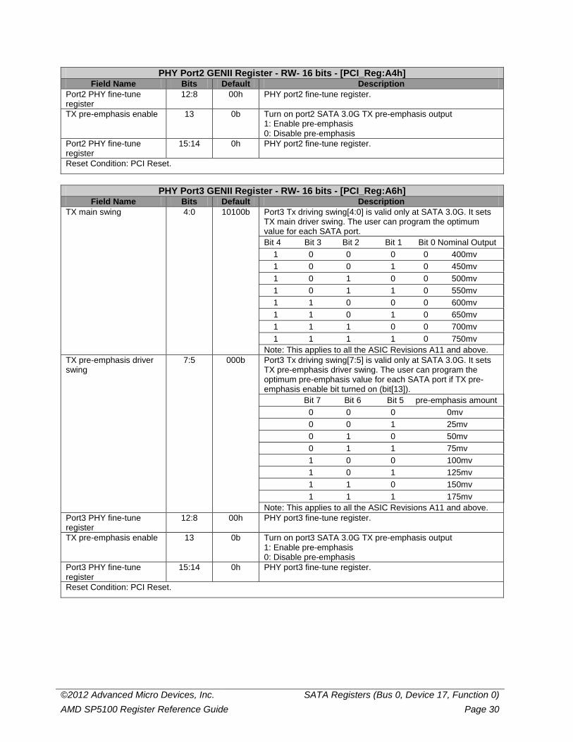
©2012 Advanced Micro Devices, Inc. SATA Registers (Bus 0, Device 17, Function 0) AMD SP5100 Register Reference Guide Page 30
PHY Port2 GENII Register - RW- 16 bits - [PCI_Reg:A4h] Field Name Bits Default Description
Port2 PHY fine-tune register
12:8 00h PHY port2 fine-tune register.
TX pre-emphasis enable 13 0b Turn on port2 SATA 3.0G TX pre-emphasis output 1: Enable pre-emphasis 0: Disable pre-emphasis
Port2 PHY fine-tune register
15:14 0h PHY port2 fine-tune register.
Reset Condition: PCI Reset.
PHY Port3 GENII Register - RW- 16 bits - [PCI_Reg:A6h]
Field Name Bits Default Description TX main swing 4:0 10100b Port3 Tx driving swing[4:0] is valid only at SATA 3.0G. It sets
TX main driver swing. The user can program the optimum value for each SATA port. Bit 4 Bit 3 Bit 2 Bit 1 Bit 0 Nominal Output 1 0 0 0 0 400mv 1 0 0 1 0 450mv 1 0 1 0 0 500mv 1 0 1 1 0 550mv 1 1 0 0 0 600mv 1 1 0 1 0 650mv 1 1 1 0 0 700mv 1 1 1 1 0 750mv Note: This applies to all the ASIC Revisions A11 and above.
TX pre-emphasis driver swing
7:5 000b Port3 Tx driving swing[7:5] is valid only at SATA 3.0G. It sets TX pre-emphasis driver swing. The user can program the optimum pre-emphasis value for each SATA port if TX pre-emphasis enable bit turned on (bit[13]). Bit 7 Bit 6 Bit 5 pre-emphasis amount 0 0 0 0mv 0 0 1 25mv 0 1 0 50mv 0 1 1 75mv 1 0 0 100mv 1 0 1 125mv 1 1 0 150mv 1 1 1 175mv Note: This applies to all the ASIC Revisions A11 and above.
Port3 PHY fine-tune register
12:8 00h PHY port3 fine-tune register.
TX pre-emphasis enable 13 0b Turn on port3 SATA 3.0G TX pre-emphasis output 1: Enable pre-emphasis 0: Disable pre-emphasis
Port3 PHY fine-tune register
15:14 0h PHY port3 fine-tune register.
Reset Condition: PCI Reset.
©2012 Advanced Micro Devices, Inc. SATA Registers (Bus 0, Device 17, Function 0) AMD SP5100 Register Reference Guide Page 31
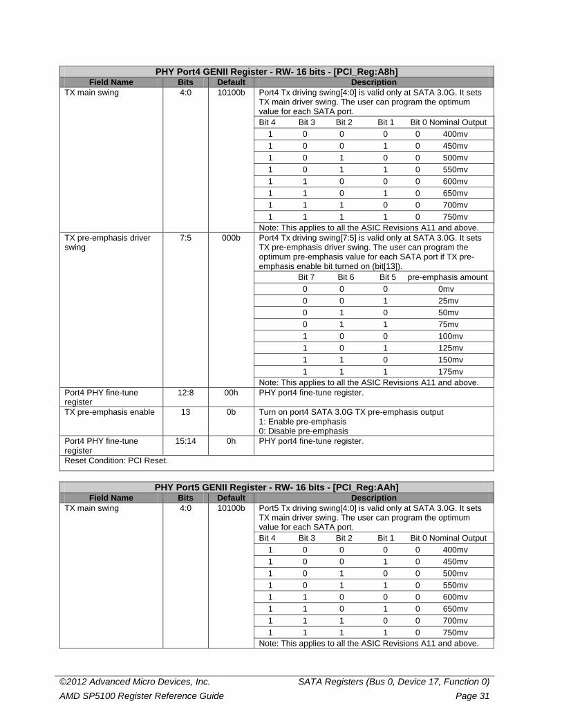
PHY Port4 GENII Register - RW- 16 bits - [PCI_Reg:A8h] Field Name Bits Default Description
TX main swing 4:0 10100b Port4 Tx driving swing[4:0] is valid only at SATA 3.0G. It sets TX main driver swing. The user can program the optimum value for each SATA port. Bit 4 Bit 3 Bit 2 Bit 1 Bit 0 Nominal Output 1 0 0 0 0 400mv 1 0 0 1 0 450mv 1 0 1 0 0 500mv 1 0 1 1 0 550mv 1 1 0 0 0 600mv 1 1 0 1 0 650mv 1 1 1 0 0 700mv 1 1 1 1 0 750mv Note: This applies to all the ASIC Revisions A11 and above.
TX pre-emphasis driver swing
7:5 000b Port4 Tx driving swing[7:5] is valid only at SATA 3.0G. It sets TX pre-emphasis driver swing. The user can program the optimum pre-emphasis value for each SATA port if TX pre-emphasis enable bit turned on (bit[13]). Bit 7 Bit 6 Bit 5 pre-emphasis amount 0 0 0 0mv 0 0 1 25mv 0 1 0 50mv 0 1 1 75mv 1 0 0 100mv 1 0 1 125mv 1 1 0 150mv 1 1 1 175mv Note: This applies to all the ASIC Revisions A11 and above.
Port4 PHY fine-tune register
12:8 00h PHY port4 fine-tune register.
TX pre-emphasis enable 13 0b Turn on port4 SATA 3.0G TX pre-emphasis output 1: Enable pre-emphasis 0: Disable pre-emphasis
Port4 PHY fine-tune register
15:14 0h PHY port4 fine-tune register.
Reset Condition: PCI Reset.
PHY Port5 GENII Register - RW- 16 bits - [PCI_Reg:AAh]
Field Name Bits Default Description TX main swing 4:0 10100b Port5 Tx driving swing[4:0] is valid only at SATA 3.0G. It sets
TX main driver swing. The user can program the optimum value for each SATA port. Bit 4 Bit 3 Bit 2 Bit 1 Bit 0 Nominal Output 1 0 0 0 0 400mv 1 0 0 1 0 450mv 1 0 1 0 0 500mv 1 0 1 1 0 550mv 1 1 0 0 0 600mv 1 1 0 1 0 650mv 1 1 1 0 0 700mv 1 1 1 1 0 750mv Note: This applies to all the ASIC Revisions A11 and above.
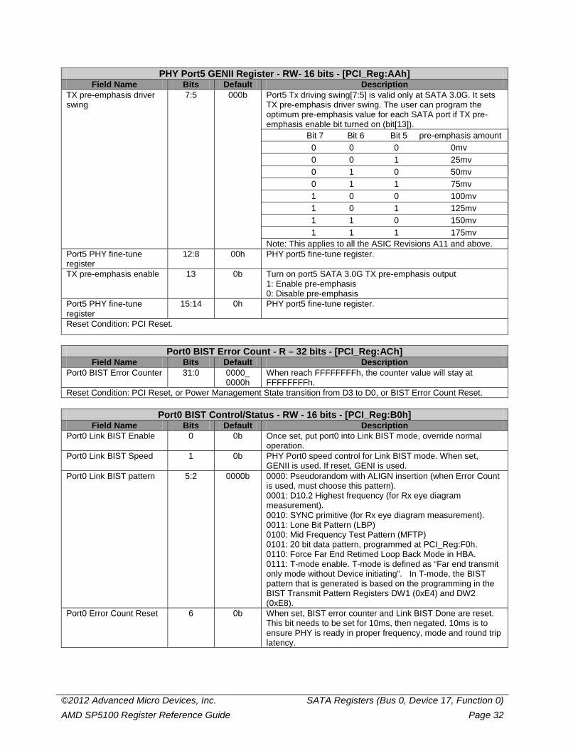
©2012 Advanced Micro Devices, Inc. SATA Registers (Bus 0, Device 17, Function 0) AMD SP5100 Register Reference Guide Page 32
PHY Port5 GENII Register - RW- 16 bits - [PCI_Reg:AAh] Field Name Bits Default Description
TX pre-emphasis driver swing
7:5 000b Port5 Tx driving swing[7:5] is valid only at SATA 3.0G. It sets TX pre-emphasis driver swing. The user can program the optimum pre-emphasis value for each SATA port if TX pre-emphasis enable bit turned on (bit[13]). Bit 7 Bit 6 Bit 5 pre-emphasis amount 0 0 0 0mv 0 0 1 25mv 0 1 0 50mv 0 1 1 75mv 1 0 0 100mv 1 0 1 125mv 1 1 0 150mv 1 1 1 175mv Note: This applies to all the ASIC Revisions A11 and above.
Port5 PHY fine-tune register
12:8 00h PHY port5 fine-tune register.
TX pre-emphasis enable 13 0b Turn on port5 SATA 3.0G TX pre-emphasis output 1: Enable pre-emphasis 0: Disable pre-emphasis
Port5 PHY fine-tune register
15:14 0h PHY port5 fine-tune register.
Reset Condition: PCI Reset.
Port0 BIST Error Count - R – 32 bits - [PCI_Reg:ACh]
Field Name Bits Default Description Port0 BIST Error Counter
31:0 0000_ 0000h
When reach FFFFFFFFh, the counter value will stay at FFFFFFFFh.
Reset Condition: PCI Reset, or Power Management State transition from D3 to D0, or BIST Error Count Reset.
Port0 BIST Control/Status - RW - 16 bits - [PCI_Reg:B0h] Field Name Bits Default Description
Port0 Link BIST Enable 0 0b Once set, put port0 into Link BIST mode, override normal operation.
Port0 Link BIST Speed 1 0b PHY Port0 speed control for Link BIST mode. When set, GENII is used. If reset, GENI is used.
Port0 Link BIST pattern 5:2 0000b 0000: Pseudorandom with ALIGN insertion (when Error Count is used, must choose this pattern). 0001: D10.2 Highest frequency (for Rx eye diagram measurement). 0010: SYNC primitive (for Rx eye diagram measurement). 0011: Lone Bit Pattern (LBP) 0100: Mid Frequency Test Pattern (MFTP) 0101: 20 bit data pattern, programmed at PCI_Reg:F0h. 0110: Force Far End Retimed Loop Back Mode in HBA. 0111: T-mode enable. T-mode is defined as “Far end transmit only mode without Device initiating”. In T-mode, the BIST pattern that is generated is based on the programming in the BIST Transmit Pattern Registers DW1 (0xE4) and DW2 (0xE8).
Port0 Error Count Reset 6 0b When set, BIST error counter and Link BIST Done are reset. This bit needs to be set for 10ms, then negated. 10ms is to ensure PHY is ready in proper frequency, mode and round trip latency.
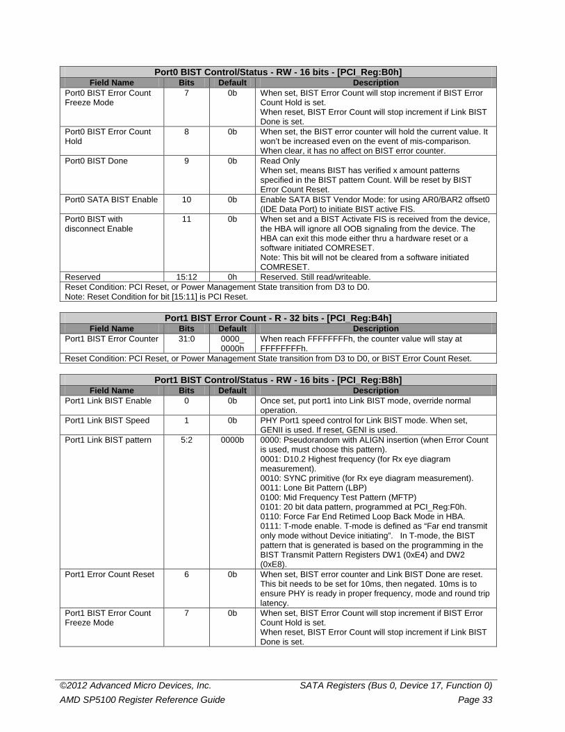
©2012 Advanced Micro Devices, Inc. SATA Registers (Bus 0, Device 17, Function 0) AMD SP5100 Register Reference Guide Page 33
Port0 BIST Control/Status - RW - 16 bits - [PCI_Reg:B0h] Field Name Bits Default Description
Port0 BIST Error Count Freeze Mode
7 0b When set, BIST Error Count will stop increment if BIST Error Count Hold is set. When reset, BIST Error Count will stop increment if Link BIST Done is set.
Port0 BIST Error Count Hold
8 0b When set, the BIST error counter will hold the current value. It won’t be increased even on the event of mis-comparison. When clear, it has no affect on BIST error counter.
Port0 BIST Done 9 0b Read Only When set, means BIST has verified x amount patterns specified in the BIST pattern Count. Will be reset by BIST Error Count Reset.
Port0 SATA BIST Enable 10 0b Enable SATA BIST Vendor Mode: for using AR0/BAR2 offset0 (IDE Data Port) to initiate BIST active FIS.
Port0 BIST with disconnect Enable
11 0b When set and a BIST Activate FIS is received from the device, the HBA will ignore all OOB signaling from the device. The HBA can exit this mode either thru a hardware reset or a software initiated COMRESET. Note: This bit will not be cleared from a software initiated COMRESET.
Reserved 15:12 0h Reserved. Still read/writeable. Reset Condition: PCI Reset, or Power Management State transition from D3 to D0. Note: Reset Condition for bit [15:11] is PCI Reset.
Port1 BIST Error Count - R - 32 bits - [PCI_Reg:B4h]
Field Name Bits Default Description Port1 BIST Error Counter 31:0 0000_
0000h When reach FFFFFFFFh, the counter value will stay at FFFFFFFFh.
Reset Condition: PCI Reset, or Power Management State transition from D3 to D0, or BIST Error Count Reset.
Port1 BIST Control/Status - RW - 16 bits - [PCI_Reg:B8h] Field Name Bits Default Description
Port1 Link BIST Enable 0 0b Once set, put port1 into Link BIST mode, override normal operation.
Port1 Link BIST Speed 1 0b PHY Port1 speed control for Link BIST mode. When set, GENII is used. If reset, GENI is used.
Port1 Link BIST pattern 5:2 0000b 0000: Pseudorandom with ALIGN insertion (when Error Count is used, must choose this pattern). 0001: D10.2 Highest frequency (for Rx eye diagram measurement). 0010: SYNC primitive (for Rx eye diagram measurement). 0011: Lone Bit Pattern (LBP) 0100: Mid Frequency Test Pattern (MFTP) 0101: 20 bit data pattern, programmed at PCI_Reg:F0h. 0110: Force Far End Retimed Loop Back Mode in HBA. 0111: T-mode enable. T-mode is defined as “Far end transmit only mode without Device initiating”. In T-mode, the BIST pattern that is generated is based on the programming in the BIST Transmit Pattern Registers DW1 (0xE4) and DW2 (0xE8).
Port1 Error Count Reset 6 0b When set, BIST error counter and Link BIST Done are reset. This bit needs to be set for 10ms, then negated. 10ms is to ensure PHY is ready in proper frequency, mode and round trip latency.
Port1 BIST Error Count Freeze Mode
7 0b When set, BIST Error Count will stop increment if BIST Error Count Hold is set. When reset, BIST Error Count will stop increment if Link BIST Done is set.
©2012 Advanced Micro Devices, Inc. SATA Registers (Bus 0, Device 17, Function 0) AMD SP5100 Register Reference Guide Page 34
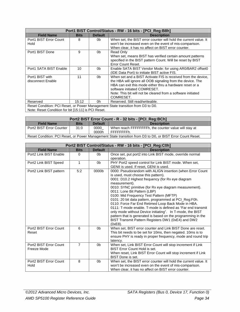
Port1 BIST Control/Status - RW - 16 bits - [PCI_Reg:B8h] Field Name Bits Default Description
Port1 BIST Error Count Hold
8 0b When set, the BIST error counter will hold the current value. It won’t be increased even on the event of mis-comparison. When clear, it has no affect on BIST error counter.
Port1 BIST Done 9 0b Read Only When set, means BIST has verified certain amount patterns specified in the BIST pattern Count. Will be reset by BIST Error Count Reset.
Port1 SATA BIST Enable 10 0b Enable SATA BIST Vendor Mode: for using AR0/BAR2 offset0 (IDE Data Port) to initiate BIST active FIS.
Port1 BIST with disconnect Enable
11 0b When set and a BIST Activate FIS is received from the device, the HBA will ignore all OOB signaling from the device. The HBA can exit this mode either thru a hardware reset or a software initiated COMRESET. Note: This bit will not be cleared from a software initiated COMRESET.
Reserved 15:12 0h Reserved. Still read/writeable. Reset Condition: PCI Reset, or Power Management State transition from D3 to D0. Note: Reset Condition for bit [15:11] is PCI Reset.
Port2 BIST Error Count - R - 32 bits - [PCI_Reg:BCh]
Field Name Bits Default Description Port2 BIST Error Counter 31:0 0000_
0000h When reach FFFFFFFFh, the counter value will stay at FFFFFFFFh.
Reset Condition: PCI Reset, or Power Management State transition from D3 to D0, or BIST Error Count Reset.
Port2 BIST Control/Status - RW - 16 bits - [PCI_Reg:C0h] Field Name Bits Default Description
Port2 Link BIST Enable 0 0b Once set, put port2 into Link BIST mode, override normal operation.
Port2 Link BIST Speed 1 0b PHY Port2 speed control for Link BIST mode. When set, GENII is used. If reset, GENI is used.
Port2 Link BIST pattern 5:2 0000b 0000: Pseudorandom with ALIGN insertion (when Error Count is used, must choose this pattern). 0001: D10.2 Highest frequency (for Rx eye diagram measurement). 0010: SYNC primitive (for Rx eye diagram measurement). 0011: Lone Bit Pattern (LBP) 0100: Mid Frequency Test Pattern (MFTP) 0101: 20 bit data pattern, programmed at PCI_Reg:F0h. 0110: Force Far End Retimed Loop Back Mode in HBA. 0111: T-mode enable. T-mode is defined as “Far end transmit only mode without Device initiating”. In T-mode, the BIST pattern that is generated is based on the programming in the BIST Transmit Pattern Registers DW1 (0xE4) and DW2 (0xE8).
Port2 BIST Error Count Reset
6 0b When set, BIST error counter and Link BIST Done are reset. This bit needs to be set for 10ms, then negated. 10ms is to ensure PHY is ready in proper frequency, mode and round trip latency.
Port2 BIST Error Count Freeze Mode
7 0b When set, Link BIST Error Count will stop increment if Link BIST Error Count Hold is set. When reset, Link BIST Error Count will stop increment if Link BIST Done is set.
Port2 BIST Error Count Hold
8 0b When set, the BIST error counter will hold the current value. It won’t be increased even on the event of mis-comparison. When clear, it has no affect on BIST error counter.
©2012 Advanced Micro Devices, Inc. SATA Registers (Bus 0, Device 17, Function 0) AMD SP5100 Register Reference Guide Page 35
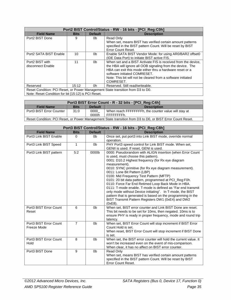
Port2 BIST Control/Status - RW - 16 bits - [PCI_Reg:C0h] Field Name Bits Default Description
Port2 BIST Done 9 0b Read Only When set, means BIST has verified certain amount patterns specified in the BIST pattern Count. Will be reset by BIST Error Count Reset.
Port2 SATA BIST Enable 10 0b Enable SATA BIST Vendor Mode: for using AR0/BAR2 offset0 (IDE Data Port) to initiate BIST active FIS.
Port2 BIST with disconnect Enable
11 0b When set and a BIST Activate FIS is received from the device, the HBA will ignore all OOB signaling from the device. The HBA can exit this mode either thru a hardware reset or a software initiated COMRESET. Note: This bit will not be cleared from a software initiated COMRESET.
Reserved 15:12 0h Reserved. Still read/writeable. Reset Condition: PCI Reset, or Power Management State transition from D3 to D0. Note: Reset Condition for bit [15:12] is PCI Reset.
Port3 BIST Error Count - R - 32 bits - [PCI_Reg:C4h]
Field Name Bits Default Description Port3 BIST Error Counter 31:0 0000_
0000h When reach FFFFFFFFh, the counter value will stay at FFFFFFFFh.
Reset Condition: PCI Reset, or Power Management State transition from D3 to D0, or BIST Error Count Reset.
Port3 BIST Control/Status - RW - 16 bits - [PCI_Reg:C8h] Field Name Bits Default Description
Port3 Link BIST Enable 0 0b Once set, put port3 into Link BIST mode, override normal operation.
Port3 Link BIST Speed 1 0b PHY Port3 speed control for Link BIST mode. When set, GENII is used. If reset, GENI is used.
Port3 Link BIST pattern 5:2 0000b 0000: Pseudorandom with ALIGN insertion (when Error Count is used, must choose this pattern). 0001: D10.2 Highest frequency (for Rx eye diagram measurement). 0010: SYNC primitive (for Rx eye diagram measurement). 0011: Lone Bit Pattern (LBP) 0100: Mid Frequency Test Pattern (MFTP) 0101: 20 bit data pattern, programmed at PCI_Reg:F0h. 0110: Force Far End Retimed Loop Back Mode in HBA. 0111: T-mode enable. T-mode is defined as “Far end transmit only mode without Device initiating”. In T-mode, the BIST pattern that is generated is based on the programming in the BIST Transmit Pattern Registers DW1 (0xE4) and DW2 (0xE8).
Port3 BIST Error Count Reset
6 0b When set, BIST error counter and Link BIST Done are reset. This bit needs to be set for 10ms, then negated. 10ms is to ensure PHY is ready in proper frequency, mode and round trip latency.
Port3 BIST Error Count Freeze Mode
7 0b When set, BIST Error Count will stop increment if BIST Error Count Hold is set. When reset, BIST Error Count will stop increment if BIST Done is set.
Port3 BIST Error Count Hold
8 0b When set, the BIST error counter will hold the current value. It won’t be increased even on the event of mis-comparison. When clear, it has no affect on BIST error counter.
Port3 BIST Done 9 0b Read Only When set, means BIST has verified certain amount patterns specified in the BIST pattern Count. Will be reset by BIST Error Count Reset.
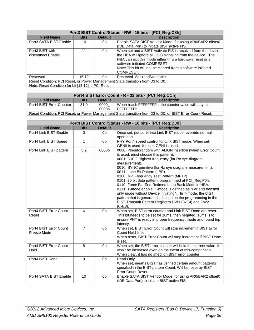
©2012 Advanced Micro Devices, Inc. SATA Registers (Bus 0, Device 17, Function 0) AMD SP5100 Register Reference Guide Page 36
Port3 BIST Control/Status - RW - 16 bits - [PCI_Reg:C8h] Field Name Bits Default Description
Port3 SATA BIST Enable 10 0b Enable SATA BIST Vendor Mode: for using AR0/BAR2 offset0 (IDE Data Port) to initiate BIST active FIS.
Port3 BIST with disconnect Enable
11 0b When set and a BIST Activate FIS is received from the device, the HBA will ignore all OOB signaling from the device. The HBA can exit this mode either thru a hardware reset or a software initiated COMRESET. Note: This bit will not be cleared from a software initiated COMRESET.
Reserved 15:12 0h Reserved. Still read/writeable. Reset Condition: PCI Reset, or Power Management State transition from D3 to D0. Note: Reset Condition for bit [15:12] is PCI Reset.
Port4 BIST Error Count - R - 32 bits - [PCI_Reg:CCh]
Field Name Bits Default Description Port4 BIST Error Counter 31:0 0000_
0000h When reach FFFFFFFFh, the counter value will stay at FFFFFFFFh.
Reset Condition: PCI Reset, or Power Management State transition from D3 to D0, or BIST Error Count Reset.
Port4 BIST Control/Status - RW - 16 bits - [PCI_Reg:D0h] Field Name Bits Default Description
Port4 Link BIST Enable 0 0b Once set, put port4 into Link BIST mode, override normal operation.
Port4 Link BIST Speed 1 0b PHY Port4 speed control for Link BIST mode. When set, GENII is used. If reset, GENI is used.
Port4 Link BIST pattern 5:2 0000b 0000: Pseudorandom with ALIGN insertion (when Error Count is used, must choose this pattern). 0001: D10.2 Highest frequency (for Rx eye diagram measurement). 0010: SYNC primitive (for Rx eye diagram measurement). 0011: Lone Bit Pattern (LBP) 0100: Mid Frequency Test Pattern (MFTP) 0101: 20 bit data pattern, programmed at PCI_Reg:F0h. 0110: Force Far End Retimed Loop Back Mode in HBA. 0111: T-mode enable. T-mode is defined as “Far end transmit only mode without Device initiating”. In T-mode, the BIST pattern that is generated is based on the programming in the BIST Transmit Pattern Registers DW1 (0xE4) and DW2 (0xE8).
Port4 BIST Error Count Reset
6 0b When set, BIST error counter and Link BIST Done are reset. This bit needs to be set for 10ms, then negated. 10ms is to ensure PHY is ready in proper frequency, mode and round trip latency.
Port4 BIST Error Count Freeze Mode
7 0b When set, BIST Error Count will stop increment if BIST Error Count Hold is set. When reset, BIST Error Count will stop increment if BIST Done is set.
Port4 BIST Error Count Hold
8 0b When set, the BIST error counter will hold the current value. It won’t be increased even on the event of mis-comparison. When clear, it has no affect on BIST error counter.
Port4 BIST Done 9 0b Read Only When set, means BIST has verified certain amount patterns specified in the BIST pattern Count. Will be reset by BIST Error Count Reset.
Port4 SATA BIST Enable 10 0b Enable SATA BIST Vendor Mode: for using AR0/BAR2 offset0 (IDE Data Port) to initiate BIST active FIS.
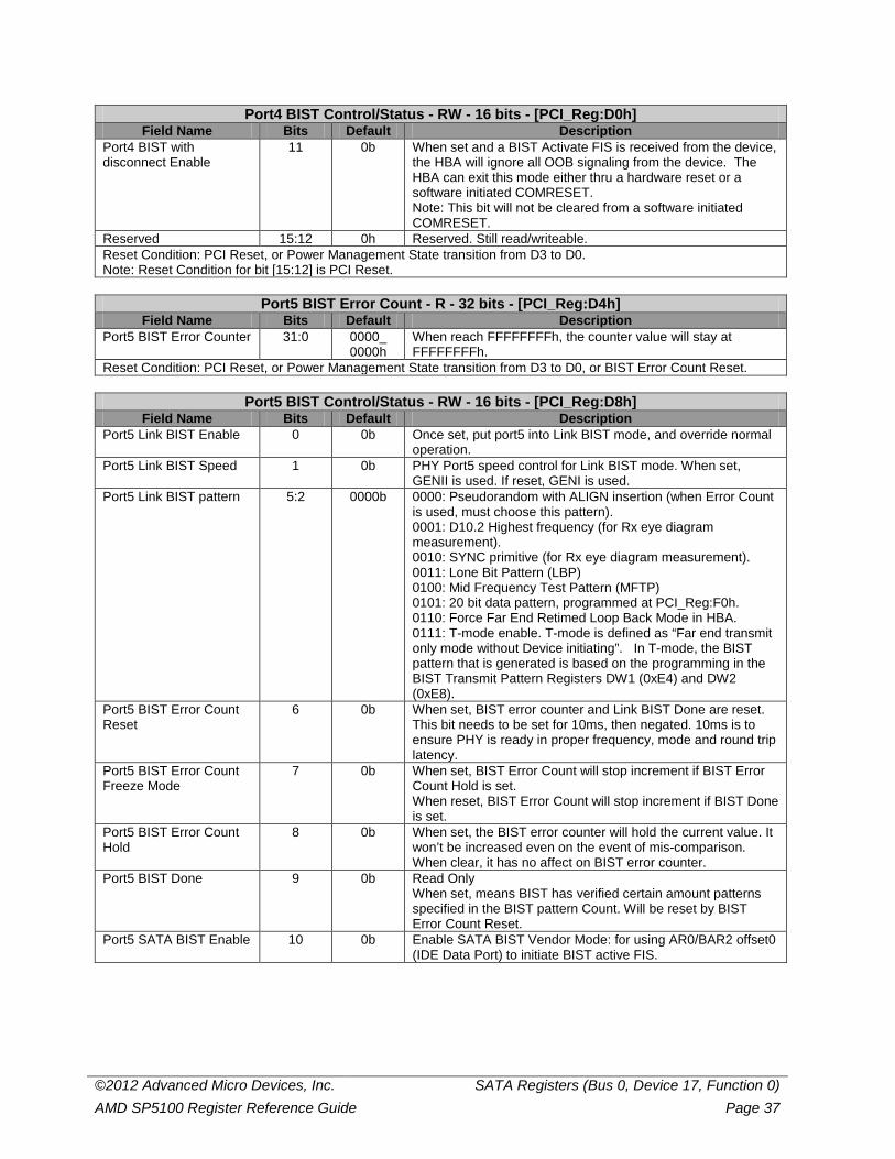
©2012 Advanced Micro Devices, Inc. SATA Registers (Bus 0, Device 17, Function 0) AMD SP5100 Register Reference Guide Page 37
Port4 BIST Control/Status - RW - 16 bits - [PCI_Reg:D0h] Field Name Bits Default Description
Port4 BIST with disconnect Enable
11 0b When set and a BIST Activate FIS is received from the device, the HBA will ignore all OOB signaling from the device. The HBA can exit this mode either thru a hardware reset or a software initiated COMRESET. Note: This bit will not be cleared from a software initiated COMRESET.
Reserved 15:12 0h Reserved. Still read/writeable. Reset Condition: PCI Reset, or Power Management State transition from D3 to D0. Note: Reset Condition for bit [15:12] is PCI Reset.
Port5 BIST Error Count - R - 32 bits - [PCI_Reg:D4h]
Field Name Bits Default Description Port5 BIST Error Counter 31:0 0000_
0000h When reach FFFFFFFFh, the counter value will stay at FFFFFFFFh.
Reset Condition: PCI Reset, or Power Management State transition from D3 to D0, or BIST Error Count Reset.
Port5 BIST Control/Status - RW - 16 bits - [PCI_Reg:D8h] Field Name Bits Default Description
Port5 Link BIST Enable 0 0b Once set, put port5 into Link BIST mode, and override normal operation.
Port5 Link BIST Speed 1 0b PHY Port5 speed control for Link BIST mode. When set, GENII is used. If reset, GENI is used.
Port5 Link BIST pattern 5:2 0000b 0000: Pseudorandom with ALIGN insertion (when Error Count is used, must choose this pattern). 0001: D10.2 Highest frequency (for Rx eye diagram measurement). 0010: SYNC primitive (for Rx eye diagram measurement). 0011: Lone Bit Pattern (LBP) 0100: Mid Frequency Test Pattern (MFTP) 0101: 20 bit data pattern, programmed at PCI_Reg:F0h. 0110: Force Far End Retimed Loop Back Mode in HBA. 0111: T-mode enable. T-mode is defined as “Far end transmit only mode without Device initiating”. In T-mode, the BIST pattern that is generated is based on the programming in the BIST Transmit Pattern Registers DW1 (0xE4) and DW2 (0xE8).
Port5 BIST Error Count Reset
6 0b When set, BIST error counter and Link BIST Done are reset. This bit needs to be set for 10ms, then negated. 10ms is to ensure PHY is ready in proper frequency, mode and round trip latency.
Port5 BIST Error Count Freeze Mode
7 0b When set, BIST Error Count will stop increment if BIST Error Count Hold is set. When reset, BIST Error Count will stop increment if BIST Done is set.
Port5 BIST Error Count Hold
8 0b When set, the BIST error counter will hold the current value. It won’t be increased even on the event of mis-comparison. When clear, it has no affect on BIST error counter.
Port5 BIST Done 9 0b Read Only When set, means BIST has verified certain amount patterns specified in the BIST pattern Count. Will be reset by BIST Error Count Reset.
Port5 SATA BIST Enable 10 0b Enable SATA BIST Vendor Mode: for using AR0/BAR2 offset0 (IDE Data Port) to initiate BIST active FIS.
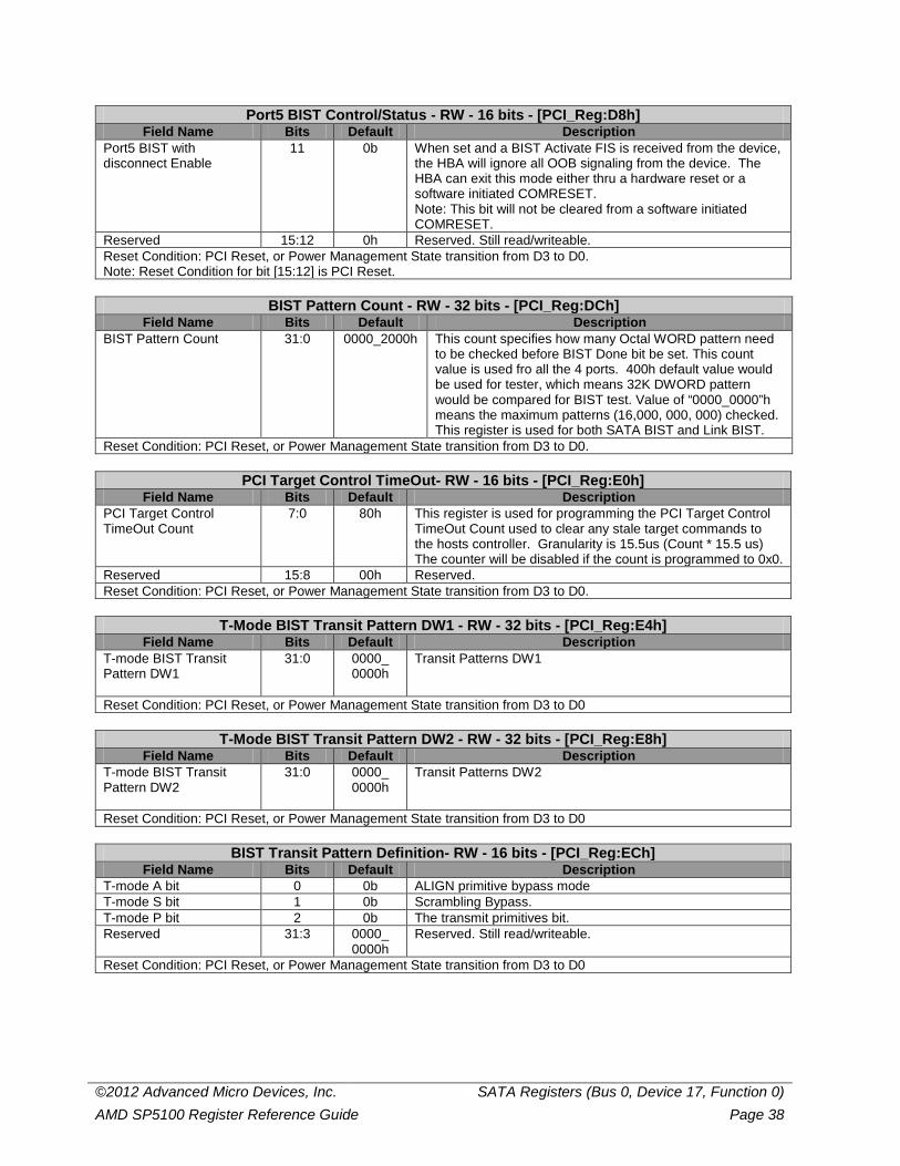
©2012 Advanced Micro Devices, Inc. SATA Registers (Bus 0, Device 17, Function 0) AMD SP5100 Register Reference Guide Page 38
Port5 BIST Control/Status - RW - 16 bits - [PCI_Reg:D8h] Field Name Bits Default Description
Port5 BIST with disconnect Enable
11 0b When set and a BIST Activate FIS is received from the device, the HBA will ignore all OOB signaling from the device. The HBA can exit this mode either thru a hardware reset or a software initiated COMRESET. Note: This bit will not be cleared from a software initiated COMRESET.
Reserved 15:12 0h Reserved. Still read/writeable. Reset Condition: PCI Reset, or Power Management State transition from D3 to D0. Note: Reset Condition for bit [15:12] is PCI Reset.
BIST Pattern Count - RW - 32 bits - [PCI_Reg:DCh]
Field Name Bits Default Description BIST Pattern Count 31:0 0000_2000h This count specifies how many Octal WORD pattern need
to be checked before BIST Done bit be set. This count value is used fro all the 4 ports. 400h default value would be used for tester, which means 32K DWORD pattern would be compared for BIST test. Value of “0000_0000”h means the maximum patterns (16,000, 000, 000) checked. This register is used for both SATA BIST and Link BIST.
Reset Condition: PCI Reset, or Power Management State transition from D3 to D0.
PCI Target Control TimeOut- RW - 16 bits - [PCI_Reg:E0h] Field Name Bits Default Description
PCI Target Control TimeOut Count
7:0 80h This register is used for programming the PCI Target Control TimeOut Count used to clear any stale target commands to the hosts controller. Granularity is 15.5us (Count * 15.5 us) The counter will be disabled if the count is programmed to 0x0.
Reserved 15:8 00h Reserved. Reset Condition: PCI Reset, or Power Management State transition from D3 to D0.
T-Mode BIST Transit Pattern DW1 - RW - 32 bits - [PCI_Reg:E4h]
Field Name Bits Default Description T-mode BIST Transit Pattern DW1
31:0 0000_ 0000h
Transit Patterns DW1
Reset Condition: PCI Reset, or Power Management State transition from D3 to D0
T-Mode BIST Transit Pattern DW2 - RW - 32 bits - [PCI_Reg:E8h] Field Name Bits Default Description
T-mode BIST Transit Pattern DW2
31:0 0000_ 0000h
Transit Patterns DW2
Reset Condition: PCI Reset, or Power Management State transition from D3 to D0
BIST Transit Pattern Definition- RW - 16 bits - [PCI_Reg:ECh] Field Name Bits Default Description
T-mode A bit 0 0b ALIGN primitive bypass mode T-mode S bit 1 0b Scrambling Bypass. T-mode P bit 2 0b The transmit primitives bit. Reserved 31:3 0000_
0000h Reserved. Still read/writeable.
Reset Condition: PCI Reset, or Power Management State transition from D3 to D0
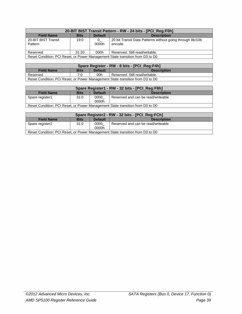
©2012 Advanced Micro Devices, Inc. SATA Registers (Bus 0, Device 17, Function 0) AMD SP5100 Register Reference Guide Page 39
20-BIT BIST Transit Pattern - RW - 24 bits - [PCI_Reg:F0h] Field Name Bits Default Description
20-BIT BIST Transit Pattern
19:0 0_ 0000h
20 bit Transit Data Patterns without going through 8b/10b encode.
Reserved 31:20 000h Reserved. Still read/writable. Reset Condition: PCI Reset, or Power Management State transition from D3 to D0
Spare Register - RW - 8 bits - [PCI_Reg:F4h]
Field Name Bits Default Description Reserved 7:0 00h Reserved. Still read/writable. Reset Condition: PCI Reset, or Power Management State transition from D3 to D0
Spare Register1 - RW - 32 bits - [PCI_Reg:F8h]
Field Name Bits Default Description Spare register1
31:0 0000_ 0000h
Reserved and can be read/writeable
Reset Condition: PCI Reset, or Power Management State transition from D3 to D0
Spare Register2 - RW - 32 bits - [PCI_Reg:FCh] Field Name Bits Default Description
Spare register2
31:0 0000_ 0000h
Reserved and can be read/writeable
Reset Condition: PCI Reset, or Power Management State transition from D3 to D0
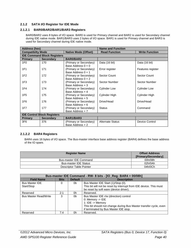
©2012 Advanced Micro Devices, Inc. SATA Registers (Bus 0, Device 17, Function 0) AMD SP5100 Register Reference Guide Page 40
2.1.2 SATA I/O Register for IDE Mode
2.1.2.1 BAR0/BAR2/BAR1/BAR3 Registers BAR0/BAR2 uses 8 bytes of I/O space. BAR0 is used for Primary channel and BAR2 is used for Secondary channel during IDE native mode. BAR1/BAR3 uses 2 bytes of I/O space. BAR1 is used for Primary channel and BAR3 is used for Secondary channel during IDE native mode.
Address (hex) Name and Function Compatibilty Mode Native Mode (Offset) Read Function Write Function IDE Command Block Registers Primary Secondary BAR0/BAR2 1F0 170 (Primary or Secondary)
Base Address 0 + 0 Data (16 bit) Data (16 bit)
1F1 171 (Primary or Secondary) Base Address 0 + 1
Error register Features register
1F2 172 (Primary or Secondary) Base Address 0 + 2
Sector Count Sector Count
1F3 173 (Primary or Secondary) Base Address + 3
Sector Number Sector Number
1F4 174 (Primary or Secondary) Base Address + 4
Cylinder Low Cylinder Low
1F5 175 (Primary or Secondary) Base Address + 5
Cylinder High Cylinder High
1F6 176 (Primary or Secondary) Base Address + 6
Drive/Head Drive/Head
1F7 177 (Primary or Secondary) Base Address + 7
Status Command
IDE Control Block Registers Primary Secondary BAR1/BAR3 3F6 376 (Primary or Secondary)
Base Address + 2 Alternate Status Device Control
2.1.2.2 BAR4 Registers BAR4 uses 16 bytes of I/O space. The Bus-master interface base address register (BAR4) defines the base address of the IO spare.
Register Name Offset Address [Primary/Secondary]
Bus-master IDE Command 00h/08h Bus-master IDE Status 02h/0Ah
Descriptor Table Pointer 04h/0Ch
Bus-master IDE Command - RW- 8 bits - [IO_Reg: BAR4 + 00/08h] Field Name Bits Default Description
Bus Master IDE Start/Stop
0 0b Bus Master IDE Start (1)/Stop (0). This bit will not be reset by interrupt from IDE device. This must be reset by soft ware (device driver).
Reserved 2:1 0h Reserved. Bus Master Read/Write 3 0b Bus Master IDE r/w (direction) control
0: Memory -> IDE 1: IDE -> Memory This bit should not change during Bus Master transfer cycle, even if terminated by Bus Master IDE stop.
Reserved 7:4 0h Reserved.
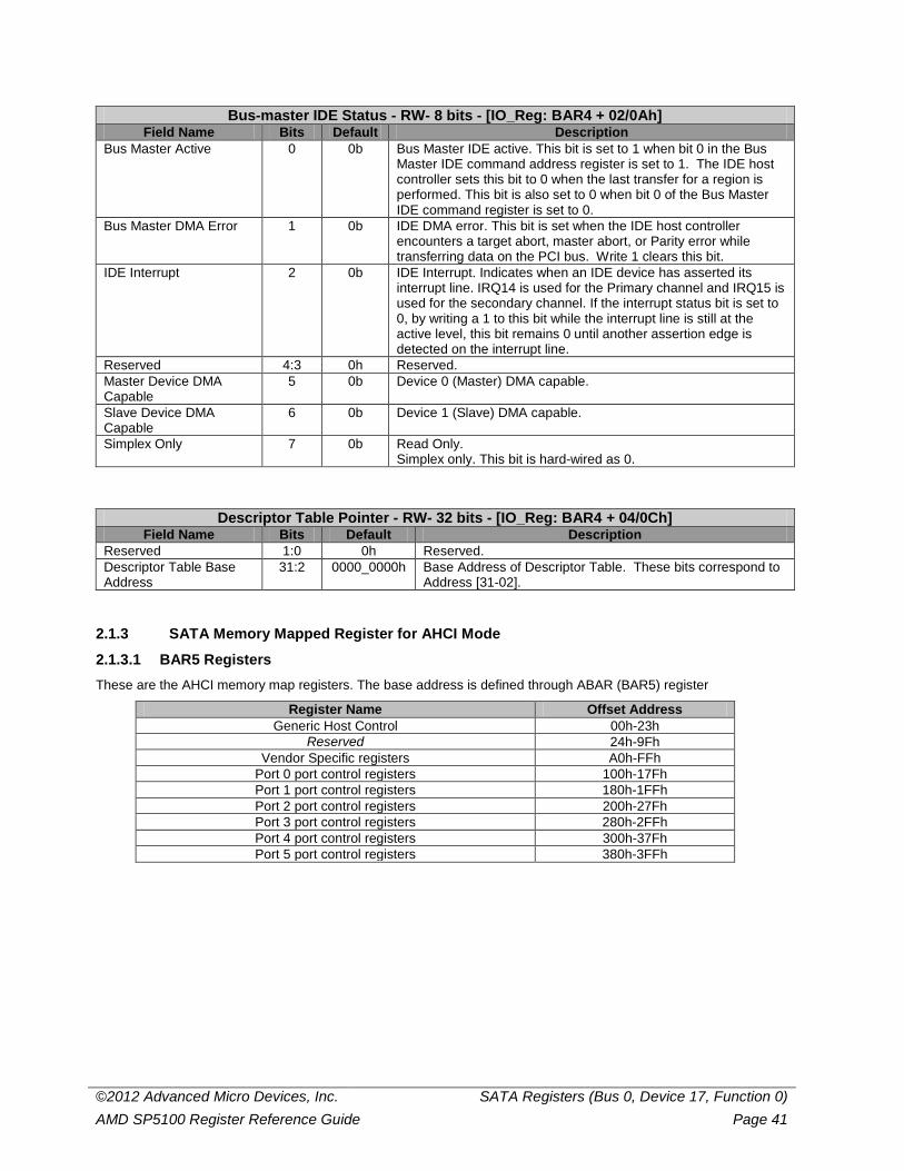
©2012 Advanced Micro Devices, Inc. SATA Registers (Bus 0, Device 17, Function 0) AMD SP5100 Register Reference Guide Page 41
Bus-master IDE Status - RW- 8 bits - [IO_Reg: BAR4 + 02/0Ah] Field Name Bits Default Description
Bus Master Active 0 0b Bus Master IDE active. This bit is set to 1 when bit 0 in the Bus Master IDE command address register is set to 1. The IDE host controller sets this bit to 0 when the last transfer for a region is performed. This bit is also set to 0 when bit 0 of the Bus Master IDE command register is set to 0.
Bus Master DMA Error 1 0b IDE DMA error. This bit is set when the IDE host controller encounters a target abort, master abort, or Parity error while transferring data on the PCI bus. Write 1 clears this bit.
IDE Interrupt 2 0b IDE Interrupt. Indicates when an IDE device has asserted its interrupt line. IRQ14 is used for the Primary channel and IRQ15 is used for the secondary channel. If the interrupt status bit is set to 0, by writing a 1 to this bit while the interrupt line is still at the active level, this bit remains 0 until another assertion edge is detected on the interrupt line.
Reserved 4:3 0h Reserved. Master Device DMA Capable
5 0b Device 0 (Master) DMA capable.
Slave Device DMA Capable
6 0b Device 1 (Slave) DMA capable.
Simplex Only 7 0b Read Only. Simplex only. This bit is hard-wired as 0.
Descriptor Table Pointer - RW- 32 bits - [IO_Reg: BAR4 + 04/0Ch] Field Name Bits Default Description
Reserved 1:0 0h Reserved. Descriptor Table Base Address
31:2 0000_0000h Base Address of Descriptor Table. These bits correspond to Address [31-02].
2.1.3 SATA Memory Mapped Register for AHCI Mode
2.1.3.1 BAR5 Registers These are the AHCI memory map registers. The base address is defined through ABAR (BAR5) register
Register Name Offset Address Generic Host Control 00h-23h
Reserved 24h-9Fh Vendor Specific registers A0h-FFh
Port 0 port control registers 100h-17Fh Port 1 port control registers 180h-1FFh Port 2 port control registers 200h-27Fh Port 3 port control registers 280h-2FFh Port 4 port control registers 300h-37Fh Port 5 port control registers 380h-3FFh
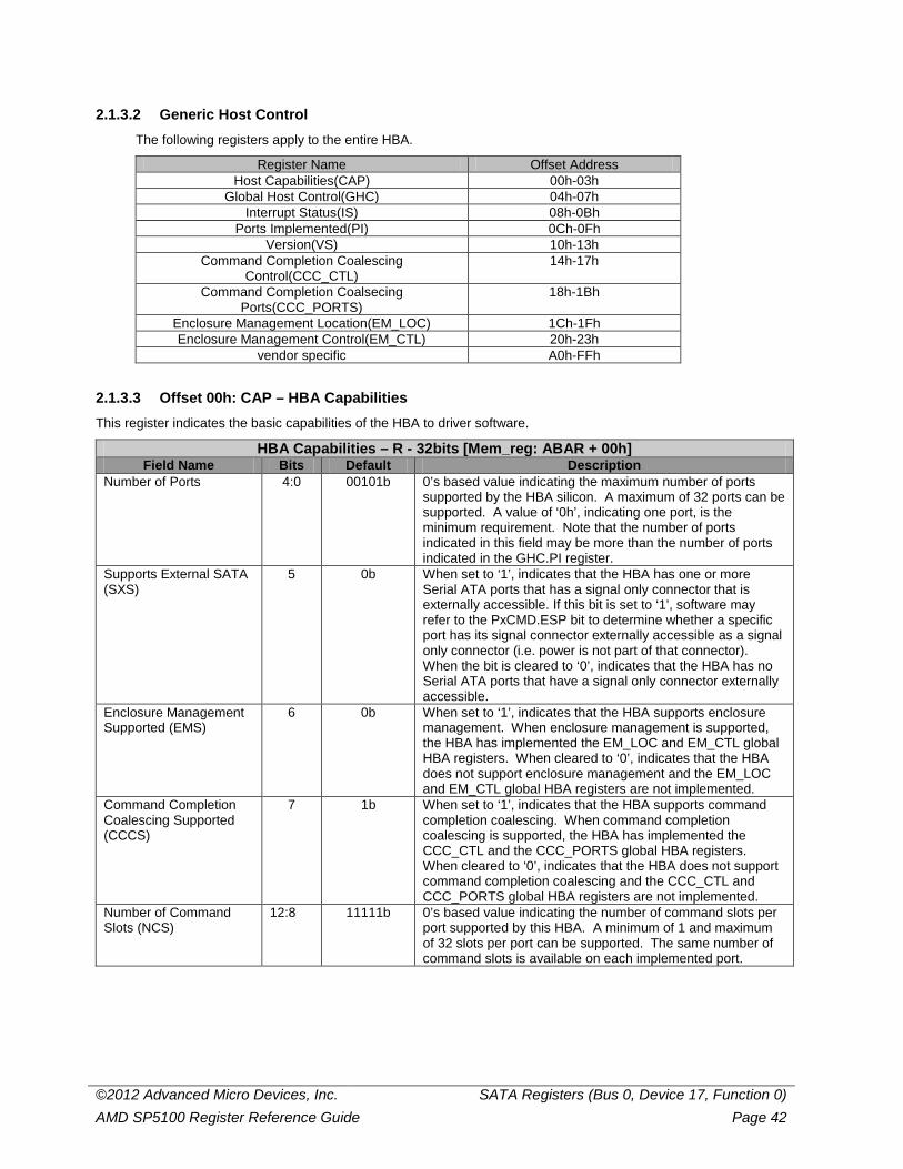
©2012 Advanced Micro Devices, Inc. SATA Registers (Bus 0, Device 17, Function 0) AMD SP5100 Register Reference Guide Page 42
2.1.3.2 Generic Host Control The following registers apply to the entire HBA.
Register Name Offset Address Host Capabilities(CAP) 00h-03h
Global Host Control(GHC) 04h-07h Interrupt Status(IS) 08h-0Bh
Ports Implemented(PI) 0Ch-0Fh Version(VS) 10h-13h
Command Completion Coalescing Control(CCC_CTL)
14h-17h
Command Completion Coalsecing Ports(CCC_PORTS)
18h-1Bh
Enclosure Management Location(EM_LOC) 1Ch-1Fh Enclosure Management Control(EM_CTL) 20h-23h
vendor specific A0h-FFh
2.1.3.3 Offset 00h: CAP – HBA Capabilities This register indicates the basic capabilities of the HBA to driver software.
HBA Capabilities – R - 32bits [Mem_reg: ABAR + 00h] Field Name Bits Default Description
Number of Ports 4:0 00101b 0’s based value indicating the maximum number of ports supported by the HBA silicon. A maximum of 32 ports can be supported. A value of ‘0h’, indicating one port, is the minimum requirement. Note that the number of ports indicated in this field may be more than the number of ports indicated in the GHC.PI register.
Supports External SATA (SXS)
5 0b When set to ‘1’, indicates that the HBA has one or more Serial ATA ports that has a signal only connector that is externally accessible. If this bit is set to ‘1’, software may refer to the PxCMD.ESP bit to determine whether a specific port has its signal connector externally accessible as a signal only connector (i.e. power is not part of that connector). When the bit is cleared to ‘0’, indicates that the HBA has no Serial ATA ports that have a signal only connector externally accessible.
Enclosure Management Supported (EMS)
6 0b When set to ‘1’, indicates that the HBA supports enclosure management. When enclosure management is supported, the HBA has implemented the EM_LOC and EM_CTL global HBA registers. When cleared to ‘0’, indicates that the HBA does not support enclosure management and the EM_LOC and EM_CTL global HBA registers are not implemented.
Command Completion Coalescing Supported (CCCS)
7 1b When set to ‘1’, indicates that the HBA supports command completion coalescing. When command completion coalescing is supported, the HBA has implemented the CCC_CTL and the CCC_PORTS global HBA registers. When cleared to ‘0’, indicates that the HBA does not support command completion coalescing and the CCC_CTL and CCC_PORTS global HBA registers are not implemented.
Number of Command Slots (NCS)
12:8 11111b 0’s based value indicating the number of command slots per port supported by this HBA. A minimum of 1 and maximum of 32 slots per port can be supported. The same number of command slots is available on each implemented port.
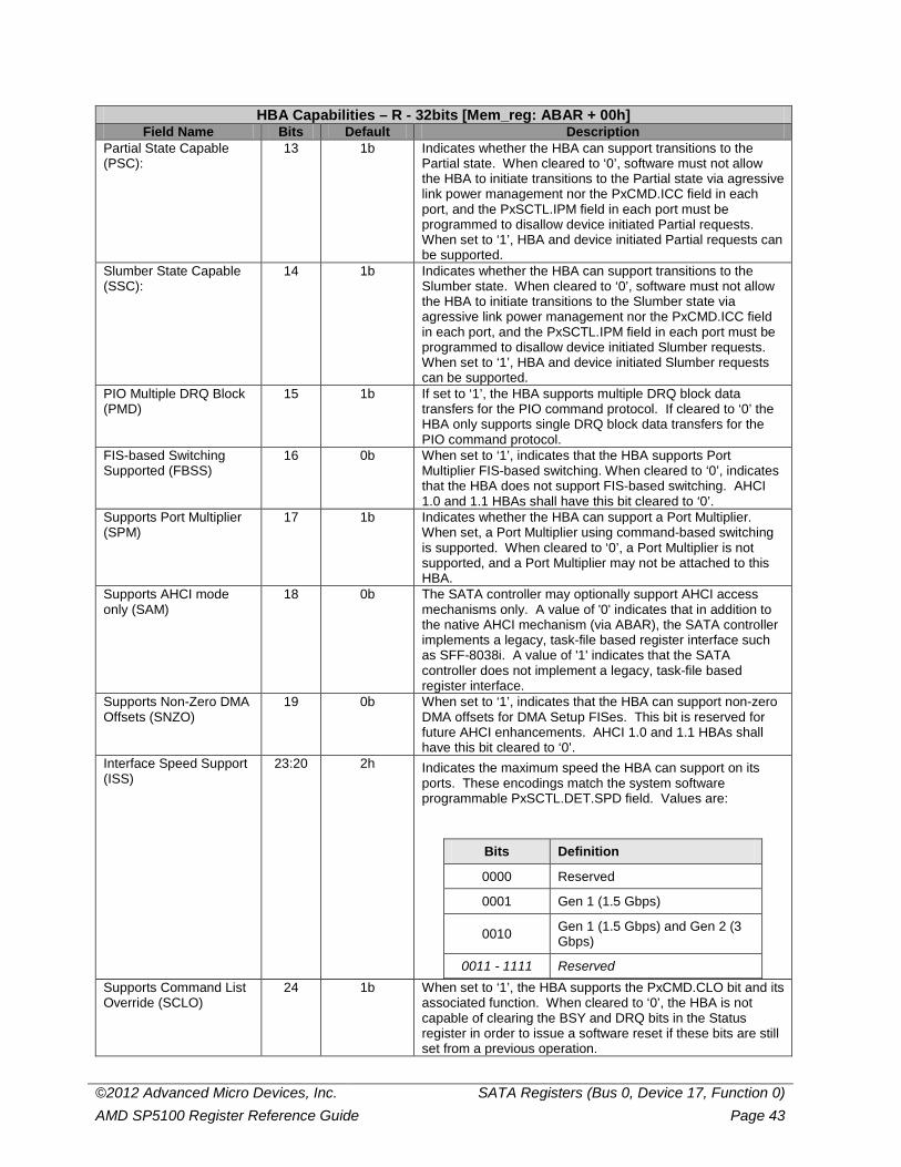
©2012 Advanced Micro Devices, Inc. SATA Registers (Bus 0, Device 17, Function 0) AMD SP5100 Register Reference Guide Page 43
HBA Capabilities – R - 32bits [Mem_reg: ABAR + 00h] Field Name Bits Default Description
Partial State Capable (PSC):
13 1b Indicates whether the HBA can support transitions to the Partial state. When cleared to ‘0’, software must not allow the HBA to initiate transitions to the Partial state via agressive link power management nor the PxCMD.ICC field in each port, and the PxSCTL.IPM field in each port must be programmed to disallow device initiated Partial requests. When set to ‘1’, HBA and device initiated Partial requests can be supported.
Slumber State Capable (SSC):
14 1b Indicates whether the HBA can support transitions to the Slumber state. When cleared to ‘0’, software must not allow the HBA to initiate transitions to the Slumber state via agressive link power management nor the PxCMD.ICC field in each port, and the PxSCTL.IPM field in each port must be programmed to disallow device initiated Slumber requests. When set to ‘1’, HBA and device initiated Slumber requests can be supported.
PIO Multiple DRQ Block (PMD)
15 1b If set to ‘1’, the HBA supports multiple DRQ block data transfers for the PIO command protocol. If cleared to ‘0’ the HBA only supports single DRQ block data transfers for the PIO command protocol.
FIS-based Switching Supported (FBSS)
16 0b When set to ‘1’, indicates that the HBA supports Port Multiplier FIS-based switching. When cleared to ‘0’, indicates that the HBA does not support FIS-based switching. AHCI 1.0 and 1.1 HBAs shall have this bit cleared to ‘0’.
Supports Port Multiplier (SPM)
17 1b Indicates whether the HBA can support a Port Multiplier. When set, a Port Multiplier using command-based switching is supported. When cleared to ‘0’, a Port Multiplier is not supported, and a Port Multiplier may not be attached to this HBA.
Supports AHCI mode only (SAM)
18 0b The SATA controller may optionally support AHCI access mechanisms only. A value of '0' indicates that in addition to the native AHCI mechanism (via ABAR), the SATA controller implements a legacy, task-file based register interface such as SFF-8038i. A value of '1' indicates that the SATA controller does not implement a legacy, task-file based register interface.
Supports Non-Zero DMA Offsets (SNZO)
19 0b When set to ‘1’, indicates that the HBA can support non-zero DMA offsets for DMA Setup FISes. This bit is reserved for future AHCI enhancements. AHCI 1.0 and 1.1 HBAs shall have this bit cleared to ‘0’.
Interface Speed Support (ISS)
23:20 2h Indicates the maximum speed the HBA can support on its ports. These encodings match the system software programmable PxSCTL.DET.SPD field. Values are:
Bits Definition
0000 Reserved
0001 Gen 1 (1.5 Gbps)
0010 Gen 1 (1.5 Gbps) and Gen 2 (3 Gbps)
0011 - 1111 Reserved
Supports Command List Override (SCLO)
24 1b When set to ‘1’, the HBA supports the PxCMD.CLO bit and its associated function. When cleared to ‘0’, the HBA is not capable of clearing the BSY and DRQ bits in the Status register in order to issue a software reset if these bits are still set from a previous operation.
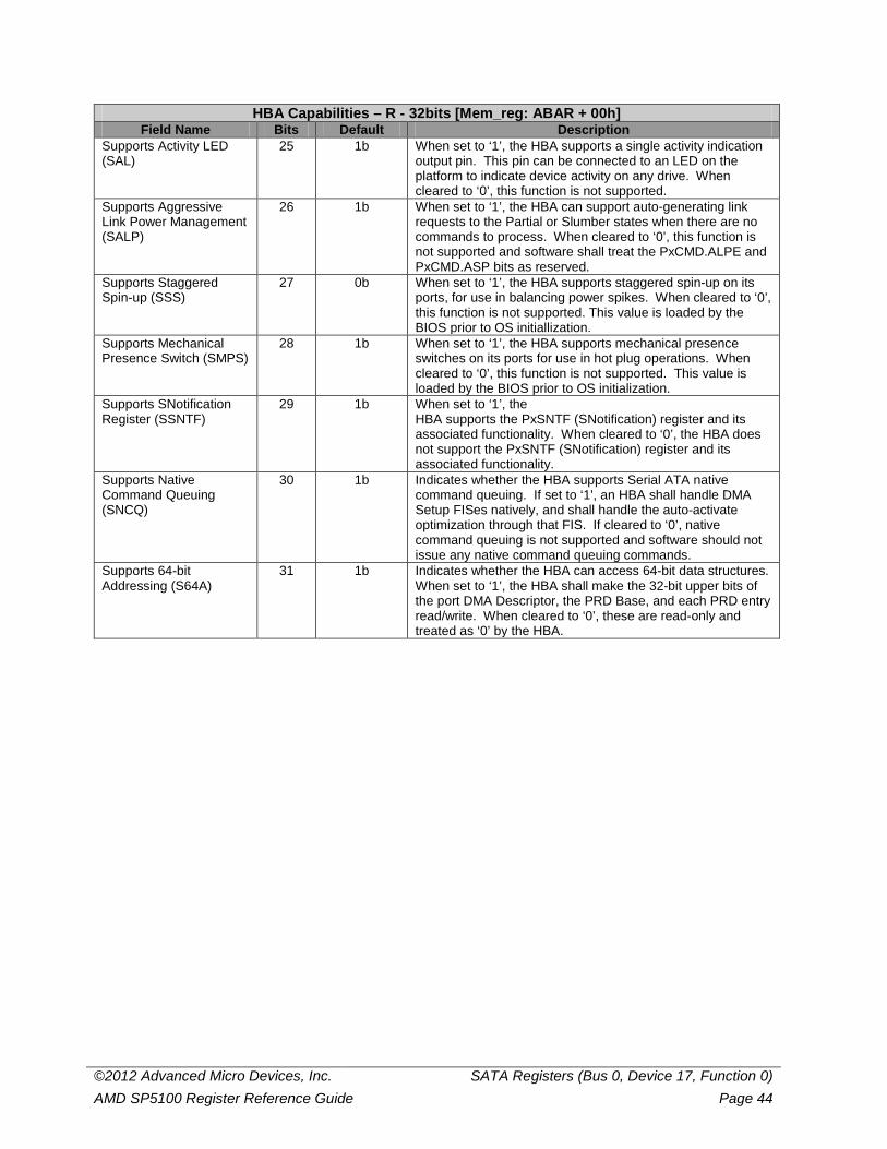
©2012 Advanced Micro Devices, Inc. SATA Registers (Bus 0, Device 17, Function 0) AMD SP5100 Register Reference Guide Page 44
HBA Capabilities – R - 32bits [Mem_reg: ABAR + 00h] Field Name Bits Default Description
Supports Activity LED (SAL)
25 1b When set to ‘1’, the HBA supports a single activity indication output pin. This pin can be connected to an LED on the platform to indicate device activity on any drive. When cleared to ‘0’, this function is not supported.
Supports Aggressive Link Power Management (SALP)
26 1b When set to ‘1’, the HBA can support auto-generating link requests to the Partial or Slumber states when there are no commands to process. When cleared to ‘0’, this function is not supported and software shall treat the PxCMD.ALPE and PxCMD.ASP bits as reserved.
Supports Staggered Spin-up (SSS)
27 0b When set to ‘1’, the HBA supports staggered spin-up on its ports, for use in balancing power spikes. When cleared to ‘0’, this function is not supported. This value is loaded by the BIOS prior to OS initiallization.
Supports Mechanical Presence Switch (SMPS)
28 1b When set to ‘1’, the HBA supports mechanical presence switches on its ports for use in hot plug operations. When cleared to ‘0’, this function is not supported. This value is loaded by the BIOS prior to OS initialization.
Supports SNotification Register (SSNTF)
29 1b When set to ‘1’, the HBA supports the PxSNTF (SNotification) register and its associated functionality. When cleared to ‘0’, the HBA does not support the PxSNTF (SNotification) register and its associated functionality.
Supports Native Command Queuing (SNCQ)
30 1b Indicates whether the HBA supports Serial ATA native command queuing. If set to ‘1’, an HBA shall handle DMA Setup FISes natively, and shall handle the auto-activate optimization through that FIS. If cleared to ‘0’, native command queuing is not supported and software should not issue any native command queuing commands.
Supports 64-bit Addressing (S64A)
31 1b Indicates whether the HBA can access 64-bit data structures. When set to ‘1’, the HBA shall make the 32-bit upper bits of the port DMA Descriptor, the PRD Base, and each PRD entry read/write. When cleared to ‘0’, these are read-only and treated as ‘0’ by the HBA.
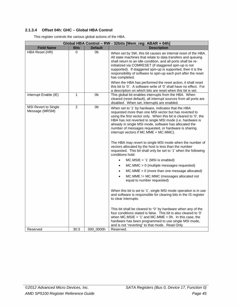
©2012 Advanced Micro Devices, Inc. SATA Registers (Bus 0, Device 17, Function 0) AMD SP5100 Register Reference Guide Page 45
2.1.3.4 Offset 04h: GHC – Global HBA Control This register controls the various global actions of the HBA.
Global HBA Control – RW - 32bits [Mem_reg: ABAR + 04h] Field Name Bits Default Description
HBA Reset (HR) 0 0b When set by SW, this bit causes an internal reset of the HBA. All state machines that relate to data transfers and queuing shall return to an idle condition, and all ports shall be re-initialized via COMRESET (if staggered spin-up is not supported). If staggered spin-up is supported, then it is the responsibility of software to spin-up each port after the reset has completed. When the HBA has performed the reset action, it shall reset this bit to ‘0’. A software write of ‘0’ shall have no effect. For a description on which bits are reset when this bit is set.
Interrupt Enable (IE) 1 0b This global bit enables interrupts from the HBA. When cleared (reset default), all interrupt sources from all ports are disabled. When set, interrupts are enabled.
MSI Revert to Single Message (MRSM)
2 0b When set to ‘1’ by hardware, indicates that the HBA requested more than one MSI vector but has reverted to using the first vector only. When this bit is cleared to ‘0’, the HBA has not reverted to single MSI mode (i.e. hardware is already in single MSI mode, software has allocated the number of messages requested, or hardware is sharing interrupt vectors if MC.MME < MC.MMC). The HBA may revert to single MSI mode when the number of vectors allocated by the host is less than the number requested. This bit shall only be set to ‘1’ when the following conditions hold:
• MC.MSIE = ‘1’ (MSI is enabled) • MC.MMC > 0 (multiple messages requested) • MC.MME > 0 (more than one message allocated) • MC.MME != MC.MMC (messages allocated not
equal to number requested) When this bit is set to ‘1’, single MSI mode operation is in use and software is responsible for clearing bits in the IS register to clear interrupts. This bit shall be cleared to ‘0’ by hardware when any of the four conditions stated is false. This bit is also cleared to ‘0’ when MC.MSIE = ‘1’ and MC.MME = 0h. In this case, the hardware has been programmed to use single MSI mode, and is not “reverting” to that mode. Read Only
Reserved 30:3 000_0000h Reserved.
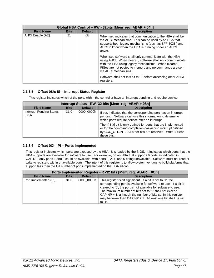
©2012 Advanced Micro Devices, Inc. SATA Registers (Bus 0, Device 17, Function 0) AMD SP5100 Register Reference Guide Page 46
Global HBA Control – RW - 32bits [Mem_reg: ABAR + 04h] Field Name Bits Default Description
AHCI Enable (AE) 31 0b When set, indicates that communication to the HBA shall be via AHCI mechanisms. This can be used by an HBA that supports both legacy mechanisms (such as SFF-8038i) and AHCI to know when the HBA is running under an AHCI driver.
When set, software shall only communicate with the HBA using AHCI. When cleared, software shall only communicate with the HBA using legacy mechanisms. When cleared FISes are not posted to memory and no commands are sent via AHCI mechanisms.
Software shall set this bit to ‘1’ before accessing other AHCI registers.
2.1.3.5 Offset 08h: IS – Interrupt Status Register This register indicates which of the ports within the controller have an interrupt pending and require service.
Interrupt Status - RW -32 bits [Mem_reg: ABAR + 08h] Field Name Bits Default Description
Interrupt Pending Status (IPS)
31:0 0000_0000h If set, indicates that the corresponding port has an interrupt pending. Software can use this information to determine which ports require service after an interrupt. The IPS[x] bit is only defined for ports that are implemented or for the command completion coalescing interrupt defined by CCC_CTL.INT. All other bits are reserved. Write 1 clear these bits.
2.1.3.6 Offset 0Ch: PI – Ports Implemented This register indicates which ports are exposed by the HBA. It is loaded by the BIOS. It indicates which ports that the HBA supports are available for software to use. For example, on an HBA that supports 6 ports as indicated in CAP.NP, only ports 1 and 3 could be available, with ports 0, 2, 4, and 5 being unavailable. Software must not read or write to registers within unavailable ports. The intent of this register is to allow system vendors to build platforms that support less than the full number of ports implemented on the HBA silicon.
Ports Implemented Register - R -32 bits [Mem_reg: ABAR + 0Ch] Field Name Bits Default Description
Port Implemented (PI) 31:0 0000_000Fh This register is bit significant. If a bit is set to ‘1’, the corresponding port is available for software to use. If a bit is cleared to ‘0’, the port is not available for software to use. The maximum number of bits set to ‘1’ shall not exceed CAP.NP + 1, although the number of bits set in this register may be fewer than CAP.NP + 1. At least one bit shall be set to ‘1’.
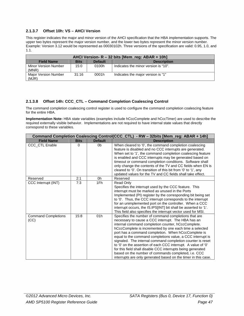
©2012 Advanced Micro Devices, Inc. SATA Registers (Bus 0, Device 17, Function 0) AMD SP5100 Register Reference Guide Page 47
2.1.3.7 Offset 10h: VS – AHCI Version This register indicates the major and minor version of the AHCI specification that the HBA implementation supports. The upper two bytes represent the major version number, and the lower two bytes represent the minor version number. Example: Version 3.12 would be represented as 00030102h. Three versions of the specification are valid: 0.95, 1.0, and 1.1.
AHCI Version- R – 32 bits [Mem_reg: ABAR + 10h] Field Name Bits Default Description
Minor Version Number (MNR)
15:0 0100h Indicates the minor version is “10”.
Major Version Number (MJR)
31:16 0001h Indicates the major version is “1”
2.1.3.8 Offset 14h: CCC_CTL – Command Completion Coalescing Control The command completion coalescing control register is used to configure the command completion coalescing feature for the entire HBA.
Implementation Note: HBA state variables (examples include hCccComplete and hCccTimer) are used to describe the required externally visible behavior. Implementations are not required to have internal state values that directly correspond to these variables.
Command Completion Coalescing Control(CCC_CTL) - RW – 32bits [Mem_reg: ABAR + 14h] Field Name Bits Default Description
CCC_CTL Enable 0 0b When cleared to ‘0’, the command completion coalescing feature is disabled and no CCC interrupts are generated. When set to ‘1’, the command completion coalescing feature is enabled and CCC interrupts may be generated based on timeout or command completion conditions. Software shall only change the contents of the TV and CC fields when EN is cleared to ‘0’. On transition of this bit from ‘0’ to ‘1’, any updated values for the TV and CC fields shall take effect.
Reserved 2:1 0h Reserved CCC Interrupt (INT) 7:3 1Fh Read Only
Specifies the interrupt used by the CCC feature. This interrupt must be marked as unused in the Ports Implemented (PI) register by the corresponding bit being set to ‘0’. Thus, the CCC interrupt corresponds to the interrupt for an unimplemented port on the controller. When a CCC interrupt occurs, the IS.IPS[INT] bit shall be asserted to ‘1’. This field also specifies the interrupt vector used for MSI.
Command Completions (CC)
15:8 01h Specifies the number of command completions that are necessary to cause a CCC interrupt. The HBA has an internal command completion counter, hCccComplete. hCccComplete is incremented by one each time a selected port has a command completion. When hCccComplete is equal to the command completions value, a CCC interrupt is signaled. The internal command completion counter is reset to ‘0’ on the assertion of each CCC interrupt. A value of ‘0’ for this field shall disable CCC interrupts being generated based on the number of commands completed, i.e. CCC interrupts are only generated based on the timer in this case.
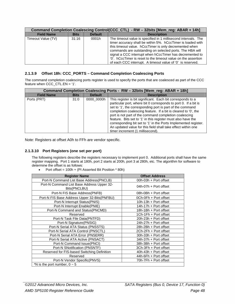
©2012 Advanced Micro Devices, Inc. SATA Registers (Bus 0, Device 17, Function 0) AMD SP5100 Register Reference Guide Page 48
Command Completion Coalescing Control(CCC_CTL) - RW – 32bits [Mem_reg: ABAR + 14h] Field Name Bits Default Description
Timeout Value (TV) 31:16 0001h The timeout value is specified in 1 millisecond intervals. The timer accuracy shall be within 5%. hCccTimer is loaded with this timeout value. hCccTimer is only decremented when commands are outstanding on selected ports. The HBA will signal a CCC interrupt when hCccTimer has decremented to ‘0’. hCccTimer is reset to the timeout value on the assertion of each CCC interrupt. A timeout value of ‘0’ is reserved.
2.1.3.9 Offset 18h: CCC_PORTS – Command Completion Coalescing Ports The command completion coalescing ports register is used to specify the ports that are coalesced as part of the CCC feature when CCC_CTL.EN = ‘1’.
Command Completion Coalescing Ports - RW – 32bits [Mem_reg: ABAR + 18h] Field Name Bits Default Description
Ports (PRT) 31:0 0000_0000h This register is bit significant. Each bit corresponds to a particular port, where bit 0 corresponds to port 0. If a bit is set to ‘1’, the corresponding port is part of the command completion coalescing feature. If a bit is cleared to ‘0’, the port is not part of the command completion coalescing feature. Bits set to ‘1’ in this register must also have the corresponding bit set to ‘1’ in the Ports Implemented register. An updated value for this field shall take effect within one timer increment (1 millisecond).
Note: Registers at offset A0h to FFh are vendor specific.
2.1.3.10 Port Registers (one set per port) The following registers describe the registers necessary to implement port 0. Additional ports shall have the same register mapping. Port 1 starts at 180h, port 2 starts at 200h, port 3 at 280h, etc. The algorithm for software to determine the offset is as follows:
• Port offset = 100h + (PI Asserted Bit Position * 80h)
Register Name Offset Address Port-N Command List Base Address(PNCLB) 00h-03h + Port offset
Port-N Command List Base Address Upper 32-Bits(PNCLBU) 04h-07h + Port offset
Port-N FIS Base Address(PNFB) 08h-0Bh + Port offset Port-N FIS Base Address Upper 32-Bits(PNFBU) 0Ch-0Fh + Port offset
Port-N Interrupt Status(PNIS) 10h-13h + Port offset Port-N Interrupt Enable(PNIE) 14h-17h + Port offset
Port-N Command and Status(PNCMD) 18h-1Bh + Port offset Reserved 1Ch-1Fh + Port offset
Port-N Task File Data(PNTFD) 20h-23h + Port offset Port-N Signature(PNSIG) 24h-27h + Port offset
Port-N Serial ATA Status (PNSSTS) 28h-2Bh + Port offset Port-N Serial ATA Control (PNSCTL) 2Ch-2Fh + Port offset Port-N Serial ATA Error (PNSERR) 30h-33h + Port offset Port-N Serial ATA Active (PNSACT) 34h-37h + Port offset
Port-N Command Issue(PNCI) 38h-3Bh + Port offset Port-N SNotification (PNSNTF) 3Ch-3Fh + Port offset
Reserved for FIS-based Switching Definition 40h-43h + Port offset Reserved 44h-6Fh + Port offset
Port-N Vendor Specific(PNVS) 70h-7Fh + Port offset *N is the port number, 0 ~ 5
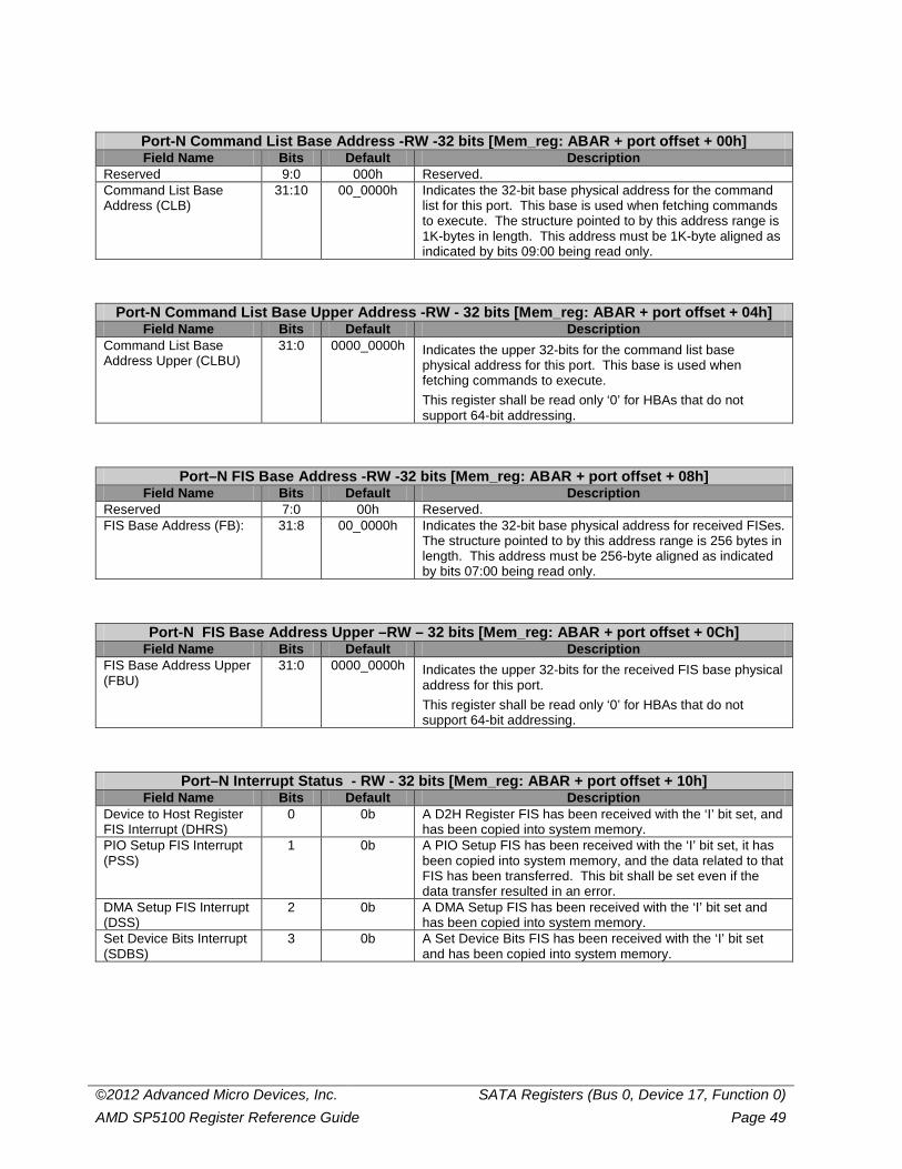
©2012 Advanced Micro Devices, Inc. SATA Registers (Bus 0, Device 17, Function 0) AMD SP5100 Register Reference Guide Page 49
Port-N Command List Base Address -RW -32 bits [Mem_reg: ABAR + port offset + 00h] Field Name Bits Default Description
Reserved 9:0 000h Reserved. Command List Base Address (CLB)
31:10 00_0000h Indicates the 32-bit base physical address for the command list for this port. This base is used when fetching commands to execute. The structure pointed to by this address range is 1K-bytes in length. This address must be 1K-byte aligned as indicated by bits 09:00 being read only.
Port-N Command List Base Upper Address -RW - 32 bits [Mem_reg: ABAR + port offset + 04h] Field Name Bits Default Description
Command List Base Address Upper (CLBU)
31:0 0000_0000h Indicates the upper 32-bits for the command list base physical address for this port. This base is used when fetching commands to execute. This register shall be read only ‘0’ for HBAs that do not support 64-bit addressing.
Port–N FIS Base Address -RW -32 bits [Mem_reg: ABAR + port offset + 08h] Field Name Bits Default Description
Reserved 7:0 00h Reserved. FIS Base Address (FB): 31:8 00_0000h Indicates the 32-bit base physical address for received FISes.
The structure pointed to by this address range is 256 bytes in length. This address must be 256-byte aligned as indicated by bits 07:00 being read only.
Port-N FIS Base Address Upper –RW – 32 bits [Mem_reg: ABAR + port offset + 0Ch] Field Name Bits Default Description
FIS Base Address Upper (FBU)
31:0 0000_0000h Indicates the upper 32-bits for the received FIS base physical address for this port. This register shall be read only ‘0’ for HBAs that do not support 64-bit addressing.
Port–N Interrupt Status - RW - 32 bits [Mem_reg: ABAR + port offset + 10h] Field Name Bits Default Description
Device to Host Register FIS Interrupt (DHRS)
0 0b A D2H Register FIS has been received with the ‘I’ bit set, and has been copied into system memory.
PIO Setup FIS Interrupt (PSS)
1 0b A PIO Setup FIS has been received with the ‘I’ bit set, it has been copied into system memory, and the data related to that FIS has been transferred. This bit shall be set even if the data transfer resulted in an error.
DMA Setup FIS Interrupt (DSS)
2 0b A DMA Setup FIS has been received with the ‘I’ bit set and has been copied into system memory.
Set Device Bits Interrupt (SDBS)
3 0b A Set Device Bits FIS has been received with the ‘I’ bit set and has been copied into system memory.
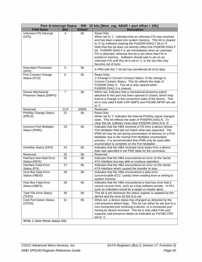
©2012 Advanced Micro Devices, Inc. SATA Registers (Bus 0, Device 17, Function 0) AMD SP5100 Register Reference Guide Page 50
Port–N Interrupt Status - RW - 32 bits [Mem_reg: ABAR + port offset + 10h] Field Name Bits Default Description
Unknown FIS Interrupt (UFS)
4 0b Read Only When set to ‘1’, indicates that an unknown FIS was received and has been copied into system memory. This bit is cleared to ‘0’ by software clearing the PxSERR.DIAG.F bit to ‘0’. Note that this bit does not directly reflect the PxSERR.DIAG.F bit. PxSERR.DIAG.F is set immediately when an unknown FIS is detected, whereas this bit is set when that FIS is posted to memory. Software should wait to act on an unknown FIS until this bit is set to ‘1’ or the two bits may become out of sync.
Descriptor Processed (DPS)
5 0b A PRD with the ‘I’ bit set has transferred all of its data.
Port Connect Change Status (PCS)
6 0b Read Onby 1=Change in Current Connect Status. 0=No change in Current Connect Status. This bit reflects the state of PxSERR.DIAG.X. This bit is only cleared when PxSERR.DIAG.X is cleared.
Device Mechanical Presence Status (DMPS)
7 0b When set, indicates that a mechanical presence switch attached to this port has been opened or closed, which may lead to a change in the connection state of the device. This bit is only valid if both CAP.SMPS and P0CMD.MPSP are set to ‘1’.
Reserved 21:8 0000h Reserved PhyRdy Change Status (PRCS)
22 0b Read Only When set to ‘1’ indicates the internal PhyRdy signal changed state. This bit reflects the state of P0SERR.DIAG.N. To clear this bit, software must clear P0SERR.DIAG.N to ‘0’.
Incorrect Port Multiplier Status (IPMS):
23 0b Indicates that the HBA received a FIS from a device whose Port Multiplier field did not match what was expected. The IPMS bit may be set during enumeration of devices on a Port Multiplier due to the normal Port Multiplier enumeration process. It is recommended that IPMS only be used after enumeration is complete on the Port Multiplier.
Overflow Status (OFS) 24 0b Indicates that the HBA received more bytes from a device than was specified in the PRD table for the command.
Reserved 25 0b Reserved Interface Non-fatal Error Status (INFS)
26 0b Indicates that the HBA encountered an error on the Serial ATA interface but was able to continue operation.
Interface Fatal Error Status (IFS)
27 0b Indicates that the HBA encountered an error on the Serial ATA interface which caused the transfer to stop.
Host Bus Data Error Status (HBDS)
28 0b Indicates that the HBA encountered a data error (uncorrectable ECC / parity) when reading from or writing to system memory.
Host Bus Fatal Error Status (HBFS)
29 0b Indicates that the HBA encountered a host bus error that it cannot recover from, such as a bad software pointer. In PCI, such an indication would be a target or master abort.
Task File Error Status (TFES):
30 0b This bit is set whenever the status register is updated by the device and the error bit (bit 0) is set.
Cold Port Detect Status (CPDS)
31 0b When set, a device status has changed as detected by the cold presence detect logic. This bit can either be set due to a non-connected port receiving a device, or a connected port having its device removed. This bit is only valid if the port supports cold presence detect as indicated by PxCMD.CPD set to ‘1’.
Write 1 clear these status bits
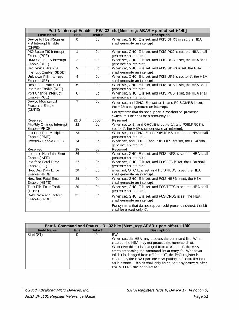
©2012 Advanced Micro Devices, Inc. SATA Registers (Bus 0, Device 17, Function 0) AMD SP5100 Register Reference Guide Page 51
Port-N Interrupt Enable - RW -32 bits [Mem_reg: ABAR + port offset + 14h] Field Name Bits Default Description
Device to Host Register FIS Interrupt Enable (DHRE)
0 0b When set, GHC.IE is set, and P0IS.DHRS is set, the HBA shall generate an interrupt.
PIO Setup FIS Interrupt Enable (PSE)
1 0b When set, GHC.IE is set, and P0IS.PSS is set, the HBA shall generate an interrupt.
DMA Setup FIS Interrupt Enable (DSE)
2 0b When set, GHC.IE is set, and P0IS.DSS is set, the HBA shall generate an interrupt.
Set Device Bits FIS Interrupt Enable (SDBE)
3 0b When set, GHC.IE is set, and P0IS.SDBS is set, the HBA shall generate an interrupt.
Unknown FIS Interrupt Enable (UFE)
4 0b When set, GHC.IE is set, and P0IS.UFS is set to ‘1’, the HBA shall generate an interrupt.
Descriptor Processed Interrupt Enable (DPE)
5 0b When set, GHC.IE is set, and P0IS.DPS is set, the HBA shall generate an interrupt.
Port Change Interrupt Enable (PCE)
6 0b When set, GHC.IE is set, and P0IS.PCS is set, the HBA shall generate an interrupt.
Device Mechanical Presence Enable (DMPE)
7 0b When set, and GHC.IE is set to ‘1’, and P0IS.DMPS is set, the HBA shall generate an interrupt. For systems that do not support a mechanical presence switch, this bit shall be a read-only ‘0’.
Reserved 21:8 0000h Reserved PhyRdy Change Interrupt Enable (PRCE)
22 0b When set to ‘1’, and GHC.IE is set to ‘1’, and P0IS.PRCS is set to ‘1’, the HBA shall generate an interrupt.
Incorrect Port Multiplier Enable (IPME)
23 0b When set, and GHC.IE and P0IS.IPMS are set, the HBA shall generate an interupt.
Overflow Enable (OFE) 24 0b When set, and GHC.IE and P0IS.OFS are set, the HBA shall generate an interupt.
Reserved 25 0b Reserved Interface Non-fatal Error Enable (INFE)
26 0b When set, GHC.IE is set, and P0IS.INFS is set, the HBA shall generate an interrupt.
Interface Fatal Error Enable (IFE)
27 0b When set, GHC.IE is set, and P0IS.IFS is set, the HBA shall generate an interrupt..
Host Bus Data Error Enable (HBDE)
28 0b when set, GHC.IE is set, and P0IS.HBDS is set, the HBA shall generate an interrupt..
Host Bus Fatal Error Enable (HBFE)
29 0b When set, GHC.IE is set, and P0IS.HBFS is set, the HBA shall generate an interrupt.
Task File Error Enable (TFEE)
30 0b When set, GHC.IE is set, and P0S.TFES is set, the HBA shall generate an interrupt.
Cold Presence Detect Enable (CPDE)
31 0b When set, GHC.IE is set, and P0S.CPDS is set, the HBA shall generate an interrupt. For systems that do not support cold presence detect, this bit shall be a read-only ‘0’.
Port-N Command and Status - R - 32 bits [Mem_reg: ABAR + port offset + 18h] Field Name Bits Default Description
Start (ST) 0 0b RW When set, the HBA may process the command list. When cleared, the HBA may not process the command list. Whenever this bit is changed from a ‘0’ to a ‘1’, the HBA starts processing the command list at entry ‘0’. Whenever this bit is changed from a ‘1’ to a ‘0’, the PxCI register is cleared by the HBA upon the HBA putting the controller into an idle state. This bit shall only be set to ‘1’ by software after PxCMD.FRE has been set to ‘1’.
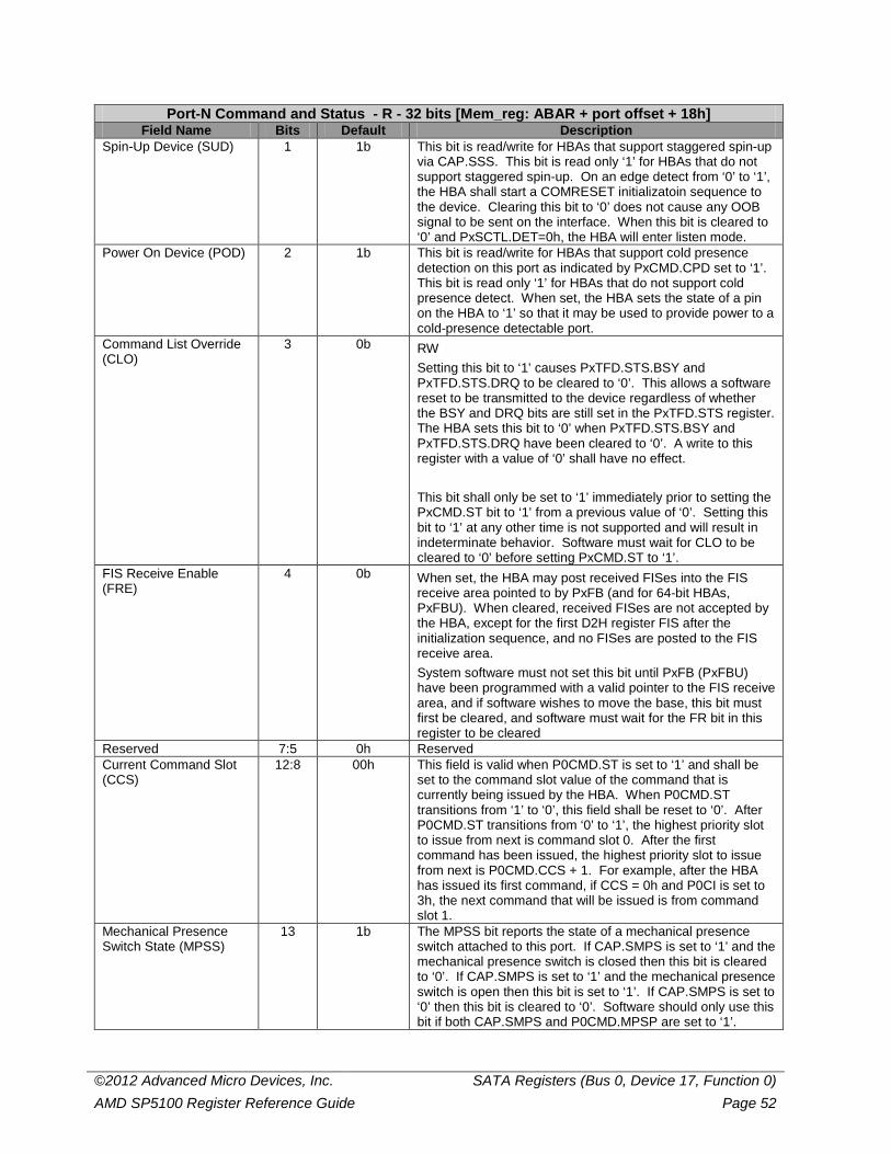
©2012 Advanced Micro Devices, Inc. SATA Registers (Bus 0, Device 17, Function 0) AMD SP5100 Register Reference Guide Page 52
Port-N Command and Status - R - 32 bits [Mem_reg: ABAR + port offset + 18h] Field Name Bits Default Description
Spin-Up Device (SUD) 1 1b This bit is read/write for HBAs that support staggered spin-up via CAP.SSS. This bit is read only ‘1’ for HBAs that do not support staggered spin-up. On an edge detect from ‘0’ to ‘1’, the HBA shall start a COMRESET initializatoin sequence to the device. Clearing this bit to ‘0’ does not cause any OOB signal to be sent on the interface. When this bit is cleared to ‘0’ and PxSCTL.DET=0h, the HBA will enter listen mode.
Power On Device (POD) 2 1b This bit is read/write for HBAs that support cold presence detection on this port as indicated by PxCMD.CPD set to ‘1’. This bit is read only ‘1’ for HBAs that do not support cold presence detect. When set, the HBA sets the state of a pin on the HBA to ‘1’ so that it may be used to provide power to a cold-presence detectable port.
Command List Override (CLO)
3 0b RW Setting this bit to ‘1’ causes PxTFD.STS.BSY and PxTFD.STS.DRQ to be cleared to ‘0’. This allows a software reset to be transmitted to the device regardless of whether the BSY and DRQ bits are still set in the PxTFD.STS register. The HBA sets this bit to ‘0’ when PxTFD.STS.BSY and PxTFD.STS.DRQ have been cleared to ‘0’. A write to this register with a value of ‘0’ shall have no effect. This bit shall only be set to ‘1’ immediately prior to setting the PxCMD.ST bit to ‘1’ from a previous value of ‘0’. Setting this bit to ‘1’ at any other time is not supported and will result in indeterminate behavior. Software must wait for CLO to be cleared to ‘0’ before setting PxCMD.ST to ‘1’.
FIS Receive Enable (FRE)
4 0b When set, the HBA may post received FISes into the FIS receive area pointed to by PxFB (and for 64-bit HBAs, PxFBU). When cleared, received FISes are not accepted by the HBA, except for the first D2H register FIS after the initialization sequence, and no FISes are posted to the FIS receive area. System software must not set this bit until PxFB (PxFBU) have been programmed with a valid pointer to the FIS receive area, and if software wishes to move the base, this bit must first be cleared, and software must wait for the FR bit in this register to be cleared
Reserved 7:5 0h Reserved Current Command Slot (CCS)
12:8 00h This field is valid when P0CMD.ST is set to ‘1’ and shall be set to the command slot value of the command that is currently being issued by the HBA. When P0CMD.ST transitions from ‘1’ to ‘0’, this field shall be reset to ‘0’. After P0CMD.ST transitions from ‘0’ to ‘1’, the highest priority slot to issue from next is command slot 0. After the first command has been issued, the highest priority slot to issue from next is P0CMD.CCS + 1. For example, after the HBA has issued its first command, if CCS = 0h and P0CI is set to 3h, the next command that will be issued is from command slot 1.
Mechanical Presence Switch State (MPSS)
13 1b The MPSS bit reports the state of a mechanical presence switch attached to this port. If CAP.SMPS is set to ‘1’ and the mechanical presence switch is closed then this bit is cleared to ‘0’. If CAP.SMPS is set to ‘1’ and the mechanical presence switch is open then this bit is set to ‘1’. If CAP.SMPS is set to ‘0’ then this bit is cleared to ‘0’. Software should only use this bit if both CAP.SMPS and P0CMD.MPSP are set to ‘1’.
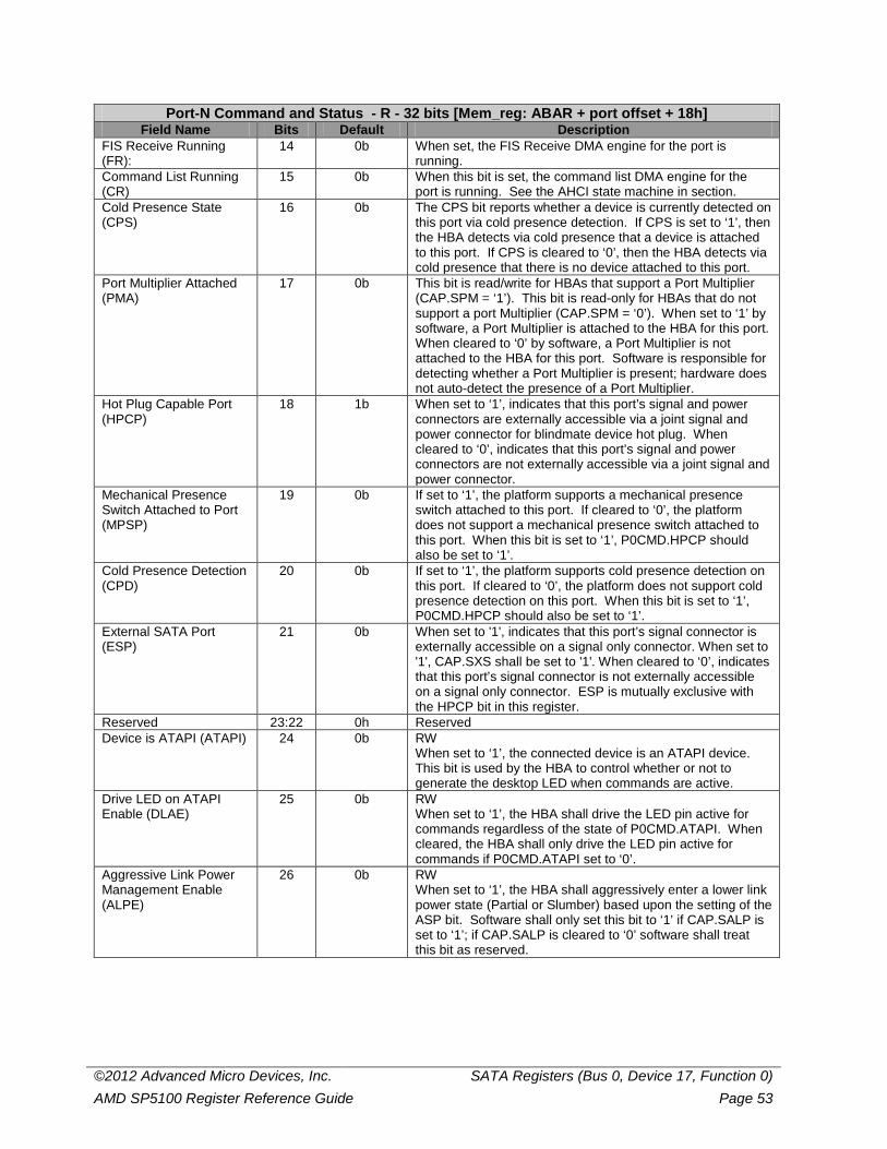
©2012 Advanced Micro Devices, Inc. SATA Registers (Bus 0, Device 17, Function 0) AMD SP5100 Register Reference Guide Page 53
Port-N Command and Status - R - 32 bits [Mem_reg: ABAR + port offset + 18h] Field Name Bits Default Description
FIS Receive Running (FR):
14 0b When set, the FIS Receive DMA engine for the port is running.
Command List Running (CR)
15 0b When this bit is set, the command list DMA engine for the port is running. See the AHCI state machine in section.
Cold Presence State (CPS)
16 0b The CPS bit reports whether a device is currently detected on this port via cold presence detection. If CPS is set to ‘1’, then the HBA detects via cold presence that a device is attached to this port. If CPS is cleared to ‘0’, then the HBA detects via cold presence that there is no device attached to this port.
Port Multiplier Attached (PMA)
17 0b This bit is read/write for HBAs that support a Port Multiplier (CAP.SPM = ‘1’). This bit is read-only for HBAs that do not support a port Multiplier (CAP.SPM = ‘0’). When set to ‘1’ by software, a Port Multiplier is attached to the HBA for this port. When cleared to ‘0’ by software, a Port Multiplier is not attached to the HBA for this port. Software is responsible for detecting whether a Port Multiplier is present; hardware does not auto-detect the presence of a Port Multiplier.
Hot Plug Capable Port (HPCP)
18 1b When set to ‘1’, indicates that this port’s signal and power connectors are externally accessible via a joint signal and power connector for blindmate device hot plug. When cleared to ‘0’, indicates that this port’s signal and power connectors are not externally accessible via a joint signal and power connector.
Mechanical Presence Switch Attached to Port (MPSP)
19 0b If set to ‘1’, the platform supports a mechanical presence switch attached to this port. If cleared to ‘0’, the platform does not support a mechanical presence switch attached to this port. When this bit is set to ‘1’, P0CMD.HPCP should also be set to ‘1’.
Cold Presence Detection (CPD)
20 0b If set to ‘1’, the platform supports cold presence detection on this port. If cleared to ‘0’, the platform does not support cold presence detection on this port. When this bit is set to ‘1’, P0CMD.HPCP should also be set to ‘1’.
External SATA Port (ESP)
21 0b When set to '1', indicates that this port’s signal connector is externally accessible on a signal only connector. When set to '1', CAP.SXS shall be set to '1'. When cleared to ‘0’, indicates that this port’s signal connector is not externally accessible on a signal only connector. ESP is mutually exclusive with the HPCP bit in this register.
Reserved 23:22 0h Reserved Device is ATAPI (ATAPI) 24 0b RW
When set to ‘1’, the connected device is an ATAPI device. This bit is used by the HBA to control whether or not to generate the desktop LED when commands are active.
Drive LED on ATAPI Enable (DLAE)
25 0b RW When set to ‘1’, the HBA shall drive the LED pin active for commands regardless of the state of P0CMD.ATAPI. When cleared, the HBA shall only drive the LED pin active for commands if P0CMD.ATAPI set to ‘0’.
Aggressive Link Power Management Enable (ALPE)
26 0b RW When set to ‘1’, the HBA shall aggressively enter a lower link power state (Partial or Slumber) based upon the setting of the ASP bit. Software shall only set this bit to ‘1’ if CAP.SALP is set to ‘1’; if CAP.SALP is cleared to ‘0’ software shall treat this bit as reserved.
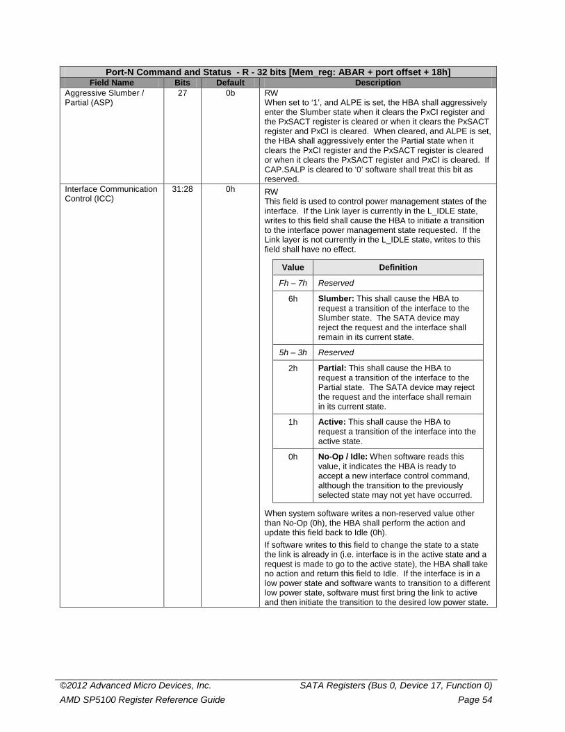
©2012 Advanced Micro Devices, Inc. SATA Registers (Bus 0, Device 17, Function 0) AMD SP5100 Register Reference Guide Page 54
Port-N Command and Status - R - 32 bits [Mem_reg: ABAR + port offset + 18h] Field Name Bits Default Description
Aggressive Slumber / Partial (ASP)
27 0b RW When set to ‘1’, and ALPE is set, the HBA shall aggressively enter the Slumber state when it clears the PxCI register and the PxSACT register is cleared or when it clears the PxSACT register and PxCI is cleared. When cleared, and ALPE is set, the HBA shall aggressively enter the Partial state when it clears the PxCI register and the PxSACT register is cleared or when it clears the PxSACT register and PxCI is cleared. If CAP.SALP is cleared to ‘0’ software shall treat this bit as reserved.
Interface Communication Control (ICC)
31:28 0h RW This field is used to control power management states of the interface. If the Link layer is currently in the L_IDLE state, writes to this field shall cause the HBA to initiate a transition to the interface power management state requested. If the Link layer is not currently in the L_IDLE state, writes to this field shall have no effect.
Value Definition
Fh – 7h Reserved
6h Slumber: This shall cause the HBA to request a transition of the interface to the Slumber state. The SATA device may reject the request and the interface shall remain in its current state.
5h – 3h Reserved
2h Partial: This shall cause the HBA to request a transition of the interface to the Partial state. The SATA device may reject the request and the interface shall remain in its current state.
1h Active: This shall cause the HBA to request a transition of the interface into the active state.
0h No-Op / Idle: When software reads this value, it indicates the HBA is ready to accept a new interface control command, although the transition to the previously selected state may not yet have occurred.
When system software writes a non-reserved value other than No-Op (0h), the HBA shall perform the action and update this field back to Idle (0h). If software writes to this field to change the state to a state the link is already in (i.e. interface is in the active state and a request is made to go to the active state), the HBA shall take no action and return this field to Idle. If the interface is in a low power state and software wants to transition to a different low power state, software must first bring the link to active and then initiate the transition to the desired low power state.
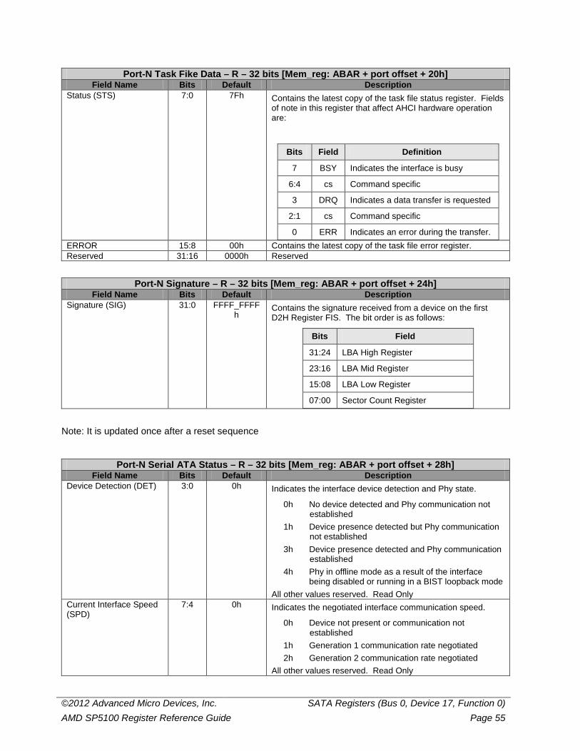
©2012 Advanced Micro Devices, Inc. SATA Registers (Bus 0, Device 17, Function 0) AMD SP5100 Register Reference Guide Page 55
Port-N Task Fike Data – R – 32 bits [Mem_reg: ABAR + port offset + 20h] Field Name Bits Default Description
Status (STS) 7:0 7Fh Contains the latest copy of the task file status register. Fields of note in this register that affect AHCI hardware operation are:
Bits Field Definition
7 BSY Indicates the interface is busy
6:4 cs Command specific
3 DRQ Indicates a data transfer is requested
2:1 cs Command specific
0 ERR Indicates an error during the transfer.
ERROR 15:8 00h Contains the latest copy of the task file error register. Reserved 31:16 0000h Reserved
Port-N Signature – R – 32 bits [Mem_reg: ABAR + port offset + 24h] Field Name Bits Default Description
Signature (SIG) 31:0 FFFF_FFFFh
Contains the signature received from a device on the first D2H Register FIS. The bit order is as follows:
Bits Field
31:24 LBA High Register
23:16 LBA Mid Register
15:08 LBA Low Register
07:00 Sector Count Register
Note: It is updated once after a reset sequence
Port-N Serial ATA Status – R – 32 bits [Mem_reg: ABAR + port offset + 28h] Field Name Bits Default Description
Device Detection (DET) 3:0 0h Indicates the interface device detection and Phy state.
0h No device detected and Phy communication not established 1h Device presence detected but Phy communication not established 3h Device presence detected and Phy communication established 4h Phy in offline mode as a result of the interface
being disabled or running in a BIST loopback mode All other values reserved. Read Only
Current Interface Speed (SPD)
7:4 0h Indicates the negotiated interface communication speed.
0h Device not present or communication not established 1h Generation 1 communication rate negotiated 2h Generation 2 communication rate negotiated All other values reserved. Read Only
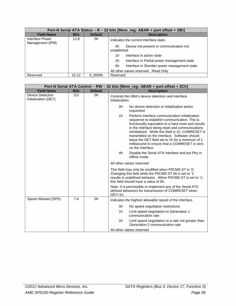
©2012 Advanced Micro Devices, Inc. SATA Registers (Bus 0, Device 17, Function 0) AMD SP5100 Register Reference Guide Page 56
Port-N Serial ATA Status – R – 32 bits [Mem_reg: ABAR + port offset + 28h] Field Name Bits Default Description
Interface Power Management (IPM)
11:8 0h Indicates the current interface state:
0h Device not present or communication not established 1h Interface in active state 2h Interface in Partial power management state 6h Interface in Slumber power management state All other values reserved. Read Only
Reserved 31:12 0_0000h Reserved
Port-N Serial ATA Control – RW – 32 bits [Mem_reg: ABAR + port offset + 2Ch] Field Name Bits Default Description
Device Detection Initialization (DET)
3:0 0h Controls the HBA’s device detection and interface initialization.
0h No device detection or initialization action requested
1h Perform interface communication initialization sequence to establish communication. This is functionally equivalent to a hard reset and results in the interface being reset and communications reinitialized. While this field is 1h, COMRESET is transmitted on the interface. Software should leave the DET field set to 1h for a minimum of 1 millisecond to ensure that a COMRESET is sent on the interface.
4h Disable the Serial ATA interface and put Phy in offline mode.
All other values reserved
This field may only be modified when P0CMD.ST is ‘0’. Changing this field while the P0CMD.ST bit is set to ‘1’ results in undefined behavior. When P0CMD.ST is set to ‘1’, this field should have a value of 0h. Note: It is permissible to implement any of the Serial ATA defined behaviors for transmission of COMRESET when DET=1h.
Speed Allowed (SPD) 7:4 0h Indicates the highest allowable speed of the interface.
0h No speed negotiation restrictions 1h Limit speed negotiation to Generation 1 communication rate 2h Limit speed negotiation to a rate not greater than
Generation 2 communication rate All other values reserved
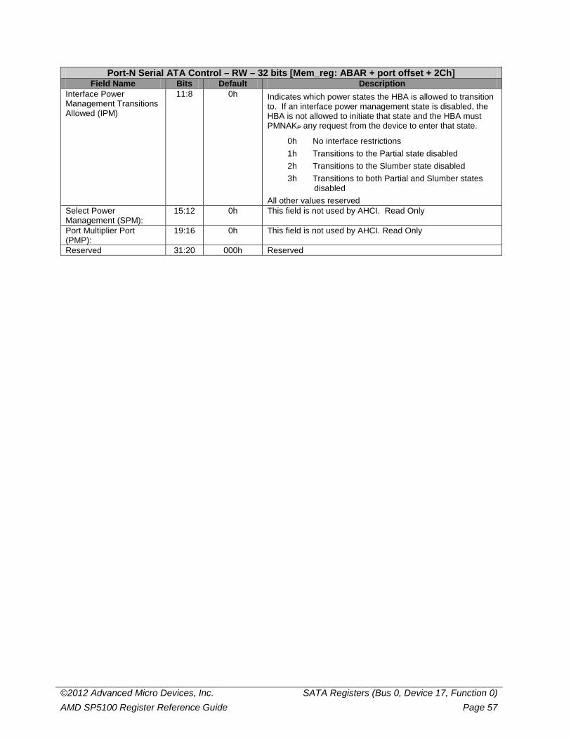
©2012 Advanced Micro Devices, Inc. SATA Registers (Bus 0, Device 17, Function 0) AMD SP5100 Register Reference Guide Page 57
Port-N Serial ATA Control – RW – 32 bits [Mem_reg: ABAR + port offset + 2Ch] Field Name Bits Default Description
Interface Power Management Transitions Allowed (IPM)
11:8 0h Indicates which power states the HBA is allowed to transition to. If an interface power management state is disabled, the HBA is not allowed to initiate that state and the HBA must PMNAKP any request from the device to enter that state.
0h No interface restrictions 1h Transitions to the Partial state disabled 2h Transitions to the Slumber state disabled 3h Transitions to both Partial and Slumber states disabled All other values reserved
Select Power Management (SPM):
15:12 0h This field is not used by AHCI. Read Only
Port Multiplier Port (PMP):
19:16 0h This field is not used by AHCI. Read Only
Reserved 31:20 000h Reserved
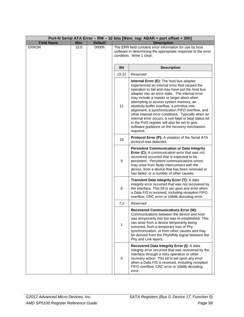
©2012 Advanced Micro Devices, Inc. SATA Registers (Bus 0, Device 17, Function 0) AMD SP5100 Register Reference Guide Page 58
Port-N Serial ATA Error – RW – 32 bits [Mem_reg: ABAR + port offset + 30h] Field Name Bits Default Description
ERROR 15:0 0000h The ERR field contains error information for use by host software in determining the appropriate response to the error condition. Write 1 clear.
Bit Description
15:12 Reserved
11
Internal Error (E): The host bus adapter experienced an internal error that caused the operation to fail and may have put the host bus adapter into an error state. The internal error may include a master or target abort when attempting to access system memory, an elasticity buffer overflow, a primitive mis-alignment, a synchronization FIFO overflow, and other internal error conditions. Typically when an internal error occurs, a non-fatal or fatal status bit in the PxIS register will also be set to give software guidance on the recovery mechanism required.
10 Protocol Error (P): A violation of the Serial ATA protocol was detected.
9
Persistent Communication or Data Integrity Error (C): A communication error that was not recovered occurred that is expected to be persistent. Persistent communications errors may arise from faulty interconnect with the device, from a device that has been removed or has failed, or a number of other causes.
8
Transient Data Integrity Error (T): A data integrity error occurred that was not recovered by the interface. This bit is set upon any error when a Data FIS is received, including reception FIFO overflow, CRC error or 10b8b decoding error.
7:2 Reserved
1
Recovered Communications Error (M): Communications between the device and host was temporarily lost but was re-established. This can arise from a device temporarily being removed, from a temporary loss of Phy synchronization, or from other causes and may be derived from the PhyNRdy signal between the Phy and Link layers.
0
Recovered Data Integrity Error (I): A data integrity error occurred that was recovered by the interface through a retry operation or other recovery action. This bit is set upon any error when a Data FIS is received, including reception FIFO overflow, CRC error or 10b8b decoding error.
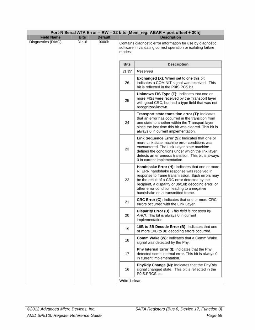
©2012 Advanced Micro Devices, Inc. SATA Registers (Bus 0, Device 17, Function 0) AMD SP5100 Register Reference Guide Page 59
Port-N Serial ATA Error – RW – 32 bits [Mem_reg: ABAR + port offset + 30h] Field Name Bits Default Description
Diagnostics (DIAG) 31:16 0000h Contains diagnostic error information for use by diagnostic software in validating correct operation or isolating failure modes:
Bits Description
31:27 Reserved
26 Exchanged (X): When set to one this bit indicates a COMINIT signal was received. This bit is reflected in the P0IS.PCS bit.
25
Unknown FIS Type (F): Indicates that one or more FISs were received by the Transport layer with good CRC, but had a type field that was not recognized/known.
24
Transport state transition error (T): Indicates that an error has occurred in the transition from one state to another within the Transport layer since the last time this bit was cleared. This bit is always 0 in current implementation.
23
Link Sequence Error (S): Indicates that one or more Link state machine error conditions was encountered. The Link Layer state machine defines the conditions under which the link layer detects an erroneous transition. This bit is always 0 in current implementation.
22
Handshake Error (H): Indicates that one or more R_ERR handshake response was received in response to frame transmission. Such errors may be the result of a CRC error detected by the recipient, a disparity or 8b/10b decoding error, or other error condition leading to a negative handshake on a transmitted frame.
21 CRC Error (C): Indicates that one or more CRC errors occurred with the Link Layer.
20 Disparity Error (D): This field is not used by AHCI. This bit is always 0 in current implementation.
19 10B to 8B Decode Error (B): Indicates that one or more 10B to 8B decoding errors occurred.
18 Comm Wake (W): Indicates that a Comm Wake signal was detected by the Phy.
17 Phy Internal Error (I): Indicates that the Phy detected some internal error. This bit is always 0 in current implementation.
16 PhyRdy Change (N): Indicates that the PhyRdy signal changed state. This bit is reflected in the P0IS.PRCS bit.
Write 1 clear.
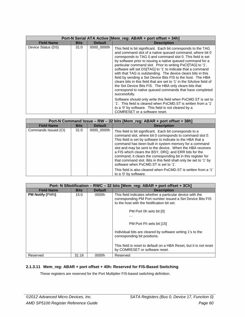
©2012 Advanced Micro Devices, Inc. SATA Registers (Bus 0, Device 17, Function 0) AMD SP5100 Register Reference Guide Page 60
Port-N Serial ATA Active [Mem_reg: ABAR + port offset + 34h] Field Name Bits Default Description
Device Status (DS) 31:0 0000_0000h This field is bit significant. Each bit corresponds to the TAG and command slot of a native queued command, where bit 0 corresponds to TAG 0 and command slot 0. This field is set by software prior to issuing a native queued command for a particular command slot. Prior to writing PxCI[TAG] to ‘1’, software will set DS[TAG] to ‘1’ to indicate that a command with that TAG is outstanding. The device clears bits in this field by sending a Set Device Bits FIS to the host. The HBA clears bits in this field that are set to ‘1’ in the SActive field of the Set Device Bits FIS. The HBA only clears bits that correspond to native queued commands that have completed successfully. Software should only write this field when PxCMD.ST is set to ‘1’. This field is cleared when PxCMD.ST is written from a ‘1’ to a ‘0’ by software. This field is not cleared by a COMRESET or a software reset.
Port-N Command Issue – RW – 32 bits [Mem_reg: ABAR + port offset + 38h]
Field Name Bits Default Description Commands Issued (CI) 31:0 0000_0000h This field is bit significant. Each bit corresponds to a
command slot, where bit 0 corresponds to command slot 0. This field is set by software to indicate to the HBA that a command has been built in system memory for a command slot and may be sent to the device. When the HBA receives a FIS which clears the BSY, DRQ, and ERR bits for the command, it clears the corresponding bit in this register for that command slot. Bits in this field shall only be set to ‘1’ by software when PxCMD.ST is set to ‘1’. This field is also cleared when PxCMD.ST is written from a ‘1’ to a ‘0’ by software.
Port- N SNotification – RWC – 32 bits [Mem_reg: ABAR + port offset + 3Ch] Field Name Bits Default Description
PM Notify (PMN) 15:0 0000h This field indicates whether a particular device with the corresponding PM Port number issued a Set Device Bits FIS to the host with the Notification bit set.
PM Port 0h sets bit [0] … PM Port Fh sets bit [15]
Individual bits are cleared by software writing 1’s to the corresponding bit positions. This field is reset to default on a HBA Reset, but it is not reset by COMRESET or software reset.
Reserved 31:16 0000h Reserved
2.1.3.11 Mem_reg: ABAR + port offset + 40h: Reserved for FIS-Based Switching These registers are reserved for the Port Multiplier FIS-based switching definition.
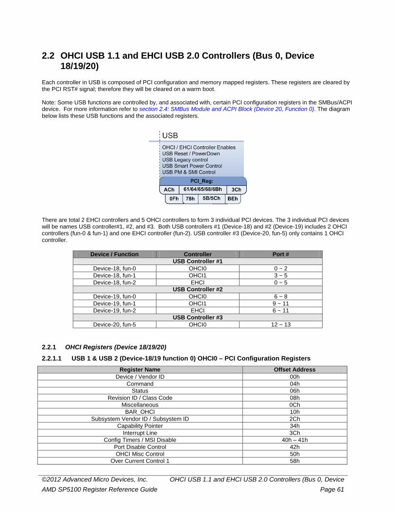
©2012 Advanced Micro Devices, Inc. OHCI USB 1.1 and EHCI USB 2.0 Controllers (Bus 0, Device AMD SP5100 Register Reference Guide Page 61
2.2 OHCI USB 1.1 and EHCI USB 2.0 Controllers (Bus 0, Device 18/19/20)
Each controller in USB is composed of PCI configuration and memory mapped registers. These registers are cleared by the PCI RST# signal; therefore they will be cleared on a warm boot. Note: Some USB functions are controlled by, and associated with, certain PCI configuration registers in the SMBus/ACPI device. For more information refer to section 2.4: SMBus Module and ACPI Block (Device 20, Function 0). The diagram below lists these USB functions and the associated registers.
There are total 2 EHCI controllers and 5 OHCI controllers to form 3 individual PCI devices. The 3 individual PCI devices will be names USB controller#1, #2, and #3. Both USB controllers #1 (Device-18) and #2 (Device-19) includes 2 OHCI controllers (fun-0 & fun-1) and one EHCI controller (fun-2). USB controller #3 (Device-20, fun-5) only contains 1 OHCI controller.
Device / Function Controller Port # USB Controller #1
Device-18, fun-0 OHCI0 0 ~ 2 Device-18, fun-1 OHCI1 3 ~ 5 Device-18, fun-2 EHCI 0 ~ 5
USB Controller #2 Device-19, fun-0 OHCI0 6 ~ 8 Device-19, fun-1 OHCI1 9 ~ 11 Device-19, fun-2 EHCI 6 ~ 11
USB Controller #3 Device-20, fun-5 OHCI0 12 ~ 13
2.2.1 OHCI Registers (Device 18/19/20)
2.2.1.1 USB 1 & USB 2 (Device-18/19 function 0) OHCI0 – PCI Configuration Registers Register Name Offset Address
Device / Vendor ID 00h Command 04h
Status 06h Revision ID / Class Code 08h
Miscellaneous 0Ch BAR_OHCI 10h
Subsystem Vendor ID / Subsystem ID 2Ch Capability Pointer 34h
Interrupt Line 3Ch Config Timers / MSI Disable 40h – 41h
Port Disable Control 42h OHCI Misc Control 50h
Over Current Control 1 58h
©2012 Advanced Micro Devices, Inc. OHCI USB 1.1 and EHCI USB 2.0 Controllers (Bus 0, Device AMD SP5100 Register Reference Guide Page 62
Register Name Offset Address OHCI OverCurrentPME Enable 68h
Target Timeout Control 74h MSI Control D0h MSI Address D4h
MSI Data D8h HT MSI Support E4h
2.2.1.2 USB1 & USB2 (Device-18/19 function 1) OHCI 1 – PCI Configuration Registers Register Name Offset Address
Device / Vendor ID 00h Command 04h
Status 06h Revision ID / Class Code 08h
Miscellaneous 0Ch BAR_OHCI 10h
Subsystem Vendor ID / Subsystem ID 2Ch Capability Pointer 34h
Interrupt Line 3Ch MSI Control D0h MSI Address D4h
MSI Data D8h Note : The PCI_Reg x40 ~ x7C only exists in the OHCI0, but not in any other OHCI controllers.
Device / Vendor ID – R - 32 bits - [PCI_Reg : 00h] Field Name Bits Default Description
VEND_ID 15:0 1002h Vendor ID DEV_ID 31:16 Function 0: 4397h
Function 1: 4398h
Device ID
Command – RW - 16 bits - [PCI_Reg : 04h] Field Name Bits Default Description
IO Space Accesses
0 0b A value of 0 disables the device response. A value of 1 allows the device to respond to I/O Space accesses.
Memory Space Accesses
1 0b A value of 0 disables the device response. A value of 1 allows the device to respond to Memory Space accesses.
Bus Master 2 0b A value of 0 disables the device from generating PCI accesses. A value of 1 allows the device to behave as a bus master.
Special Cycle 3 0b Hardwired to 0, indicating no Special Cycle support. Memory Write and Invalidate Command
4 0b When it is 0, Memory Write must be used. When it is 1, masters may generate the command.
VGA Palette Register Accesses
5 0b Hardwired to 0, indicating the device should treat palette write accesses like all other accesses.
Parity Enable 6 0b When it is 1, the device must take its normal action when a parity error is detected. When it is 0, the device sets its Detected Parity Error status bit (bit 15 in the Status register) when an error is detected, but continues normal operations without asserting PERR#.
Reserved 7 0b Hardwired to 0 per PCI2.3 spec.
©2012 Advanced Micro Devices, Inc. OHCI USB 1.1 and EHCI USB 2.0 Controllers (Bus 0, Device AMD SP5100 Register Reference Guide Page 63
Command – RW - 16 bits - [PCI_Reg : 04h] Field Name Bits Default Description
SERR# Enable 8 0b A value of 0 disables the SERR# driver. A value of 1 enables the SERR# driver. Address parity errors are reported only if this bit and bit [6] are 1.
Fast Back-to-Back Enable
9 0b A value of 0 means only fast back-to-back transactions to the same agent are allowed. A value of 1 means the master is allowed to generate fast back-to-back transactions to different agents.
Interrupt Disable 10 0b A value of 0 enables the assertion of the device/function’s INTx# signal. A value of 1 disables the assertion of the device/function’s INTx# signal.
Reserved 15:11 Reserved
Status – R - 16 bits - [PCI_Reg : 06h] Field Name Bits Default Description
Reserved 2:0 Reserved Interrupt Status 3 0b This bit reflects the state of the interrupt in the device/function. Only
when the Interrupt Disable bit in the command register is a 0 and this Interrupt Status bit is a 1 will the device’s/function’s INTx# signal be asserted. Setting the Interrupt Disable bit to a 1 has no effect on the state of this bit.
Capabilities List 4 1b A value of 0 indicates that no New Capabilities linked list is available. A value of 1 indicates that the value read at offset 34h is a pointer in Configuration Space to a linked list of new capabilities.
66 MHz Capable 5 1b Hardwired to 1, indicating 66MHz capable. Reserved 6 Reserved Fast Back-to-Back Capable
7 1b Hard-wired to 1, indicating Fast Back-to-Back capable.
Master Data Parity Error
8 0b This bit is set only when three conditions are met: (1) the bus agent asserted PERR# itself (on a read) or observed PERR# asserted (on a write); (2) the agent setting the bit acted as the bus master for the operation in which the error occurred; and (3) the Parity Error Response bit (Command register) is set.
DEVSEL timing 10:9 01b Hardwired to 01b – medium timing Signaled Target Abort
11 0b This bit is set by a target device whenever it terminates a transaction with Target-Abort.
Received Target Abort
12 0b This bit is set by a master device whenever its transaction is terminated with Target-Abort.
Received Master Abort
13 0b This bit is set by a master device whenever its transaction (except for Special Cycle) is terminated with Master-Abort.
Signaled System Error
14 0b This bit is set whenever the device asserts SERR#.
Detected Parity Error
15 0b This bit is set by the device whenever it detects a parity error, even if parity error handling is disabled (as controlled by bit 6 in the Command register).
Revision ID / Class Code – R - 32 bits - [PCI_Reg : 08h] Field Name Bits Default Description
Revision ID 7:0 00h Revision ID. PI 15:8 10h Programming Interface. A constant value of ‘10h’ indentifies the device
being an OpenHCI Host Controller. SC 23:16 03h Sub Class. A constant value of ‘03h’ indentifies the device being of
Universal Serial Bus. BC 31:24 0Ch Base Class. A constant value of ‘0Ch’ identifies the device being a Serial
Bus Controller.
©2012 Advanced Micro Devices, Inc. OHCI USB 1.1 and EHCI USB 2.0 Controllers (Bus 0, Device AMD SP5100 Register Reference Guide Page 64
Miscellaneous – RW/R - 32 bits - [PCI_Reg : 0Ch] Field Name Bits Default Description
Cache Line Size 7:0 00h This read/write field specifies the system cacheline size in units of DWORDs and must be initialized to 00h.
Latency Timer 15:8 00h [9:8] hard-wired to 00b, resulting in a timer granularity of at least four clocks. This field specifies, in units of PCI bus clocks, the value of the Latency Timer for this PCI bus master.
Header Type 23:16 80h/00h This field identifies the layout of the second part of the predefined header (beginning at byte 10h in Configuration Space) and also whether or not the device contains multiple functions. Function 0: Bit [23] hardwired to 1 the device has multiple functions. Function 1: Bit [23] hardwired to 0 the device is single function. Bits [22:16]: Hard-wired to 00h.
BIST 31:24 00h Hardwired to 00h, indicating no build-in BIST support.
Bar_OHCI – RW - 32 bits - [PCI_Reg : 10h] Field Name Bits Default Description
IND 0 0b Indicator. A constant value of ‘0’ indicates that the operational registers of the device are mapped into memory space of the main memory of the PC host system. Read Only.
TP 2:1 0h Type. A constant value of ‘00b’ indicates that the base register is 32-bit wide and can be placed anywhere in the 32-bit memory space; i.e., lower 4 GB of the main memory of the PC host. Read Only.
PM 3 0b Prefetch memory. A constant value of ‘0’ indicates that there is no support for “prefetchable memory”. Read Only.
11:4 00h Represents a maximum of 4-KB addressing space for the OpenHCi’s operational registers. Read Only.
BAR 31:12 000h Base Address. Specifies the upper 20 bits of the 32-bit starting base address. This represent a maximum of 4-KB addressing space for the OpenHCI’s operational registers.
Subsystem Vendor ID / Subsystem ID – RW - 32 bits - [PCI_Reg : 2Ch] Field Name Bits Default Description
Subsystem Vendor ID 15:0 0000h Can only be written once by software. Subsystem ID 31:16 0000h Can only be written once by software.
Capability Pointer – R - 8 bits - [PCI_Reg : 34h] Field Name Bits Default Description
Capability Pointer 7:0 D0h Address of the 1st element of capability link.

©2012 Advanced Micro Devices, Inc. OHCI USB 1.1 and EHCI USB 2.0 Controllers (Bus 0, Device AMD SP5100 Register Reference Guide Page 65
Interrupt Line – RW – 32 bits - [PCI_Reg : 3Ch] Field Name Bits Default Description
Interrupt Line 7:0 00h The Interrupt Line register is an eight-bit register used to communicate interrupt line routing information. The register is read/write and must be implemented by any device (or device function) that uses an interrupt pin. POST software will write the routing information into this register as it initializes and configures the system. The value in this register tells which input of the system interrupt controller(s) the device's interrupt pin is connected to. The device itself does not use this value; rather it is used by device drivers and operating systems. Device drivers and operating systems can use this information to determine priority and vector information. Values in this register are system architecture specific.
Interrupt Pin 15:8 01h
Read Only by default. OHCI0: Hard-wired to 01h, corresponding to using INTA#. OHCI1: Hard-wired to 01h, corresponding to using INTA#.
MIN_GNT 23:16 00h Read Only. Hardwired to 00h to indicate no major requirements for the settings of Latency Timers.
MAX_LAT 31:24 00h Read Only. Hardwired to 00h to indicate no major requirements for the settings of Latency Timers.
If Interrupt Backdoor Enable bit (OHCI0 regx50[7]) is set, this field is writable.
Config Timers / MSI Disable (OHCI0 only) – RW - 16 bits - [PCI_Reg : 40h] Field Name Bits Default Description
TRDY Timer 7:0 80h Target Ready timer to timeout non-responding target. MSI Disable 9:8 00h When these bits are set MSI capability will be disabled for
the corresponding Host Controller. Bit [8]: OHCI0 Bit [9]: OHCI1
Reserved 15:10 0h Reserved
Port Disable (OHCI0 only) – RW* - 16 bits - [PCI_Reg : 42h] Field Name Bits Default Description
Port_disable
5:0
00h When these bits are set the corresponding ports are disabled. For example, if bit-0 is set then port-0 (its corresponding port) is disabled; if bit-1 is set, then its corresponding port (port-1) is disabled (and so on). Only value ‘1’ can be written into the register. The bit can be cleared to ‘0’ by system reset (PciRst#). In other words, when the bit is set to ‘1’, the value is locked and cannot be cleared by any software write.
Reserved 15:6 00h Reserved Note: Only writing value ‘1’ take effect to the register value, software writes ‘0’ take no effect. The register can only be clear by hardware reset.
OHCI Misc Control (OHCI0 only) – RW - 16 bits - [PCI_Reg: 50h] Field Name Bits Default Description
OHCI Dynamic Power Saving Enable
0
0b When this bit is set Dynamic Power Saving for OHCI is enabled. By default, the power saving function is disabled.
Reserved 7:1 00h Reserved
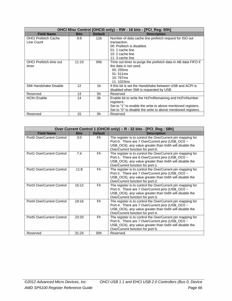
©2012 Advanced Micro Devices, Inc. OHCI USB 1.1 and EHCI USB 2.0 Controllers (Bus 0, Device AMD SP5100 Register Reference Guide Page 66
OHCI Misc Control (OHCI0 only) – RW - 16 bits - [PCI_Reg: 50h] Field Name Bits Default Description
OHCI Prefetch Cache Line Count
9:8 11b Number of data cache line prefetch request for ISO out transaction. 00: Prefetch is disabled. 01: 1 cache line 10: 2 cache line 11: 3 cache line
OHCI Prefetch time out timer
11:10 00b Time out timer to purge the prefetch data in AB data FIFO if the data is not used. 00: 255ms 01: 511ms 10: 767ms 11: 1023ms
SMI Handshake Disable 12 1b If this bit is set the Handshake between USB and ACPI is disabled when SMI is requested by USB
Reserved 13 0h Reserved HCfm Enable 14 0b Enable bit to write the HcFmRemaining and HcFmNumber
registers. Set to "1" to enable the write to above mentioned registers. Set to "0" to disable the write to above mentioned registers.
Reserved 15 0h Reserved
Over Current Control 1 (OHCI0 only) – R - 32 bits - [PCI_Reg : 58h] Field Name Bits Default Description
Port0 OverCurrent Control 3:0 Fh The register is to control the OverCurrent pin mapping for Port-0. There are 7 OverCurrent pins (USB_OC0 ~ USB_OC6), any value greater than 0x6h will disable the OverCurrent function for port-0.
Port1 OverCurrent Control 7:4 Fh The register is to control the OverCurrent pin mapping for Port-1. There are 6 OverCurrent pins (USB_OC0 ~ USB_OC6), any value greater than 0x6h will disable the OverCurrent function for port-1.
Port2 OverCurrent Control 11:8 Fh The register is to control the OverCurrent pin mapping for Port-2. There are 7 OverCurrent pins (USB_OC0 ~ USB_OC6), any value greater than 0x6h will disable the OverCurrent function for port-2.
Port3 OverCurrent Control 15:12 Fh The register is to control the OverCurrent pin mapping for Port-3. There are 7 OverCurrent pins (USB_OC0 ~ USB_OC6), any value greater than 0x6h will disable the OverCurrent function for port-3.
Port4 OverCurrent Control 19:16 Fh The register is to control the OverCurrent pin mapping for Port-4. There are 7 OverCurrent pins (USB_OC0 ~ USB_OC6), any value greater than 0x6h will disable the OverCurrent function for port-4.
Port5 OverCurrent Control 23:20 Fh The register is to control the OverCurrent pin mapping for Port-5. There are 7 OverCurrent pins (USB_OC0 ~ USB_OC6), any value greater than 0x6h will disable the OverCurrent function for port-5.
Reserved 31:24 00h Reserved.
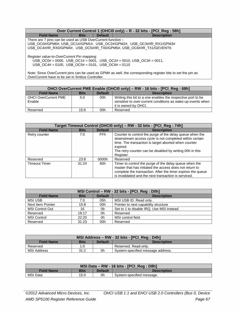
©2012 Advanced Micro Devices, Inc. OHCI USB 1.1 and EHCI USB 2.0 Controllers (Bus 0, Device AMD SP5100 Register Reference Guide Page 67
Over Current Control 1 (OHCI0 only) – R - 32 bits - [PCI_Reg : 58h] Field Name Bits Default Description
There are 7 pins can be used as USB OverCurrent function – USB_OC0#/GPM0#, USB_OC1#/GPM1#, USB_OC2#/GPM2#, USB_OC3#/IR_RX1/GPM3# USB_OC4#/IR_RX0/GPM4#, USB_OC5#/IR_TX0/GPM5#, USB_OC6#/IR_TX1/GEVENT6 Register value-to-OverCurrent Pin mapping: USB_OC0# = 0000, USB_OC1# = 0001, USB_OC2# = 0010, USB_OC3# = 0011, USB_OC4# = 0100, USB_OC5# = 0101, USB_OC6# = 0110 Note: Since OverCurrent pins can be used as GPM# as well, the corresponding register bits to set the pin as OverCurrent have to be set in Smbus Controller.
OHCI OverCurrent PME Enable (OHCI0 only) – RW - 16 bits - [PCI_Reg : 68h] Field Name Bits Default Description
OHCI OverCurrent PME Enable
5:0 00h Writing this bit to a one enables the respective port to be sensitive to over-current conditions as wake-up events when it is owned by OHCI.
Reserved 15:6 00h Reserved
Target Timeout Control (OHCI0 only) – RW - 32 bits - [PCI_Reg : 74h] Field Name Bits Default Description
Retry counter 7:0 FFh Counter to control the purge of the delay queue when the downstream access cycle is not completed within certain time. The transaction is target aborted when counter expired. The retry counter can be disabled by writing 00h in this Register.
Reserved 23:8 0000h Reserved Timeout Timer 31:24 80h Timer to control the purge of the delay queue when the
master that has initiated the access does not return to complete the transaction. After the timer expires the queue is invalidated and the next transaction is serviced.
MSI Control – RW - 32 bits - [PCI_Reg : D0h] Field Name Bits Default Description
MSI USB 7:0 05h MSI USB ID. Read only. Next Item Pointer 15:8 00h Pointer to next capability structure MSI Control Out 16 0b Set to 1 to disable IRQ. Use MSI instead. Reserved 19:17 0h Reserved MSI Control 22:20 0h MSI control field Reserved 31:23 00h Reserved
MSI Address – RW - 32 bits - [PCI_Reg : D4h] Field Name Bits Default Description
Reserved 1:0 Reserved. Read-only. MSI Address 31:2 0h System-specified message address.
MSI Data – RW - 16 bits - [PCI_Reg : D8h] Field Name Bits Default Description
MSI Data 15:0 0h System-specified message.

©2012 Advanced Micro Devices, Inc. OHCI USB 1.1 and EHCI USB 2.0 Controllers (Bus 0, Device AMD SP5100 Register Reference Guide Page 68
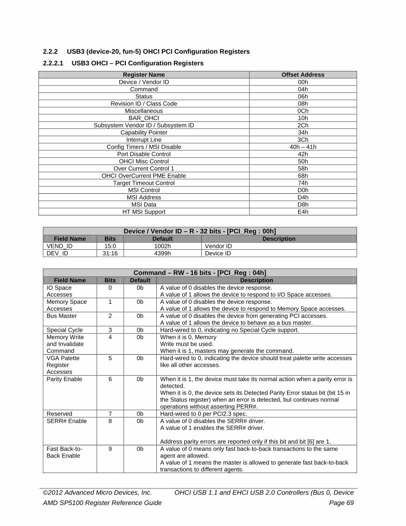
©2012 Advanced Micro Devices, Inc. OHCI USB 1.1 and EHCI USB 2.0 Controllers (Bus 0, Device AMD SP5100 Register Reference Guide Page 69
2.2.2 USB3 (device-20, fun-5) OHCI PCI Configuration Registers
2.2.2.1 USB3 OHCI – PCI Configuration Registers Register Name Offset Address
Device / Vendor ID 00h Command 04h
Status 06h Revision ID / Class Code 08h
Miscellaneous 0Ch BAR_OHCI 10h
Subsystem Vendor ID / Subsystem ID 2Ch Capability Pointer 34h
Interrupt Line 3Ch Config Timers / MSI Disable 40h – 41h
Port Disable Control 42h OHCI Misc Control 50h
Over Current Control 1 58h OHCI OverCurrent PME Enable 68h
Target Timeout Control 74h MSI Control D0h MSI Address D4h
MSI Data D8h HT MSI Support E4h
Device / Vendor ID – R - 32 bits - [PCI_Reg : 00h] Field Name Bits Default Description
VEND_ID 15:0 1002h Vendor ID DEV_ID 31:16 4399h Device ID
Command – RW - 16 bits - [PCI_Reg : 04h] Field Name Bits Default Description
IO Space Accesses
0 0b A value of 0 disables the device response. A value of 1 allows the device to respond to I/O Space accesses.
Memory Space Accesses
1 0b A value of 0 disables the device response. A value of 1 allows the device to respond to Memory Space accesses.
Bus Master 2 0b A value of 0 disables the device from generating PCI accesses. A value of 1 allows the device to behave as a bus master.
Special Cycle 3 0b Hard-wired to 0, indicating no Special Cycle support. Memory Write and Invalidate Command
4 0b When it is 0, Memory Write must be used. When it is 1, masters may generate the command.
VGA Palette Register Accesses
5 0b Hard-wired to 0, indicating the device should treat palette write accesses like all other accesses.
Parity Enable 6 0b When it is 1, the device must take its normal action when a parity error is detected. When it is 0, the device sets its Detected Parity Error status bit (bit 15 in the Status register) when an error is detected, but continues normal operations without asserting PERR#.
Reserved 7 0b Hard-wired to 0 per PCI2.3 spec. SERR# Enable 8 0b A value of 0 disables the SERR# driver.
A value of 1 enables the SERR# driver. Address parity errors are reported only if this bit and bit [6] are 1.
Fast Back-to-Back Enable
9 0b A value of 0 means only fast back-to-back transactions to the same agent are allowed. A value of 1 means the master is allowed to generate fast back-to-back transactions to different agents.
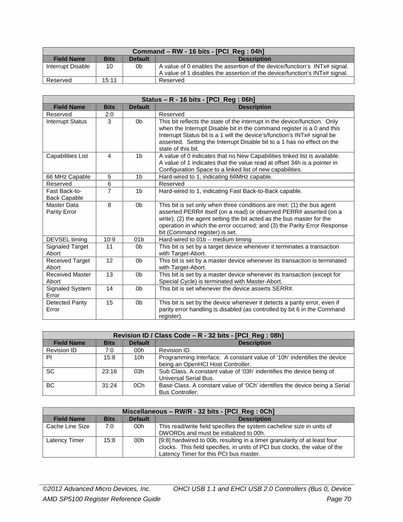
©2012 Advanced Micro Devices, Inc. OHCI USB 1.1 and EHCI USB 2.0 Controllers (Bus 0, Device AMD SP5100 Register Reference Guide Page 70
Command – RW - 16 bits - [PCI_Reg : 04h] Field Name Bits Default Description
Interrupt Disable 10 0b A value of 0 enables the assertion of the device/function’s INTx# signal. A value of 1 disables the assertion of the device/function’s INTx# signal.
Reserved 15:11 Reserved
Status – R - 16 bits - [PCI_Reg : 06h] Field Name Bits Default Description
Reserved 2:0 Reserved Interrupt Status 3 0b This bit reflects the state of the interrupt in the device/function. Only
when the Interrupt Disable bit in the command register is a 0 and this Interrupt Status bit is a 1 will the device’s/function’s INTx# signal be asserted. Setting the Interrupt Disable bit to a 1 has no effect on the state of this bit.
Capabilities List 4 1b A value of 0 indicates that no New Capabilities linked list is available. A value of 1 indicates that the value read at offset 34h is a pointer in Configuration Space to a linked list of new capabilities.
66 MHz Capable 5 1b Hard-wired to 1, indicating 66MHz capable. Reserved 6 Reserved Fast Back-to-Back Capable
7 1b Hard-wired to 1, indicating Fast Back-to-Back capable.
Master Data Parity Error
8 0b This bit is set only when three conditions are met: (1) the bus agent asserted PERR# itself (on a read) or observed PERR# asserted (on a write); (2) the agent setting the bit acted as the bus master for the operation in which the error occurred; and (3) the Parity Error Response bit (Command register) is set.
DEVSEL timing 10:9 01b Hard-wired to 01b – medium timing Signaled Target Abort
11 0b This bit is set by a target device whenever it terminates a transaction with Target-Abort.
Received Target Abort
12 0b This bit is set by a master device whenever its transaction is terminated with Target-Abort.
Received Master Abort
13 0b This bit is set by a master device whenever its transaction (except for Special Cycle) is terminated with Master-Abort.
Signaled System Error
14 0b This bit is set whenever the device asserts SERR#.
Detected Parity Error
15 0b This bit is set by the device whenever it detects a parity error, even if parity error handling is disabled (as controlled by bit 6 in the Command register).
Revision ID / Class Code – R - 32 bits - [PCI_Reg : 08h] Field Name Bits Default Description
Revision ID 7:0 00h Revision ID. PI 15:8 10h Programming Interface. A constant value of ‘10h’ indentifies the device
being an OpenHCI Host Controller. SC 23:16 03h Sub Class. A constant value of ‘03h’ indentifies the device being of
Universal Serial Bus. BC 31:24 0Ch Base Class. A constant value of ‘0Ch’ identifies the device being a Serial
Bus Controller.
Miscellaneous – RW/R - 32 bits - [PCI_Reg : 0Ch] Field Name Bits Default Description
Cache Line Size 7:0 00h This read/write field specifies the system cacheline size in units of DWORDs and must be initialized to 00h.
Latency Timer 15:8 00h [9:8] hardwired to 00b, resulting in a timer granularity of at least four clocks. This field specifies, in units of PCI bus clocks, the value of the Latency Timer for this PCI bus master.
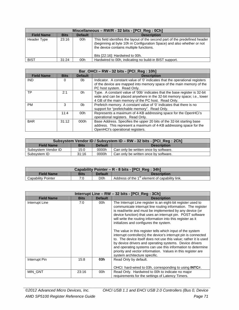
©2012 Advanced Micro Devices, Inc. OHCI USB 1.1 and EHCI USB 2.0 Controllers (Bus 0, Device AMD SP5100 Register Reference Guide Page 71
Miscellaneous – RW/R - 32 bits - [PCI_Reg : 0Ch] Field Name Bits Default Description
Header Type 23:16 00h This field identifies the layout of the second part of the predefined header (beginning at byte 10h in Configuration Space) and also whether or not the device contains multiple functions. Bits [22:16]: Hardwired to 00h.
BIST 31:24 00h Hardwired to 00h, indicating no build-in BIST support.
Bar_OHCI – RW - 32 bits - [PCI_Reg : 10h] Field Name Bits Default Description
IND 0 0b Indicator. A constant value of ‘0’ indicates that the operational registers of the device are mapped into memory space of the main memory of the PC host system. Read Only.
TP 2:1 0h Type. A constant value of ‘00b’ indicates that the base register is 32-bit wide and can be placed anywhere in the 32-bit memory space; i.e., lower 4 GB of the main memory of the PC host. Read Only.
PM 3 0b Prefetch memory. A constant value of ‘0’ indicates that there is no support for “prefetchable memory”. Read Only.
11:4 00h Represents a maximum of 4-KB addressing space for the OpenHCi’s operational registers. Read Only.
BAR 31:12 000h Base Address. Specifies the upper 20 bits of the 32-bit starting base address. This represent a maximum of 4-KB addressing space for the OpenHCI’s operational registers.
Subsystem Vendor ID / Subsystem ID – RW - 32 bits - [PCI_Reg : 2Ch] Field Name Bits Default Description
Subsystem Vendor ID 15:0 0000h Can only be written once by software. Subsystem ID 31:16 0000h Can only be written once by software.
Capability Pointer – R - 8 bits - [PCI_Reg : 34h] Field Name Bits Default Description
Capability Pointer 7:0 D0h Address of the 1st element of capability link.
Interrupt Line – RW – 32 bits - [PCI_Reg : 3Ch] Field Name Bits Default Description
Interrupt Line 7:0 00h The Interrupt Line register is an eight-bit register used to communicate interrupt line routing information. The register is read/write and must be implemented by any device (or device function) that uses an interrupt pin. POST software will write the routing information into this register as it initializes and configures the system. The value in this register tells which input of the system interrupt controller(s) the device's interrupt pin is connected to. The device itself does not use this value; rather it is used by device drivers and operating systems. Device drivers and operating systems can use this information to determine priority and vector information. Values in this register are system architecture specific.
Interrupt Pin 15:8 03h Read Only by default. OHCI: hard-wired to 03h, corresponding to using INTC#.
MIN_GNT 23:16 00h Read Only. Hardwired to 00h to indicate no major requirements for the settings of Latency Timers.
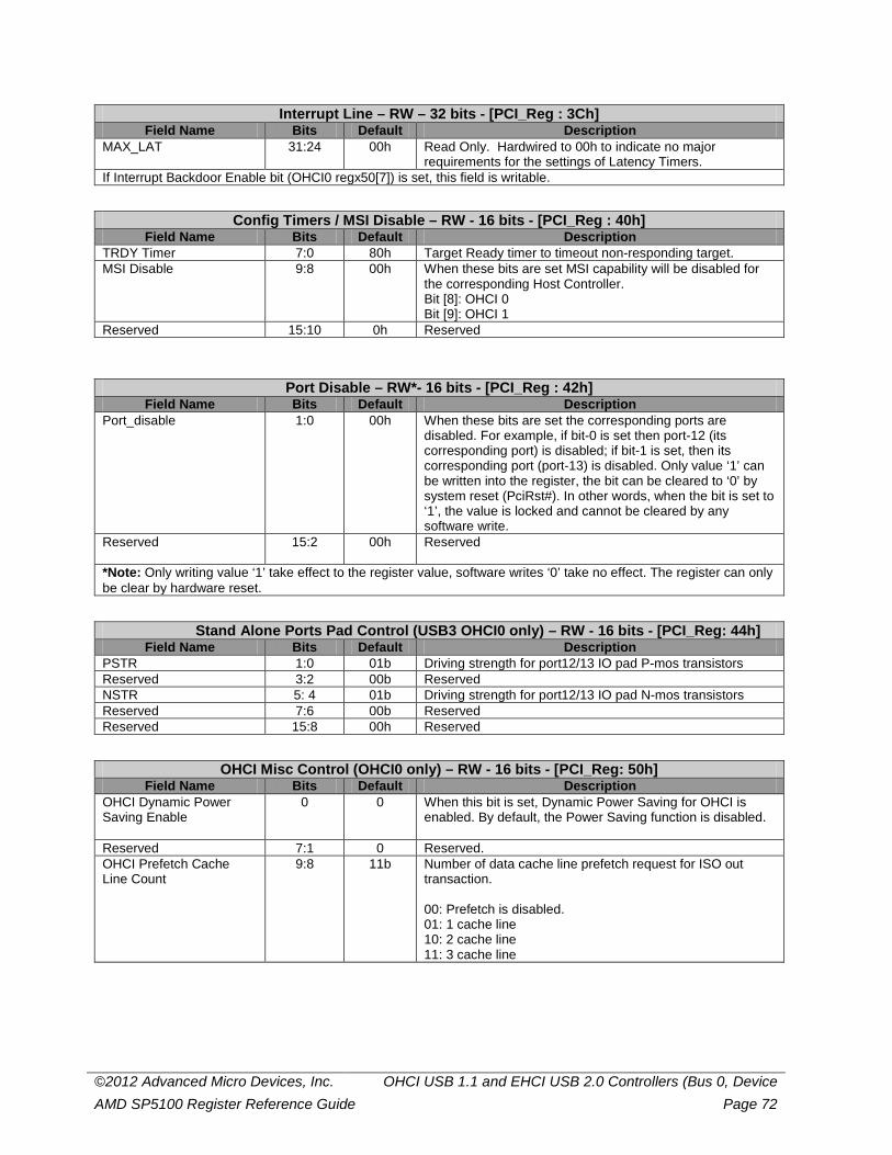
©2012 Advanced Micro Devices, Inc. OHCI USB 1.1 and EHCI USB 2.0 Controllers (Bus 0, Device AMD SP5100 Register Reference Guide Page 72
Interrupt Line – RW – 32 bits - [PCI_Reg : 3Ch] Field Name Bits Default Description
MAX_LAT 31:24 00h Read Only. Hardwired to 00h to indicate no major requirements for the settings of Latency Timers.
If Interrupt Backdoor Enable bit (OHCI0 regx50[7]) is set, this field is writable.
Config Timers / MSI Disable – RW - 16 bits - [PCI_Reg : 40h] Field Name Bits Default Description
TRDY Timer 7:0 80h Target Ready timer to timeout non-responding target. MSI Disable 9:8 00h When these bits are set MSI capability will be disabled for
the corresponding Host Controller. Bit [8]: OHCI 0 Bit [9]: OHCI 1
Reserved 15:10 0h Reserved
Port Disable – RW*- 16 bits - [PCI_Reg : 42h] Field Name Bits Default Description
Port_disable
1:0
00h When these bits are set the corresponding ports are disabled. For example, if bit-0 is set then port-12 (its corresponding port) is disabled; if bit-1 is set, then its corresponding port (port-13) is disabled. Only value ‘1’ can be written into the register, the bit can be cleared to ‘0’ by system reset (PciRst#). In other words, when the bit is set to ‘1’, the value is locked and cannot be cleared by any software write.
Reserved 15:2 00h Reserved
*Note: Only writing value ‘1’ take effect to the register value, software writes ‘0’ take no effect. The register can only be clear by hardware reset.
Stand Alone Ports Pad Control (USB3 OHCI0 only) – RW - 16 bits - [PCI_Reg: 44h] Field Name Bits Default Description
PSTR 1:0 01b Driving strength for port12/13 IO pad P-mos transistors Reserved 3:2 00b Reserved NSTR 5: 4 01b Driving strength for port12/13 IO pad N-mos transistors Reserved 7:6 00b Reserved Reserved 15:8 00h Reserved
OHCI Misc Control (OHCI0 only) – RW - 16 bits - [PCI_Reg: 50h] Field Name Bits Default Description
OHCI Dynamic Power Saving Enable
0
0 When this bit is set, Dynamic Power Saving for OHCI is enabled. By default, the Power Saving function is disabled.
Reserved 7:1 0 Reserved. OHCI Prefetch Cache Line Count
9:8 11b Number of data cache line prefetch request for ISO out transaction. 00: Prefetch is disabled. 01: 1 cache line 10: 2 cache line 11: 3 cache line
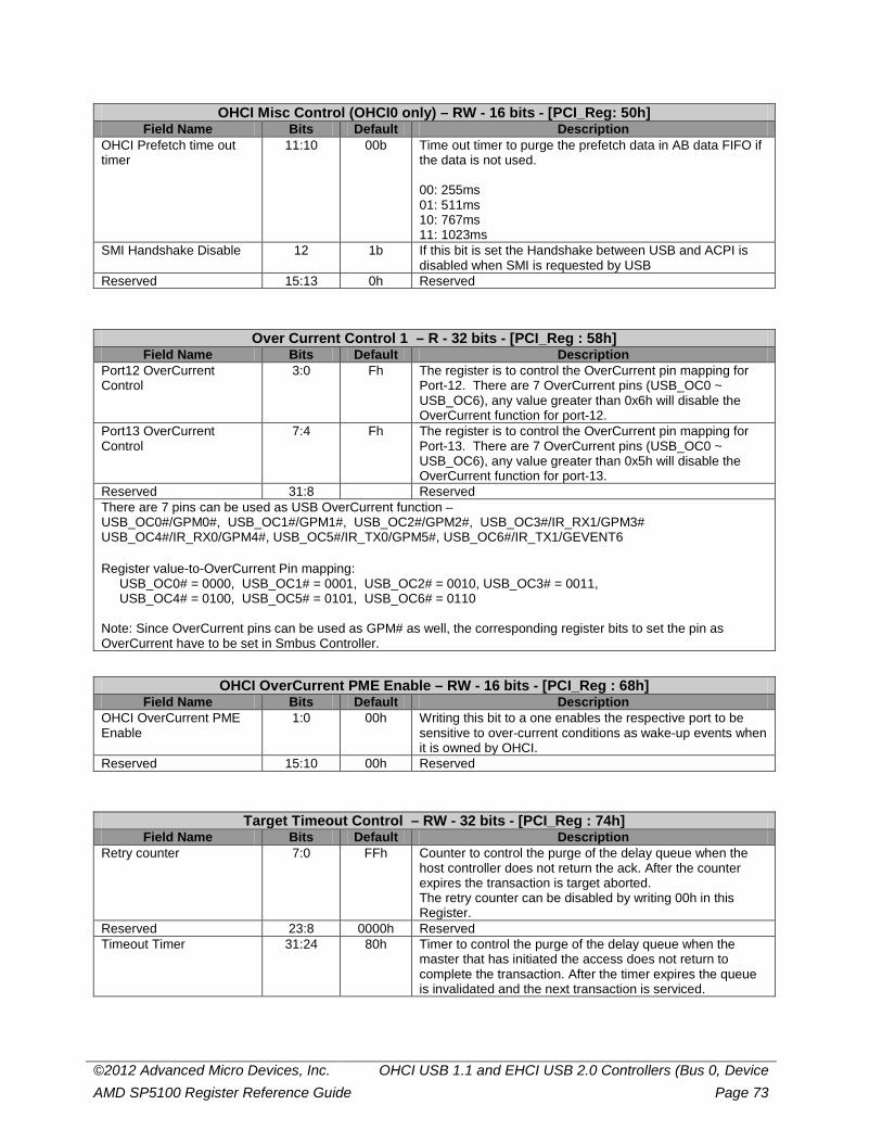
©2012 Advanced Micro Devices, Inc. OHCI USB 1.1 and EHCI USB 2.0 Controllers (Bus 0, Device AMD SP5100 Register Reference Guide Page 73
OHCI Misc Control (OHCI0 only) – RW - 16 bits - [PCI_Reg: 50h] Field Name Bits Default Description
OHCI Prefetch time out timer
11:10 00b Time out timer to purge the prefetch data in AB data FIFO if the data is not used. 00: 255ms 01: 511ms 10: 767ms 11: 1023ms
SMI Handshake Disable 12 1b If this bit is set the Handshake between USB and ACPI is disabled when SMI is requested by USB
Reserved 15:13 0h Reserved
Over Current Control 1 – R - 32 bits - [PCI_Reg : 58h] Field Name Bits Default Description
Port12 OverCurrent Control
3:0 Fh The register is to control the OverCurrent pin mapping for Port-12. There are 7 OverCurrent pins (USB_OC0 ~ USB_OC6), any value greater than 0x6h will disable the OverCurrent function for port-12.
Port13 OverCurrent Control
7:4 Fh The register is to control the OverCurrent pin mapping for Port-13. There are 7 OverCurrent pins (USB_OC0 ~ USB_OC6), any value greater than 0x5h will disable the OverCurrent function for port-13.
Reserved 31:8 Reserved There are 7 pins can be used as USB OverCurrent function – USB_OC0#/GPM0#, USB_OC1#/GPM1#, USB_OC2#/GPM2#, USB_OC3#/IR_RX1/GPM3# USB_OC4#/IR_RX0/GPM4#, USB_OC5#/IR_TX0/GPM5#, USB_OC6#/IR_TX1/GEVENT6 Register value-to-OverCurrent Pin mapping: USB_OC0# = 0000, USB_OC1# = 0001, USB_OC2# = 0010, USB_OC3# = 0011, USB_OC4# = 0100, USB_OC5# = 0101, USB_OC6# = 0110 Note: Since OverCurrent pins can be used as GPM# as well, the corresponding register bits to set the pin as OverCurrent have to be set in Smbus Controller.
OHCI OverCurrent PME Enable – RW - 16 bits - [PCI_Reg : 68h] Field Name Bits Default Description
OHCI OverCurrent PME Enable
1:0 00h Writing this bit to a one enables the respective port to be sensitive to over-current conditions as wake-up events when it is owned by OHCI.
Reserved 15:10 00h Reserved
Target Timeout Control – RW - 32 bits - [PCI_Reg : 74h] Field Name Bits Default Description
Retry counter 7:0 FFh Counter to control the purge of the delay queue when the host controller does not return the ack. After the counter expires the transaction is target aborted. The retry counter can be disabled by writing 00h in this Register.
Reserved 23:8 0000h Reserved Timeout Timer 31:24 80h Timer to control the purge of the delay queue when the
master that has initiated the access does not return to complete the transaction. After the timer expires the queue is invalidated and the next transaction is serviced.
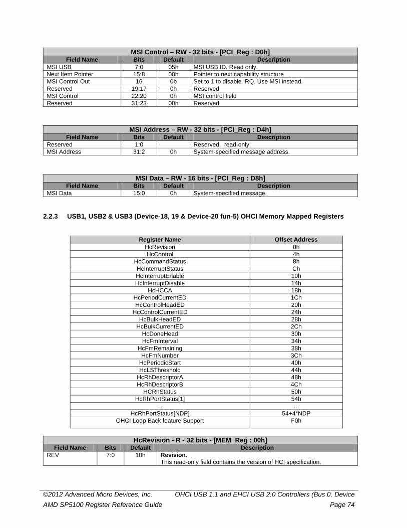
©2012 Advanced Micro Devices, Inc. OHCI USB 1.1 and EHCI USB 2.0 Controllers (Bus 0, Device AMD SP5100 Register Reference Guide Page 74
MSI Control – RW - 32 bits - [PCI_Reg : D0h] Field Name Bits Default Description
MSI USB 7:0 05h MSI USB ID. Read only. Next Item Pointer 15:8 00h Pointer to next capability structure MSI Control Out 16 0b Set to 1 to disable IRQ. Use MSI instead. Reserved 19:17 0h Reserved MSI Control 22:20 0h MSI control field Reserved 31:23 00h Reserved
MSI Address – RW - 32 bits - [PCI_Reg : D4h] Field Name Bits Default Description
Reserved 1:0 Reserved, read-only. MSI Address 31:2 0h System-specified message address.
MSI Data – RW - 16 bits - [PCI_Reg : D8h] Field Name Bits Default Description
MSI Data 15:0 0h System-specified message.
2.2.3 USB1, USB2 & USB3 (Device-18, 19 & Device-20 fun-5) OHCI Memory Mapped Registers
Register Name Offset Address HcRevision 0h HcControl 4h
HcCommandStatus 8h HcInterruptStatus Ch HcInterruptEnable 10h HcInterruptDisable 14h
HcHCCA 18h HcPeriodCurrentED 1Ch HcControlHeadED 20h
HcControlCurrentED 24h HcBulkHeadED 28h
HcBulkCurrentED 2Ch HcDoneHead 30h HcFmInterval 34h
HcFmRemaining 38h HcFmNumber 3Ch
HcPeriodicStart 40h HcLSThreshold 44h
HcRhDescriptorA 48h HcRhDescriptorB 4Ch
HCRhStatus 50h HcRhPortStatus[1] 54h
… … HcRhPortStatus[NDP] 54+4*NDP
OHCI Loop Back feature Support F0h
HcRevision - R - 32 bits - [MEM_Reg : 00h]
Field Name Bits Default Description REV 7:0 10h Revision.
This read-only field contains the version of HCI specification.
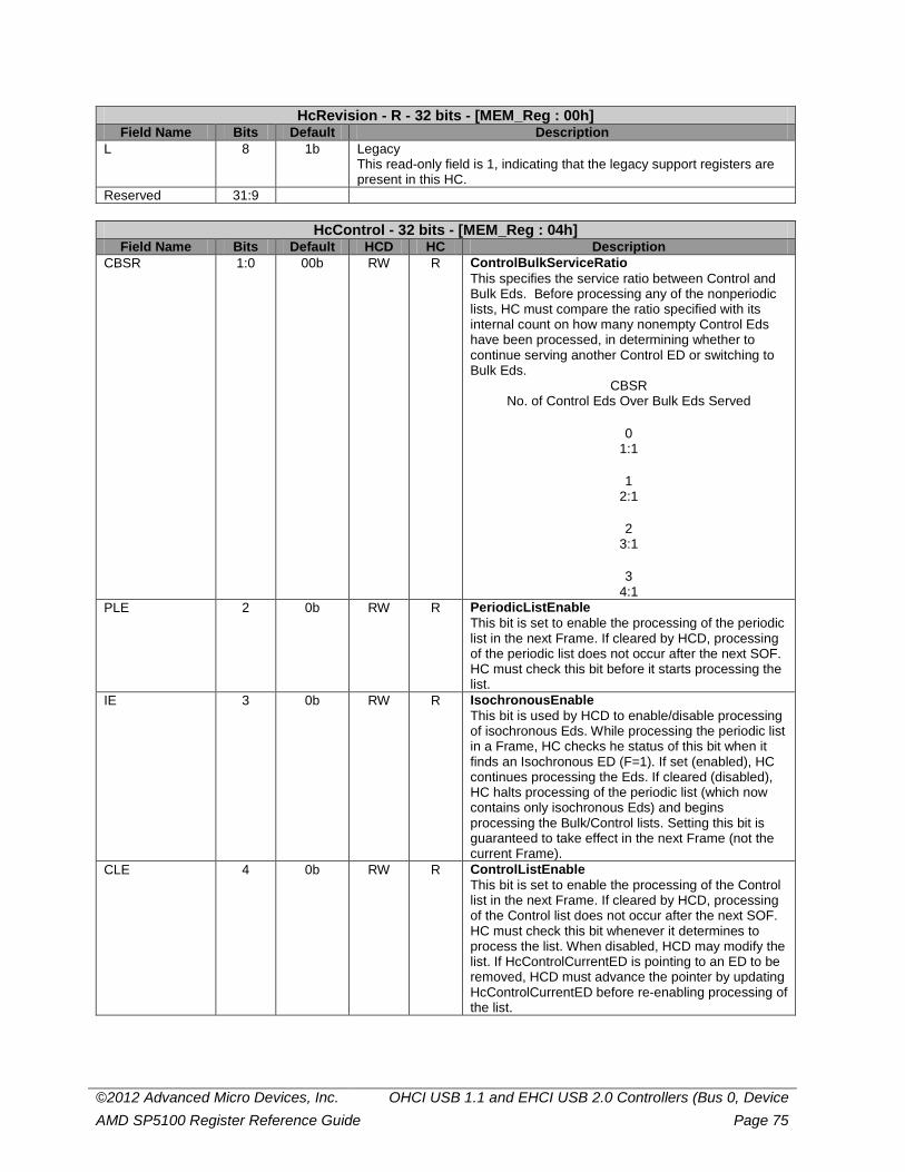
©2012 Advanced Micro Devices, Inc. OHCI USB 1.1 and EHCI USB 2.0 Controllers (Bus 0, Device AMD SP5100 Register Reference Guide Page 75
HcRevision - R - 32 bits - [MEM_Reg : 00h] Field Name Bits Default Description
L 8 1b Legacy This read-only field is 1, indicating that the legacy support registers are present in this HC.
Reserved 31:9
HcControl - 32 bits - [MEM_Reg : 04h] Field Name Bits Default HCD HC Description
CBSR 1:0 00b RW R ControlBulkServiceRatio This specifies the service ratio between Control and Bulk Eds. Before processing any of the nonperiodic lists, HC must compare the ratio specified with its internal count on how many nonempty Control Eds have been processed, in determining whether to continue serving another Control ED or switching to Bulk Eds.
CBSR No. of Control Eds Over Bulk Eds Served
0
1:1
1 2:1
2
3:1
3 4:1
PLE 2 0b RW R PeriodicListEnable This bit is set to enable the processing of the periodic list in the next Frame. If cleared by HCD, processing of the periodic list does not occur after the next SOF. HC must check this bit before it starts processing the list.
IE 3 0b RW R IsochronousEnable This bit is used by HCD to enable/disable processing of isochronous Eds. While processing the periodic list in a Frame, HC checks he status of this bit when it finds an Isochronous ED (F=1). If set (enabled), HC continues processing the Eds. If cleared (disabled), HC halts processing of the periodic list (which now contains only isochronous Eds) and begins processing the Bulk/Control lists. Setting this bit is guaranteed to take effect in the next Frame (not the current Frame).
CLE 4 0b RW R ControlListEnable This bit is set to enable the processing of the Control list in the next Frame. If cleared by HCD, processing of the Control list does not occur after the next SOF. HC must check this bit whenever it determines to process the list. When disabled, HCD may modify the list. If HcControlCurrentED is pointing to an ED to be removed, HCD must advance the pointer by updating HcControlCurrentED before re-enabling processing of the list.
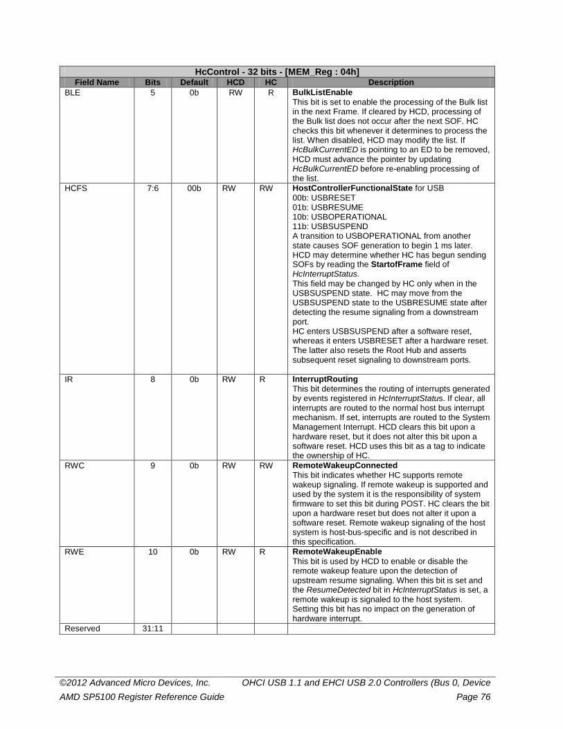
©2012 Advanced Micro Devices, Inc. OHCI USB 1.1 and EHCI USB 2.0 Controllers (Bus 0, Device AMD SP5100 Register Reference Guide Page 76
HcControl - 32 bits - [MEM_Reg : 04h] Field Name Bits Default HCD HC Description
BLE 5 0b RW R BulkListEnable This bit is set to enable the processing of the Bulk list in the next Frame. If cleared by HCD, processing of the Bulk list does not occur after the next SOF. HC checks this bit whenever it determines to process the list. When disabled, HCD may modify the list. If HcBulkCurrentED is pointing to an ED to be removed, HCD must advance the pointer by updating HcBulkCurrentED before re-enabling processing of the list.
HCFS 7:6 00b RW RW HostControllerFunctionalState for USB 00b: USBRESET 01b: USBRESUME 10b: USBOPERATIONAL 11b: USBSUSPEND A transition to USBOPERATIONAL from another state causes SOF generation to begin 1 ms later. HCD may determine whether HC has begun sending SOFs by reading the StartofFrame field of HcInterruptStatus. This field may be changed by HC only when in the USBSUSPEND state. HC may move from the USBSUSPEND state to the USBRESUME state after detecting the resume signaling from a downstream port. HC enters USBSUSPEND after a software reset, whereas it enters USBRESET after a hardware reset. The latter also resets the Root Hub and asserts subsequent reset signaling to downstream ports.
IR 8 0b RW R InterruptRouting This bit determines the routing of interrupts generated by events registered in HcInterruptStatus. If clear, all interrupts are routed to the normal host bus interrupt mechanism. If set, interrupts are routed to the System Management Interrupt. HCD clears this bit upon a hardware reset, but it does not alter this bit upon a software reset. HCD uses this bit as a tag to indicate the ownership of HC.
RWC 9 0b RW RW RemoteWakeupConnected This bit indicates whether HC supports remote wakeup signaling. If remote wakeup is supported and used by the system it is the responsibility of system firmware to set this bit during POST. HC clears the bit upon a hardware reset but does not alter it upon a software reset. Remote wakeup signaling of the host system is host-bus-specific and is not described in this specification.
RWE 10 0b RW R RemoteWakeupEnable This bit is used by HCD to enable or disable the remote wakeup feature upon the detection of upstream resume signaling. When this bit is set and the ResumeDetected bit in HcInterruptStatus is set, a remote wakeup is signaled to the host system. Setting this bit has no impact on the generation of hardware interrupt.
Reserved 31:11
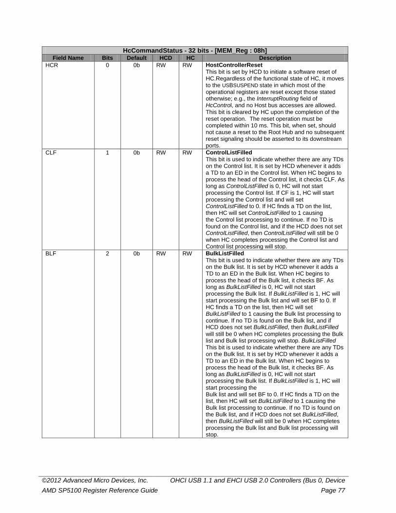
©2012 Advanced Micro Devices, Inc. OHCI USB 1.1 and EHCI USB 2.0 Controllers (Bus 0, Device AMD SP5100 Register Reference Guide Page 77
HcCommandStatus - 32 bits - [MEM_Reg : 08h] Field Name Bits Default HCD HC Description
HCR 0 0b RW RW HostControllerReset This bit is set by HCD to initiate a software reset of HC.Regardless of the functional state of HC, it moves to the USBSUSPEND state in which most of the operational registers are reset except those stated otherwise; e.g., the InterruptRouting field of HcControl, and no Host bus accesses are allowed. This bit is cleared by HC upon the completion of the reset operation. The reset operation must be completed within 10 ms. This bit, when set, should not cause a reset to the Root Hub and no subsequent reset signaling should be asserted to its downstream ports.
CLF 1 0b RW RW ControlListFilled This bit is used to indicate whether there are any TDs on the Control list. It is set by HCD whenever it adds a TD to an ED in the Control list. When HC begins to process the head of the Control list, it checks CLF. As long as ControlListFilled is 0, HC will not start processing the Control list. If CF is 1, HC will start processing the Control list and will set ControlListFilled to 0. If HC finds a TD on the list, then HC will set ControlListFilled to 1 causing the Control list processing to continue. If no TD is found on the Control list, and if the HCD does not set ControlListFilled, then ControlListFilled will still be 0 when HC completes processing the Control list and Control list processing will stop.
BLF 2 0b RW RW BulkListFilled This bit is used to indicate whether there are any TDs on the Bulk list. It is set by HCD whenever it adds a TD to an ED in the Bulk list. When HC begins to process the head of the Bulk list, it checks BF. As long as BulkListFilled is 0, HC will not start processing the Bulk list. If BulkListFilled is 1, HC will start processing the Bulk list and will set BF to 0. If HC finds a TD on the list, then HC will set BulkListFilled to 1 causing the Bulk list processing to continue. If no TD is found on the Bulk list, and if HCD does not set BulkListFilled, then BulkListFilled will still be 0 when HC completes processing the Bulk list and Bulk list processing will stop. BulkListFilled This bit is used to indicate whether there are any TDs on the Bulk list. It is set by HCD whenever it adds a TD to an ED in the Bulk list. When HC begins to process the head of the Bulk list, it checks BF. As long as BulkListFilled is 0, HC will not start processing the Bulk list. If BulkListFilled is 1, HC will start processing the Bulk list and will set BF to 0. If HC finds a TD on the list, then HC will set BulkListFilled to 1 causing the Bulk list processing to continue. If no TD is found on the Bulk list, and if HCD does not set BulkListFilled, then BulkListFilled will still be 0 when HC completes processing the Bulk list and Bulk list processing will stop.
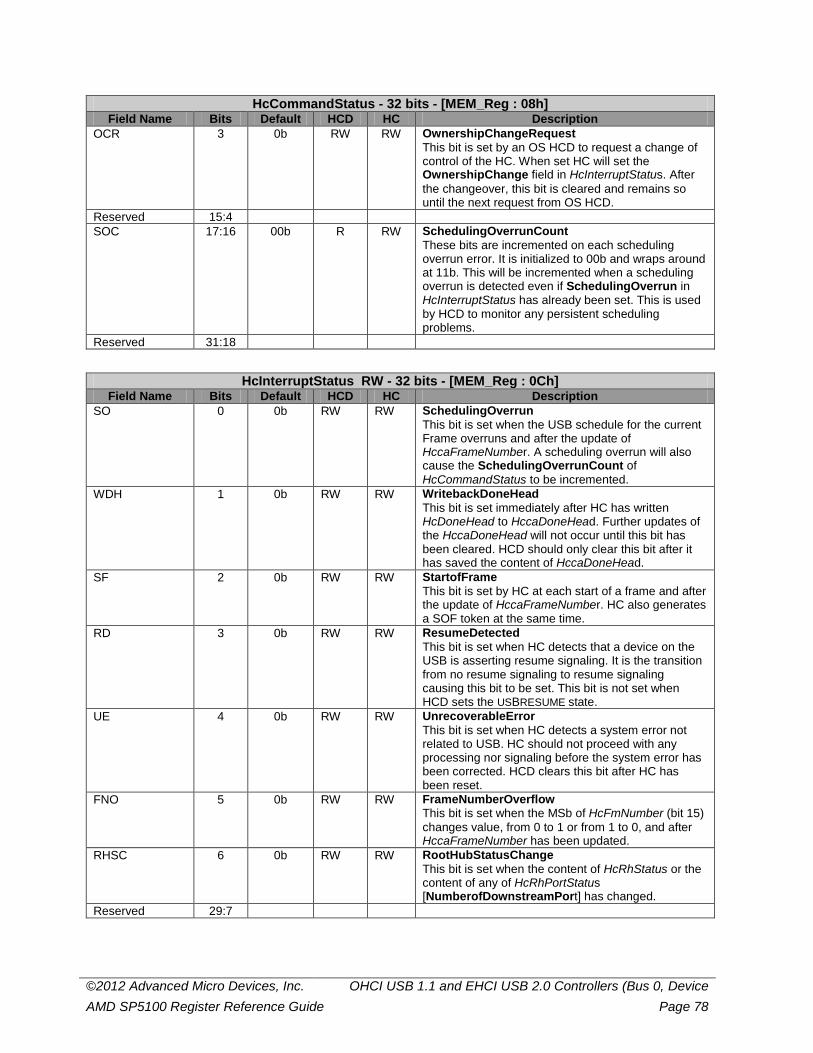
©2012 Advanced Micro Devices, Inc. OHCI USB 1.1 and EHCI USB 2.0 Controllers (Bus 0, Device AMD SP5100 Register Reference Guide Page 78
HcCommandStatus - 32 bits - [MEM_Reg : 08h] Field Name Bits Default HCD HC Description
OCR 3 0b RW RW OwnershipChangeRequest This bit is set by an OS HCD to request a change of control of the HC. When set HC will set the OwnershipChange field in HcInterruptStatus. After the changeover, this bit is cleared and remains so until the next request from OS HCD.
Reserved 15:4 SOC 17:16 00b R RW SchedulingOverrunCount
These bits are incremented on each scheduling overrun error. It is initialized to 00b and wraps around at 11b. This will be incremented when a scheduling overrun is detected even if SchedulingOverrun in HcInterruptStatus has already been set. This is used by HCD to monitor any persistent scheduling problems.
Reserved 31:18
HcInterruptStatus RW - 32 bits - [MEM_Reg : 0Ch] Field Name Bits Default HCD HC Description
SO 0 0b RW RW SchedulingOverrun This bit is set when the USB schedule for the current Frame overruns and after the update of HccaFrameNumber. A scheduling overrun will also cause the SchedulingOverrunCount of HcCommandStatus to be incremented.
WDH 1 0b RW RW WritebackDoneHead This bit is set immediately after HC has written HcDoneHead to HccaDoneHead. Further updates of the HccaDoneHead will not occur until this bit has been cleared. HCD should only clear this bit after it has saved the content of HccaDoneHead.
SF 2 0b RW RW StartofFrame This bit is set by HC at each start of a frame and after the update of HccaFrameNumber. HC also generates a SOF token at the same time.
RD 3 0b RW RW ResumeDetected This bit is set when HC detects that a device on the USB is asserting resume signaling. It is the transition from no resume signaling to resume signaling causing this bit to be set. This bit is not set when HCD sets the USBRESUME state.
UE 4 0b RW RW UnrecoverableError This bit is set when HC detects a system error not related to USB. HC should not proceed with any processing nor signaling before the system error has been corrected. HCD clears this bit after HC has been reset.
FNO 5 0b RW RW FrameNumberOverflow This bit is set when the MSb of HcFmNumber (bit 15) changes value, from 0 to 1 or from 1 to 0, and after HccaFrameNumber has been updated.
RHSC 6 0b RW RW RootHubStatusChange This bit is set when the content of HcRhStatus or the content of any of HcRhPortStatus [NumberofDownstreamPort] has changed.
Reserved 29:7
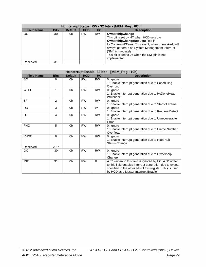
©2012 Advanced Micro Devices, Inc. OHCI USB 1.1 and EHCI USB 2.0 Controllers (Bus 0, Device AMD SP5100 Register Reference Guide Page 79
HcInterruptStatus RW - 32 bits - [MEM_Reg : 0Ch] Field Name Bits Default HCD HC Description
OC 30 0b RW RW OwnershipChange This bit is set by HC when HCD sets the OwnershipChangeRequest field in HcCommandStatus. This event, when unmasked, will always generate an System Management Interrupt (SMI) immediately. This bit is tied to 0b when the SMI pin is not implemented.
Reserved 31
HcInterruptEnable- 32 bits - [MEM_Reg : 10h] Field Name Bits Default HCD HC Description
SO 0 0b RW RW 0: Ignore 1: Enable interrupt generation due to Scheduling Overrun.
WDH 1 0b RW RW 0: Ignore 1: Enable interrupt generation due to HcDoneHead Writeback.
SF 2 0b RW RW 0: Ignore 1: Enable interrupt generation due to Start of Frame.
RD 3 0b RW W 0: Ignore 1: Enable interrupt generation due to Resume Detect.
UE 4 0b RW RW 0: Ignore 1: Enable interrupt generation due to Unrecoverable Error.
FNO 5 0b RW RW 0: Ignore 1: Enable interrupt generation due to Frame Number Overflow.
RHSC 6 0b RW RW 0: Ignore 1: Enable interrupt generation due to Root Hub Status Change.
Reserved 29:7 OC 30 0b RW RW 0: Ignore
1: Enable interrupt generation due to Ownership Change.
MIE 31 0b RW R A ‘0’ written to this field is ignored by HC. A '1' written to this field enables interrupt generation due to events specified in the other bits of this register. This is used by HCD as a Master Interrupt Enable.
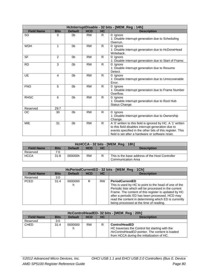
©2012 Advanced Micro Devices, Inc. OHCI USB 1.1 and EHCI USB 2.0 Controllers (Bus 0, Device AMD SP5100 Register Reference Guide Page 80
HcInterruptDisable - 32 bits - [MEM_Reg : 14h] Field Name Bits Default HCD HC Description
SO 0 0b RW R 0: Ignore 1: Disable interrupt generation due to Scheduling Overrun.
WDH 1 0b RW R 0: Ignore 1: Disable interrupt generation due to HcDoneHead Writeback.
SF 2 0b RW R 0: Ignore 1: Disable interrupt generation due to Start of Frame.
RD 3 0b RW R 0: Ignore 1: Disable interrupt generation due to Resume Detect.
UE 4 0b RW R 0: Ignore 1: Disable interrupt generation due to Unrecoverable Error.
FNO 5 0b RW R 0: Ignore 1: Disable interrupt generation due to Frame Number Overflow.
RHSC 6 0b RW R 0: Ignore 1: Disable interrupt generation due to Root Hub Status Change.
Reserved 29:7 OC 30 0b RW R 0: Ignore
1: Disable interrupt generation due to Ownership Change.
MIE 31 0b RW R A '0' written to this field is ignored by HC. A '1' written to this field disables interrupt generation due to events specified in the other bits of this register. This field is set after a hardware or software reset.
HcHCCA - 32 bits - [MEM_Reg : 18h] Field Name Bits Default HCD HC Description
Reserved 7:0 HCCA 31:8 000000h RW R This is the base address of the Host Controller
Communication Area
HcPeriodCurrentED - 32 bits - [MEM_Reg : 1Ch] Field Name Bits Default HCD HC Description
Reserved 3:0 PCED 31:4 0000000
h R RW PeriodCurrentED
This is used by HC to point to the head of one of the Periodic lists which will be processed in the current Frame. The content of this register is updated by HC after a periodic ED has been processed. HCD may read the content in determining which ED is currently being processed at the time of reading.
HcControlHeadED- 32 bits - [MEM_Reg : 20h] Field Name Bits Default HCD HC Description
Reserved 3:0 CHED 31:4 0000000
h RW R ControlHeadED
HC traverses the Control list starting with the HcControlHeadED pointer. The content is loaded from HCCA during the initialization of HC.
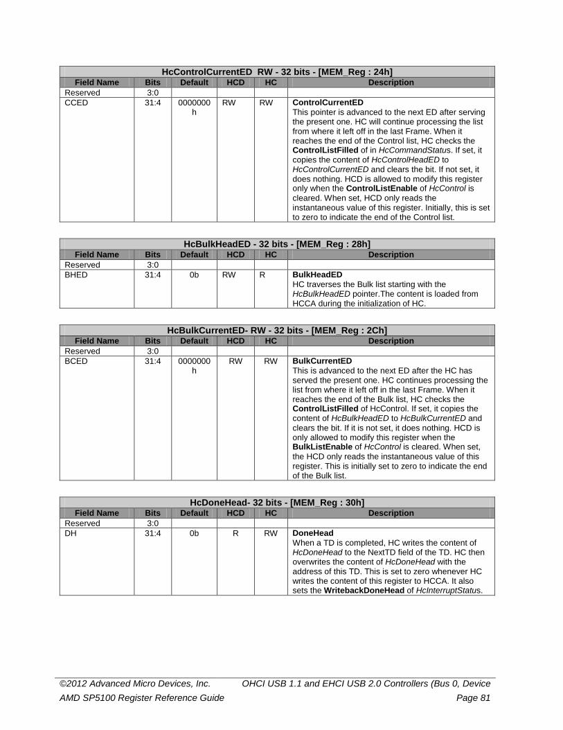
©2012 Advanced Micro Devices, Inc. OHCI USB 1.1 and EHCI USB 2.0 Controllers (Bus 0, Device AMD SP5100 Register Reference Guide Page 81
HcControlCurrentED RW - 32 bits - [MEM_Reg : 24h] Field Name Bits Default HCD HC Description
Reserved 3:0 CCED 31:4 0000000
h RW RW ControlCurrentED
This pointer is advanced to the next ED after serving the present one. HC will continue processing the list from where it left off in the last Frame. When it reaches the end of the Control list, HC checks the ControlListFilled of in HcCommandStatus. If set, it copies the content of HcControlHeadED to HcControlCurrentED and clears the bit. If not set, it does nothing. HCD is allowed to modify this register only when the ControlListEnable of HcControl is cleared. When set, HCD only reads the instantaneous value of this register. Initially, this is set to zero to indicate the end of the Control list.
HcBulkHeadED - 32 bits - [MEM_Reg : 28h] Field Name Bits Default HCD HC Description
Reserved 3:0 BHED 31:4 0b RW R BulkHeadED
HC traverses the Bulk list starting with the HcBulkHeadED pointer.The content is loaded from HCCA during the initialization of HC.
HcBulkCurrentED- RW - 32 bits - [MEM_Reg : 2Ch] Field Name Bits Default HCD HC Description
Reserved 3:0 BCED 31:4 0000000
h RW RW BulkCurrentED
This is advanced to the next ED after the HC has served the present one. HC continues processing the list from where it left off in the last Frame. When it reaches the end of the Bulk list, HC checks the ControlListFilled of HcControl. If set, it copies the content of HcBulkHeadED to HcBulkCurrentED and clears the bit. If it is not set, it does nothing. HCD is only allowed to modify this register when the BulkListEnable of HcControl is cleared. When set, the HCD only reads the instantaneous value of this register. This is initially set to zero to indicate the end of the Bulk list.
HcDoneHead- 32 bits - [MEM_Reg : 30h] Field Name Bits Default HCD HC Description
Reserved 3:0 DH 31:4 0b R RW DoneHead
When a TD is completed, HC writes the content of HcDoneHead to the NextTD field of the TD. HC then overwrites the content of HcDoneHead with the address of this TD. This is set to zero whenever HC writes the content of this register to HCCA. It also sets the WritebackDoneHead of HcInterruptStatus.
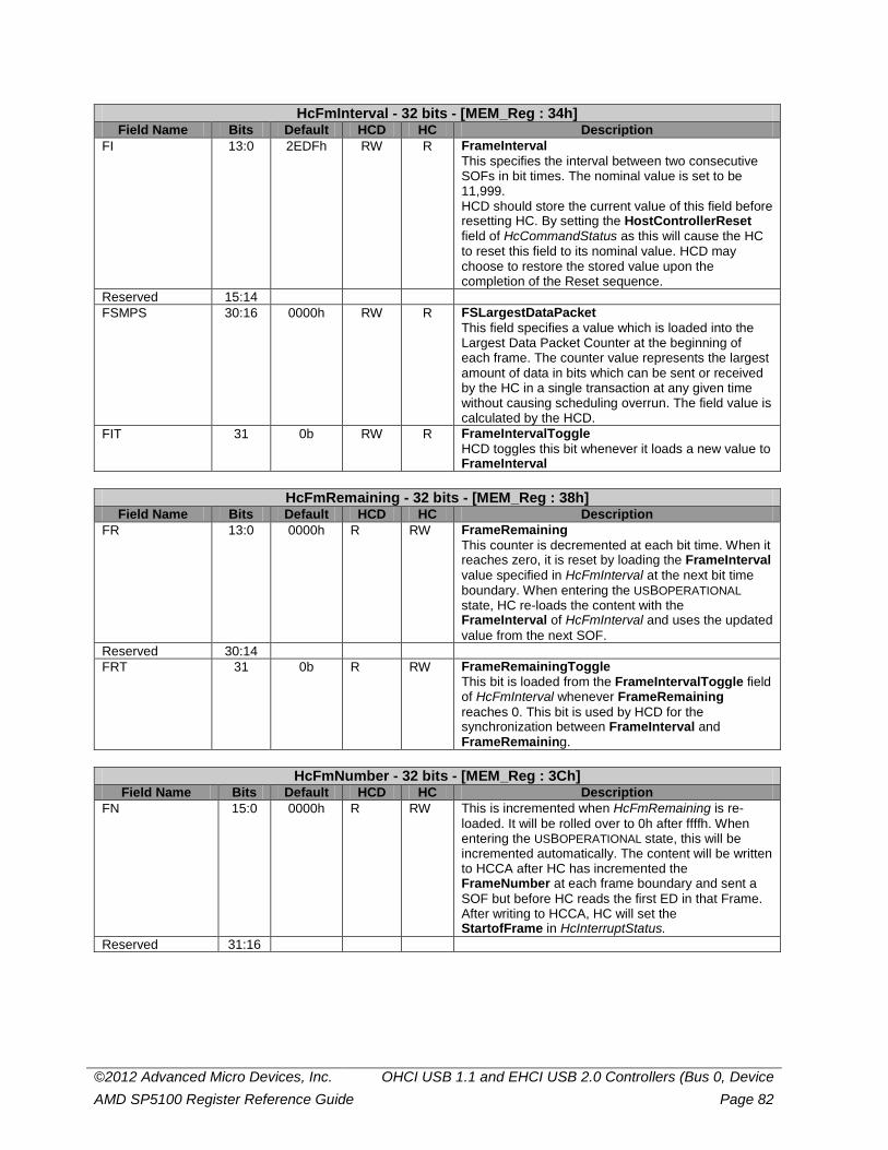
©2012 Advanced Micro Devices, Inc. OHCI USB 1.1 and EHCI USB 2.0 Controllers (Bus 0, Device AMD SP5100 Register Reference Guide Page 82
HcFmInterval - 32 bits - [MEM_Reg : 34h] Field Name Bits Default HCD HC Description
FI 13:0 2EDFh RW R FrameInterval This specifies the interval between two consecutive SOFs in bit times. The nominal value is set to be 11,999. HCD should store the current value of this field before resetting HC. By setting the HostControllerReset field of HcCommandStatus as this will cause the HC to reset this field to its nominal value. HCD may choose to restore the stored value upon the completion of the Reset sequence.
Reserved 15:14 FSMPS 30:16 0000h RW R FSLargestDataPacket
This field specifies a value which is loaded into the Largest Data Packet Counter at the beginning of each frame. The counter value represents the largest amount of data in bits which can be sent or received by the HC in a single transaction at any given time without causing scheduling overrun. The field value is calculated by the HCD.
FIT 31 0b RW R FrameIntervalToggle HCD toggles this bit whenever it loads a new value to FrameInterval
HcFmRemaining - 32 bits - [MEM_Reg : 38h]
Field Name Bits Default HCD HC Description FR 13:0 0000h R RW FrameRemaining
This counter is decremented at each bit time. When it reaches zero, it is reset by loading the FrameInterval value specified in HcFmInterval at the next bit time boundary. When entering the USBOPERATIONAL state, HC re-loads the content with the FrameInterval of HcFmInterval and uses the updated value from the next SOF.
Reserved 30:14 FRT 31 0b R RW FrameRemainingToggle
This bit is loaded from the FrameIntervalToggle field of HcFmInterval whenever FrameRemaining reaches 0. This bit is used by HCD for the synchronization between FrameInterval and FrameRemaining.
HcFmNumber - 32 bits - [MEM_Reg : 3Ch]
Field Name Bits Default HCD HC Description FN 15:0 0000h R RW This is incremented when HcFmRemaining is re-
loaded. It will be rolled over to 0h after ffffh. When entering the USBOPERATIONAL state, this will be incremented automatically. The content will be written to HCCA after HC has incremented the FrameNumber at each frame boundary and sent a SOF but before HC reads the first ED in that Frame. After writing to HCCA, HC will set the StartofFrame in HcInterruptStatus.
Reserved 31:16
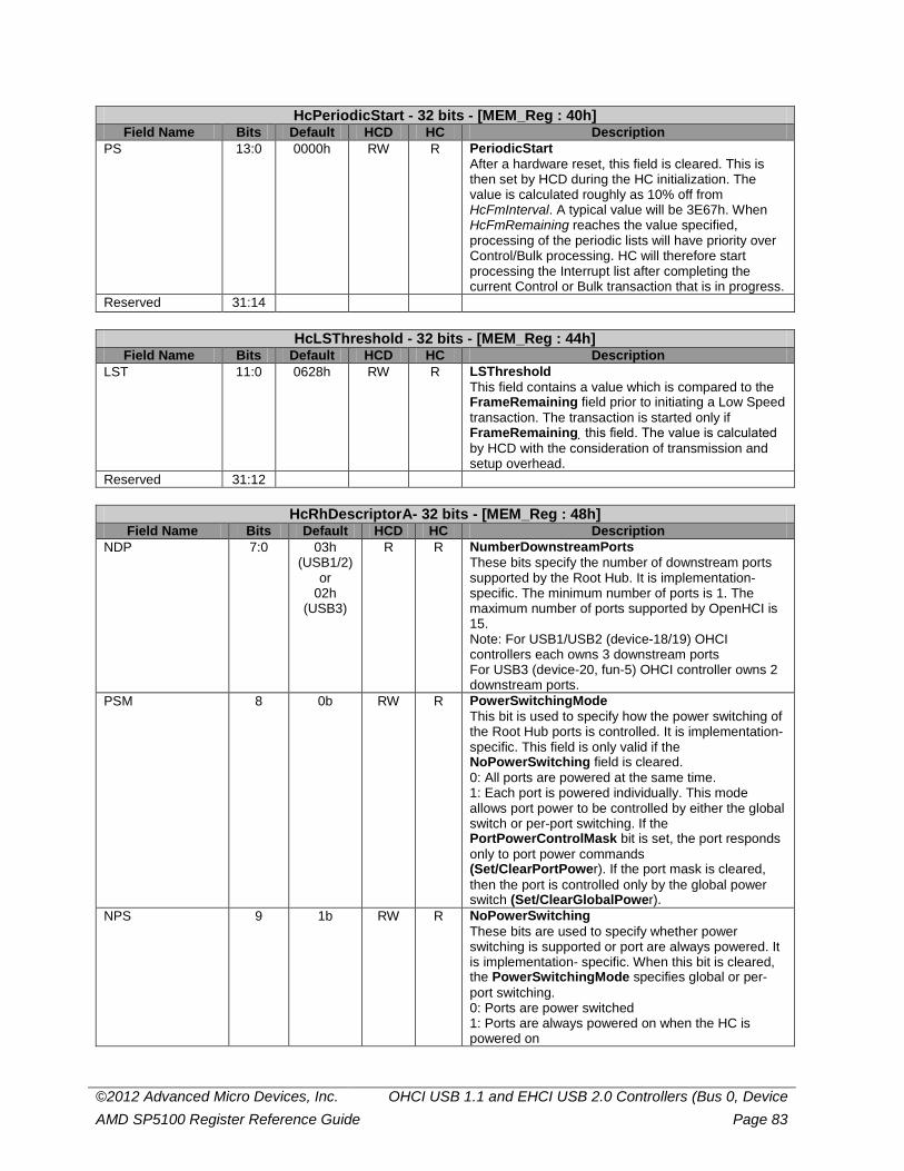
©2012 Advanced Micro Devices, Inc. OHCI USB 1.1 and EHCI USB 2.0 Controllers (Bus 0, Device AMD SP5100 Register Reference Guide Page 83
HcPeriodicStart - 32 bits - [MEM_Reg : 40h] Field Name Bits Default HCD HC Description
PS 13:0 0000h RW R PeriodicStart After a hardware reset, this field is cleared. This is then set by HCD during the HC initialization. The value is calculated roughly as 10% off from HcFmInterval. A typical value will be 3E67h. When HcFmRemaining reaches the value specified, processing of the periodic lists will have priority over Control/Bulk processing. HC will therefore start processing the Interrupt list after completing the current Control or Bulk transaction that is in progress.
Reserved 31:14
HcLSThreshold - 32 bits - [MEM_Reg : 44h] Field Name Bits Default HCD HC Description
LST 11:0 0628h RW R LSThreshold This field contains a value which is compared to the FrameRemaining field prior to initiating a Low Speed transaction. The transaction is started only if FrameRemaining this field. The value is calculated by HCD with the consideration of transmission and setup overhead.
Reserved 31:12
HcRhDescriptorA- 32 bits - [MEM_Reg : 48h] Field Name Bits Default HCD HC Description
NDP 7:0 03h (USB1/2)
or 02h
(USB3)
R R NumberDownstreamPorts These bits specify the number of downstream ports supported by the Root Hub. It is implementation-specific. The minimum number of ports is 1. The maximum number of ports supported by OpenHCI is 15. Note: For USB1/USB2 (device-18/19) OHCI controllers each owns 3 downstream ports For USB3 (device-20, fun-5) OHCI controller owns 2 downstream ports.
PSM 8 0b RW R PowerSwitchingMode This bit is used to specify how the power switching of the Root Hub ports is controlled. It is implementation-specific. This field is only valid if the NoPowerSwitching field is cleared. 0: All ports are powered at the same time. 1: Each port is powered individually. This mode allows port power to be controlled by either the global switch or per-port switching. If the PortPowerControlMask bit is set, the port responds only to port power commands (Set/ClearPortPower). If the port mask is cleared, then the port is controlled only by the global power switch (Set/ClearGlobalPower).
NPS 9 1b RW R NoPowerSwitching These bits are used to specify whether power switching is supported or port are always powered. It is implementation- specific. When this bit is cleared, the PowerSwitchingMode specifies global or per-port switching. 0: Ports are power switched 1: Ports are always powered on when the HC is powered on
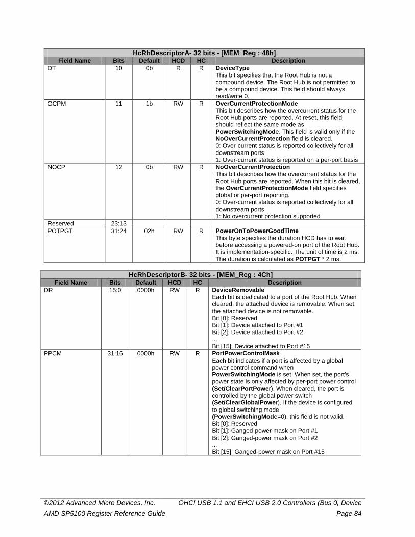
©2012 Advanced Micro Devices, Inc. OHCI USB 1.1 and EHCI USB 2.0 Controllers (Bus 0, Device AMD SP5100 Register Reference Guide Page 84
HcRhDescriptorA- 32 bits - [MEM_Reg : 48h] Field Name Bits Default HCD HC Description
DT 10 0b R R DeviceType This bit specifies that the Root Hub is not a compound device. The Root Hub is not permitted to be a compound device. This field should always read/write 0.
OCPM 11 1b RW R OverCurrentProtectionMode This bit describes how the overcurrent status for the Root Hub ports are reported. At reset, this field should reflect the same mode as PowerSwitchingMode. This field is valid only if the NoOverCurrentProtection field is cleared. 0: Over-current status is reported collectively for all downstream ports 1: Over-current status is reported on a per-port basis
NOCP 12 0b RW R NoOverCurrentProtection This bit describes how the overcurrent status for the Root Hub ports are reported. When this bit is cleared, the OverCurrentProtectionMode field specifies global or per-port reporting. 0: Over-current status is reported collectively for all downstream ports 1: No overcurrent protection supported
Reserved 23:13 POTPGT 31:24 02h RW R PowerOnToPowerGoodTime
This byte specifies the duration HCD has to wait before accessing a powered-on port of the Root Hub. It is implementation-specific. The unit of time is 2 ms. The duration is calculated as POTPGT * 2 ms.
HcRhDescriptorB- 32 bits - [MEM_Reg : 4Ch]
Field Name Bits Default HCD HC Description DR 15:0 0000h RW R DeviceRemovable
Each bit is dedicated to a port of the Root Hub. When cleared, the attached device is removable. When set, the attached device is not removable. Bit [0]: Reserved Bit [1]: Device attached to Port #1 Bit [2]: Device attached to Port #2 ... Bit [15]: Device attached to Port #15
PPCM 31:16 0000h RW R PortPowerControlMask Each bit indicates if a port is affected by a global power control command when PowerSwitchingMode is set. When set, the port's power state is only affected by per-port power control (Set/ClearPortPower). When cleared, the port is controlled by the global power switch (Set/ClearGlobalPower). If the device is configured to global switching mode (PowerSwitchingMode=0), this field is not valid. Bit [0]: Reserved Bit [1]: Ganged-power mask on Port #1 Bit [2]: Ganged-power mask on Port #2 ... Bit [15]: Ganged-power mask on Port #15
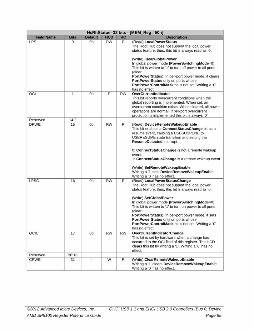
©2012 Advanced Micro Devices, Inc. OHCI USB 1.1 and EHCI USB 2.0 Controllers (Bus 0, Device AMD SP5100 Register Reference Guide Page 85
HcRhStatus- 32 bits - [MEM_Reg : 50h] Field Name Bits Default HCD HC Description
LPS 0 0b RW R (Read) LocalPowerStatus The Root Hub does not support the local power status feature; thus, this bit is always read as ‘0’. (Write) ClearGlobalPower In global power mode (PowerSwitchingMode=0), This bit is written to ‘1’ to turn off power to all ports (clear PortPowerStatus). In per-port power mode, it clears PortPowerStatus only on ports whose PortPowerControlMask bit is not set. Writing a ‘0’ has no effect.
OCI 1 0b R RW OverCurrentIndicator This bit reports overcurrent conditions when the global reporting is implemented. When set, an overcurrent condition exists. When cleared, all power operations are normal. If per-port overcurrent protection is implemented this bit is always ‘0’
Reserved 14:2 DRWE 15 0b RW R (Read) DeviceRemoteWakeupEnable
This bit enables a ConnectStatusChange bit as a resume event, causing a USBSUSPEND to USBRESUME state transition and setting the ResumeDetected interrupt. 0: ConnectStatusChange is not a remote wakeup event. 1: ConnectStatusChange is a remote wakeup event. (Write) SetRemoteWakeupEnable Writing a '1' sets DeviceRemoveWakeupEnable. Writing a '0' has no effect.
LPSC 16 0b RW R (Read) LocalPowerStatusChange The Root Hub does not support the local power status feature; thus, this bit is always read as ‘0’. (Write) SetGlobalPower In global power mode (PowerSwitchingMode=0), This bit is written to ‘1’ to turn on power to all ports (clear PortPowerStatus). In per-port power mode, it sets PortPowerStatus only on ports whose PortPowerControlMask bit is not set. Writing a ‘0’ has no effect.
OCIC 17 0b RW RW OverCurrentIndicatorChange This bit is set by hardware when a change has occurred to the OCI field of this register. The HCD clears this bit by writing a ‘1’. Writing a ‘0’ has no effect.
Reserved 30:18 CRWE 31 - W R (Write) ClearRemoteWakeupEnable
Writing a '1' clears DeviceRemoveWakeupEnable. Writing a '0' has no effect.
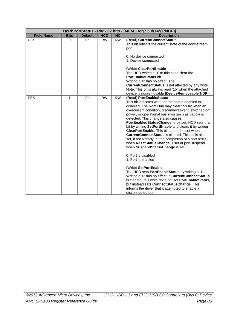
©2012 Advanced Micro Devices, Inc. OHCI USB 1.1 and EHCI USB 2.0 Controllers (Bus 0, Device AMD SP5100 Register Reference Guide Page 86
HcRhPortStatus - RW - 32 bits - [MEM_Reg : 50h+4*(1:NDP)] Field Name Bits Default HCD HC Description
CCS 0 0b RW RW (Read) CurrentConnectStatus This bit reflects the current state of the downstream port. 0: No device connected 1: Device connected (Write) ClearPortEnable The HCD writes a ‘1’ to this bit to clear the PortEnableStatus bit. Writing a ‘0’ has no effect. The CurrentConnectStatus is not affected by any write. Note: This bit is always read ‘1b’ when the attached device is nonremovable (DeviceRemoveable[NDP]).
PES 1 0b RW RW (Read) PortEnableStatus This bit indicates whether the port is enabled or disabled. The Root Hub may clear this bit when an overcurrent condition, disconnect event, switched-off power, or operational bus error such as babble is detected. This change also causes PortEnabledStatusChange to be set. HCD sets this bit by writing SetPortEnable and clears it by writing ClearPortEnable. This bit cannot be set when CurrentConnectStatus is cleared. This bit is also set, if not already, at the completion of a port reset when ResetStatusChange is set or port suspend when SuspendStatusChange is set. 0: Port is disabled 1: Port is enabled (Write) SetPortEnable The HCD sets PortEnableStatus by writing a ‘1’. Writing a ‘0’ has no effect. If CurrentConnectStatus is cleared, this write does not set PortEnableStatus, but instead sets ConnectStatusChange. This informs the driver that it attempted to enable a disconnected port.
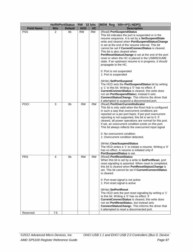
©2012 Advanced Micro Devices, Inc. OHCI USB 1.1 and EHCI USB 2.0 Controllers (Bus 0, Device AMD SP5100 Register Reference Guide Page 87
HcRhPortStatus - RW - 32 bits - [MEM_Reg : 50h+4*(1:NDP)] Field Name Bits Default HCD HC Description
PSS 2 0b RW RW (Read) PortSuspendStatus This bit indicates the port is suspended or in the resume sequence. It is set by a SetSuspendState write and cleared when PortSuspendStatusChange is set at the end of the resume interval. This bit cannot be set if CurrentConnectStatus is cleared. This bit is also cleared when PortResetStatusChange is set at the end of the port reset or when the HC is placed in the USBRESUME state. If an upstream resume is in progress, it should propagate to the HC. 0: Port is not suspended 1: Port is suspended (Write) SetPortSuspend The HCD sets the PortSuspendStatus bit by writing a ‘1’ to this bit. Writing a ‘0’ has no effect. If CurrentConnectStatus is cleared, this write does not set PortSuspendStatus; instead it sets ConnectStatusChange. This informs the driver that it attempted to suspend a disconnected port.
POCI 3 0b RW RW (Read) PortOverCurrentIndicator This bit is only valid when the Root Hub is configured in such a way that overcurrent conditions are reported on a per-port basis. If per-port overcurrent reporting is not supported, this bit is set to 0. If cleared, all power operations are normal for this port. If set, an overcurrent condition exists on this port. This bit always reflects the overcurrent input signal 0: No overcurrent condition. 1: Overcurrent condition detected. (Write) ClearSuspendStatus The HCD writes a ‘1’ to initiate a resume. Writing a ‘0’ has no effect. A resume is initiated only if PortSuspendStatus is set.
PRS 4 0b RW RW (Read) PortResetStatus When this bit is set by a write to SetPortReset, port reset signaling is asserted. When reset is completed, this bit is cleared when PortResetStatusChange is set. This bit cannot be set if CurrentConnectStatus is cleared. 0: Port reset signal is not active 1: Port reset signal is active (Write) SetPortReset The HCD sets the port reset signaling by writing a ‘1’ to this bit. Writing a ‘0’ has no effect. If CurrentConnectStatus is cleared, this write does not set PortResetStatus, but instead sets ConnectStatusChange. This informs the driver that it attempted to reset a disconnected port.
Reserved 7:5
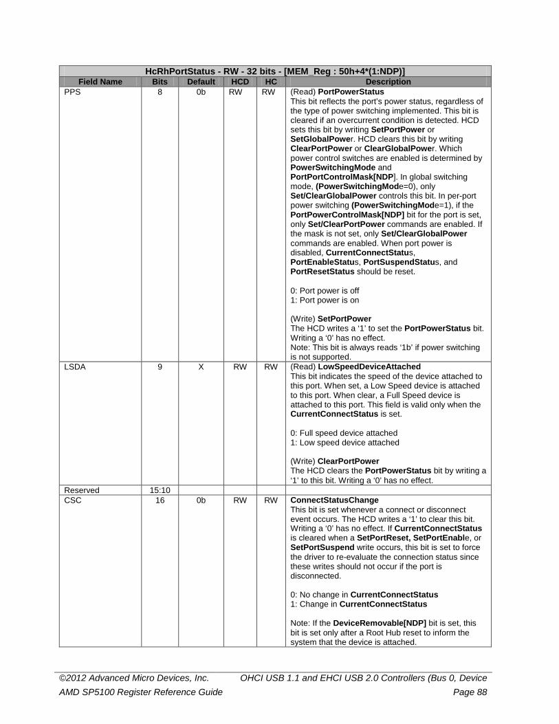
©2012 Advanced Micro Devices, Inc. OHCI USB 1.1 and EHCI USB 2.0 Controllers (Bus 0, Device AMD SP5100 Register Reference Guide Page 88
HcRhPortStatus - RW - 32 bits - [MEM_Reg : 50h+4*(1:NDP)] Field Name Bits Default HCD HC Description
PPS 8 0b RW RW (Read) PortPowerStatus This bit reflects the port’s power status, regardless of the type of power switching implemented. This bit is cleared if an overcurrent condition is detected. HCD sets this bit by writing SetPortPower or SetGlobalPower. HCD clears this bit by writing ClearPortPower or ClearGlobalPower. Which power control switches are enabled is determined by PowerSwitchingMode and PortPortControlMask[NDP]. In global switching mode, (PowerSwitchingMode=0), only Set/ClearGlobalPower controls this bit. In per-port power switching (PowerSwitchingMode=1), if the PortPowerControlMask[NDP] bit for the port is set, only Set/ClearPortPower commands are enabled. If the mask is not set, only Set/ClearGlobalPower commands are enabled. When port power is disabled, CurrentConnectStatus, PortEnableStatus, PortSuspendStatus, and PortResetStatus should be reset. 0: Port power is off 1: Port power is on (Write) SetPortPower The HCD writes a ‘1’ to set the PortPowerStatus bit. Writing a ‘0’ has no effect. Note: This bit is always reads ‘1b’ if power switching is not supported.
LSDA 9 X RW RW (Read) LowSpeedDeviceAttached This bit indicates the speed of the device attached to this port. When set, a Low Speed device is attached to this port. When clear, a Full Speed device is attached to this port. This field is valid only when the CurrentConnectStatus is set. 0: Full speed device attached 1: Low speed device attached (Write) ClearPortPower The HCD clears the PortPowerStatus bit by writing a ‘1’ to this bit. Writing a ‘0’ has no effect.
Reserved 15:10 CSC 16 0b RW RW ConnectStatusChange
This bit is set whenever a connect or disconnect event occurs. The HCD writes a ‘1’ to clear this bit. Writing a ‘0’ has no effect. If CurrentConnectStatus is cleared when a SetPortReset, SetPortEnable, or SetPortSuspend write occurs, this bit is set to force the driver to re-evaluate the connection status since these writes should not occur if the port is disconnected. 0: No change in CurrentConnectStatus 1: Change in CurrentConnectStatus Note: If the DeviceRemovable[NDP] bit is set, this bit is set only after a Root Hub reset to inform the system that the device is attached.
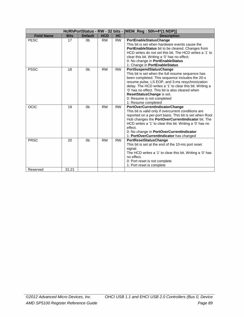
©2012 Advanced Micro Devices, Inc. OHCI USB 1.1 and EHCI USB 2.0 Controllers (Bus 0, Device AMD SP5100 Register Reference Guide Page 89
HcRhPortStatus - RW - 32 bits - [MEM_Reg : 50h+4*(1:NDP)] Field Name Bits Default HCD HC Description
PESC 17 0b RW RW PortEnableStatusChange This bit is set when hardware events cause the PortEnableStatus bit to be cleared. Changes from HCD writes do not set this bit. The HCD writes a ‘1’ to clear this bit. Writing a ‘0’ has no effect. 0: No change in PortEnableStatus 1: Change in PortEnableStatus
PSSC 18 0b RW RW PortSuspendStatusChange This bit is set when the full resume sequence has been completed. This sequence includes the 20-s resume pulse, LS EOP, and 3-ms resychronization delay. The HCD writes a ‘1’ to clear this bit. Writing a ‘0’ has no effect. This bit is also cleared when ResetStatusChange is set. 0: Resume is not completed 1: Resume completed
OCIC 19 0b RW RW PortOverCurrentIndicatorChange This bit is valid only if overcurrent conditions are reported on a per-port basis. This bit is set when Root Hub changes the PortOverCurrentIndicator bit. The HCD writes a ‘1’ to clear this bit. Writing a ‘0’ has no effect. 0: No change in PortOverCurrentIndicator 1: PortOverCurrentIndicator has changed
PRSC 20 0b RW RW PortResetStatusChange This bit is set at the end of the 10-ms port reset signal. The HCD writes a ‘1’ to clear this bit. Writing a ‘0’ has no effect. 0: Port reset is not complete 1: Port reset is complete
Reserved 31:21
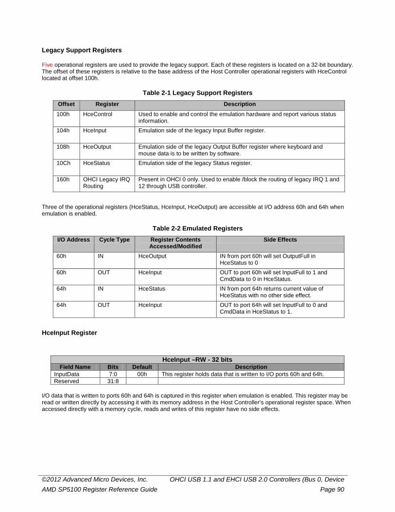
©2012 Advanced Micro Devices, Inc. OHCI USB 1.1 and EHCI USB 2.0 Controllers (Bus 0, Device AMD SP5100 Register Reference Guide Page 90
Legacy Support Registers Five operational registers are used to provide the legacy support. Each of these registers is located on a 32-bit boundary. The offset of these registers is relative to the base address of the Host Controller operational registers with HceControl located at offset 100h.
Table 2-1 Legacy Support Registers Offset Register Description
100h HceControl Used to enable and control the emulation hardware and report various status information.
104h HceInput Emulation side of the legacy Input Buffer register.
108h HceOutput Emulation side of the legacy Output Buffer register where keyboard and mouse data is to be written by software.
10Ch HceStatus Emulation side of the legacy Status register.
160h OHCI Legacy IRQ Routing
Present in OHCI 0 only. Used to enable /block the routing of legacy IRQ 1 and 12 through USB controller.
Three of the operational registers (HceStatus, HceInput, HceOutput) are accessible at I/O address 60h and 64h when emulation is enabled.
Table 2-2 Emulated Registers I/O Address Cycle Type Register Contents
Accessed/Modified Side Effects
60h IN HceOutput IN from port 60h will set OutputFull in HceStatus to 0
60h OUT HceInput OUT to port 60h will set InputFull to 1 and CmdData to 0 in HceStatus.
64h IN HceStatus IN from port 64h returns current value of HceStatus with no other side effect.
64h OUT HceInput OUT to port 64h will set InputFull to 0 and CmdData in HceStatus to 1.
HceInput Register
HceInput –RW - 32 bits Field Name Bits Default Description
InputData 7:0 00h This register holds data that is written to I/O ports 60h and 64h. Reserved 31:8
I/O data that is written to ports 60h and 64h is captured in this register when emulation is enabled. This register may be read or written directly by accessing it with its memory address in the Host Controller’s operational register space. When accessed directly with a memory cycle, reads and writes of this register have no side effects.
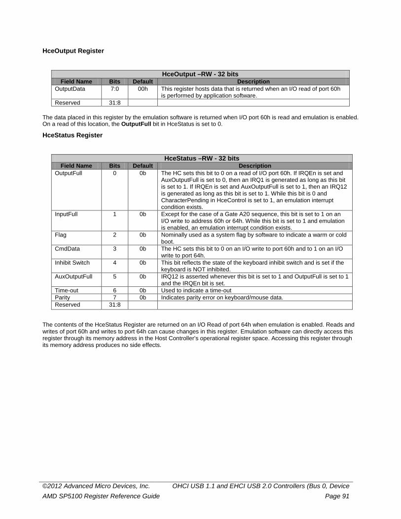
©2012 Advanced Micro Devices, Inc. OHCI USB 1.1 and EHCI USB 2.0 Controllers (Bus 0, Device AMD SP5100 Register Reference Guide Page 91
HceOutput Register
HceOutput –RW - 32 bits Field Name Bits Default Description
OutputData 7:0 00h This register hosts data that is returned when an I/O read of port 60h is performed by application software.
Reserved 31:8 The data placed in this register by the emulation software is returned when I/O port 60h is read and emulation is enabled. On a read of this location, the OutputFull bit in HceStatus is set to 0.
HceStatus Register
HceStatus –RW - 32 bits Field Name Bits Default Description
OutputFull 0 0b The HC sets this bit to 0 on a read of I/O port 60h. If IRQEn is set and AuxOutputFull is set to 0, then an IRQ1 is generated as long as this bit is set to 1. If IRQEn is set and AuxOutputFull is set to 1, then an IRQ12 is generated as long as this bit is set to 1. While this bit is 0 and CharacterPending in HceControl is set to 1, an emulation interrupt condition exists.
InputFull 1 0b Except for the case of a Gate A20 sequence, this bit is set to 1 on an I/O write to address 60h or 64h. While this bit is set to 1 and emulation is enabled, an emulation interrupt condition exists.
Flag 2 0b Nominally used as a system flag by software to indicate a warm or cold boot.
CmdData 3 0b The HC sets this bit to 0 on an I/O write to port 60h and to 1 on an I/O write to port 64h.
Inhibit Switch 4 0b This bit reflects the state of the keyboard inhibit switch and is set if the keyboard is NOT inhibited.
AuxOutputFull 5 0b IRQ12 is asserted whenever this bit is set to 1 and OutputFull is set to 1 and the IRQEn bit is set.
Time-out 6 0b Used to indicate a time-out Parity 7 0b Indicates parity error on keyboard/mouse data. Reserved 31:8
The contents of the HceStatus Register are returned on an I/O Read of port 64h when emulation is enabled. Reads and writes of port 60h and writes to port 64h can cause changes in this register. Emulation software can directly access this register through its memory address in the Host Controller’s operational register space. Accessing this register through its memory address produces no side effects.
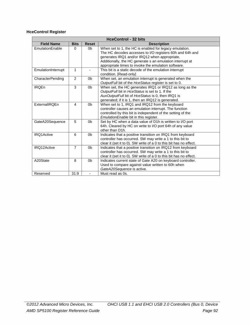
©2012 Advanced Micro Devices, Inc. OHCI USB 1.1 and EHCI USB 2.0 Controllers (Bus 0, Device AMD SP5100 Register Reference Guide Page 92
HceControl Register
HceControl - 32 bits Field Name Bits Reset Description
EmulationEnable 0 0b When set to 1, the HC is enabled for legacy emulation. The HC decodes accesses to I/O registers 60h and 64h and generates IRQ1 and/or IRQ12 when appropriate. Additionally, the HC generate s an emulation interrupt at appropriate times to invoke the emulation software.
EmulationInterrupt 1 - This bit is a static decode of the emulation interrupt condition. [Read-only]
CharacterPending 2 0b When set, an emulation interrupt is generated when the OutputFull bit of the HceStatus register is set to 0.
IRQEn 3 0b When set, the HC generates IRQ1 or IRQ12 as long as the OutputFull bit in HceStatus is set to 1. If the AuxOutputFull bit of HceStatus is 0, then IRQ1 is generated; if it is 1, then an IRQ12 is generated.
ExternalIRQEn 4 0b When set to 1, IRQ1 and IRQ12 from the keyboard controller causes an emulation interrupt. The function controlled by this bit is independent of the setting of the EmulationEnable bit in this register.
GateA20Sequence 5 0b Set by HC when a data value of D1h is written to I/O port 64h. Cleared by HC on write to I/O port 64h of any value other than D1h.
IRQ1Active 6 0b Indicates that a positive transition on IRQ1 from keyboard controller has occurred. SW may write a 1 to this bit to clear it (set it to 0). SW write of a 0 to this bit has no effect.
IRQ12Active 7 0b Indicates that a positive transition on IRQ12 from keyboard controller has occurred. SW may write a 1 to this bit to clear it (set it to 0). SW write of a 0 to this bit has no effect.
A20State 8 0b Indicates current state of Gate A20 on keyboard controller. Used to compare against value written to 60h when GateA20Sequence is active.
Reserved 31:9 - Must read as 0s.
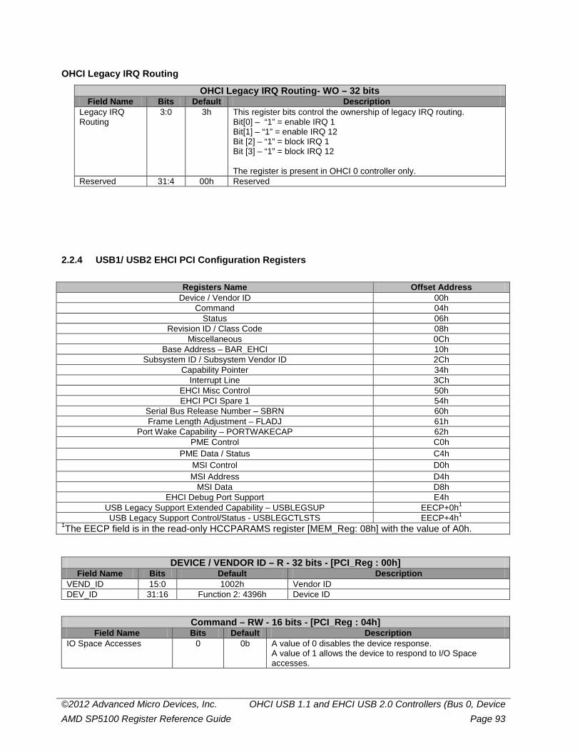
©2012 Advanced Micro Devices, Inc. OHCI USB 1.1 and EHCI USB 2.0 Controllers (Bus 0, Device AMD SP5100 Register Reference Guide Page 93
OHCI Legacy IRQ Routing
OHCI Legacy IRQ Routing- WO – 32 bits Field Name Bits Default Description
Legacy IRQ Routing
3:0 3h This register bits control the ownership of legacy IRQ routing. Bit[0] – “1” = enable IRQ 1 Bit[1] – “1” = enable IRQ 12 Bit [2] – “1” = block IRQ 1 Bit [3] – “1” = block IRQ 12 The register is present in OHCI 0 controller only.
Reserved 31:4 00h Reserved
2.2.4 USB1/ USB2 EHCI PCI Configuration Registers
Registers Name Offset Address
Device / Vendor ID 00h Command 04h
Status 06h Revision ID / Class Code 08h
Miscellaneous 0Ch Base Address – BAR_EHCI 10h
Subsystem ID / Subsystem Vendor ID 2Ch Capability Pointer 34h
Interrupt Line 3Ch EHCI Misc Control 50h EHCI PCI Spare 1 54h
Serial Bus Release Number – SBRN 60h Frame Length Adjustment – FLADJ 61h
Port Wake Capability – PORTWAKECAP 62h PME Control C0h
PME Data / Status C4h MSI Control D0h MSI Address D4h
MSI Data D8h EHCI Debug Port Support E4h
USB Legacy Support Extended Capability – USBLEGSUP EECP+0h1 USB Legacy Support Control/Status - USBLEGCTLSTS EECP+4h1
1The EECP field is in the read-only HCCPARAMS register [MEM_Reg: 08h] with the value of A0h.
DEVICE / VENDOR ID – R - 32 bits - [PCI_Reg : 00h] Field Name Bits Default Description
VEND_ID 15:0 1002h Vendor ID DEV_ID 31:16 Function 2: 4396h Device ID
Command – RW - 16 bits - [PCI_Reg : 04h] Field Name Bits Default Description
IO Space Accesses 0 0b A value of 0 disables the device response. A value of 1 allows the device to respond to I/O Space accesses.
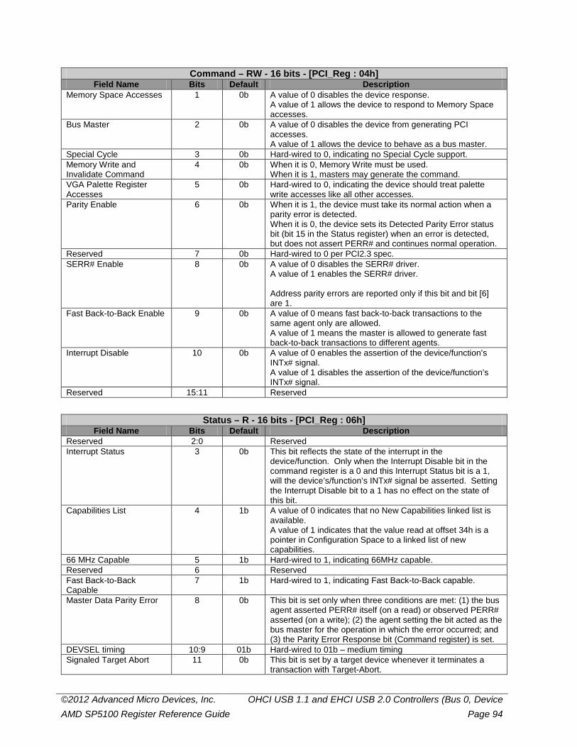
©2012 Advanced Micro Devices, Inc. OHCI USB 1.1 and EHCI USB 2.0 Controllers (Bus 0, Device AMD SP5100 Register Reference Guide Page 94
Command – RW - 16 bits - [PCI_Reg : 04h] Field Name Bits Default Description
Memory Space Accesses 1 0b A value of 0 disables the device response. A value of 1 allows the device to respond to Memory Space accesses.
Bus Master 2 0b A value of 0 disables the device from generating PCI accesses. A value of 1 allows the device to behave as a bus master.
Special Cycle 3 0b Hard-wired to 0, indicating no Special Cycle support. Memory Write and Invalidate Command
4 0b When it is 0, Memory Write must be used. When it is 1, masters may generate the command.
VGA Palette Register Accesses
5 0b Hard-wired to 0, indicating the device should treat palette write accesses like all other accesses.
Parity Enable 6 0b When it is 1, the device must take its normal action when a parity error is detected. When it is 0, the device sets its Detected Parity Error status bit (bit 15 in the Status register) when an error is detected, but does not assert PERR# and continues normal operation.
Reserved 7 0b Hard-wired to 0 per PCI2.3 spec. SERR# Enable 8 0b A value of 0 disables the SERR# driver.
A value of 1 enables the SERR# driver. Address parity errors are reported only if this bit and bit [6] are 1.
Fast Back-to-Back Enable 9 0b A value of 0 means fast back-to-back transactions to the same agent only are allowed. A value of 1 means the master is allowed to generate fast back-to-back transactions to different agents.
Interrupt Disable 10 0b A value of 0 enables the assertion of the device/function’s INTx# signal. A value of 1 disables the assertion of the device/function’s INTx# signal.
Reserved 15:11 Reserved
Status – R - 16 bits - [PCI_Reg : 06h] Field Name Bits Default Description
Reserved 2:0 Reserved Interrupt Status 3 0b This bit reflects the state of the interrupt in the
device/function. Only when the Interrupt Disable bit in the command register is a 0 and this Interrupt Status bit is a 1, will the device’s/function’s INTx# signal be asserted. Setting the Interrupt Disable bit to a 1 has no effect on the state of this bit.
Capabilities List 4 1b A value of 0 indicates that no New Capabilities linked list is available. A value of 1 indicates that the value read at offset 34h is a pointer in Configuration Space to a linked list of new capabilities.
66 MHz Capable 5 1b Hard-wired to 1, indicating 66MHz capable. Reserved 6 Reserved Fast Back-to-Back Capable
7 1b Hard-wired to 1, indicating Fast Back-to-Back capable.
Master Data Parity Error 8 0b This bit is set only when three conditions are met: (1) the bus agent asserted PERR# itself (on a read) or observed PERR# asserted (on a write); (2) the agent setting the bit acted as the bus master for the operation in which the error occurred; and (3) the Parity Error Response bit (Command register) is set.
DEVSEL timing 10:9 01b Hard-wired to 01b – medium timing Signaled Target Abort 11 0b This bit is set by a target device whenever it terminates a
transaction with Target-Abort.
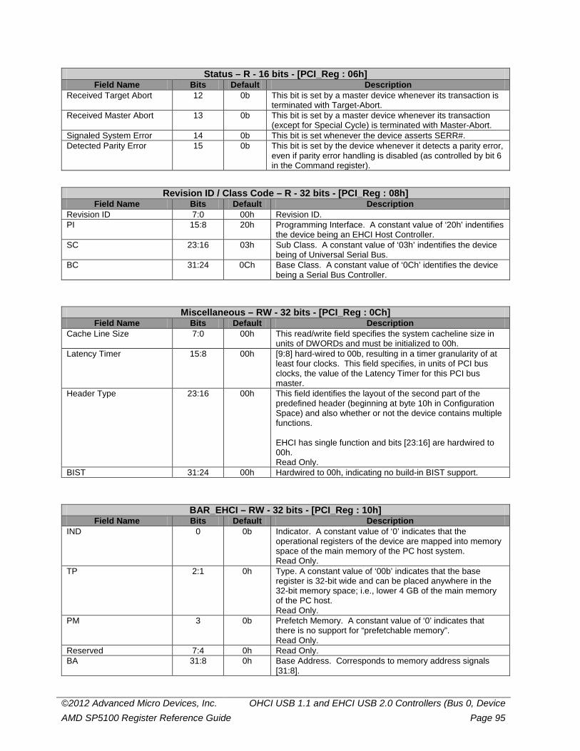
©2012 Advanced Micro Devices, Inc. OHCI USB 1.1 and EHCI USB 2.0 Controllers (Bus 0, Device AMD SP5100 Register Reference Guide Page 95
Status – R - 16 bits - [PCI_Reg : 06h] Field Name Bits Default Description
Received Target Abort 12 0b This bit is set by a master device whenever its transaction is terminated with Target-Abort.
Received Master Abort 13 0b This bit is set by a master device whenever its transaction (except for Special Cycle) is terminated with Master-Abort.
Signaled System Error 14 0b This bit is set whenever the device asserts SERR#. Detected Parity Error 15 0b This bit is set by the device whenever it detects a parity error,
even if parity error handling is disabled (as controlled by bit 6 in the Command register).
Revision ID / Class Code – R - 32 bits - [PCI_Reg : 08h] Field Name Bits Default Description
Revision ID 7:0 00h Revision ID. PI 15:8 20h Programming Interface. A constant value of ‘20h’ indentifies
the device being an EHCI Host Controller. SC 23:16 03h Sub Class. A constant value of ‘03h’ indentifies the device
being of Universal Serial Bus. BC 31:24 0Ch Base Class. A constant value of ‘0Ch’ identifies the device
being a Serial Bus Controller.
Miscellaneous – RW - 32 bits - [PCI_Reg : 0Ch] Field Name Bits Default Description
Cache Line Size 7:0 00h This read/write field specifies the system cacheline size in units of DWORDs and must be initialized to 00h.
Latency Timer 15:8 00h [9:8] hard-wired to 00b, resulting in a timer granularity of at least four clocks. This field specifies, in units of PCI bus clocks, the value of the Latency Timer for this PCI bus master.
Header Type 23:16 00h This field identifies the layout of the second part of the predefined header (beginning at byte 10h in Configuration Space) and also whether or not the device contains multiple functions. EHCI has single function and bits [23:16] are hardwired to 00h. Read Only.
BIST 31:24 00h Hardwired to 00h, indicating no build-in BIST support.
BAR_EHCI – RW - 32 bits - [PCI_Reg : 10h] Field Name Bits Default Description
IND 0 0b Indicator. A constant value of ‘0’ indicates that the operational registers of the device are mapped into memory space of the main memory of the PC host system. Read Only.
TP 2:1 0h Type. A constant value of ‘00b’ indicates that the base register is 32-bit wide and can be placed anywhere in the 32-bit memory space; i.e., lower 4 GB of the main memory of the PC host. Read Only.
PM 3 0b Prefetch Memory. A constant value of ‘0’ indicates that there is no support for “prefetchable memory”. Read Only.
Reserved 7:4 0h Read Only. BA 31:8 0h Base Address. Corresponds to memory address signals
[31:8].
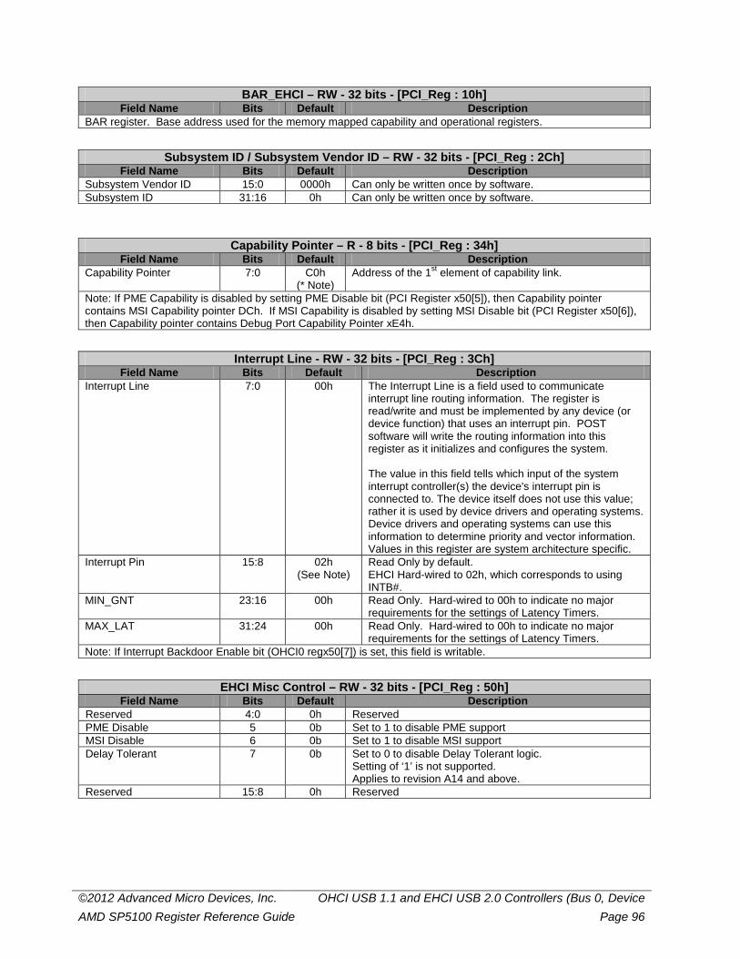
©2012 Advanced Micro Devices, Inc. OHCI USB 1.1 and EHCI USB 2.0 Controllers (Bus 0, Device AMD SP5100 Register Reference Guide Page 96
BAR_EHCI – RW - 32 bits - [PCI_Reg : 10h] Field Name Bits Default Description
BAR register. Base address used for the memory mapped capability and operational registers.
Subsystem ID / Subsystem Vendor ID – RW - 32 bits - [PCI_Reg : 2Ch] Field Name Bits Default Description
Subsystem Vendor ID 15:0 0000h Can only be written once by software. Subsystem ID 31:16 0h Can only be written once by software.
Capability Pointer – R - 8 bits - [PCI_Reg : 34h] Field Name Bits Default Description
Capability Pointer 7:0 C0h (* Note)
Address of the 1st element of capability link.
Note: If PME Capability is disabled by setting PME Disable bit (PCI Register x50[5]), then Capability pointer contains MSI Capability pointer DCh. If MSI Capability is disabled by setting MSI Disable bit (PCI Register x50[6]), then Capability pointer contains Debug Port Capability Pointer xE4h.
Interrupt Line - RW - 32 bits - [PCI_Reg : 3Ch] Field Name Bits Default Description
Interrupt Line 7:0 00h The Interrupt Line is a field used to communicate interrupt line routing information. The register is read/write and must be implemented by any device (or device function) that uses an interrupt pin. POST software will write the routing information into this register as it initializes and configures the system. The value in this field tells which input of the system interrupt controller(s) the device's interrupt pin is connected to. The device itself does not use this value; rather it is used by device drivers and operating systems. Device drivers and operating systems can use this information to determine priority and vector information. Values in this register are system architecture specific.
Interrupt Pin 15:8 02h (See Note)
Read Only by default. EHCI Hard-wired to 02h, which corresponds to using INTB#.
MIN_GNT 23:16 00h Read Only. Hard-wired to 00h to indicate no major requirements for the settings of Latency Timers.
MAX_LAT 31:24 00h Read Only. Hard-wired to 00h to indicate no major requirements for the settings of Latency Timers.
Note: If Interrupt Backdoor Enable bit (OHCI0 regx50[7]) is set, this field is writable.
EHCI Misc Control – RW - 32 bits - [PCI_Reg : 50h] Field Name Bits Default Description
Reserved 4:0 0h Reserved PME Disable 5 0b Set to 1 to disable PME support MSI Disable 6 0b Set to 1 to disable MSI support Delay Tolerant 7 0b Set to 0 to disable Delay Tolerant logic.
Setting of ‘1’ is not supported. Applies to revision A14 and above.
Reserved 15:8 0h Reserved
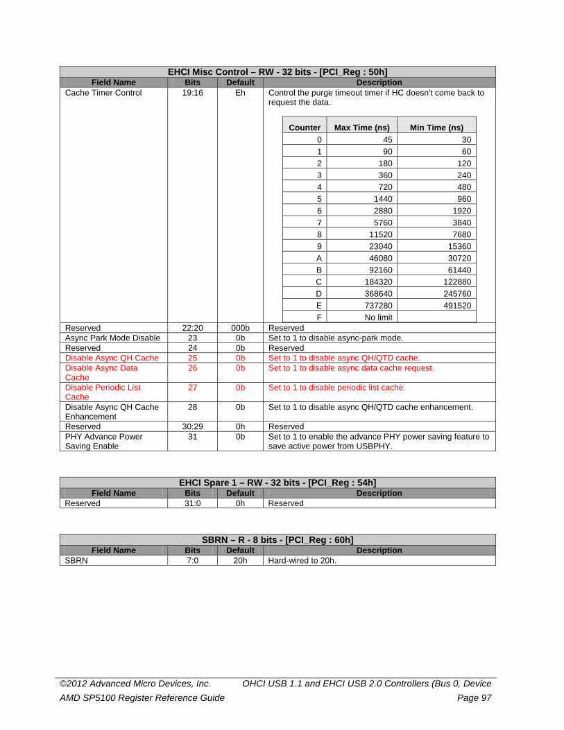
©2012 Advanced Micro Devices, Inc. OHCI USB 1.1 and EHCI USB 2.0 Controllers (Bus 0, Device AMD SP5100 Register Reference Guide Page 97
EHCI Misc Control – RW - 32 bits - [PCI_Reg : 50h] Field Name Bits Default Description
Cache Timer Control 19:16 Eh Control the purge timeout timer if HC doesn't come back to request the data.
Counter Max Time (ns) Min Time (ns) 0 45 30 1 90 60 2 180 120 3 360 240 4 720 480 5 1440 960 6 2880 1920 7 5760 3840 8 11520 7680 9 23040 15360 A 46080 30720 B 92160 61440 C 184320 122880 D 368640 245760 E 737280 491520 F No limit
Reserved 22:20 000b Reserved Async Park Mode Disable 23 0b Set to 1 to disable async-park mode. Reserved 24 0b Reserved Disable Async QH Cache 25 0b Set to 1 to disable async QH/QTD cache. Disable Async Data Cache
26 0b Set to 1 to disable async data cache request.
Disable Periodic List Cache
27 0b Set to 1 to disable periodic list cache.
Disable Async QH Cache Enhancement
28 0b Set to 1 to disable async QH/QTD cache enhancement.
Reserved 30:29 0h Reserved PHY Advance Power Saving Enable
31 0b Set to 1 to enable the advance PHY power saving feature to save active power from USBPHY.
EHCI Spare 1 – RW - 32 bits - [PCI_Reg : 54h] Field Name Bits Default Description
Reserved 31:0 0h Reserved
SBRN – R - 8 bits - [PCI_Reg : 60h] Field Name Bits Default Description
SBRN 7:0 20h Hard-wired to 20h.
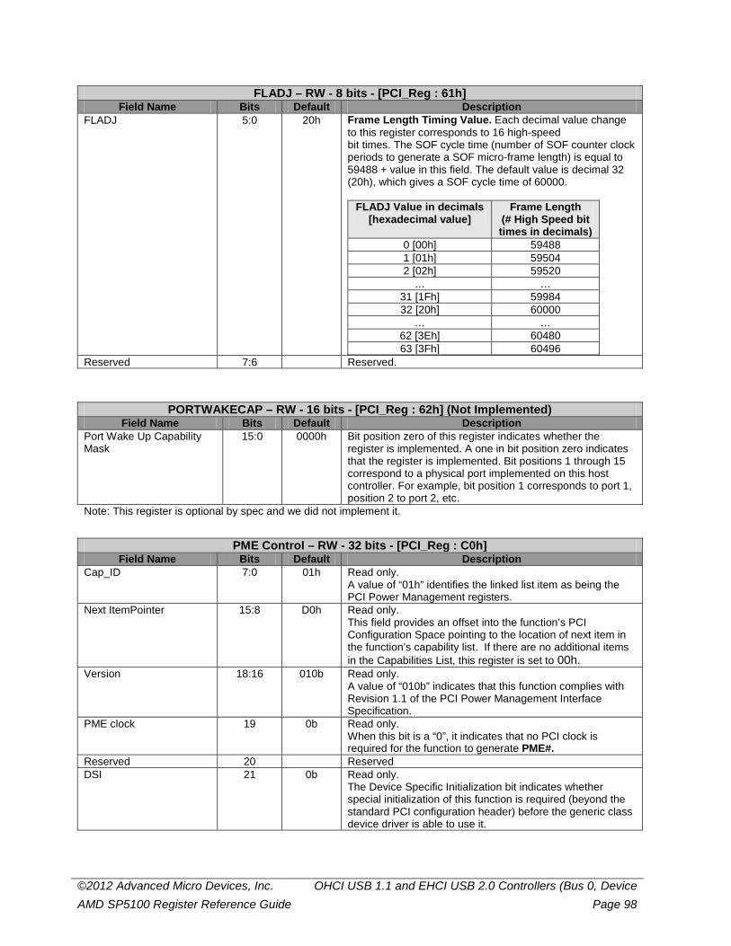
©2012 Advanced Micro Devices, Inc. OHCI USB 1.1 and EHCI USB 2.0 Controllers (Bus 0, Device AMD SP5100 Register Reference Guide Page 98
FLADJ – RW - 8 bits - [PCI_Reg : 61h] Field Name Bits Default Description
FLADJ 5:0 20h Frame Length Timing Value. Each decimal value change to this register corresponds to 16 high-speed bit times. The SOF cycle time (number of SOF counter clock periods to generate a SOF micro-frame length) is equal to 59488 + value in this field. The default value is decimal 32 (20h), which gives a SOF cycle time of 60000.
FLADJ Value in decimals [hexadecimal value]
Frame Length (# High Speed bit times in decimals)
0 [00h] 59488 1 [01h] 59504 2 [02h] 59520
… … 31 [1Fh] 59984 32 [20h] 60000
… … 62 [3Eh] 60480 63 [3Fh] 60496
Reserved 7:6 Reserved.
PORTWAKECAP – RW - 16 bits - [PCI_Reg : 62h] (Not Implemented) Field Name Bits Default Description
Port Wake Up Capability Mask
15:0 0000h Bit position zero of this register indicates whether the register is implemented. A one in bit position zero indicates that the register is implemented. Bit positions 1 through 15 correspond to a physical port implemented on this host controller. For example, bit position 1 corresponds to port 1, position 2 to port 2, etc.
Note: This register is optional by spec and we did not implement it.
PME Control – RW - 32 bits - [PCI_Reg : C0h] Field Name Bits Default Description
Cap_ID 7:0 01h Read only. A value of “01h” identifies the linked list item as being the PCI Power Management registers.
Next ItemPointer 15:8 D0h Read only. This field provides an offset into the function’s PCI Configuration Space pointing to the location of next item in the function’s capability list. If there are no additional items in the Capabilities List, this register is set to 00h.
Version 18:16 010b Read only. A value of “010b” indicates that this function complies with Revision 1.1 of the PCI Power Management Interface Specification.
PME clock 19 0b Read only. When this bit is a “0”, it indicates that no PCI clock is required for the function to generate PME#.
Reserved 20 Reserved DSI 21 0b Read only.
The Device Specific Initialization bit indicates whether special initialization of this function is required (beyond the standard PCI configuration header) before the generic class device driver is able to use it.
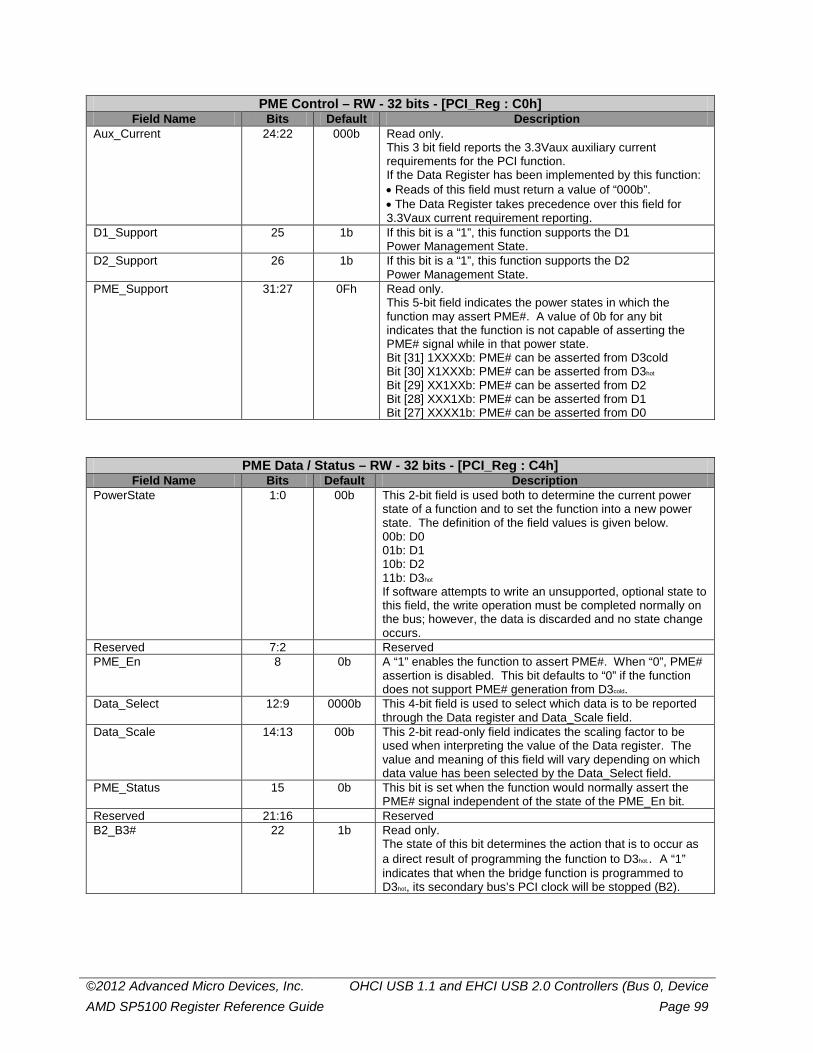
©2012 Advanced Micro Devices, Inc. OHCI USB 1.1 and EHCI USB 2.0 Controllers (Bus 0, Device AMD SP5100 Register Reference Guide Page 99
PME Control – RW - 32 bits - [PCI_Reg : C0h] Field Name Bits Default Description
Aux_Current 24:22 000b Read only. This 3 bit field reports the 3.3Vaux auxiliary current requirements for the PCI function. If the Data Register has been implemented by this function: • Reads of this field must return a value of “000b”. • The Data Register takes precedence over this field for 3.3Vaux current requirement reporting.
D1_Support 25 1b If this bit is a “1”, this function supports the D1 Power Management State.
D2_Support 26 1b If this bit is a “1”, this function supports the D2 Power Management State.
PME_Support 31:27 0Fh Read only. This 5-bit field indicates the power states in which the function may assert PME#. A value of 0b for any bit indicates that the function is not capable of asserting the PME# signal while in that power state. Bit [31] 1XXXXb: PME# can be asserted from D3cold Bit [30] X1XXXb: PME# can be asserted from D3hot
Bit [29] XX1XXb: PME# can be asserted from D2 Bit [28] XXX1Xb: PME# can be asserted from D1 Bit [27] XXXX1b: PME# can be asserted from D0
PME Data / Status – RW - 32 bits - [PCI_Reg : C4h] Field Name Bits Default Description
PowerState 1:0 00b This 2-bit field is used both to determine the current power state of a function and to set the function into a new power state. The definition of the field values is given below. 00b: D0 01b: D1 10b: D2 11b: D3hot
If software attempts to write an unsupported, optional state to this field, the write operation must be completed normally on the bus; however, the data is discarded and no state change occurs.
Reserved 7:2 Reserved PME_En 8 0b A “1” enables the function to assert PME#. When “0”, PME#
assertion is disabled. This bit defaults to “0” if the function does not support PME# generation from D3cold.
Data_Select 12:9 0000b This 4-bit field is used to select which data is to be reported through the Data register and Data_Scale field.
Data_Scale 14:13 00b This 2-bit read-only field indicates the scaling factor to be used when interpreting the value of the Data register. The value and meaning of this field will vary depending on which data value has been selected by the Data_Select field.
PME_Status 15 0b This bit is set when the function would normally assert the PME# signal independent of the state of the PME_En bit.
Reserved 21:16 Reserved B2_B3# 22 1b Read only.
The state of this bit determines the action that is to occur as a direct result of programming the function to D3hot.. A “1” indicates that when the bridge function is programmed to D3hot, its secondary bus’s PCI clock will be stopped (B2).
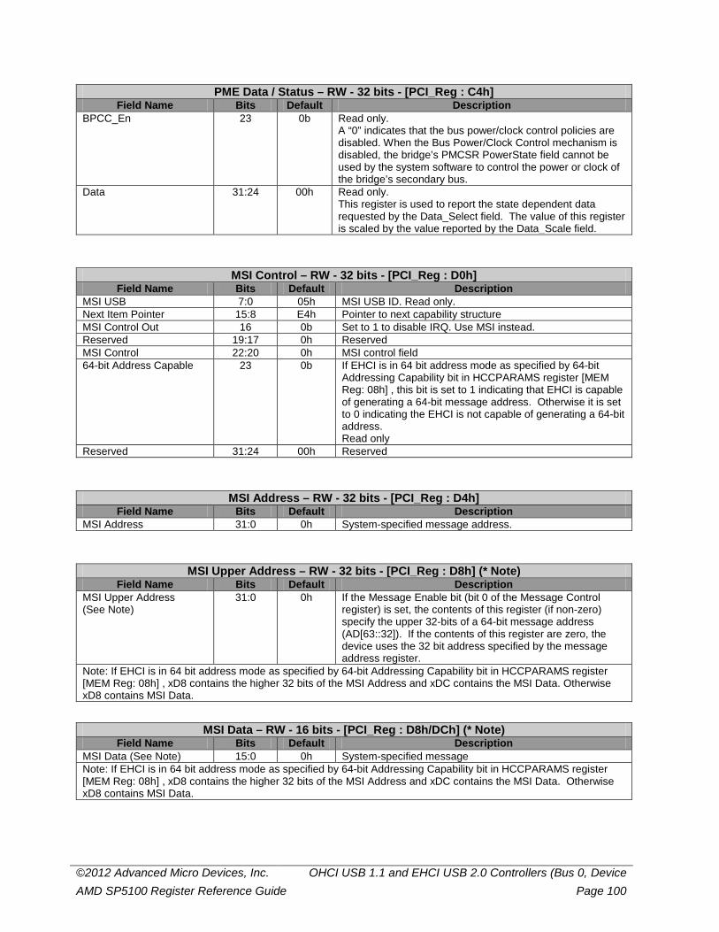
©2012 Advanced Micro Devices, Inc. OHCI USB 1.1 and EHCI USB 2.0 Controllers (Bus 0, Device AMD SP5100 Register Reference Guide Page 100
PME Data / Status – RW - 32 bits - [PCI_Reg : C4h] Field Name Bits Default Description
BPCC_En 23 0b Read only. A “0” indicates that the bus power/clock control policies are disabled. When the Bus Power/Clock Control mechanism is disabled, the bridge’s PMCSR PowerState field cannot be used by the system software to control the power or clock of the bridge’s secondary bus.
Data 31:24 00h Read only. This register is used to report the state dependent data requested by the Data_Select field. The value of this register is scaled by the value reported by the Data_Scale field.
MSI Control – RW - 32 bits - [PCI_Reg : D0h] Field Name Bits Default Description
MSI USB 7:0 05h MSI USB ID. Read only. Next Item Pointer 15:8 E4h Pointer to next capability structure MSI Control Out 16 0b Set to 1 to disable IRQ. Use MSI instead. Reserved 19:17 0h Reserved MSI Control 22:20 0h MSI control field 64-bit Address Capable 23 0b If EHCI is in 64 bit address mode as specified by 64-bit
Addressing Capability bit in HCCPARAMS register [MEM Reg: 08h] , this bit is set to 1 indicating that EHCI is capable of generating a 64-bit message address. Otherwise it is set to 0 indicating the EHCI is not capable of generating a 64-bit address. Read only
Reserved 31:24 00h Reserved
MSI Address – RW - 32 bits - [PCI_Reg : D4h] Field Name Bits Default Description
MSI Address 31:0 0h System-specified message address.
MSI Upper Address – RW - 32 bits - [PCI_Reg : D8h] (* Note) Field Name Bits Default Description
MSI Upper Address (See Note)
31:0 0h If the Message Enable bit (bit 0 of the Message Control register) is set, the contents of this register (if non-zero) specify the upper 32-bits of a 64-bit message address (AD[63::32]). If the contents of this register are zero, the device uses the 32 bit address specified by the message address register.
Note: If EHCI is in 64 bit address mode as specified by 64-bit Addressing Capability bit in HCCPARAMS register [MEM Reg: 08h] , xD8 contains the higher 32 bits of the MSI Address and xDC contains the MSI Data. Otherwise xD8 contains MSI Data.
MSI Data – RW - 16 bits - [PCI_Reg : D8h/DCh] (* Note) Field Name Bits Default Description
MSI Data (See Note) 15:0 0h System-specified message Note: If EHCI is in 64 bit address mode as specified by 64-bit Addressing Capability bit in HCCPARAMS register [MEM Reg: 08h] , xD8 contains the higher 32 bits of the MSI Address and xDC contains the MSI Data. Otherwise xD8 contains MSI Data.
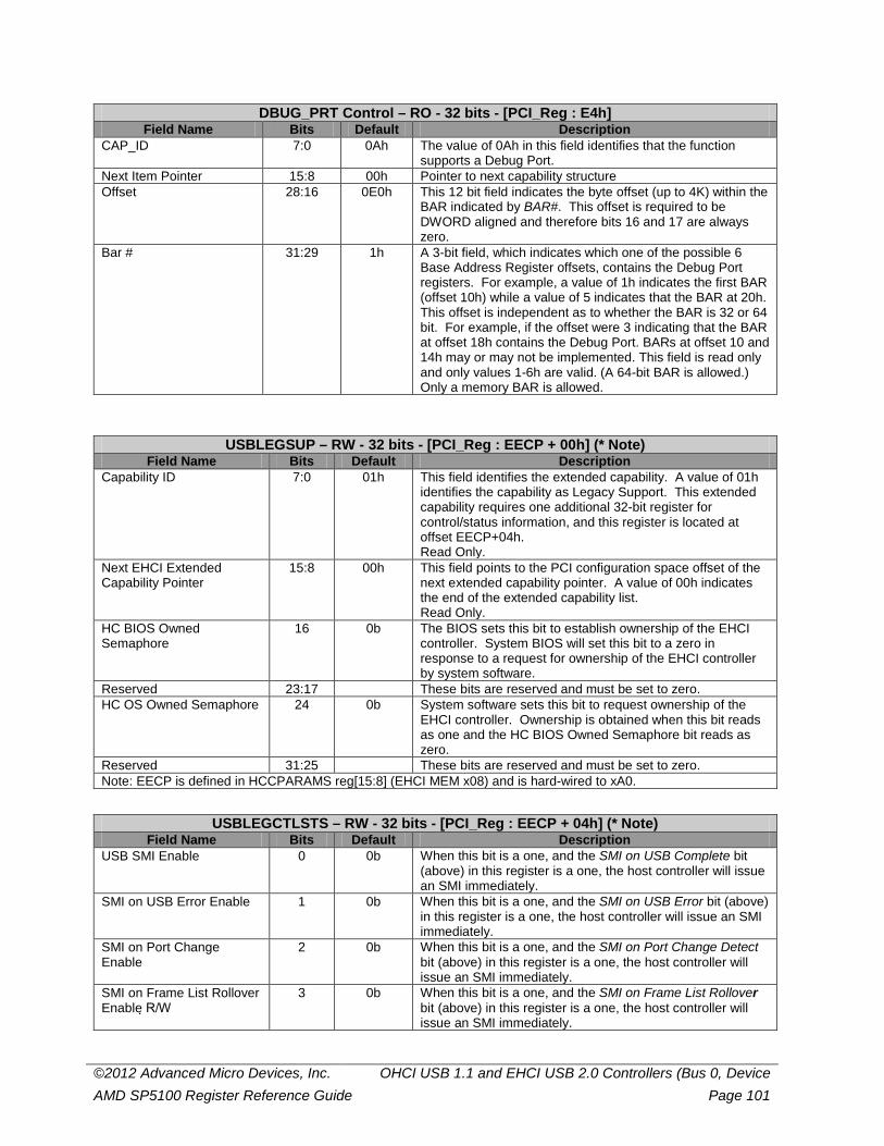
©2012 Advanced Micro Devices, Inc. OHCI USB 1.1 and EHCI USB 2.0 Controllers (Bus 0, Device AMD SP5100 Register Reference Guide Page 101
DBUG_PRT Control – RO - 32 bits - [PCI_Reg : E4h] Field Name Bits Default Description
CAP_ID 7:0 0Ah The value of 0Ah in this field identifies that the function supports a Debug Port.
Next Item Pointer 15:8 00h Pointer to next capability structure Offset 28:16 0E0h This 12 bit field indicates the byte offset (up to 4K) within the
BAR indicated by BAR#. This offset is required to be DWORD aligned and therefore bits 16 and 17 are always zero.
Bar # 31:29 1h A 3-bit field, which indicates which one of the possible 6 Base Address Register offsets, contains the Debug Port registers. For example, a value of 1h indicates the first BAR (offset 10h) while a value of 5 indicates that the BAR at 20h. This offset is independent as to whether the BAR is 32 or 64 bit. For example, if the offset were 3 indicating that the BAR at offset 18h contains the Debug Port. BARs at offset 10 and 14h may or may not be implemented. This field is read only and only values 1-6h are valid. (A 64-bit BAR is allowed.) Only a memory BAR is allowed.
USBLEGSUP – RW - 32 bits - [PCI_Reg : EECP + 00h] (* Note) Field Name Bits Default Description
Capability ID 7:0 01h This field identifies the extended capability. A value of 01h identifies the capability as Legacy Support. This extended capability requires one additional 32-bit register for control/status information, and this register is located at offset EECP+04h. Read Only.
Next EHCI Extended Capability Pointer
15:8 00h This field points to the PCI configuration space offset of the next extended capability pointer. A value of 00h indicates the end of the extended capability list. Read Only.
HC BIOS Owned Semaphore
16 0b The BIOS sets this bit to establish ownership of the EHCI controller. System BIOS will set this bit to a zero in response to a request for ownership of the EHCI controller by system software.
Reserved 23:17 These bits are reserved and must be set to zero. HC OS Owned Semaphore 24 0b System software sets this bit to request ownership of the
EHCI controller. Ownership is obtained when this bit reads as one and the HC BIOS Owned Semaphore bit reads as zero.
Reserved 31:25 These bits are reserved and must be set to zero. Note: EECP is defined in HCCPARAMS reg[15:8] (EHCI MEM x08) and is hard-wired to xA0.
USBLEGCTLSTS – RW - 32 bits - [PCI_Reg : EECP + 04h] (* Note) Field Name Bits Default Description
USB SMI Enable 0 0b When this bit is a one, and the SMI on USB Complete bit (above) in this register is a one, the host controller will issue an SMI immediately.
SMI on USB Error Enable 1 0b When this bit is a one, and the SMI on USB Error bit (above) in this register is a one, the host controller will issue an SMI immediately.
SMI on Port Change Enable
2 0b When this bit is a one, and the SMI on Port Change Detect bit (above) in this register is a one, the host controller will issue an SMI immediately.
SMI on Frame List Rollover Enable R/W
3 0b When this bit is a one, and the SMI on Frame List Rollover bit (above) in this register is a one, the host controller will issue an SMI immediately.
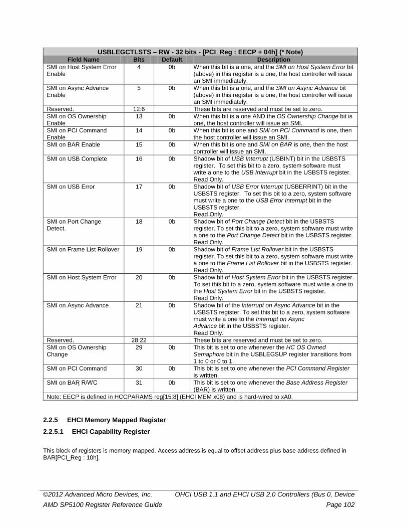
©2012 Advanced Micro Devices, Inc. OHCI USB 1.1 and EHCI USB 2.0 Controllers (Bus 0, Device AMD SP5100 Register Reference Guide Page 102
USBLEGCTLSTS – RW - 32 bits - [PCI_Reg : EECP + 04h] (* Note) Field Name Bits Default Description
SMI on Host System Error Enable
4 0b When this bit is a one, and the SMI on Host System Error bit (above) in this register is a one, the host controller will issue an SMI immediately.
SMI on Async Advance Enable
5 0b When this bit is a one, and the SMI on Async Advance bit (above) in this register is a one, the host controller will issue an SMI immediately.
Reserved. 12:6 These bits are reserved and must be set to zero. SMI on OS Ownership Enable
13 0b When this bit is a one AND the OS Ownership Change bit is one, the host controller will issue an SMI.
SMI on PCI Command Enable
14 0b When this bit is one and SMI on PCI Command is one, then the host controller will issue an SMI.
SMI on BAR Enable 15 0b When this bit is one and SMI on BAR is one, then the host controller will issue an SMI.
SMI on USB Complete 16 0b Shadow bit of USB Interrupt (USBINT) bit in the USBSTS register. To set this bit to a zero, system software must write a one to the USB Interrupt bit in the USBSTS register. Read Only.
SMI on USB Error 17 0b Shadow bit of USB Error Interrupt (USBERRINT) bit in the USBSTS register. To set this bit to a zero, system software must write a one to the USB Error Interrupt bit in the USBSTS register. Read Only.
SMI on Port Change Detect.
18 0b Shadow bit of Port Change Detect bit in the USBSTS register. To set this bit to a zero, system software must write a one to the Port Change Detect bit in the USBSTS register. Read Only.
SMI on Frame List Rollover 19 0b Shadow bit of Frame List Rollover bit in the USBSTS register. To set this bit to a zero, system software must write a one to the Frame List Rollover bit in the USBSTS register. Read Only.
SMI on Host System Error 20 0b Shadow bit of Host System Error bit in the USBSTS register. To set this bit to a zero, system software must write a one to the Host System Error bit in the USBSTS register. Read Only.
SMI on Async Advance 21 0b Shadow bit of the Interrupt on Async Advance bit in the USBSTS register. To set this bit to a zero, system software must write a one to the Interrupt on Async Advance bit in the USBSTS register. Read Only.
Reserved. 28:22 These bits are reserved and must be set to zero. SMI on OS Ownership Change
29 0b This bit is set to one whenever the HC OS Owned Semaphore bit in the USBLEGSUP register transitions from 1 to 0 or 0 to 1.
SMI on PCI Command 30 0b This bit is set to one whenever the PCI Command Register is written.
SMI on BAR R/WC 31 0b This bit is set to one whenever the Base Address Register (BAR) is written.
Note: EECP is defined in HCCPARAMS reg[15:8] (EHCI MEM x08) and is hard-wired to xA0.
2.2.5 EHCI Memory Mapped Register
2.2.5.1 EHCI Capability Register
This block of registers is memory-mapped. Access address is equal to offset address plus base address defined in BAR[PCI_Reg : 10h].
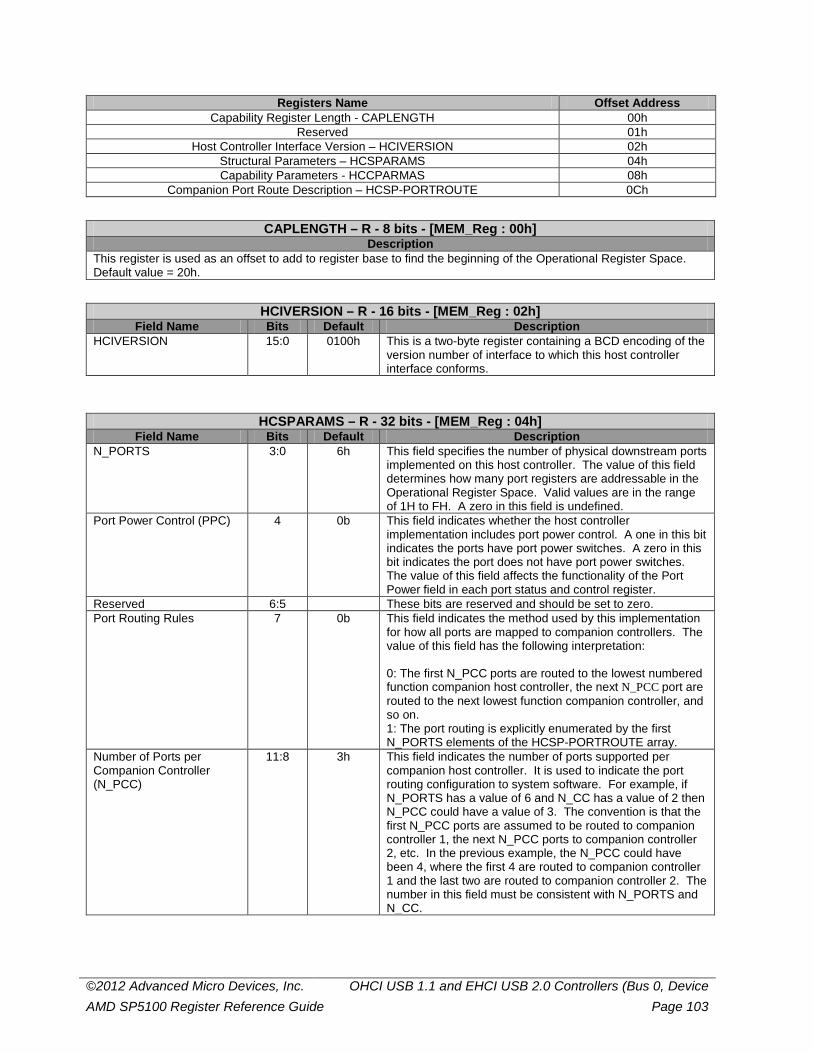
©2012 Advanced Micro Devices, Inc. OHCI USB 1.1 and EHCI USB 2.0 Controllers (Bus 0, Device AMD SP5100 Register Reference Guide Page 103
Registers Name Offset Address Capability Register Length - CAPLENGTH 00h
Reserved 01h Host Controller Interface Version – HCIVERSION 02h
Structural Parameters – HCSPARAMS 04h Capability Parameters - HCCPARMAS 08h
Companion Port Route Description – HCSP-PORTROUTE 0Ch
CAPLENGTH – R - 8 bits - [MEM_Reg : 00h] Description
This register is used as an offset to add to register base to find the beginning of the Operational Register Space. Default value = 20h.
HCIVERSION – R - 16 bits - [MEM_Reg : 02h] Field Name Bits Default Description
HCIVERSION 15:0 0100h This is a two-byte register containing a BCD encoding of the version number of interface to which this host controller interface conforms.
HCSPARAMS – R - 32 bits - [MEM_Reg : 04h] Field Name Bits Default Description
N_PORTS 3:0 6h This field specifies the number of physical downstream ports implemented on this host controller. The value of this field determines how many port registers are addressable in the Operational Register Space. Valid values are in the range of 1H to FH. A zero in this field is undefined.
Port Power Control (PPC) 4 0b This field indicates whether the host controller implementation includes port power control. A one in this bit indicates the ports have port power switches. A zero in this bit indicates the port does not have port power switches. The value of this field affects the functionality of the Port Power field in each port status and control register.
Reserved 6:5 These bits are reserved and should be set to zero. Port Routing Rules 7 0b This field indicates the method used by this implementation
for how all ports are mapped to companion controllers. The value of this field has the following interpretation: 0: The first N_PCC ports are routed to the lowest numbered function companion host controller, the next N_PCC port are routed to the next lowest function companion controller, and so on. 1: The port routing is explicitly enumerated by the first N_PORTS elements of the HCSP-PORTROUTE array.
Number of Ports per Companion Controller (N_PCC)
11:8 3h This field indicates the number of ports supported per companion host controller. It is used to indicate the port routing configuration to system software. For example, if N_PORTS has a value of 6 and N_CC has a value of 2 then N_PCC could have a value of 3. The convention is that the first N_PCC ports are assumed to be routed to companion controller 1, the next N_PCC ports to companion controller 2, etc. In the previous example, the N_PCC could have been 4, where the first 4 are routed to companion controller 1 and the last two are routed to companion controller 2. The number in this field must be consistent with N_PORTS and N_CC.
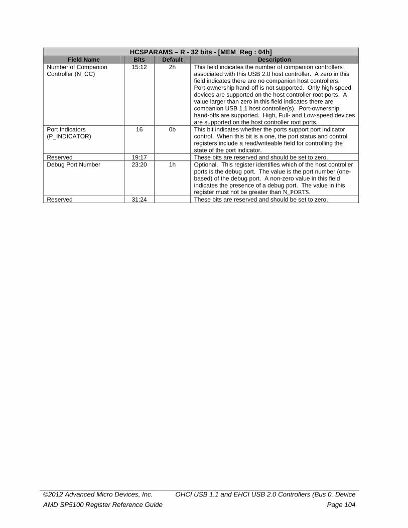
©2012 Advanced Micro Devices, Inc. OHCI USB 1.1 and EHCI USB 2.0 Controllers (Bus 0, Device AMD SP5100 Register Reference Guide Page 104
HCSPARAMS – R - 32 bits - [MEM_Reg : 04h] Field Name Bits Default Description
Number of Companion Controller (N_CC)
15:12 2h This field indicates the number of companion controllers associated with this USB 2.0 host controller. A zero in this field indicates there are no companion host controllers. Port-ownership hand-off is not supported. Only high-speed devices are supported on the host controller root ports. A value larger than zero in this field indicates there are companion USB 1.1 host controller(s). Port-ownership hand-offs are supported. High, Full- and Low-speed devices are supported on the host controller root ports.
Port Indicators (P_INDICATOR)
16 0b This bit indicates whether the ports support port indicator control. When this bit is a one, the port status and control registers include a read/writeable field for controlling the state of the port indicator.
Reserved 19:17 These bits are reserved and should be set to zero. Debug Port Number 23:20 1h
Optional. This register identifies which of the host controller ports is the debug port. The value is the port number (one-based) of the debug port. A non-zero value in this field indicates the presence of a debug port. The value in this register must not be greater than N_PORTS.
Reserved 31:24 These bits are reserved and should be set to zero.
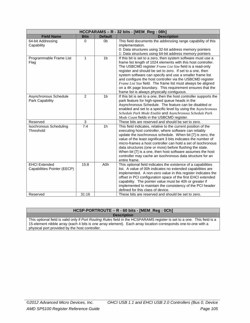
©2012 Advanced Micro Devices, Inc. OHCI USB 1.1 and EHCI USB 2.0 Controllers (Bus 0, Device AMD SP5100 Register Reference Guide Page 105
HCCPARAMS – R - 32 bits - [MEM_Reg : 08h] Field Name Bits Default Description
64-bit Addressing Capability
0 0b This field documents the addressing range capability of this implementation. 0: Data structures using 32-bit address memory pointers 1: Data structures using 64-bit address memory pointers
Programmable Frame List Flag
1 1b If this bit is set to a zero, then system software must use a frame list length of 1024 elements with this host controller. The USBCMD register Frame List Size field is a read-only register and should be set to zero. If set to a one, then system software can specify and use a smaller frame list and configure the host controller via the USBCMD register Frame List Size field. The frame list must always be aligned on a 4K page boundary. This requirement ensures that the frame list is always physically contiguous.
Asynchronous Schedule Park Capability
2 1b If this bit is set to a one, then the host controller supports the park feature for high-speed queue heads in the Asynchronous Schedule. The feature can be disabled or enabled and set to a specific level by using the Asynchronous Schedule Park Mode Enable and Asynchronous Schedule Park Mode Count fields in the USBCMD register.
Reserved 3 These bits are reserved and should be set to zero. Isochronous Scheduling Threshold
7:4 1h This field indicates, relative to the current position of the executing host controller, where software can reliably update the isochronous schedule. When bit [7] is zero, the value of the least significant 3 bits indicates the number of micro-frames a host controller can hold a set of isochronous data structures (one or more) before flushing the state. When bit [7] is a one, then host software assumes the host controller may cache an isochronous data structure for an entire frame.
EHCI Extended Capabilities Pointer (EECP)
15:8 A0h This optional field indicates the existence of a capabilities list. A value of 00h indicates no extended capabilities are implemented. A non-zero value in this register indicates the offset in PCI configuration space of the first EHCI extended capability. The pointer value must be 40h or greater if implemented to maintain the consistency of the PCI header defined for this class of device.
Reserved 31:16 These bits are reserved and should be set to zero.
HCSP-PORTROUTE – R - 60 bits - [MEM_Reg : 0Ch] Description
This optional field is valid only if Port Routing Rules field in the HCSPARAMS register is set to a one. This field is a 15-element nibble array (each 4 bits is one array element). Each array location corresponds one-to-one with a physical port provided by the host controller.
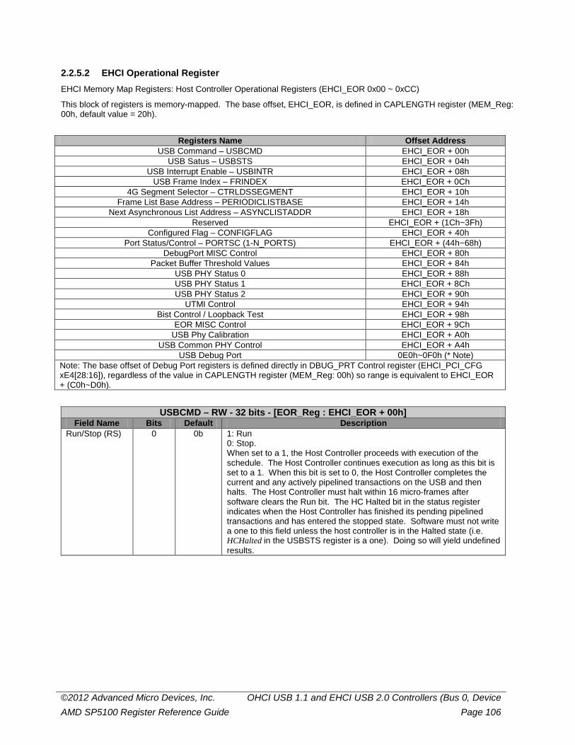
©2012 Advanced Micro Devices, Inc. OHCI USB 1.1 and EHCI USB 2.0 Controllers (Bus 0, Device AMD SP5100 Register Reference Guide Page 106
2.2.5.2 EHCI Operational Register EHCI Memory Map Registers: Host Controller Operational Registers (EHCI_EOR 0x00 ~ 0xCC)
This block of registers is memory-mapped. The base offset, EHCI_EOR, is defined in CAPLENGTH register (MEM_Reg: 00h, default value = 20h).
Registers Name Offset Address USB Command – USBCMD EHCI_EOR + 00h
USB Satus – USBSTS EHCI_EOR + 04h USB Interrupt Enable – USBINTR EHCI_EOR + 08h
USB Frame Index – FRINDEX EHCI_EOR + 0Ch 4G Segment Selector – CTRLDSSEGMENT EHCI_EOR + 10h
Frame List Base Address – PERIODICLISTBASE EHCI_EOR + 14h Next Asynchronous List Address – ASYNCLISTADDR EHCI_EOR + 18h
Reserved EHCI_EOR + (1Ch~3Fh) Configured Flag – CONFIGFLAG EHCI_EOR + 40h
Port Status/Control – PORTSC (1-N_PORTS) EHCI_EOR + (44h~68h) DebugPort MISC Control EHCI_EOR + 80h
Packet Buffer Threshold Values EHCI_EOR + 84h USB PHY Status 0 EHCI_EOR + 88h USB PHY Status 1 EHCI_EOR + 8Ch USB PHY Status 2 EHCI_EOR + 90h
UTMI Control EHCI_EOR + 94h Bist Control / Loopback Test EHCI_EOR + 98h
EOR MISC Control EHCI_EOR + 9Ch USB Phy Calibration EHCI_EOR + A0h
USB Common PHY Control EHCI_EOR + A4h USB Debug Port 0E0h~0F0h (* Note)
Note: The base offset of Debug Port registers is defined directly in DBUG_PRT Control register (EHCI_PCI_CFG xE4[28:16]), regardless of the value in CAPLENGTH register (MEM_Reg: 00h) so range is equivalent to EHCI_EOR + (C0h~D0h).
USBCMD – RW - 32 bits - [EOR_Reg : EHCI_EOR + 00h] Field Name Bits Default Description
Run/Stop (RS)
0 0b 1: Run 0: Stop. When set to a 1, the Host Controller proceeds with execution of the schedule. The Host Controller continues execution as long as this bit is set to a 1. When this bit is set to 0, the Host Controller completes the current and any actively pipelined transactions on the USB and then halts. The Host Controller must halt within 16 micro-frames after software clears the Run bit. The HC Halted bit in the status register indicates when the Host Controller has finished its pending pipelined transactions and has entered the stopped state. Software must not write a one to this field unless the host controller is in the Halted state (i.e. HCHalted in the USBSTS register is a one). Doing so will yield undefined results.
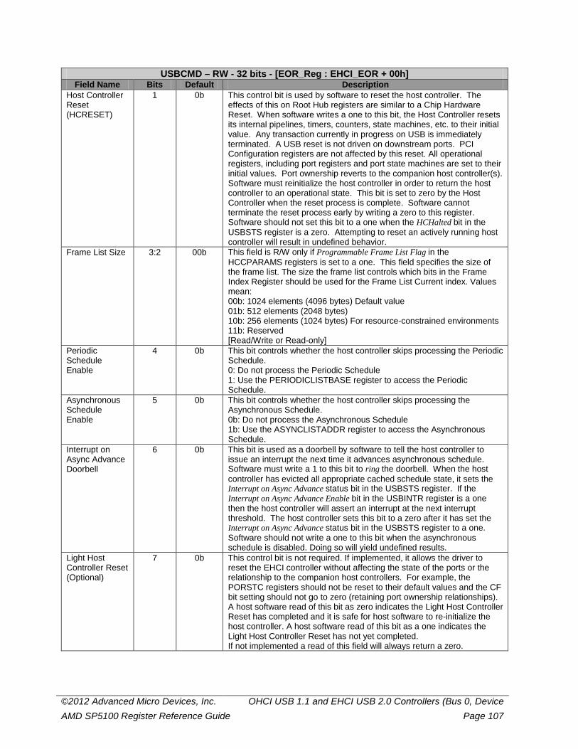
©2012 Advanced Micro Devices, Inc. OHCI USB 1.1 and EHCI USB 2.0 Controllers (Bus 0, Device AMD SP5100 Register Reference Guide Page 107
USBCMD – RW - 32 bits - [EOR_Reg : EHCI_EOR + 00h] Field Name Bits Default Description
Host Controller Reset (HCRESET)
1 0b This control bit is used by software to reset the host controller. The effects of this on Root Hub registers are similar to a Chip Hardware Reset. When software writes a one to this bit, the Host Controller resets its internal pipelines, timers, counters, state machines, etc. to their initial value. Any transaction currently in progress on USB is immediately terminated. A USB reset is not driven on downstream ports. PCI Configuration registers are not affected by this reset. All operational registers, including port registers and port state machines are set to their initial values. Port ownership reverts to the companion host controller(s). Software must reinitialize the host controller in order to return the host controller to an operational state. This bit is set to zero by the Host Controller when the reset process is complete. Software cannot terminate the reset process early by writing a zero to this register. Software should not set this bit to a one when the HCHalted bit in the USBSTS register is a zero. Attempting to reset an actively running host controller will result in undefined behavior.
Frame List Size 3:2 00b This field is R/W only if Programmable Frame List Flag in the HCCPARAMS registers is set to a one. This field specifies the size of the frame list. The size the frame list controls which bits in the Frame Index Register should be used for the Frame List Current index. Values mean: 00b: 1024 elements (4096 bytes) Default value 01b: 512 elements (2048 bytes) 10b: 256 elements (1024 bytes) For resource-constrained environments 11b: Reserved [Read/Write or Read-only]
Periodic Schedule Enable
4 0b This bit controls whether the host controller skips processing the Periodic Schedule. 0: Do not process the Periodic Schedule 1: Use the PERIODICLISTBASE register to access the Periodic Schedule.
Asynchronous Schedule Enable
5 0b This bit controls whether the host controller skips processing the Asynchronous Schedule. 0b: Do not process the Asynchronous Schedule 1b: Use the ASYNCLISTADDR register to access the Asynchronous Schedule.
Interrupt on Async Advance Doorbell
6 0b This bit is used as a doorbell by software to tell the host controller to issue an interrupt the next time it advances asynchronous schedule. Software must write a 1 to this bit to ring the doorbell. When the host controller has evicted all appropriate cached schedule state, it sets the Interrupt on Async Advance status bit in the USBSTS register. If the Interrupt on Async Advance Enable bit in the USBINTR register is a one then the host controller will assert an interrupt at the next interrupt threshold. The host controller sets this bit to a zero after it has set the Interrupt on Async Advance status bit in the USBSTS register to a one. Software should not write a one to this bit when the asynchronous schedule is disabled. Doing so will yield undefined results.
Light Host Controller Reset (Optional)
7 0b This control bit is not required. If implemented, it allows the driver to reset the EHCI controller without affecting the state of the ports or the relationship to the companion host controllers. For example, the PORSTC registers should not be reset to their default values and the CF bit setting should not go to zero (retaining port ownership relationships). A host software read of this bit as zero indicates the Light Host Controller Reset has completed and it is safe for host software to re-initialize the host controller. A host software read of this bit as a one indicates the Light Host Controller Reset has not yet completed. If not implemented a read of this field will always return a zero.
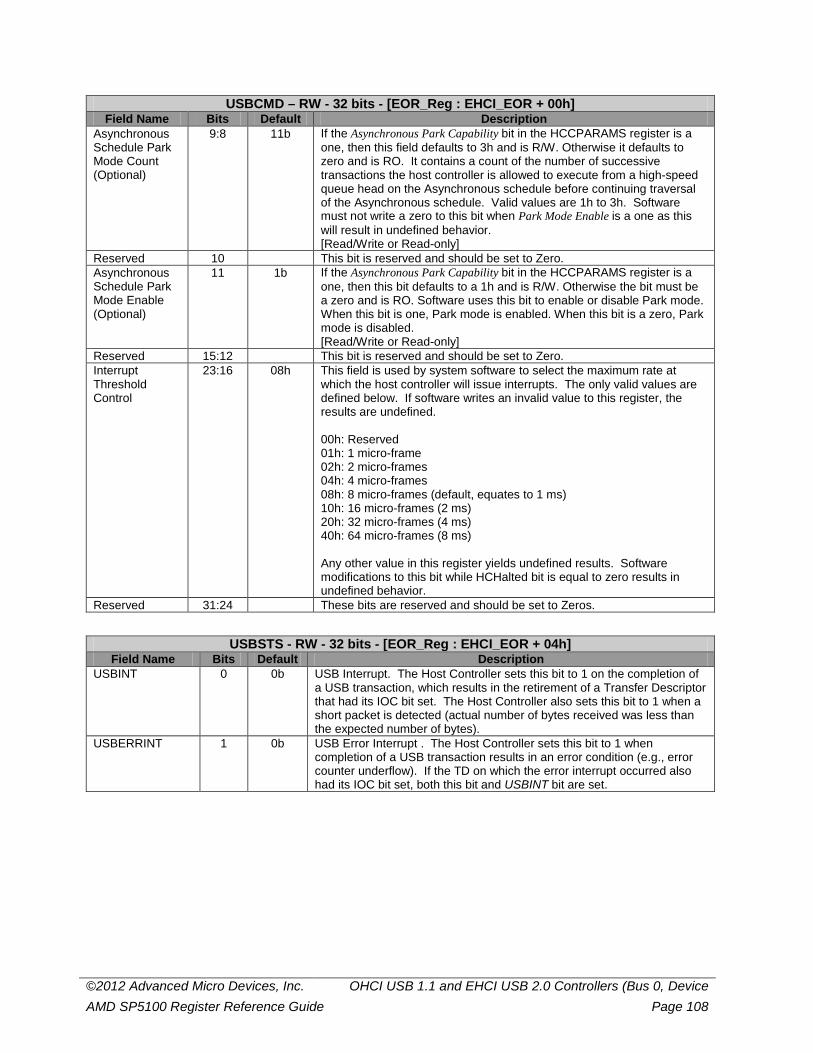
©2012 Advanced Micro Devices, Inc. OHCI USB 1.1 and EHCI USB 2.0 Controllers (Bus 0, Device AMD SP5100 Register Reference Guide Page 108
USBCMD – RW - 32 bits - [EOR_Reg : EHCI_EOR + 00h] Field Name Bits Default Description
Asynchronous Schedule Park Mode Count (Optional)
9:8 11b If the Asynchronous Park Capability bit in the HCCPARAMS register is a one, then this field defaults to 3h and is R/W. Otherwise it defaults to zero and is RO. It contains a count of the number of successive transactions the host controller is allowed to execute from a high-speed queue head on the Asynchronous schedule before continuing traversal of the Asynchronous schedule. Valid values are 1h to 3h. Software must not write a zero to this bit when Park Mode Enable is a one as this will result in undefined behavior. [Read/Write or Read-only]
Reserved 10 This bit is reserved and should be set to Zero. Asynchronous Schedule Park Mode Enable (Optional)
11 1b If the Asynchronous Park Capability bit in the HCCPARAMS register is a one, then this bit defaults to a 1h and is R/W. Otherwise the bit must be a zero and is RO. Software uses this bit to enable or disable Park mode. When this bit is one, Park mode is enabled. When this bit is a zero, Park mode is disabled. [Read/Write or Read-only]
Reserved 15:12 This bit is reserved and should be set to Zero. Interrupt Threshold Control
23:16 08h This field is used by system software to select the maximum rate at which the host controller will issue interrupts. The only valid values are defined below. If software writes an invalid value to this register, the results are undefined. 00h: Reserved 01h: 1 micro-frame 02h: 2 micro-frames 04h: 4 micro-frames 08h: 8 micro-frames (default, equates to 1 ms) 10h: 16 micro-frames (2 ms) 20h: 32 micro-frames (4 ms) 40h: 64 micro-frames (8 ms) Any other value in this register yields undefined results. Software modifications to this bit while HCHalted bit is equal to zero results in undefined behavior.
Reserved 31:24 These bits are reserved and should be set to Zeros.
USBSTS - RW - 32 bits - [EOR_Reg : EHCI_EOR + 04h] Field Name Bits Default Description
USBINT 0 0b USB Interrupt. The Host Controller sets this bit to 1 on the completion of a USB transaction, which results in the retirement of a Transfer Descriptor that had its IOC bit set. The Host Controller also sets this bit to 1 when a short packet is detected (actual number of bytes received was less than the expected number of bytes).
USBERRINT 1 0b USB Error Interrupt . The Host Controller sets this bit to 1 when completion of a USB transaction results in an error condition (e.g., error counter underflow). If the TD on which the error interrupt occurred also had its IOC bit set, both this bit and USBINT bit are set.
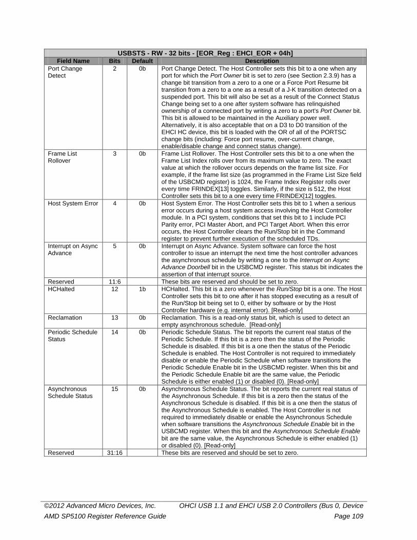
©2012 Advanced Micro Devices, Inc. OHCI USB 1.1 and EHCI USB 2.0 Controllers (Bus 0, Device AMD SP5100 Register Reference Guide Page 109
USBSTS - RW - 32 bits - [EOR_Reg : EHCI_EOR + 04h] Field Name Bits Default Description
Port Change Detect
2 0b Port Change Detect. The Host Controller sets this bit to a one when any port for which the Port Owner bit is set to zero (see Section 2.3.9) has a change bit transition from a zero to a one or a Force Port Resume bit transition from a zero to a one as a result of a J-K transition detected on a suspended port. This bit will also be set as a result of the Connect Status Change being set to a one after system software has relinquished ownership of a connected port by writing a zero to a port's Port Owner bit. This bit is allowed to be maintained in the Auxiliary power well. Alternatively, it is also acceptable that on a D3 to D0 transition of the EHCI HC device, this bit is loaded with the OR of all of the PORTSC change bits (including: Force port resume, over-current change, enable/disable change and connect status change).
Frame List Rollover
3 0b Frame List Rollover. The Host Controller sets this bit to a one when the Frame List Index rolls over from its maximum value to zero. The exact value at which the rollover occurs depends on the frame list size. For example, if the frame list size (as programmed in the Frame List Size field of the USBCMD register) is 1024, the Frame Index Register rolls over every time FRINDEX[13] toggles. Similarly, if the size is 512, the Host Controller sets this bit to a one every time FRINDEX[12] toggles.
Host System Error 4 0b Host System Error. The Host Controller sets this bit to 1 when a serious error occurs during a host system access involving the Host Controller module. In a PCI system, conditions that set this bit to 1 include PCI Parity error, PCI Master Abort, and PCI Target Abort. When this error occurs, the Host Controller clears the Run/Stop bit in the Command register to prevent further execution of the scheduled TDs.
Interrupt on Async Advance
5 0b Interrupt on Async Advance. System software can force the host controller to issue an interrupt the next time the host controller advances the asynchronous schedule by writing a one to the Interrupt on Async Advance Doorbell bit in the USBCMD register. This status bit indicates the assertion of that interrupt source.
Reserved 11:6 These bits are reserved and should be set to zero. HCHalted 12 1b HCHalted. This bit is a zero whenever the Run/Stop bit is a one. The Host
Controller sets this bit to one after it has stopped executing as a result of the Run/Stop bit being set to 0, either by software or by the Host Controller hardware (e.g. internal error). [Read-only]
Reclamation 13 0b Reclamation. This is a read-only status bit, which is used to detect an empty asynchronous schedule. [Read-only]
Periodic Schedule Status
14 0b Periodic Schedule Status. The bit reports the current real status of the Periodic Schedule. If this bit is a zero then the status of the Periodic Schedule is disabled. If this bit is a one then the status of the Periodic Schedule is enabled. The Host Controller is not required to immediately disable or enable the Periodic Schedule when software transitions the Periodic Schedule Enable bit in the USBCMD register. When this bit and the Periodic Schedule Enable bit are the same value, the Periodic Schedule is either enabled (1) or disabled (0). [Read-only]
Asynchronous Schedule Status
15 0b Asynchronous Schedule Status. The bit reports the current real status of the Asynchronous Schedule. If this bit is a zero then the status of the Asynchronous Schedule is disabled. If this bit is a one then the status of the Asynchronous Schedule is enabled. The Host Controller is not required to immediately disable or enable the Asynchronous Schedule when software transitions the Asynchronous Schedule Enable bit in the USBCMD register. When this bit and the Asynchronous Schedule Enable bit are the same value, the Asynchronous Schedule is either enabled (1) or disabled (0). [Read-only]
Reserved 31:16 These bits are reserved and should be set to zero.
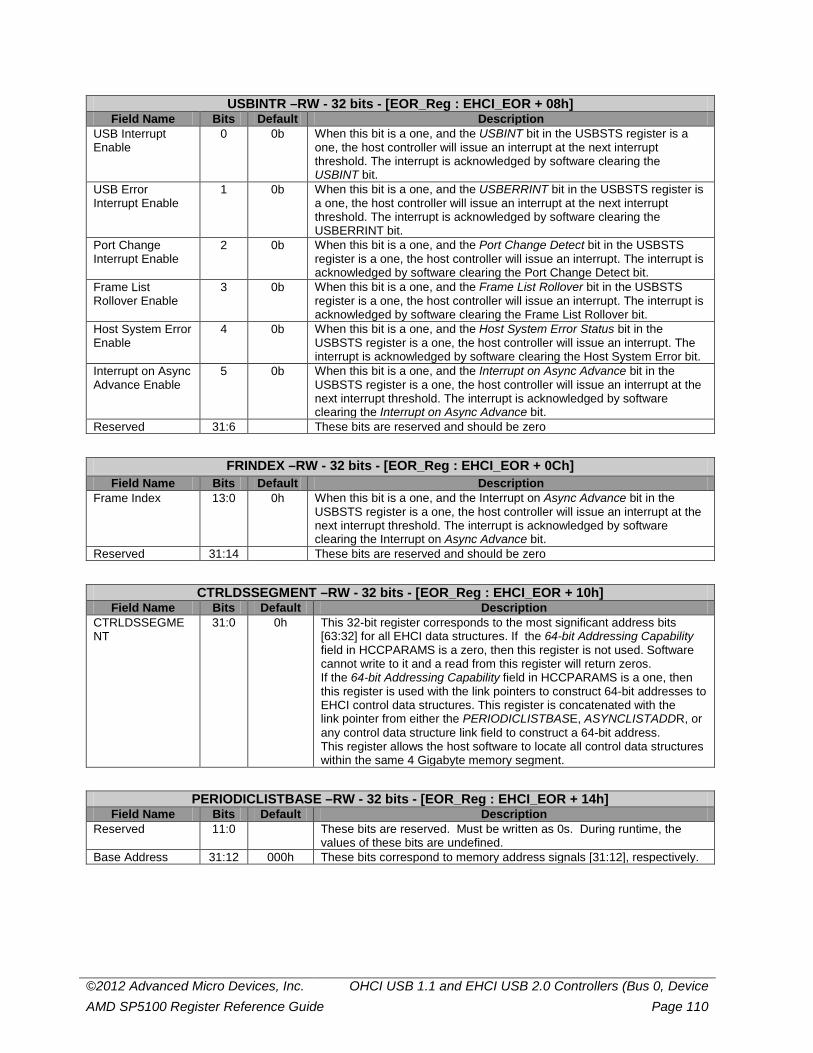
©2012 Advanced Micro Devices, Inc. OHCI USB 1.1 and EHCI USB 2.0 Controllers (Bus 0, Device AMD SP5100 Register Reference Guide Page 110
USBINTR –RW - 32 bits - [EOR_Reg : EHCI_EOR + 08h] Field Name Bits Default Description
USB Interrupt Enable
0 0b When this bit is a one, and the USBINT bit in the USBSTS register is a one, the host controller will issue an interrupt at the next interrupt threshold. The interrupt is acknowledged by software clearing the USBINT bit.
USB Error Interrupt Enable
1 0b When this bit is a one, and the USBERRINT bit in the USBSTS register is a one, the host controller will issue an interrupt at the next interrupt threshold. The interrupt is acknowledged by software clearing the USBERRINT bit.
Port Change Interrupt Enable
2 0b When this bit is a one, and the Port Change Detect bit in the USBSTS register is a one, the host controller will issue an interrupt. The interrupt is acknowledged by software clearing the Port Change Detect bit.
Frame List Rollover Enable
3 0b When this bit is a one, and the Frame List Rollover bit in the USBSTS register is a one, the host controller will issue an interrupt. The interrupt is acknowledged by software clearing the Frame List Rollover bit.
Host System Error Enable
4 0b When this bit is a one, and the Host System Error Status bit in the USBSTS register is a one, the host controller will issue an interrupt. The interrupt is acknowledged by software clearing the Host System Error bit.
Interrupt on Async Advance Enable
5 0b When this bit is a one, and the Interrupt on Async Advance bit in the USBSTS register is a one, the host controller will issue an interrupt at the next interrupt threshold. The interrupt is acknowledged by software clearing the Interrupt on Async Advance bit.
Reserved 31:6 These bits are reserved and should be zero
FRINDEX –RW - 32 bits - [EOR_Reg : EHCI_EOR + 0Ch] Field Name Bits Default Description
Frame Index 13:0 0h When this bit is a one, and the Interrupt on Async Advance bit in the USBSTS register is a one, the host controller will issue an interrupt at the next interrupt threshold. The interrupt is acknowledged by software clearing the Interrupt on Async Advance bit.
Reserved 31:14 These bits are reserved and should be zero
CTRLDSSEGMENT –RW - 32 bits - [EOR_Reg : EHCI_EOR + 10h] Field Name Bits Default Description
CTRLDSSEGMENT
31:0 0h This 32-bit register corresponds to the most significant address bits [63:32] for all EHCI data structures. If the 64-bit Addressing Capability field in HCCPARAMS is a zero, then this register is not used. Software cannot write to it and a read from this register will return zeros. If the 64-bit Addressing Capability field in HCCPARAMS is a one, then this register is used with the link pointers to construct 64-bit addresses to EHCI control data structures. This register is concatenated with the link pointer from either the PERIODICLISTBASE, ASYNCLISTADDR, or any control data structure link field to construct a 64-bit address. This register allows the host software to locate all control data structures within the same 4 Gigabyte memory segment.
PERIODICLISTBASE –RW - 32 bits - [EOR_Reg : EHCI_EOR + 14h] Field Name Bits Default Description
Reserved 11:0 These bits are reserved. Must be written as 0s. During runtime, the values of these bits are undefined.
Base Address 31:12 000h These bits correspond to memory address signals [31:12], respectively.
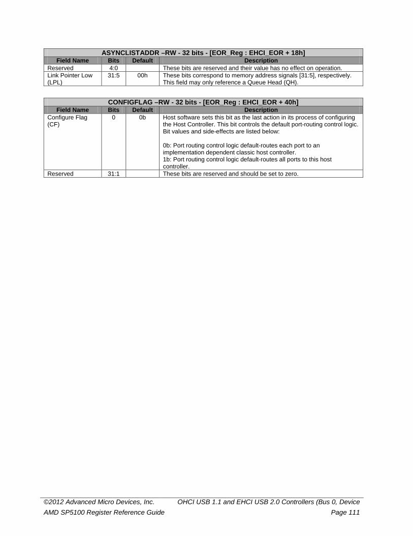
©2012 Advanced Micro Devices, Inc. OHCI USB 1.1 and EHCI USB 2.0 Controllers (Bus 0, Device AMD SP5100 Register Reference Guide Page 111
ASYNCLISTADDR –RW - 32 bits - [EOR_Reg : EHCI_EOR + 18h] Field Name Bits Default Description
Reserved 4:0 These bits are reserved and their value has no effect on operation. Link Pointer Low (LPL)
31:5 00h These bits correspond to memory address signals [31:5], respectively. This field may only reference a Queue Head (QH).
CONFIGFLAG –RW - 32 bits - [EOR_Reg : EHCI_EOR + 40h] Field Name Bits Default Description
Configure Flag (CF)
0 0b Host software sets this bit as the last action in its process of configuring the Host Controller. This bit controls the default port-routing control logic. Bit values and side-effects are listed below: 0b: Port routing control logic default-routes each port to an implementation dependent classic host controller. 1b: Port routing control logic default-routes all ports to this host controller.
Reserved 31:1 These bits are reserved and should be set to zero.
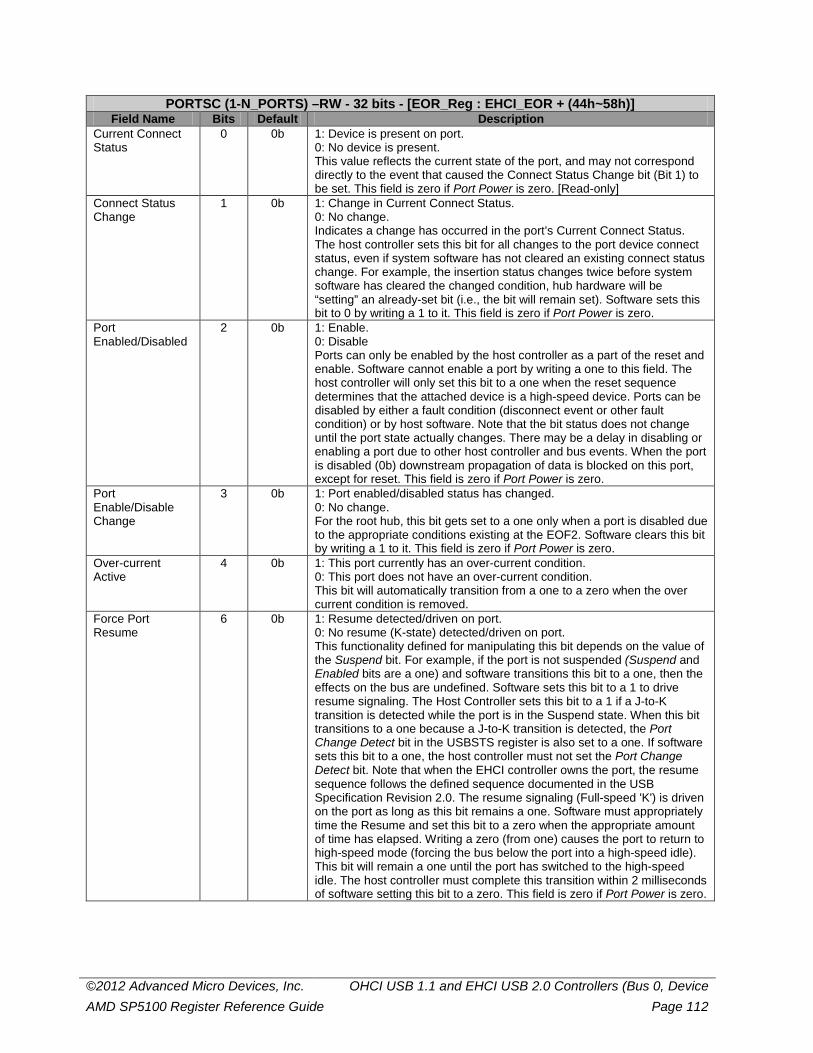
©2012 Advanced Micro Devices, Inc. OHCI USB 1.1 and EHCI USB 2.0 Controllers (Bus 0, Device AMD SP5100 Register Reference Guide Page 112
PORTSC (1-N_PORTS) –RW - 32 bits - [EOR_Reg : EHCI_EOR + (44h~58h)] Field Name Bits Default Description
Current Connect Status
0 0b 1: Device is present on port. 0: No device is present. This value reflects the current state of the port, and may not correspond directly to the event that caused the Connect Status Change bit (Bit 1) to be set. This field is zero if Port Power is zero. [Read-only]
Connect Status Change
1 0b 1: Change in Current Connect Status. 0: No change. Indicates a change has occurred in the port’s Current Connect Status. The host controller sets this bit for all changes to the port device connect status, even if system software has not cleared an existing connect status change. For example, the insertion status changes twice before system software has cleared the changed condition, hub hardware will be “setting” an already-set bit (i.e., the bit will remain set). Software sets this bit to 0 by writing a 1 to it. This field is zero if Port Power is zero.
Port Enabled/Disabled
2 0b 1: Enable. 0: Disable Ports can only be enabled by the host controller as a part of the reset and enable. Software cannot enable a port by writing a one to this field. The host controller will only set this bit to a one when the reset sequence determines that the attached device is a high-speed device. Ports can be disabled by either a fault condition (disconnect event or other fault condition) or by host software. Note that the bit status does not change until the port state actually changes. There may be a delay in disabling or enabling a port due to other host controller and bus events. When the port is disabled (0b) downstream propagation of data is blocked on this port, except for reset. This field is zero if Port Power is zero.
Port Enable/Disable Change
3 0b 1: Port enabled/disabled status has changed. 0: No change. For the root hub, this bit gets set to a one only when a port is disabled due to the appropriate conditions existing at the EOF2. Software clears this bit by writing a 1 to it. This field is zero if Port Power is zero.
Over-current Active
4 0b 1: This port currently has an over-current condition. 0: This port does not have an over-current condition. This bit will automatically transition from a one to a zero when the over current condition is removed.
Force Port Resume
6 0b 1: Resume detected/driven on port. 0: No resume (K-state) detected/driven on port. This functionality defined for manipulating this bit depends on the value of the Suspend bit. For example, if the port is not suspended (Suspend and Enabled bits are a one) and software transitions this bit to a one, then the effects on the bus are undefined. Software sets this bit to a 1 to drive resume signaling. The Host Controller sets this bit to a 1 if a J-to-K transition is detected while the port is in the Suspend state. When this bit transitions to a one because a J-to-K transition is detected, the Port Change Detect bit in the USBSTS register is also set to a one. If software sets this bit to a one, the host controller must not set the Port Change Detect bit. Note that when the EHCI controller owns the port, the resume sequence follows the defined sequence documented in the USB Specification Revision 2.0. The resume signaling (Full-speed 'K') is driven on the port as long as this bit remains a one. Software must appropriately time the Resume and set this bit to a zero when the appropriate amount of time has elapsed. Writing a zero (from one) causes the port to return to high-speed mode (forcing the bus below the port into a high-speed idle). This bit will remain a one until the port has switched to the high-speed idle. The host controller must complete this transition within 2 milliseconds of software setting this bit to a zero. This field is zero if Port Power is zero.
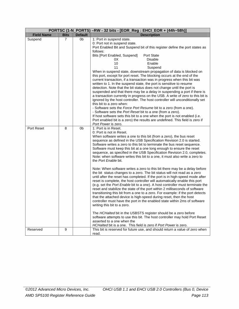
©2012 Advanced Micro Devices, Inc. OHCI USB 1.1 and EHCI USB 2.0 Controllers (Bus 0, Device AMD SP5100 Register Reference Guide Page 113
PORTSC (1-N_PORTS) –RW - 32 bits - [EOR_Reg : EHCI_EOR + (44h~58h)] Field Name Bits Default Description
Suspend 7 0b 1: Port in suspend state. 0: Port not in suspend state. Port Enabled Bit and Suspend bit of this register define the port states as follows: Bits [Port Enabled, Suspend] Port State 0X Disable 10 Enable 11 Suspend When in suspend state, downstream propagation of data is blocked on this port, except for port reset. The blocking occurs at the end of the current transaction, if a transaction was in progress when this bit was written to 1. In the suspend state, the port is sensitive to resume detection. Note that the bit status does not change until the port is suspended and that there may be a delay in suspending a port if there is a transaction currently in progress on the USB. A write of zero to this bit is ignored by the host controller. The host controller will unconditionally set this bit to a zero when: - Software sets the Force Port Resume bit to a zero (from a one). - Software sets the Port Reset bit to a one (from a zero). If host software sets this bit to a one when the port is not enabled (i.e. Port enabled bit is a zero) the results are undefined. This field is zero if Port Power is zero.
Port Reset 8 0b 1: Port is in Reset. 0: Port is not in Reset. When software writes a one to this bit (from a zero), the bus reset sequence as defined in the USB Specification Revision 2.0 is started. Software writes a zero to this bit to terminate the bus reset sequence. Software must keep this bit at a one long enough to ensure the reset sequence, as specified in the USB Specification Revision 2.0, completes. Note: when software writes this bit to a one, it must also write a zero to the Port Enable bit. Note: When software writes a zero to this bit there may be a delay before the bit status changes to a zero. The bit status will not read as a zero until after the reset has completed. If the port is in high-speed mode after reset is complete, the host controller will automatically enable this port (e.g. set the Port Enable bit to a one). A host controller must terminate the reset and stabilize the state of the port within 2 milliseconds of software transitioning this bit from a one to a zero. For example: if the port detects that the attached device is high-speed during reset, then the host controller must have the port in the enabled state within 2ms of software writing this bit to a zero. The HCHalted bit in the USBSTS register should be a zero before software attempts to use this bit. The host controller may hold Port Reset asserted to a one when the HCHalted bit is a one. This field is zero if Port Power is zero.
Reserved 9 This bit is reserved for future use, and should return a value of zero when read.
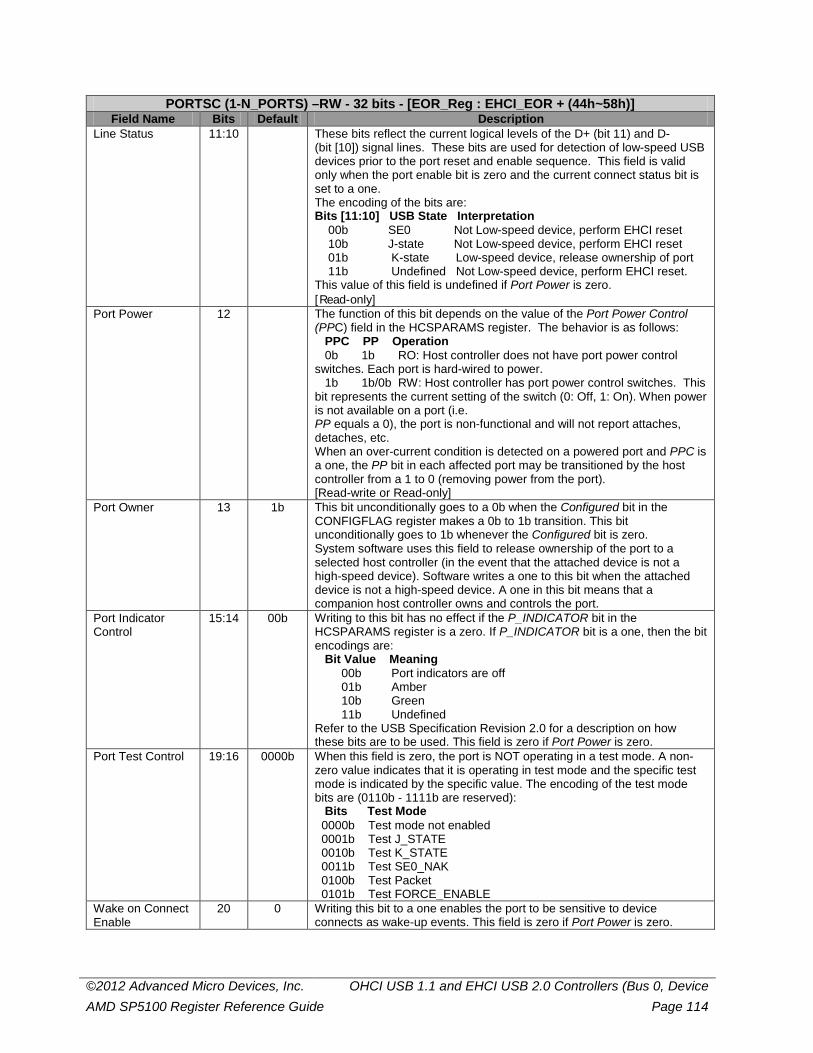
©2012 Advanced Micro Devices, Inc. OHCI USB 1.1 and EHCI USB 2.0 Controllers (Bus 0, Device AMD SP5100 Register Reference Guide Page 114
PORTSC (1-N_PORTS) –RW - 32 bits - [EOR_Reg : EHCI_EOR + (44h~58h)] Field Name Bits Default Description
Line Status 11:10 These bits reflect the current logical levels of the D+ (bit 11) and D- (bit [10]) signal lines. These bits are used for detection of low-speed USB devices prior to the port reset and enable sequence. This field is valid only when the port enable bit is zero and the current connect status bit is set to a one. The encoding of the bits are: Bits [11:10] USB State Interpretation 00b SE0 Not Low-speed device, perform EHCI reset 10b J-state Not Low-speed device, perform EHCI reset 01b K-state Low-speed device, release ownership of port 11b Undefined Not Low-speed device, perform EHCI reset. This value of this field is undefined if Port Power is zero. [Read-only]
Port Power 12 The function of this bit depends on the value of the Port Power Control (PPC) field in the HCSPARAMS register. The behavior is as follows: PPC PP Operation 0b 1b RO: Host controller does not have port power control switches. Each port is hard-wired to power. 1b 1b/0b RW: Host controller has port power control switches. This bit represents the current setting of the switch (0: Off, 1: On). When power is not available on a port (i.e. PP equals a 0), the port is non-functional and will not report attaches, detaches, etc. When an over-current condition is detected on a powered port and PPC is a one, the PP bit in each affected port may be transitioned by the host controller from a 1 to 0 (removing power from the port). [Read-write or Read-only]
Port Owner 13 1b This bit unconditionally goes to a 0b when the Configured bit in the CONFIGFLAG register makes a 0b to 1b transition. This bit unconditionally goes to 1b whenever the Configured bit is zero. System software uses this field to release ownership of the port to a selected host controller (in the event that the attached device is not a high-speed device). Software writes a one to this bit when the attached device is not a high-speed device. A one in this bit means that a companion host controller owns and controls the port.
Port Indicator Control
15:14 00b Writing to this bit has no effect if the P_INDICATOR bit in the HCSPARAMS register is a zero. If P_INDICATOR bit is a one, then the bit encodings are: Bit Value Meaning 00b Port indicators are off 01b Amber 10b Green 11b Undefined Refer to the USB Specification Revision 2.0 for a description on how these bits are to be used. This field is zero if Port Power is zero.
Port Test Control 19:16 0000b When this field is zero, the port is NOT operating in a test mode. A non-zero value indicates that it is operating in test mode and the specific test mode is indicated by the specific value. The encoding of the test mode bits are (0110b - 1111b are reserved): Bits Test Mode 0000b Test mode not enabled 0001b Test J_STATE 0010b Test K_STATE 0011b Test SE0_NAK 0100b Test Packet 0101b Test FORCE_ENABLE
Wake on Connect Enable
20 0 Writing this bit to a one enables the port to be sensitive to device connects as wake-up events. This field is zero if Port Power is zero.
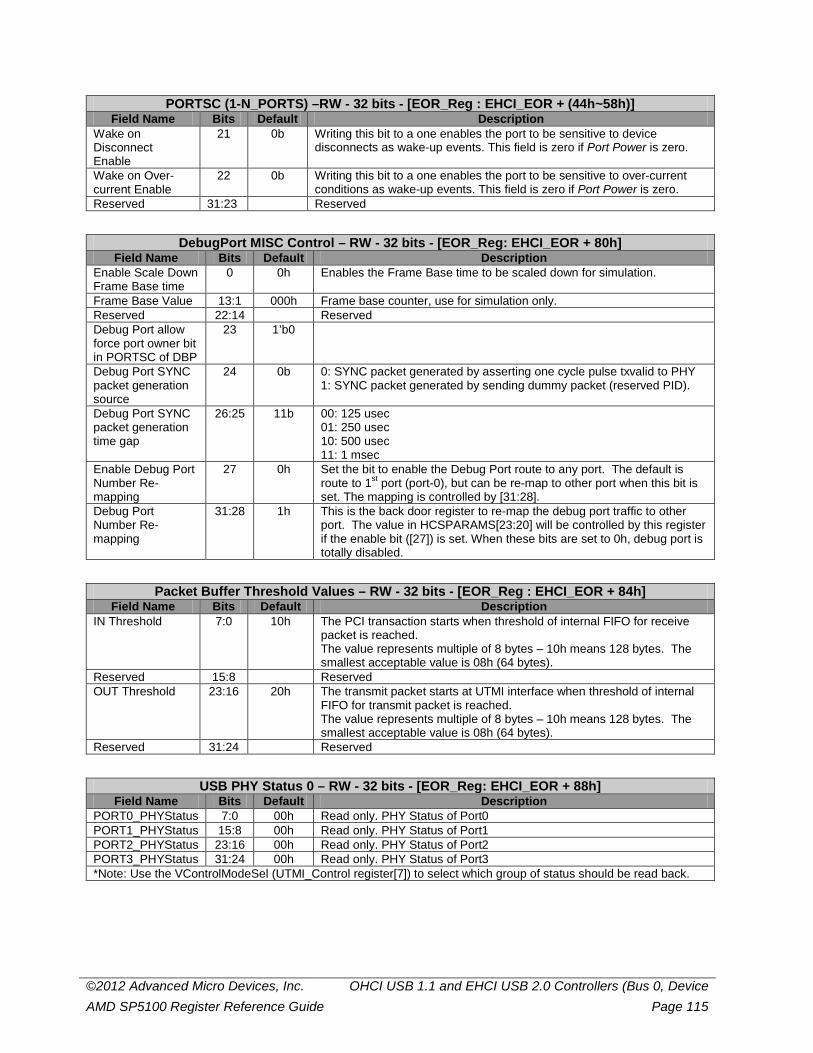
©2012 Advanced Micro Devices, Inc. OHCI USB 1.1 and EHCI USB 2.0 Controllers (Bus 0, Device AMD SP5100 Register Reference Guide Page 115
PORTSC (1-N_PORTS) –RW - 32 bits - [EOR_Reg : EHCI_EOR + (44h~58h)] Field Name Bits Default Description
Wake on Disconnect Enable
21 0b Writing this bit to a one enables the port to be sensitive to device disconnects as wake-up events. This field is zero if Port Power is zero.
Wake on Over-current Enable
22 0b Writing this bit to a one enables the port to be sensitive to over-current conditions as wake-up events. This field is zero if Port Power is zero.
Reserved 31:23 Reserved
DebugPort MISC Control – RW - 32 bits - [EOR_Reg: EHCI_EOR + 80h] Field Name Bits Default Description
Enable Scale Down Frame Base time
0 0h Enables the Frame Base time to be scaled down for simulation.
Frame Base Value 13:1 000h Frame base counter, use for simulation only. Reserved 22:14 Reserved Debug Port allow force port owner bit in PORTSC of DBP
23 1’b0
Debug Port SYNC packet generation source
24 0b 0: SYNC packet generated by asserting one cycle pulse txvalid to PHY 1: SYNC packet generated by sending dummy packet (reserved PID).
Debug Port SYNC packet generation time gap
26:25 11b 00: 125 usec 01: 250 usec 10: 500 usec 11: 1 msec
Enable Debug Port Number Re-mapping
27 0h Set the bit to enable the Debug Port route to any port. The default is route to 1st port (port-0), but can be re-map to other port when this bit is set. The mapping is controlled by [31:28].
Debug Port Number Re-mapping
31:28 1h This is the back door register to re-map the debug port traffic to other port. The value in HCSPARAMS[23:20] will be controlled by this register if the enable bit ([27]) is set. When these bits are set to 0h, debug port is totally disabled.
Packet Buffer Threshold Values – RW - 32 bits - [EOR_Reg : EHCI_EOR + 84h] Field Name Bits Default Description
IN Threshold 7:0 10h The PCI transaction starts when threshold of internal FIFO for receive packet is reached. The value represents multiple of 8 bytes – 10h means 128 bytes. The smallest acceptable value is 08h (64 bytes).
Reserved 15:8 Reserved OUT Threshold 23:16 20h The transmit packet starts at UTMI interface when threshold of internal
FIFO for transmit packet is reached. The value represents multiple of 8 bytes – 10h means 128 bytes. The smallest acceptable value is 08h (64 bytes).
Reserved 31:24 Reserved
USB PHY Status 0 – RW - 32 bits - [EOR_Reg: EHCI_EOR + 88h] Field Name Bits Default Description
PORT0_PHYStatus 7:0 00h Read only. PHY Status of Port0 PORT1_PHYStatus 15:8 00h Read only. PHY Status of Port1 PORT2_PHYStatus 23:16 00h Read only. PHY Status of Port2 PORT3_PHYStatus 31:24 00h Read only. PHY Status of Port3 *Note: Use the VControlModeSel (UTMI_Control register[7]) to select which group of status should be read back.
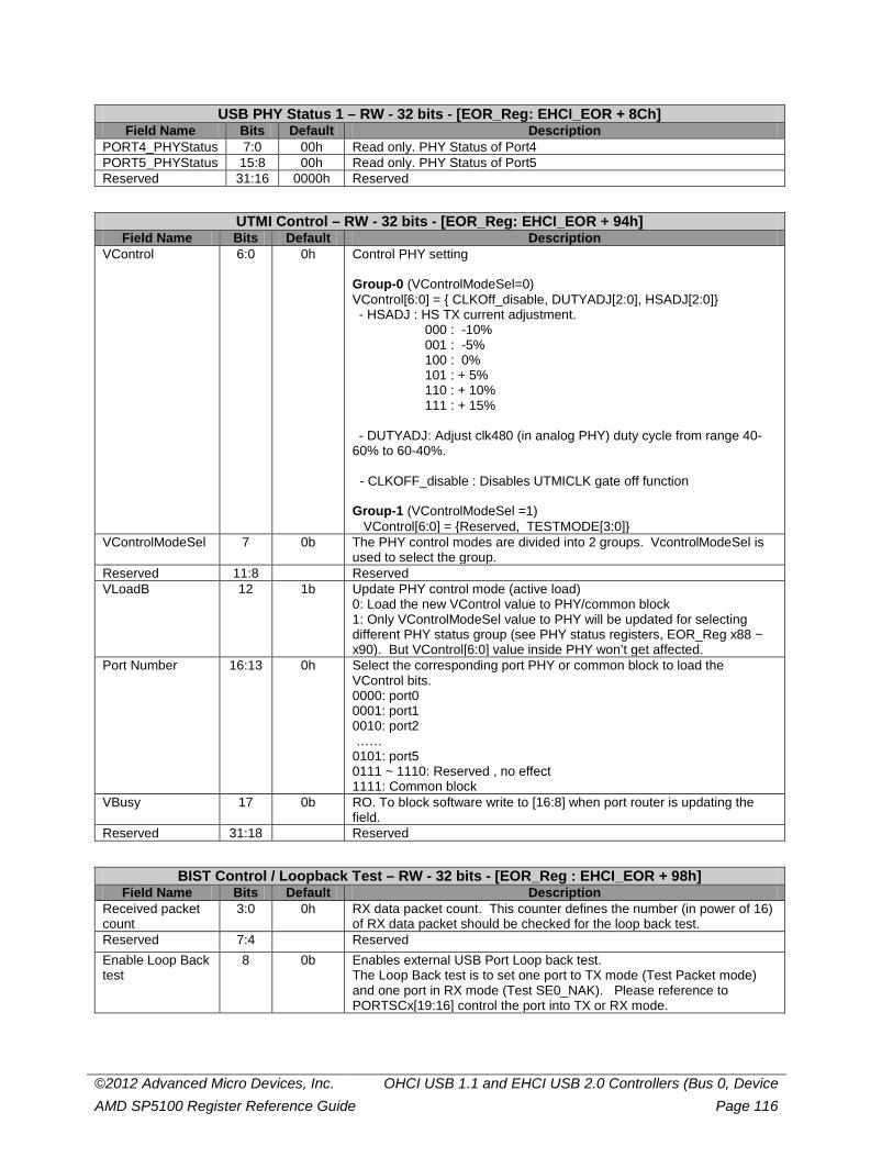
©2012 Advanced Micro Devices, Inc. OHCI USB 1.1 and EHCI USB 2.0 Controllers (Bus 0, Device AMD SP5100 Register Reference Guide Page 116
USB PHY Status 1 – RW - 32 bits - [EOR_Reg: EHCI_EOR + 8Ch] Field Name Bits Default Description
PORT4_PHYStatus 7:0 00h Read only. PHY Status of Port4 PORT5_PHYStatus 15:8 00h Read only. PHY Status of Port5 Reserved 31:16 0000h Reserved
UTMI Control – RW - 32 bits - [EOR_Reg: EHCI_EOR + 94h] Field Name Bits Default Description
VControl 6:0 0h Control PHY setting Group-0 (VControlModeSel=0) VControl[6:0] = { CLKOff_disable, DUTYADJ[2:0], HSADJ[2:0]} - HSADJ : HS TX current adjustment. 000 : -10% 001 : -5% 100 : 0% 101 : + 5% 110 : + 10% 111 : + 15% - DUTYADJ: Adjust clk480 (in analog PHY) duty cycle from range 40-
60% to 60-40%.
- CLKOFF_disable : Disables UTMICLK gate off function Group-1 (VControlModeSel =1) VControl[6:0] = {Reserved, TESTMODE[3:0]}
VControlModeSel 7 0b The PHY control modes are divided into 2 groups. VcontrolModeSel is used to select the group.
Reserved 11:8 Reserved VLoadB 12 1b Update PHY control mode (active load)
0: Load the new VControl value to PHY/common block 1: Only VControlModeSel value to PHY will be updated for selecting different PHY status group (see PHY status registers, EOR_Reg x88 ~ x90). But VControl[6:0] value inside PHY won’t get affected.
Port Number 16:13 0h Select the corresponding port PHY or common block to load the VControl bits. 0000: port0 0001: port1 0010: port2 …… 0101: port5 0111 ~ 1110: Reserved , no effect 1111: Common block
VBusy 17 0b RO. To block software write to [16:8] when port router is updating the field.
Reserved 31:18 Reserved
BIST Control / Loopback Test – RW - 32 bits - [EOR_Reg : EHCI_EOR + 98h] Field Name Bits Default Description
Received packet count
3:0 0h RX data packet count. This counter defines the number (in power of 16) of RX data packet should be checked for the loop back test.
Reserved 7:4 Reserved Enable Loop Back test
8 0b Enables external USB Port Loop back test. The Loop Back test is to set one port to TX mode (Test Packet mode) and one port in RX mode (Test SE0_NAK). Please reference to PORTSCx[19:16] control the port into TX or RX mode.
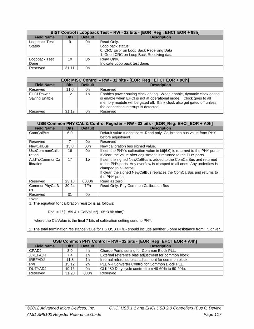
©2012 Advanced Micro Devices, Inc. OHCI USB 1.1 and EHCI USB 2.0 Controllers (Bus 0, Device AMD SP5100 Register Reference Guide Page 117
BIST Control / Loopback Test – RW - 32 bits - [EOR_Reg : EHCI_EOR + 98h] Field Name Bits Default Description
Loopback Test Status
9 0b Read Only. Loop back status. 0: CRC Error on Loop Back Receiving Data 1: Good CRC on Loop Back Receiving data
Loopback Test Done
10 0b Read Only. Indicate Loop back test done.
Reserved 31:11 0h
EOR MISC Control – RW - 32 bits - [EOR_Reg : EHCI_EOR + 9Ch] Field Name Bits Default Description
Reserved 11:0 0h Reserved EHCI Power Saving Enable
12 1b Enables power saving clock gating. When enable, dynamic clock gating is enable when EHCI is not at operational mode. Clock goes to all memory module will be gated off, Blink clock also got gated off unless the connection interrupt is detected.
Reserved 31:13 0h Reserved
USB Common PHY CAL & Control Register – RW - 32 bits - [EOR_Reg: EHCI_EOR + A0h] Field Name Bits Default Description
ComCalBus 6:0 Default value = don’t care. Read only. Calibration bus value from PHY before adjustment.
Reserved 7 0b Reserved NewCalBus 15:8 00h New calibration bus signed value. UseCommonCalibration
16 0b
If set, the PHY’s calibration value in bit[6:0] is returned to the PHY ports. If clear, the value after adjustment is returned to the PHY ports.
AddToCommonCalibration
17 1b If set, the signed NewCalBus is added to the ComCalBus and returned to the PHY ports. Any overflow is clamped to all ones. Any underflow is clamped to all zeros. If clear, the signed NewCalBus replaces the ComCalBus and returns to the PHY ports.
Reserved 23:18 0000h Read as zero. CommonPhyCalBus
30:24 7Fh Read Only. Phy Common Calibration Bus
Reserved 31 0b *Note: 1. The equation for calibration resistor is as follows: Rcal = 1/ [ 1/59.4 + CalValue/(1.05*3.8k ohm)] where the CalValue is the final 7 bits of calibration setting send to PHY. 2. The total termination resistance value for HS USB D+/D- should include another 5 ohm resistance from FS driver.
USB Common PHY Control – RW - 32 bits - [EOR_Reg: EHCI_EOR + A4h] Field Name Bits Default Description
CPADJ 3:0 4h Charge Pump setting for Common Block PLL. XREFADJ 7:4 1h External reference bias adjustment for common block. IREFADJ 11:8 1h Internal reference bias adjustment for common block. PVI 15:12 2h PLL V-I Converter Control for Common Block PLL. DUTYADJ 19:16 0h CLK480 Duty cycle control from 40-60% to 60-40%. Reserved 31:20 000h Reserved
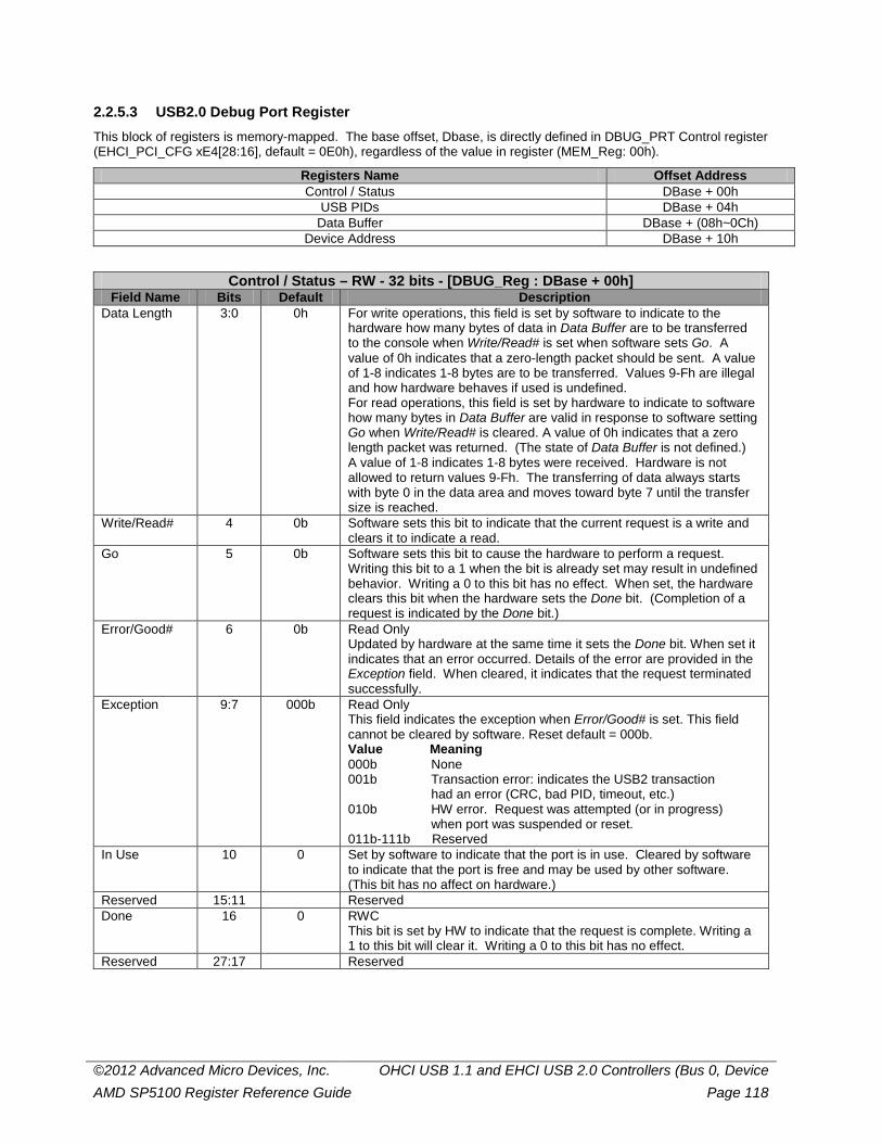
©2012 Advanced Micro Devices, Inc. OHCI USB 1.1 and EHCI USB 2.0 Controllers (Bus 0, Device AMD SP5100 Register Reference Guide Page 118
2.2.5.3 USB2.0 Debug Port Register This block of registers is memory-mapped. The base offset, Dbase, is directly defined in DBUG_PRT Control register (EHCI_PCI_CFG xE4[28:16], default = 0E0h), regardless of the value in register (MEM_Reg: 00h).
Registers Name Offset Address Control / Status DBase + 00h
USB PIDs DBase + 04h Data Buffer DBase + (08h~0Ch)
Device Address DBase + 10h
Control / Status – RW - 32 bits - [DBUG_Reg : DBase + 00h] Field Name Bits Default Description
Data Length 3:0 0h For write operations, this field is set by software to indicate to the hardware how many bytes of data in Data Buffer are to be transferred to the console when Write/Read# is set when software sets Go. A value of 0h indicates that a zero-length packet should be sent. A value of 1-8 indicates 1-8 bytes are to be transferred. Values 9-Fh are illegal and how hardware behaves if used is undefined. For read operations, this field is set by hardware to indicate to software how many bytes in Data Buffer are valid in response to software setting Go when Write/Read# is cleared. A value of 0h indicates that a zero length packet was returned. (The state of Data Buffer is not defined.) A value of 1-8 indicates 1-8 bytes were received. Hardware is not allowed to return values 9-Fh. The transferring of data always starts with byte 0 in the data area and moves toward byte 7 until the transfer size is reached.
Write/Read# 4 0b Software sets this bit to indicate that the current request is a write and clears it to indicate a read.
Go 5 0b Software sets this bit to cause the hardware to perform a request. Writing this bit to a 1 when the bit is already set may result in undefined behavior. Writing a 0 to this bit has no effect. When set, the hardware clears this bit when the hardware sets the Done bit. (Completion of a request is indicated by the Done bit.)
Error/Good# 6 0b Read Only Updated by hardware at the same time it sets the Done bit. When set it indicates that an error occurred. Details of the error are provided in the Exception field. When cleared, it indicates that the request terminated successfully.
Exception 9:7 000b Read Only This field indicates the exception when Error/Good# is set. This field cannot be cleared by software. Reset default = 000b. Value Meaning 000b None 001b Transaction error: indicates the USB2 transaction had an error (CRC, bad PID, timeout, etc.) 010b HW error. Request was attempted (or in progress) when port was suspended or reset. 011b-111b Reserved
In Use 10 0 Set by software to indicate that the port is in use. Cleared by software to indicate that the port is free and may be used by other software. (This bit has no affect on hardware.)
Reserved 15:11 Reserved Done 16 0 RWC
This bit is set by HW to indicate that the request is complete. Writing a 1 to this bit will clear it. Writing a 0 to this bit has no effect.
Reserved 27:17 Reserved
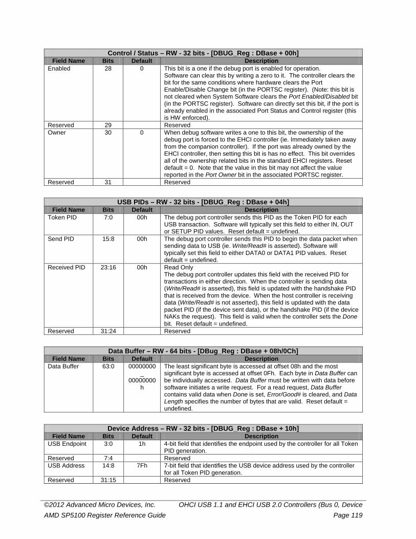
©2012 Advanced Micro Devices, Inc. OHCI USB 1.1 and EHCI USB 2.0 Controllers (Bus 0, Device AMD SP5100 Register Reference Guide Page 119
Control / Status – RW - 32 bits - [DBUG_Reg : DBase + 00h] Field Name Bits Default Description
Enabled 28 0 This bit is a one if the debug port is enabled for operation. Software can clear this by writing a zero to it. The controller clears the bit for the same conditions where hardware clears the Port Enable/Disable Change bit (in the PORTSC register). (Note: this bit is not cleared when System Software clears the Port Enabled/Disabled bit (in the PORTSC register). Software can directly set this bit, if the port is already enabled in the associated Port Status and Control register (this is HW enforced).
Reserved 29 Reserved Owner 30 0 When debug software writes a one to this bit, the ownership of the
debug port is forced to the EHCI controller (ie. Immediately taken away from the companion controller). If the port was already owned by the EHCI controller, then setting this bit is has no effect. This bit overrides all of the ownership related bits in the standard EHCI registers. Reset default = 0. Note that the value in this bit may not affect the value reported in the Port Owner bit in the associated PORTSC register.
Reserved 31 Reserved
USB PIDs – RW - 32 bits - [DBUG_Reg : DBase + 04h] Field Name Bits Default Description
Token PID 7:0 00h The debug port controller sends this PID as the Token PID for each USB transaction. Software will typically set this field to either IN, OUT or SETUP PID values. Reset default = undefined.
Send PID 15:8 00h The debug port controller sends this PID to begin the data packet when sending data to USB (ie. Write/Read# is asserted). Software will typically set this field to either DATA0 or DATA1 PID values. Reset default = undefined.
Received PID 23:16 00h Read Only The debug port controller updates this field with the received PID for transactions in either direction. When the controller is sending data (Write/Read# is asserted), this field is updated with the handshake PID that is received from the device. When the host controller is receiving data (Write/Read# is not asserted), this field is updated with the data packet PID (if the device sent data), or the handshake PID (if the device NAKs the request). This field is valid when the controller sets the Done bit. Reset default = undefined.
Reserved 31:24 Reserved
Data Buffer – RW - 64 bits - [DBug_Reg : DBase + 08h/0Ch] Field Name Bits Default Description
Data Buffer 63:0 00000000_
00000000h
The least significant byte is accessed at offset 08h and the most significant byte is accessed at offset 0Fh. Each byte in Data Buffer can be individually accessed. Data Buffer must be written with data before software initiates a write request. For a read request, Data Buffer contains valid data when Done is set, Error/Good# is cleared, and Data Length specifies the number of bytes that are valid. Reset default = undefined.
Device Address – RW - 32 bits - [DBUG_Reg : DBase + 10h] Field Name Bits Default Description
USB Endpoint 3:0 1h 4-bit field that identifies the endpoint used by the controller for all Token PID generation.
Reserved 7:4 Reserved USB Address 14:8 7Fh 7-bit field that identifies the USB device address used by the controller
for all Token PID generation. Reserved 31:15 Reserved
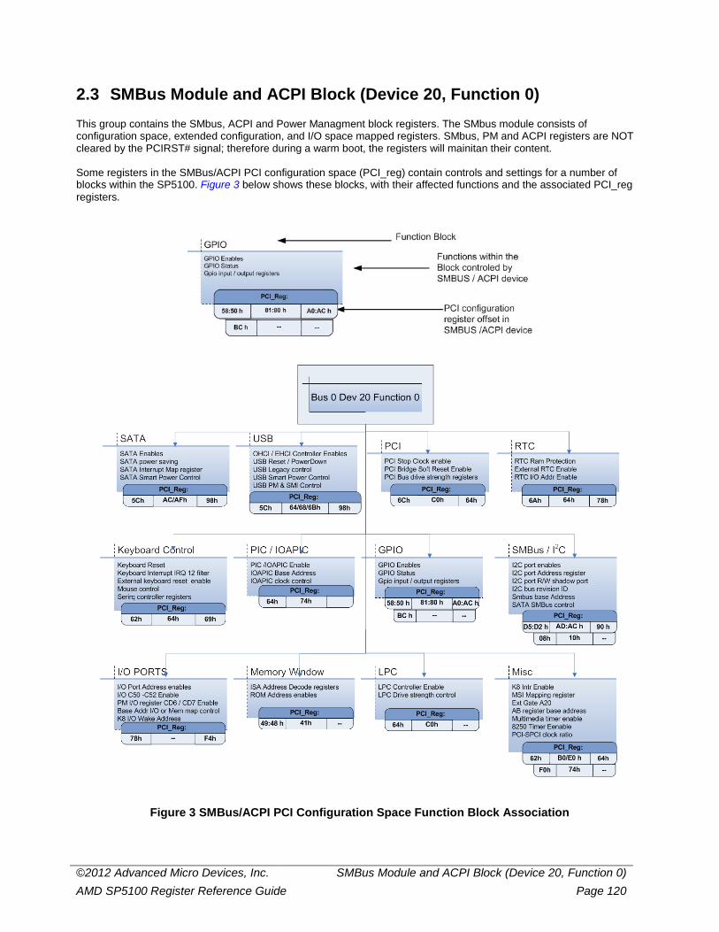
©2012 Advanced Micro Devices, Inc. SMBus Module and ACPI Block (Device 20, Function 0) AMD SP5100 Register Reference Guide Page 120
2.3 SMBus Module and ACPI Block (Device 20, Function 0) This group contains the SMbus, ACPI and Power Managment block registers. The SMbus module consists of configuration space, extended configuration, and I/O space mapped registers. SMbus, PM and ACPI registers are NOT cleared by the PCIRST# signal; therefore during a warm boot, the registers will mainitan their content. Some registers in the SMBus/ACPI PCI configuration space (PCI_reg) contain controls and settings for a number of blocks within the SP5100. Figure 3 below shows these blocks, with their affected functions and the associated PCI_reg registers.
Figure 3 SMBus/ACPI PCI Configuration Space Function Block Association
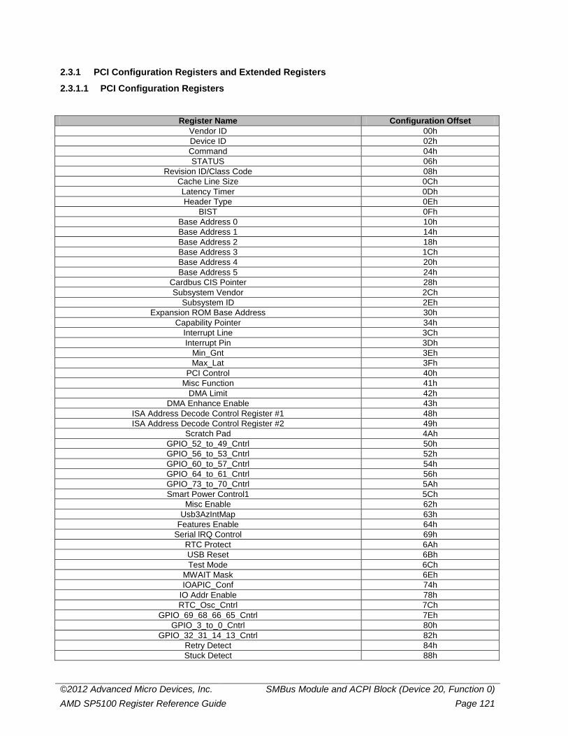
©2012 Advanced Micro Devices, Inc. SMBus Module and ACPI Block (Device 20, Function 0) AMD SP5100 Register Reference Guide Page 121
2.3.1 PCI Configuration Registers and Extended Registers
2.3.1.1 PCI Configuration Registers
Register Name Configuration Offset Vendor ID 00h Device ID 02h Command 04h STATUS 06h
Revision ID/Class Code 08h Cache Line Size 0Ch Latency Timer 0Dh Header Type 0Eh
BIST 0Fh Base Address 0 10h Base Address 1 14h Base Address 2 18h Base Address 3 1Ch Base Address 4 20h Base Address 5 24h
Cardbus CIS Pointer 28h Subsystem Vendor 2Ch
Subsystem ID 2Eh Expansion ROM Base Address 30h
Capability Pointer 34h Interrupt Line 3Ch Interrupt Pin 3Dh
Min_Gnt 3Eh Max_Lat 3Fh
PCI Control 40h Misc Function 41h
DMA Limit 42h DMA Enhance Enable 43h
ISA Address Decode Control Register #1 48h ISA Address Decode Control Register #2 49h
Scratch Pad 4Ah GPIO_52_to_49_Cntrl 50h GPIO_56_to_53_Cntrl 52h GPIO_60_to_57_Cntrl 54h GPIO_64_to_61_Cntrl 56h GPIO_73_to_70_Cntrl 5Ah Smart Power Control1 5Ch
Misc Enable 62h Usb3AzIntMap 63h
Features Enable 64h Serial lRQ Control 69h
RTC Protect 6Ah USB Reset 6Bh Test Mode 6Ch
MWAIT Mask 6Eh IOAPIC_Conf 74h
IO Addr Enable 78h RTC_Osc_Cntrl 7Ch
GPIO_69_68_66_65_Cntrl 7Eh GPIO_3_to_0_Cntrl 80h
GPIO_32_31_14_13_Cntrl 82h Retry Detect 84h Stuck Detect 88h

©2012 Advanced Micro Devices, Inc. SMBus Module and ACPI Block (Device 20, Function 0) AMD SP5100 Register Reference Guide Page 122
Register Name Configuration Offset BIOS RAM Base Addr 8Ch Smbus Base Address 90h
Serial IRQ Status 94h Smart Power Control2 98h
PM_IO Base Addr 9Ch IDE_GPIO_Cntrl A0h
IDE_GPIO_In A4h GPIO_48_47_46_37_Cntrl A6h
GPIO_12_to_4_Cntrl A8h SATA_ACT_GPIO_Cntrl ACh
SATA Enable ADh Misc Control AEh SataIntMap AFh
MSI Mapping Capability B0h PCI_INT_GPIO_Cntrl BCh
UsbIntMap BEh IO Drive Strength C0h
I2CbusConfig D2h I2CCommand D3h I2CShadow1 D4h I2Cshadow2 D5h
I2CBusRevision D6h MSI Weight E0h
MiscE1 E1h AB_REG_BAR F0h Wake IO Addr F4h
MWAIT ID F6h MWAIT Status F7h
Extended Addr Port F8h Extended Data Port FCh
VendorID - R - 16 bits - [PCI_Reg: 00h] Field Name Bits Default Description
VendorID 15:0 1002h Vendor ID Vendor ID register: Vendor Identification
DeviceID - R - 16 bits - [PCI_Reg: 02h] Field Name Bits Default Description
DeviceID 31:16 4385h Device ID Device ID register: Device Identification Number
Command- RW - 16 bits - [PCI_Reg: 04h] Field Name Bits Default Description
I/O Space 0 1b This bit controls a device’s response to IO space accesses. A value of 1 enables it and a value of 0 disables it. Since this module does claim certain legacy IO cycles, this bit is default to 1.
Memory Space 1 1b This bit controls a device’s response to memory space accesses. A value of 1 enables it and a value of 0 disables it. Since this module does claim certain memory cycles if BIOS is strapped to the PCI bus, this bit is default to 1.
Bus Master 2 0b A value of 0 disables the device from generating PCI accesses. A value of 1 allows it to behave as a bus master. ACPI/SMBus does not have PCI master and so it is always 0. [Read-only]
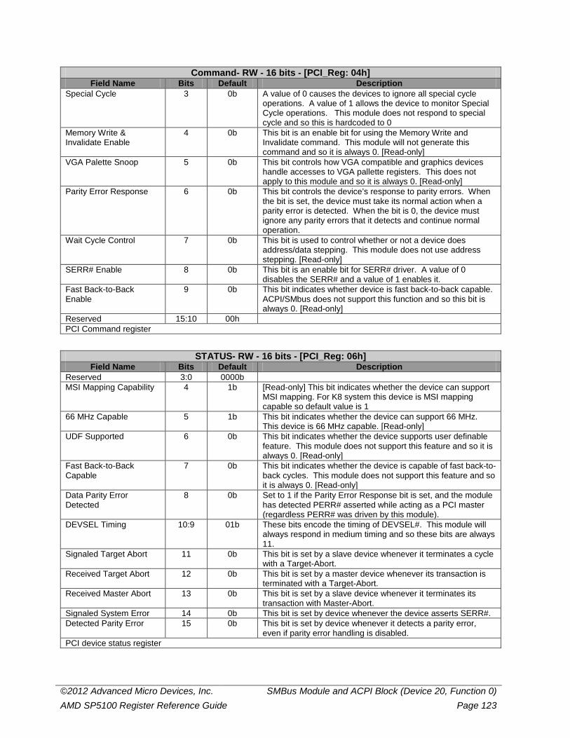
©2012 Advanced Micro Devices, Inc. SMBus Module and ACPI Block (Device 20, Function 0) AMD SP5100 Register Reference Guide Page 123
Command- RW - 16 bits - [PCI_Reg: 04h] Field Name Bits Default Description
Special Cycle 3 0b A value of 0 causes the devices to ignore all special cycle operations. A value of 1 allows the device to monitor Special Cycle operations. This module does not respond to special cycle and so this is hardcoded to 0
Memory Write & Invalidate Enable
4 0b This bit is an enable bit for using the Memory Write and Invalidate command. This module will not generate this command and so it is always 0. [Read-only]
VGA Palette Snoop 5 0b This bit controls how VGA compatible and graphics devices handle accesses to VGA pallette registers. This does not apply to this module and so it is always 0. [Read-only]
Parity Error Response 6 0b This bit controls the device’s response to parity errors. When the bit is set, the device must take its normal action when a parity error is detected. When the bit is 0, the device must ignore any parity errors that it detects and continue normal operation.
Wait Cycle Control 7 0b This bit is used to control whether or not a device does address/data stepping. This module does not use address stepping. [Read-only]
SERR# Enable 8 0b This bit is an enable bit for SERR# driver. A value of 0 disables the SERR# and a value of 1 enables it.
Fast Back-to-Back Enable
9 0b This bit indicates whether device is fast back-to-back capable. ACPI/SMbus does not support this function and so this bit is always 0. [Read-only]
Reserved 15:10 00h PCI Command register
STATUS- RW - 16 bits - [PCI_Reg: 06h] Field Name Bits Default Description
Reserved 3:0 0000b MSI Mapping Capability 4 1b [Read-only] This bit indicates whether the device can support
MSI mapping. For K8 system this device is MSI mapping capable so default value is 1
66 MHz Capable 5 1b This bit indicates whether the device can support 66 MHz. This device is 66 MHz capable. [Read-only]
UDF Supported 6 0b This bit indicates whether the device supports user definable feature. This module does not support this feature and so it is always 0. [Read-only]
Fast Back-to-Back Capable
7 0b This bit indicates whether the device is capable of fast back-to-back cycles. This module does not support this feature and so it is always 0. [Read-only]
Data Parity Error Detected
8 0b Set to 1 if the Parity Error Response bit is set, and the module has detected PERR# asserted while acting as a PCI master (regardless PERR# was driven by this module).
DEVSEL Timing 10:9 01b These bits encode the timing of DEVSEL#. This module will always respond in medium timing and so these bits are always 11.
Signaled Target Abort 11 0b This bit is set by a slave device whenever it terminates a cycle with a Target-Abort.
Received Target Abort 12 0b This bit is set by a master device whenever its transaction is terminated with a Target-Abort.
Received Master Abort 13 0b This bit is set by a slave device whenever it terminates its transaction with Master-Abort.
Signaled System Error 14 0b This bit is set by device whenever the device asserts SERR#. Detected Parity Error 15 0b This bit is set by device whenever it detects a parity error,
even if parity error handling is disabled. PCI device status register
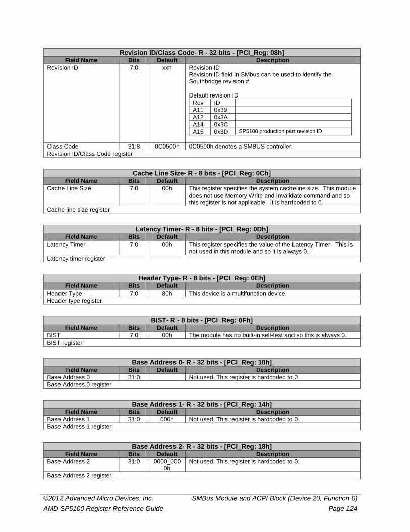
©2012 Advanced Micro Devices, Inc. SMBus Module and ACPI Block (Device 20, Function 0) AMD SP5100 Register Reference Guide Page 124
Revision ID/Class Code- R - 32 bits - [PCI_Reg: 08h] Field Name Bits Default Description
Revision ID 7:0 xxh Revision ID Revision ID field in SMbus can be used to identify the Southbridge revision #. Default revision ID
Rev ID A11 0x39 A12 0x3A A14 0x3C A15 0x3D SP5100 production part revision ID
Class Code 31:8 0C0500h 0C0500h denotes a SMBUS controller. Revision ID/Class Code register
Cache Line Size- R - 8 bits - [PCI_Reg: 0Ch] Field Name Bits Default Description
Cache Line Size 7:0 00h This register specifies the system cacheline size. This module does not use Memory Write and Invalidate command and so this register is not applicable. It is hardcoded to 0.
Cache line size register
Latency Timer- R - 8 bits - [PCI_Reg: 0Dh] Field Name Bits Default Description
Latency Timer 7:0 00h This register specifies the value of the Latency Timer. This is not used in this module and so it is always 0.
Latency timer register
Header Type- R - 8 bits - [PCI_Reg: 0Eh] Field Name Bits Default Description
Header Type 7:0 80h This device is a multifunction device. Header type register
BIST- R - 8 bits - [PCI_Reg: 0Fh] Field Name Bits Default Description
BIST 7:0 00h The module has no built-in self-test and so this is always 0. BIST register
Base Address 0- R - 32 bits - [PCI_Reg: 10h] Field Name Bits Default Description
Base Address 0 31:0 Not used. This register is hardcoded to 0. Base Address 0 register
Base Address 1- R - 32 bits - [PCI_Reg: 14h] Field Name Bits Default Description
Base Address 1 31:0 000h Not used. This register is hardcoded to 0. Base Address 1 register
Base Address 2- R - 32 bits - [PCI_Reg: 18h] Field Name Bits Default Description
Base Address 2 31:0 0000_0000h
Not used. This register is hardcoded to 0.
Base Address 2 register

©2012 Advanced Micro Devices, Inc. SMBus Module and ACPI Block (Device 20, Function 0) AMD SP5100 Register Reference Guide Page 125
Base Address 3- R - 32 bits - [PCI_Reg: 1Ch] Field Name Bits Default Description
Base Address 3 31:0 0000_0000h
Not used. This register is hardcoded to 0.
Base Address 3 register
Base Address 4- R - 32 bits - [PCI_Reg: 20h] Field Name Bits Default Description
Base Address 4 31:0 0000_0000h
Not used. This register is hardcoded to 0.
Base Address 4 register
Base Address 5- R - 32 bits - [PCI_Reg: 24h] Field Name Bits Default Description
Base Address 5 31:0 0000_0000h
Not used. This register is hardcoded to 0.
Base Address 5 register
Cardbus CIS Pointer- R - 32 bits - [PCI_Reg: 28h] Field Name Bits Default Description
Cardbus CIS Pointer 31:0 0000_0000h
Not used. This register is hardcoded to 0.
Cardbus CIS Pointer register
Subsystem Vendor ID- W - 16 bits - [PCI_Reg: 2Ch] Field Name Bits Default Description
Subsystem Vendor ID 15:0 0000h Write once. Subsystem Vendor ID register
Subsystem ID- W - 16 bits - [PCI_Reg: 2Eh] Field Name Bits Default Description
Subsystem ID 15:0 0000h Write once. Subsystem ID register
Expansion ROM Base Address - R - 8 bits - [PCI_Reg: 30h] Field Name Bits Default Description
Expansion ROM Base Address
7:0 00h Not used. This register is hardcoded to 0.
Expansion ROM Base Address register
Capability Pointer - R - 8 bits - [PCI_Reg: 34h] Field Name Bits Default Description
Capability Pointer 7:0 B0 Default value is B0h Capability Pointer register Definition of this register applies to Revision A14 and above when the reference clock source is from an external 14 MHz external crystal. The default selection for Revision A14 and above is to use a 14-MHz external crystal, which is initialized by BIOS on POST. Refer to the definition of register PM 0xD4, field AltClk14En, for information on how the reference clock source is selected.
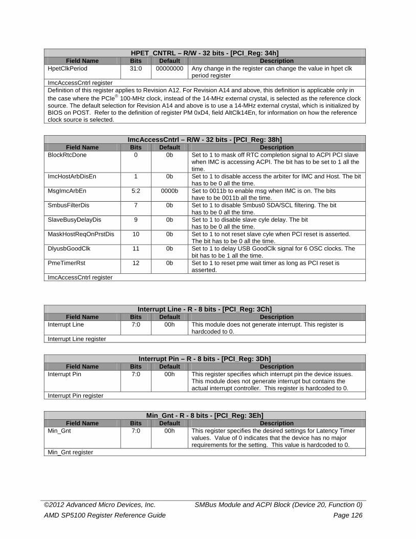
©2012 Advanced Micro Devices, Inc. SMBus Module and ACPI Block (Device 20, Function 0) AMD SP5100 Register Reference Guide Page 126
HPET_CNTRL – R/W - 32 bits - [PCI_Reg: 34h] Field Name Bits Default Description
HpetClkPeriod 31:0 00000000 Any change in the register can change the value in hpet clk period register
ImcAccessCntrl register Definition of this register applies to Revision A12. For Revision A14 and above, this definition is applicable only in the case where the PCIe 100-MHz clock, instead of the 14-MHz external crystal, is selected as the reference clock source. The default selection for Revision A14 and above is to use a 14-MHz external crystal, which is initialized by BIOS on POST. Refer to the definition of register PM 0xD4, field AltClk14En, for information on how the reference clock source is selected.
ImcAccessCntrl – R/W - 32 bits - [PCI_Reg: 38h] Field Name Bits Default Description
BlockRtcDone 0 0b Set to 1 to mask off RTC completion signal to ACPI PCI slave when IMC is accessing ACPI. The bit has to be set to 1 all the time.
ImcHostArbDisEn 1 0b Set to 1 to disable access the arbiter for IMC and Host. The bit has to be 0 all the time.
MsgImcArbEn 5:2 0000b Set to 0011b to enable msg when IMC is on. The bits have to be 0011b all the time.
SmbusFilterDis 7 0b Set to 1 to disable Smbus0 SDA/SCL filtering. The bit has to be 0 all the time.
SlaveBusyDelayDis 9 0b Set to 1 to disable slave cyle delay. The bit has to be 0 all the time.
MaskHostReqOnPrstDis 10 0b Set to 1 to not reset slave cyle when PCI reset is asserted. The bit has to be 0 all the time.
DlyusbGoodClk 11 0b Set to 1 to delay USB GoodClk signal for 6 OSC clocks. The bit has to be 1 all the time.
PmeTimerRst 12 0b Set to 1 to reset pme wait timer as long as PCI reset is asserted.
ImcAccessCntrl register
Interrupt Line - R - 8 bits - [PCI_Reg: 3Ch] Field Name Bits Default Description
Interrupt Line 7:0 00h This module does not generate interrupt. This register is hardcoded to 0.
Interrupt Line register
Interrupt Pin – R - 8 bits - [PCI_Reg: 3Dh] Field Name Bits Default Description
Interrupt Pin 7:0 00h This register specifies which interrupt pin the device issues. This module does not generate interrupt but contains the actual interrupt controller. This register is hardcoded to 0.
Interrupt Pin register
Min_Gnt - R - 8 bits - [PCI_Reg: 3Eh] Field Name Bits Default Description
Min_Gnt 7:0 00h This register specifies the desired settings for Latency Timer values. Value of 0 indicates that the device has no major requirements for the setting. This value is hardcoded to 0.
Min_Gnt register
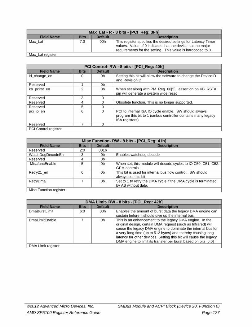
©2012 Advanced Micro Devices, Inc. SMBus Module and ACPI Block (Device 20, Function 0) AMD SP5100 Register Reference Guide Page 127
Max_Lat - R - 8 bits - [PCI_Reg: 3Fh] Field Name Bits Default Description
Max_Lat 7:0 00h This register specifies the desired settings for Latency Timer values. Value of 0 indicates that the device has no major requirements for the setting. This value is hardcoded to 0.
Max_Lat register
PCI Control- RW - 8 bits - [PCI_Reg: 40h] Field Name Bits Default Description
id_change_en 0 0b Setting this bit will allow the software to change the DeviceID and RevisionID
Reserved 1 0b kb_pcirst_en 2 0b When set along with PM_Reg_66[5], assertion on KB_RST#
pin will generate a system wide reset Reserved 3 0 Reserved 4 0 Obsolete function. This is no longer supported. Reserved 5 0 pci_io_en 6 0 PCI to internal ISA IO cycle enable. SW should always
program this bit to 1 (smbus controller contains many legacy ISA registers)
Reserved 7 0 PCI Control register
Misc Function- RW - 8 bits - [PCI_Reg: 41h] Field Name Bits Default Description
Reserved 2:0 001b WatchDogDecodeEn 3 0b Enables watchdog decode Reserved 4 0b MiscfuncEnable 5 0b When set, this module will decode cycles to IO C50, C51, C52:
GPM controls. Retry21_en 6 0b This bit is used for internal bus flow control. SW should
always set this bit RetryDma 7 0b Set to 1 to retry the DMA cycle if the DMA cycle is terminated
by AB without data. Misc Function register
DMA Limit- RW - 8 bits - [PCI_Reg: 42h] Field Name Bits Default Description
DmaBurstLimit 6:0 00h Enables the amount of burst data the legacy DMA engine can sustain before it should give up the internal bus.
DmaLimitEnable 7 0h This is an enhancement to the legacy DMA engine. In the original design, certain DMA request (such as Infrared) will cause the legacy DMA engine to dominate the internal bus for a very long time (up to 512 bytes) and thereby causing long latency for other devices. Setting this bit will cause the legacy DMA engine to limit its transfer per burst based on bits [6:0]
DMA Limit register
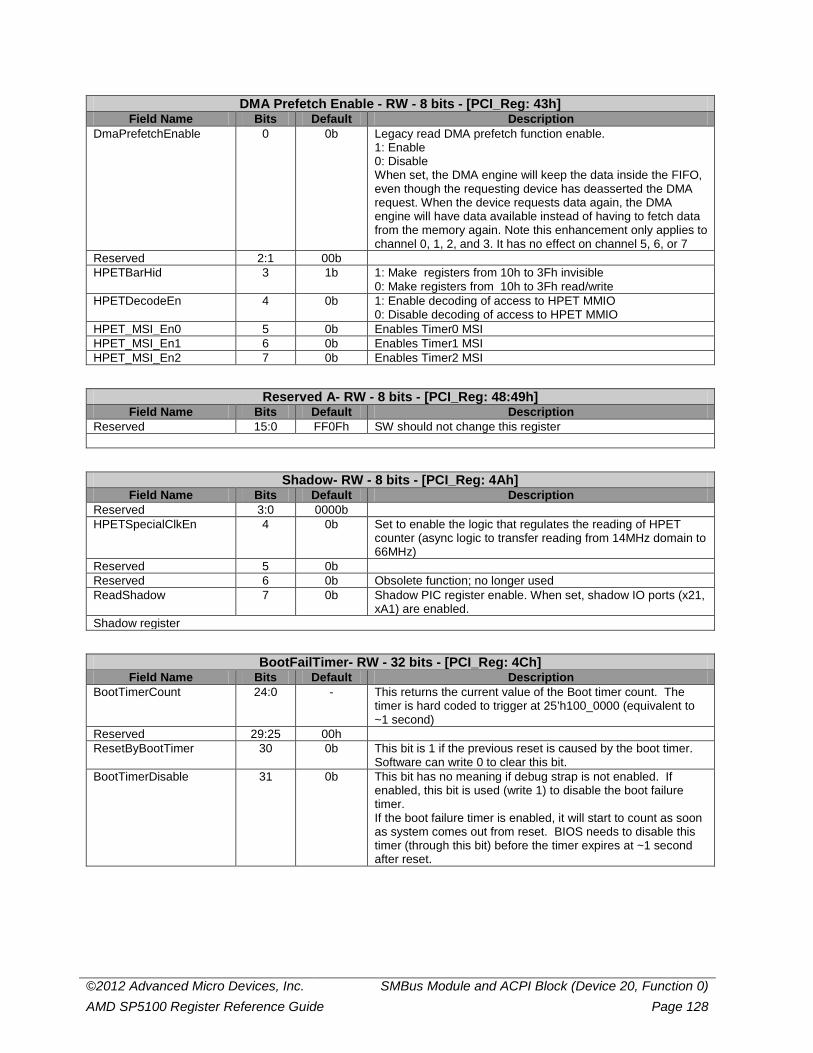
©2012 Advanced Micro Devices, Inc. SMBus Module and ACPI Block (Device 20, Function 0) AMD SP5100 Register Reference Guide Page 128
DMA Prefetch Enable - RW - 8 bits - [PCI_Reg: 43h] Field Name Bits Default Description
DmaPrefetchEnable 0 0b Legacy read DMA prefetch function enable. 1: Enable 0: Disable When set, the DMA engine will keep the data inside the FIFO, even though the requesting device has deasserted the DMA request. When the device requests data again, the DMA engine will have data available instead of having to fetch data from the memory again. Note this enhancement only applies to channel 0, 1, 2, and 3. It has no effect on channel 5, 6, or 7
Reserved 2:1 00b HPETBarHid 3 1b 1: Make registers from 10h to 3Fh invisible
0: Make registers from 10h to 3Fh read/write HPETDecodeEn 4 0b 1: Enable decoding of access to HPET MMIO
0: Disable decoding of access to HPET MMIO HPET_MSI_En0 5 0b Enables Timer0 MSI HPET_MSI_En1 6 0b Enables Timer1 MSI HPET_MSI_En2 7 0b Enables Timer2 MSI
Reserved A- RW - 8 bits - [PCI_Reg: 48:49h] Field Name Bits Default Description
Reserved 15:0 FF0Fh SW should not change this register
Shadow- RW - 8 bits - [PCI_Reg: 4Ah] Field Name Bits Default Description
Reserved 3:0 0000b HPETSpecialClkEn 4 0b Set to enable the logic that regulates the reading of HPET
counter (async logic to transfer reading from 14MHz domain to 66MHz)
Reserved 5 0b Reserved 6 0b Obsolete function; no longer used ReadShadow 7 0b Shadow PIC register enable. When set, shadow IO ports (x21,
xA1) are enabled. Shadow register
BootFailTimer- RW - 32 bits - [PCI_Reg: 4Ch] Field Name Bits Default Description
BootTimerCount 24:0 - This returns the current value of the Boot timer count. The timer is hard coded to trigger at 25’h100_0000 (equivalent to ~1 second)
Reserved 29:25 00h ResetByBootTimer 30 0b This bit is 1 if the previous reset is caused by the boot timer.
Software can write 0 to clear this bit. BootTimerDisable 31 0b This bit has no meaning if debug strap is not enabled. If
enabled, this bit is used (write 1) to disable the boot failure timer. If the boot failure timer is enabled, it will start to count as soon as system comes out from reset. BIOS needs to disable this timer (through this bit) before the timer expires at ~1 second after reset.
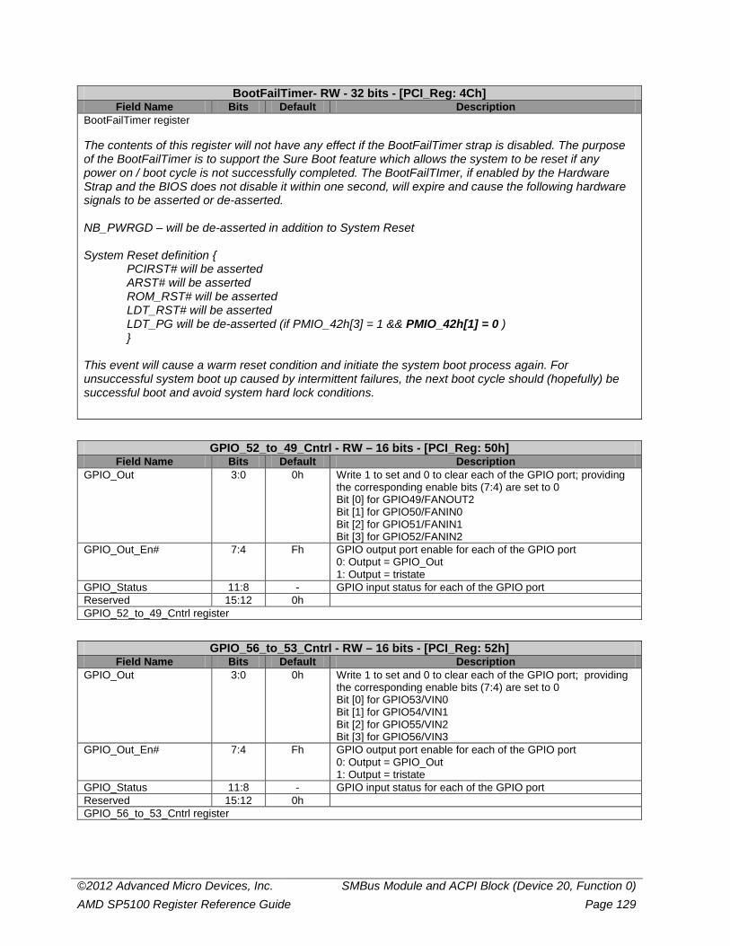
©2012 Advanced Micro Devices, Inc. SMBus Module and ACPI Block (Device 20, Function 0) AMD SP5100 Register Reference Guide Page 129
BootFailTimer- RW - 32 bits - [PCI_Reg: 4Ch] Field Name Bits Default Description
BootFailTimer register The contents of this register will not have any effect if the BootFailTimer strap is disabled. The purpose of the BootFailTimer is to support the Sure Boot feature which allows the system to be reset if any power on / boot cycle is not successfully completed. The BootFailTImer, if enabled by the Hardware Strap and the BIOS does not disable it within one second, will expire and cause the following hardware signals to be asserted or de-asserted. NB_PWRGD – will be de-asserted in addition to System Reset System Reset definition {
PCIRST# will be asserted ARST# will be asserted ROM_RST# will be asserted LDT_RST# will be asserted LDT_PG will be de-asserted (if PMIO_42h[3] = 1 && PMIO_42h[1] = 0 ) }
This event will cause a warm reset condition and initiate the system boot process again. For unsuccessful system boot up caused by intermittent failures, the next boot cycle should (hopefully) be successful boot and avoid system hard lock conditions.
GPIO_52_to_49_Cntrl - RW – 16 bits - [PCI_Reg: 50h] Field Name Bits Default Description
GPIO_Out 3:0 0h Write 1 to set and 0 to clear each of the GPIO port; providing the corresponding enable bits (7:4) are set to 0 Bit [0] for GPIO49/FANOUT2 Bit [1] for GPIO50/FANIN0 Bit [2] for GPIO51/FANIN1 Bit [3] for GPIO52/FANIN2
GPIO_Out_En# 7:4 Fh GPIO output port enable for each of the GPIO port 0: Output = GPIO_Out 1: Output = tristate
GPIO_Status 11:8 - GPIO input status for each of the GPIO port Reserved 15:12 0h GPIO_52_to_49_Cntrl register
GPIO_56_to_53_Cntrl - RW – 16 bits - [PCI_Reg: 52h] Field Name Bits Default Description
GPIO_Out 3:0 0h Write 1 to set and 0 to clear each of the GPIO port; providing the corresponding enable bits (7:4) are set to 0 Bit [0] for GPIO53/VIN0 Bit [1] for GPIO54/VIN1 Bit [2] for GPIO55/VIN2 Bit [3] for GPIO56/VIN3
GPIO_Out_En# 7:4 Fh GPIO output port enable for each of the GPIO port 0: Output = GPIO_Out 1: Output = tristate
GPIO_Status 11:8 - GPIO input status for each of the GPIO port Reserved 15:12 0h GPIO_56_to_53_Cntrl register
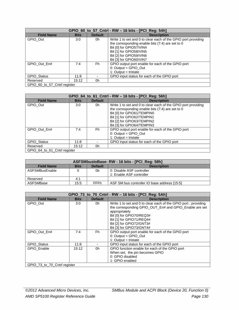
©2012 Advanced Micro Devices, Inc. SMBus Module and ACPI Block (Device 20, Function 0) AMD SP5100 Register Reference Guide Page 130
GPIO_60_to_57_Cntrl - RW – 16 bits - [PCI_Reg: 54h] Field Name Bits Default Description
GPIO_Out 3:0 0h Write 1 to set and 0 to clear each of the GPIO port providing the corresponding enable bits (7:4) are set to 0 Bit [0] for GPIO57/VIN4 Bit [1] for GPIO58/VIN5 Bit [2] for GPIO59/VIN6 Bit [3] for GPIO60/VIN7
GPIO_Out_En# 7:4 Fh GPIO output port enable for each of the GPIO port 0: Output = GPIO_Out 1: Output = tristate
GPIO_Status 11:8 - GPIO input status for each of the GPIO port Reserved 15:12 0h GPIO_60_to_57_Cntrl register
GPIO_64_to_61_Cntrl - RW – 16 bits - [PCI_Reg: 56h] Field Name Bits Default Description
GPIO_Out 3:0 0h Write 1 to set and 0 to clear each of the GPIO port providing the corresponding enable bits (7:4) are set to 0 Bit [0] for GPIO61/TEMPIN0 Bit [1] for GPIO62/TEMPIN1 Bit [2] for GPIO63/TEMPIN2 Bit [3] for GPIO64/TEMPIN3
GPIO_Out_En# 7:4 Fh GPIO output port enable for each of the GPIO port 0: Output = GPIO_Out 1: Output = tristate
GPIO_Status 11:8 - GPIO input status for each of the GPIO port Reserved 15:12 0h GPIO_64_to_61_Cntrl register
ASFSMbusIoBase- RW - 16 bits - [PCI_Reg: 58h] Field Name Bits Default Description
ASFSMBusEnable 0 0b 0: Disable ASF controller 1: Enable ASF controller
Reserved 4:1 ASFSMBase 15:5 FFFh ASF SM bus controller IO base address [15:5]
GPIO_73_to_70_Cntrl - RW – 16 bits - [PCI_Reg: 5Ah] Field Name Bits Default Description
GPIO_Out 3:0 0h Write 1 to set and 0 to clear each of the GPIO port ; providing the corresponding GPIO_OUT_En# and GPIO_Enable are set appropriately Bit [0] for GPIO70/REQ3# Bit [1] for GPIO71/REQ4# Bit [2] for GPIO72/GNT3# Bit [3] for GPIO73/GNT4#
GPIO_Out_En# 7:4 Fh GPIO output port enable for each of the GPIO port 0: Output = GPIO_Out 1: Output = tristate
GPIO_Status 11:8 - GPIO input status for each of the GPIO port GPIO_Enable 15:12 0h GPIO function enable for each of the GPIO port
When set, the pin becomes GPIO 0: GPIO disabled 1: GPIO enabled
GPIO_73_to_70_Cntrl register
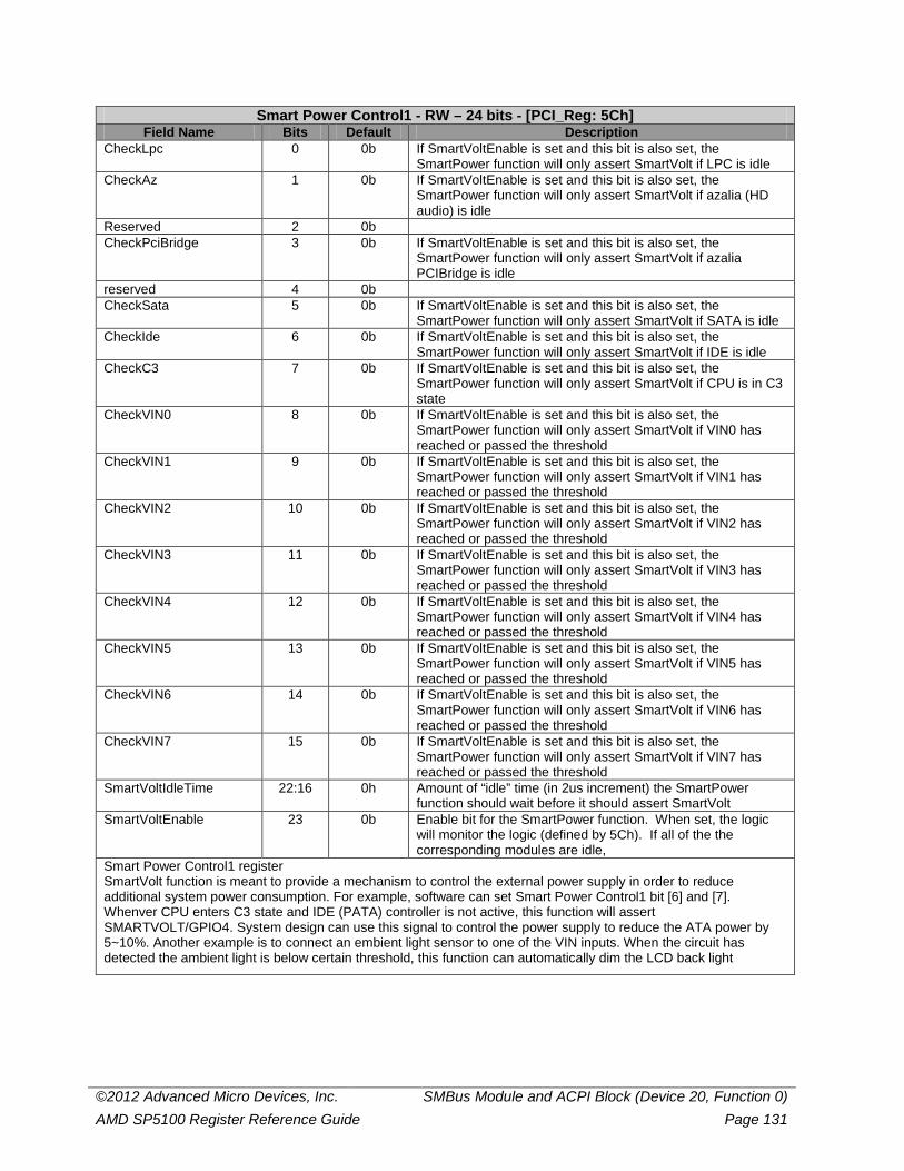
©2012 Advanced Micro Devices, Inc. SMBus Module and ACPI Block (Device 20, Function 0) AMD SP5100 Register Reference Guide Page 131
Smart Power Control1 - RW – 24 bits - [PCI_Reg: 5Ch] Field Name Bits Default Description
CheckLpc 0 0b If SmartVoltEnable is set and this bit is also set, the SmartPower function will only assert SmartVolt if LPC is idle
CheckAz 1 0b If SmartVoltEnable is set and this bit is also set, the SmartPower function will only assert SmartVolt if azalia (HD audio) is idle
Reserved 2 0b CheckPciBridge 3 0b If SmartVoltEnable is set and this bit is also set, the
SmartPower function will only assert SmartVolt if azalia PCIBridge is idle
reserved 4 0b CheckSata 5 0b If SmartVoltEnable is set and this bit is also set, the
SmartPower function will only assert SmartVolt if SATA is idle CheckIde 6 0b If SmartVoltEnable is set and this bit is also set, the
SmartPower function will only assert SmartVolt if IDE is idle CheckC3 7 0b If SmartVoltEnable is set and this bit is also set, the
SmartPower function will only assert SmartVolt if CPU is in C3 state
CheckVIN0 8 0b If SmartVoltEnable is set and this bit is also set, the SmartPower function will only assert SmartVolt if VIN0 has reached or passed the threshold
CheckVIN1 9 0b If SmartVoltEnable is set and this bit is also set, the SmartPower function will only assert SmartVolt if VIN1 has reached or passed the threshold
CheckVIN2 10 0b If SmartVoltEnable is set and this bit is also set, the SmartPower function will only assert SmartVolt if VIN2 has reached or passed the threshold
CheckVIN3 11 0b If SmartVoltEnable is set and this bit is also set, the SmartPower function will only assert SmartVolt if VIN3 has reached or passed the threshold
CheckVIN4 12 0b If SmartVoltEnable is set and this bit is also set, the SmartPower function will only assert SmartVolt if VIN4 has reached or passed the threshold
CheckVIN5 13 0b If SmartVoltEnable is set and this bit is also set, the SmartPower function will only assert SmartVolt if VIN5 has reached or passed the threshold
CheckVIN6 14 0b If SmartVoltEnable is set and this bit is also set, the SmartPower function will only assert SmartVolt if VIN6 has reached or passed the threshold
CheckVIN7 15 0b If SmartVoltEnable is set and this bit is also set, the SmartPower function will only assert SmartVolt if VIN7 has reached or passed the threshold
SmartVoltIdleTime 22:16 0h Amount of “idle” time (in 2us increment) the SmartPower function should wait before it should assert SmartVolt
SmartVoltEnable 23 0b Enable bit for the SmartPower function. When set, the logic will monitor the logic (defined by 5Ch). If all of the the corresponding modules are idle,
Smart Power Control1 register SmartVolt function is meant to provide a mechanism to control the external power supply in order to reduce additional system power consumption. For example, software can set Smart Power Control1 bit [6] and [7]. Whenver CPU enters C3 state and IDE (PATA) controller is not active, this function will assert SMARTVOLT/GPIO4. System design can use this signal to control the power supply to reduce the ATA power by 5~10%. Another example is to connect an embient light sensor to one of the VIN inputs. When the circuit has detected the ambient light is below certain threshold, this function can automatically dim the LCD back light
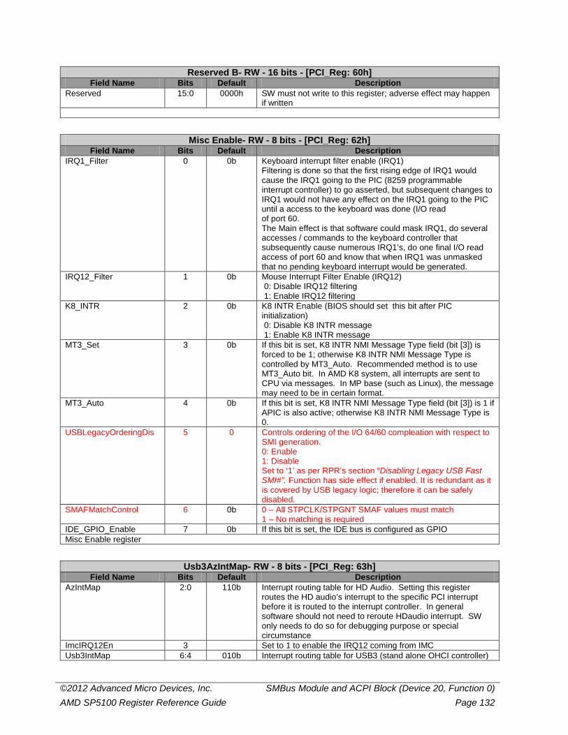
©2012 Advanced Micro Devices, Inc. SMBus Module and ACPI Block (Device 20, Function 0) AMD SP5100 Register Reference Guide Page 132
Reserved B- RW - 16 bits - [PCI_Reg: 60h] Field Name Bits Default Description
Reserved 15:0 0000h SW must not write to this register; adverse effect may happen if written
Misc Enable- RW - 8 bits - [PCI_Reg: 62h] Field Name Bits Default Description
IRQ1_Filter 0 0b Keyboard interrupt filter enable (IRQ1) Filtering is done so that the first rising edge of IRQ1 would cause the IRQ1 going to the PIC (8259 programmable interrupt controller) to go asserted, but subsequent changes to IRQ1 would not have any effect on the IRQ1 going to the PIC until a access to the keyboard was done (I/O read of port 60. The Main effect is that software could mask IRQ1, do several accesses / commands to the keyboard controller that subsequently cause numerous IRQ1’s, do one final I/O read access of port 60 and know that when IRQ1 was unmasked that no pending keyboard interrupt would be generated.
IRQ12_Filter 1 0b Mouse Interrupt Filter Enable (IRQ12) 0: Disable IRQ12 filtering 1: Enable IRQ12 filtering
K8_INTR 2 0b K8 INTR Enable (BIOS should set this bit after PIC initialization) 0: Disable K8 INTR message 1: Enable K8 INTR message
MT3_Set 3 0b If this bit is set, K8 INTR NMI Message Type field (bit [3]) is forced to be 1; otherwise K8 INTR NMI Message Type is controlled by MT3_Auto. Recommended method is to use MT3_Auto bit. In AMD K8 system, all interrupts are sent to CPU via messages. In MP base (such as Linux), the message may need to be in certain format.
MT3_Auto 4 0b If this bit is set, K8 INTR NMI Message Type field (bit [3]) is 1 if APIC is also active; otherwise K8 INTR NMI Message Type is 0.
USBLegacyOrderingDis 5 0 Controls ordering of the I/O 64/60 compleation with respect to SMI generation. 0: Enable 1: Disable Set to ‘1’ as per RPR’s section “Disabling Legacy USB Fast SMI#”. Function has side effect if enabled. It is redundant as it is covered by USB legacy logic; therefore it can be safely disabled.
SMAFMatchControl 6 0b 0 – All STPCLK/STPGNT SMAF values must match 1 – No matching is required
IDE_GPIO_Enable 7 0b If this bit is set, the IDE bus is configured as GPIO Misc Enable register
Usb3AzIntMap- RW - 8 bits - [PCI_Reg: 63h] Field Name Bits Default Description
AzIntMap 2:0 110b Interrupt routing table for HD Audio. Setting this register routes the HD audio’s interrupt to the specific PCI interrupt before it is routed to the interrupt controller. In general software should not need to reroute HDaudio interrupt. SW only needs to do so for debugging purpose or special circumstance
ImcIRQ12En 3 Set to 1 to enable the IRQ12 coming from IMC Usb3IntMap 6:4 010b Interrupt routing table for USB3 (stand alone OHCI controller)
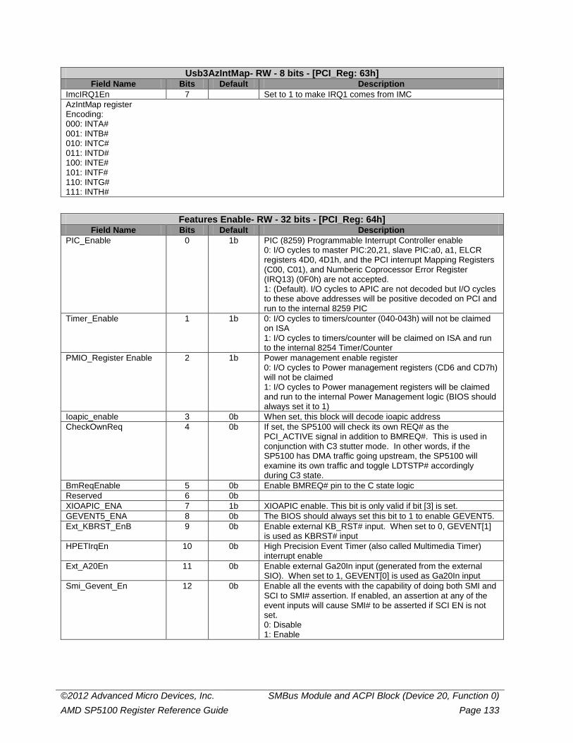
©2012 Advanced Micro Devices, Inc. SMBus Module and ACPI Block (Device 20, Function 0) AMD SP5100 Register Reference Guide Page 133
Usb3AzIntMap- RW - 8 bits - [PCI_Reg: 63h] Field Name Bits Default Description
ImcIRQ1En 7 Set to 1 to make IRQ1 comes from IMC AzIntMap register Encoding: 000: INTA# 001: INTB# 010: INTC# 011: INTD# 100: INTE# 101: INTF# 110: INTG# 111: INTH#
Features Enable- RW - 32 bits - [PCI_Reg: 64h] Field Name Bits Default Description
PIC_Enable
0 1b PIC (8259) Programmable Interrupt Controller enable 0: I/O cycles to master PIC:20,21, slave PIC:a0, a1, ELCR registers 4D0, 4D1h, and the PCI interrupt Mapping Registers (C00, C01), and Numberic Coprocessor Error Register (IRQ13) (0F0h) are not accepted. 1: (Default). I/O cycles to APIC are not decoded but I/O cycles to these above addresses will be positive decoded on PCI and run to the internal 8259 PIC
Timer_Enable 1 1b 0: I/O cycles to timers/counter (040-043h) will not be claimed on ISA 1: I/O cycles to timers/counter will be claimed on ISA and run to the internal 8254 Timer/Counter
PMIO_Register Enable
2 1b Power management enable register 0: I/O cycles to Power management registers (CD6 and CD7h) will not be claimed 1: I/O cycles to Power management registers will be claimed and run to the internal Power Management logic (BIOS should always set it to 1)
Ioapic_enable 3 0b When set, this block will decode ioapic address CheckOwnReq
4 0b If set, the SP5100 will check its own REQ# as the PCI_ACTIVE signal in addition to BMREQ#. This is used in conjunction with C3 stutter mode. In other words, if the SP5100 has DMA traffic going upstream, the SP5100 will examine its own traffic and toggle LDTSTP# accordingly during C3 state.
BmReqEnable 5 0b Enable BMREQ# pin to the C state logic Reserved 6 0b XIOAPIC_ENA 7 1b XIOAPIC enable. This bit is only valid if bit [3] is set. GEVENT5_ENA 8 0b The BIOS should always set this bit to 1 to enable GEVENT5. Ext_KBRST_EnB 9 0b Enable external KB_RST# input. When set to 0, GEVENT[1]
is used as KBRST# input HPETIrqEn 10 0b High Precision Event Timer (also called Multimedia Timer)
interrupt enable Ext_A20En
11 0b Enable external Ga20In input (generated from the external SIO). When set to 1, GEVENT[0] is used as Ga20In input
Smi_Gevent_En 12 0b Enable all the events with the capability of doing both SMI and SCI to SMI# assertion. If enabled, an assertion at any of the event inputs will cause SMI# to be asserted if SCI EN is not set. 0: Disable 1: Enable
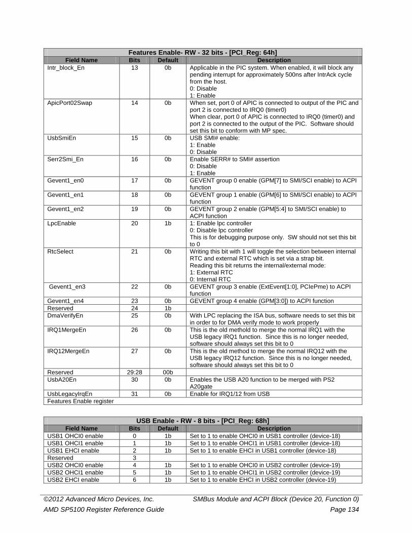
©2012 Advanced Micro Devices, Inc. SMBus Module and ACPI Block (Device 20, Function 0) AMD SP5100 Register Reference Guide Page 134
Features Enable- RW - 32 bits - [PCI_Reg: 64h] Field Name Bits Default Description
Intr_block_En
13 0b Applicable in the PIC system. When enabled, it will block any pending interrupt for approximately 500ns after IntrAck cycle from the host. 0: Disable 1: Enable
ApicPort02Swap
14 0b When set, port 0 of APIC is connected to output of the PIC and port 2 is connected to IRQ0 (timer0) When clear, port 0 of APIC is connected to IRQ0 (timer0) and port 2 is connected to the output of the PIC. Software should set this bit to conform with MP spec.
UsbSmiEn
15 0b USB SMI# enable: 1: Enable 0: Disable
Serr2Smi_En 16 0b Enable SERR# to SMI# assertion 0: Disable 1: Enable
Gevent1_en0 17 0b GEVENT group 0 enable (GPM[7] to SMI/SCI enable) to ACPI function
Gevent1_en1 18 0b GEVENT group 1 enable (GPM[6] to SMI/SCI enable) to ACPI function
Gevent1_en2 19 0b GEVENT group 2 enable (GPM[5:4] to SMI/SCI enable) to ACPI function
LpcEnable 20 1b 1: Enable lpc controller 0: Disable lpc controller This is for debugging purpose only. SW should not set this bit to 0
RtcSelect 21 0b Writing this bit with 1 will toggle the selection between internal RTC and external RTC which is set via a strap bit. Reading this bit returns the internal/external mode: 1: External RTC 0: Internal RTC
Gevent1_en3 22 0b GEVENT group 3 enable (ExtEvent[1:0], PCIePme) to ACPI function
Gevent1_en4 23 0b GEVENT group 4 enable (GPM[3:0]) to ACPI function Reserved 24 1b DmaVerifyEn 25 0b With LPC replacing the ISA bus, software needs to set this bit
in order to for DMA verify mode to work properly IRQ1MergeEn 26 0b This is the old methold to merge the normal IRQ1 with the
USB legacy IRQ1 function. Since this is no longer needed, software should always set this bit to 0
IRQ12MergeEn 27 0b This is the old method to merge the normal IRQ12 with the USB legacy IRQ12 function. Since this is no longer needed, software should always set this bit to 0
Reserved 29:28 00b UsbA20En 30 0b Enables the USB A20 function to be merged with PS2
A20gate UsbLegacyIrqEn 31 0b Enable for IRQ1/12 from USB Features Enable register
USB Enable - RW - 8 bits - [PCI_Reg: 68h] Field Name Bits Default Description
USB1 OHCI0 enable 0 1b Set to 1 to enable OHCI0 in USB1 controller (device-18) USB1 OHCI1 enable 1 1b Set to 1 to enable OHCI1 in USB1 controller (device-18) USB1 EHCI enable 2 1b Set to 1 to enable EHCI in USB1 controller (device-18) Reserved 3 USB2 OHCI0 enable 4 1b Set to 1 to enable OHCI0 in USB2 controller (device-19) USB2 OHCI1 enable 5 1b Set to 1 to enable OHCI1 in USB2 controller (device-19) USB2 EHCI enable 6 1b Set to 1 to enable EHCI in USB2 controller (device-19)
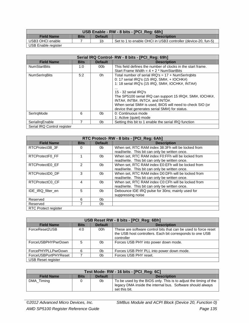
©2012 Advanced Micro Devices, Inc. SMBus Module and ACPI Block (Device 20, Function 0) AMD SP5100 Register Reference Guide Page 135
USB Enable - RW - 8 bits - [PCI_Reg: 68h] Field Name Bits Default Description
USB3 OHCI enable 7 1b Set to 1 to enable OHCI in USB3 controller (device-20, fun-5) USB Enable register
Serial lRQ Control- RW - 8 bits - [PCI_Reg: 69h] Field Name Bits Default Description
NumStartBits 1:0 00b This field defines the number of clocks in the start frame. Start Frame Width = 4 + 2 * NumStartBits
NumSerIrqBits 5:2 0h Total number of serial IRQ's = 17 + NumSerIrqbits 0: 17 serial IRQ's (15 IRQ, SMI#, + IOCHK#) 1: 18 serial IRQ's (15 IRQ, SMI#, IOCHK#, INTA#) ... 15 - 32 serial IRQ's The SP5100 serial IRQ can support 15 IRQ#, SMI#, IOCHK#, INTA#, INTB#, INTC#, and INTD#. When serial SMI# is used, BIOS will need to check SIO (or device that generates serial SMI#) for status.
SerIrqMode 6 0b 0: Continuous mode 1: Active (quiet) mode
SerialIrqEnable 7 0b Setting this bit to 1 enable the serial IRQ function Serial lRQ Control register
RTC Protect- RW - 8 bits - [PCI_Reg: 6Ah] Field Name Bits Default Description
RTCProtect38_3F 0 0b When set, RTC RAM index 38:3Fh will be locked from read/write. This bit can only be written once.
RTCProtectF0_FF 1 0b When set, RTC RAM index F0:FFh will be locked from read/write. This bit can only be written once.
RTCProtectE0_EF 2 0b When set, RTC RAM index E0:EFh will be locked from read/write. This bit can only be written once.
RTCProtectD0_DF 3 0b When set, RTC RAM index D0:DFh will be locked from read/write. This bit can only be written once.
RTCProtectC0_CF 4 0b When set, RTC RAM index C0:CFh will be locked from read/write. This bit can only be written once.
IDE_IRQ_filter_en 5 0b Debounce IDE IRQ pulse for 30ns; mainly used for suppressing noise
Reserved 6 0b Reserved 7 0b RTC Protect register
USB Reset RW - 8 bits - [PCI_Reg: 6Bh] Field Name Bits Default Description
ForceReset2USB 4:0 00h These are software control bits that can be used to force reset the USB host controllers. Each bit corresponds to one USB controller
ForceUSBPHYPwrDown
5 0b Forces USB PHY into power down mode.
ForcePHYPLLPwrDown 6 0b Forces USB PHY PLL into power down mode. ForceUSBPortPHYReset 7 0b Forces USB PHY reset. USB Reset register
Test Mode- RW - 16 bits - [PCI_Reg: 6C] Field Name Bits Default Description
DMA_Timing
0 0b To be used by the BIOS only. This is to adjust the timing of the legacy DMA inside the internal bus. Software should always set this bit.
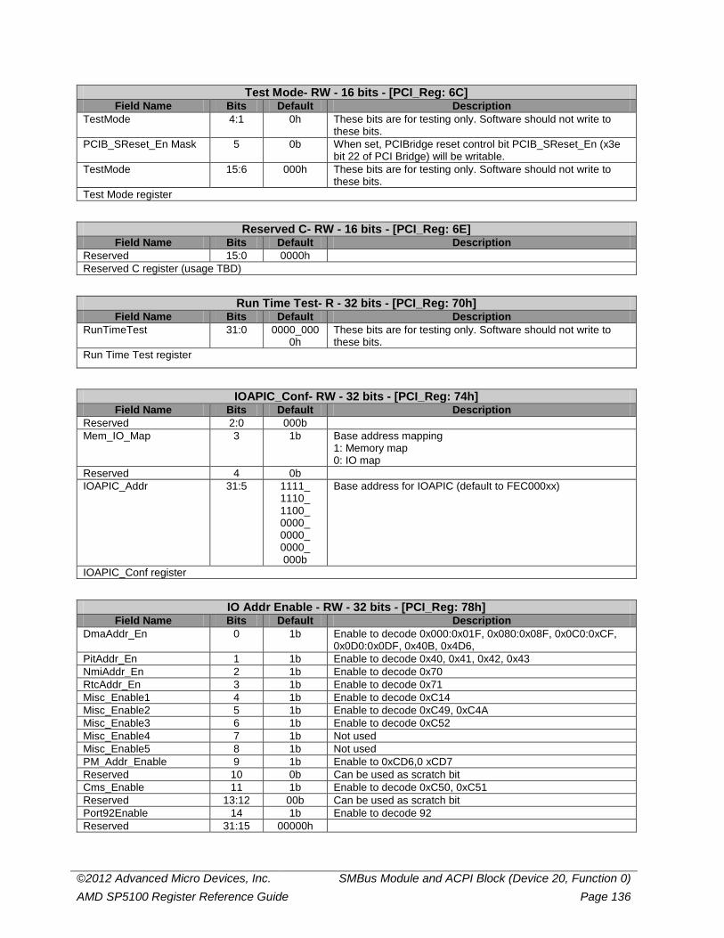
©2012 Advanced Micro Devices, Inc. SMBus Module and ACPI Block (Device 20, Function 0) AMD SP5100 Register Reference Guide Page 136
Test Mode- RW - 16 bits - [PCI_Reg: 6C] Field Name Bits Default Description
TestMode
4:1 0h These bits are for testing only. Software should not write to these bits.
PCIB_SReset_En Mask 5 0b When set, PCIBridge reset control bit PCIB_SReset_En (x3e bit 22 of PCI Bridge) will be writable.
TestMode
15:6 000h These bits are for testing only. Software should not write to these bits.
Test Mode register
Reserved C- RW - 16 bits - [PCI_Reg: 6E] Field Name Bits Default Description
Reserved 15:0 0000h Reserved C register (usage TBD)
Run Time Test- R - 32 bits - [PCI_Reg: 70h] Field Name Bits Default Description
RunTimeTest
31:0 0000_0000h
These bits are for testing only. Software should not write to these bits.
Run Time Test register
IOAPIC_Conf- RW - 32 bits - [PCI_Reg: 74h] Field Name Bits Default Description
Reserved 2:0 000b Mem_IO_Map 3 1b Base address mapping
1: Memory map 0: IO map
Reserved 4 0b IOAPIC_Addr 31:5 1111_
1110_ 1100_ 0000_ 0000_ 0000_ 000b
Base address for IOAPIC (default to FEC000xx)
IOAPIC_Conf register
IO Addr Enable - RW - 32 bits - [PCI_Reg: 78h] Field Name Bits Default Description
DmaAddr_En 0 1b Enable to decode 0x000:0x01F, 0x080:0x08F, 0x0C0:0xCF, 0x0D0:0x0DF, 0x40B, 0x4D6,
PitAddr_En 1 1b Enable to decode 0x40, 0x41, 0x42, 0x43 NmiAddr_En 2 1b Enable to decode 0x70 RtcAddr_En 3 1b Enable to decode 0x71 Misc_Enable1 4 1b Enable to decode 0xC14 Misc_Enable2 5 1b Enable to decode 0xC49, 0xC4A Misc_Enable3 6 1b Enable to decode 0xC52 Misc_Enable4 7 1b Not used Misc_Enable5 8 1b Not used PM_Addr_Enable 9 1b Enable to 0xCD6,0 xCD7 Reserved 10 0b Can be used as scratch bit Cms_Enable 11 1b Enable to decode 0xC50, 0xC51 Reserved 13:12 00b Can be used as scratch bit Port92Enable 14 1b Enable to decode 92 Reserved 31:15 00000h
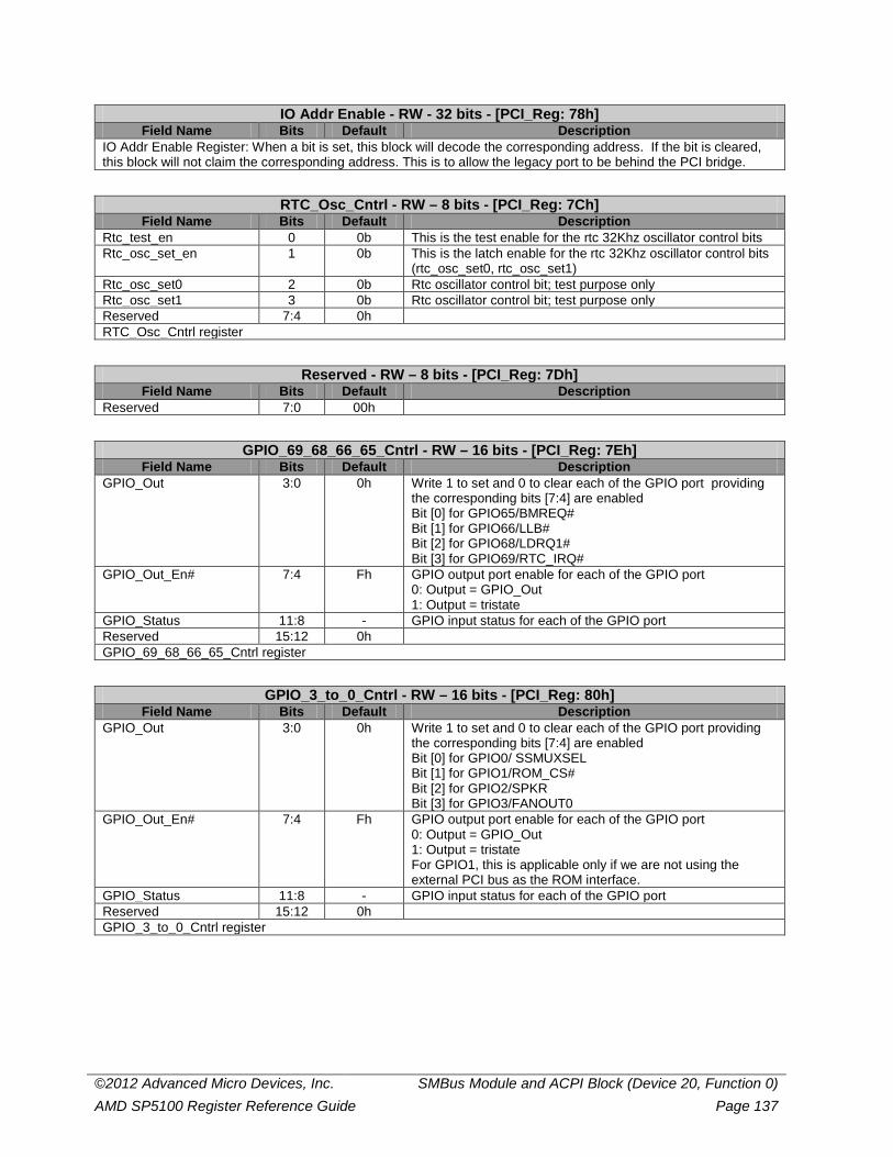
©2012 Advanced Micro Devices, Inc. SMBus Module and ACPI Block (Device 20, Function 0) AMD SP5100 Register Reference Guide Page 137
IO Addr Enable - RW - 32 bits - [PCI_Reg: 78h] Field Name Bits Default Description
IO Addr Enable Register: When a bit is set, this block will decode the corresponding address. If the bit is cleared, this block will not claim the corresponding address. This is to allow the legacy port to be behind the PCI bridge.
RTC_Osc_Cntrl - RW – 8 bits - [PCI_Reg: 7Ch] Field Name Bits Default Description
Rtc_test_en 0 0b This is the test enable for the rtc 32Khz oscillator control bits Rtc_osc_set_en 1 0b This is the latch enable for the rtc 32Khz oscillator control bits
(rtc_osc_set0, rtc_osc_set1) Rtc_osc_set0 2 0b Rtc oscillator control bit; test purpose only Rtc_osc_set1 3 0b Rtc oscillator control bit; test purpose only Reserved 7:4 0h RTC_Osc_Cntrl register
Reserved - RW – 8 bits - [PCI_Reg: 7Dh] Field Name Bits Default Description
Reserved 7:0 00h
GPIO_69_68_66_65_Cntrl - RW – 16 bits - [PCI_Reg: 7Eh] Field Name Bits Default Description
GPIO_Out 3:0 0h Write 1 to set and 0 to clear each of the GPIO port providing the corresponding bits [7:4] are enabled Bit [0] for GPIO65/BMREQ# Bit [1] for GPIO66/LLB# Bit [2] for GPIO68/LDRQ1# Bit [3] for GPIO69/RTC_IRQ#
GPIO_Out_En# 7:4 Fh GPIO output port enable for each of the GPIO port 0: Output = GPIO_Out 1: Output = tristate
GPIO_Status 11:8 - GPIO input status for each of the GPIO port Reserved 15:12 0h GPIO_69_68_66_65_Cntrl register
GPIO_3_to_0_Cntrl - RW – 16 bits - [PCI_Reg: 80h] Field Name Bits Default Description
GPIO_Out 3:0 0h Write 1 to set and 0 to clear each of the GPIO port providing the corresponding bits [7:4] are enabled Bit [0] for GPIO0/ SSMUXSEL Bit [1] for GPIO1/ROM_CS# Bit [2] for GPIO2/SPKR Bit [3] for GPIO3/FANOUT0
GPIO_Out_En# 7:4 Fh GPIO output port enable for each of the GPIO port 0: Output = GPIO_Out 1: Output = tristate For GPIO1, this is applicable only if we are not using the external PCI bus as the ROM interface.
GPIO_Status 11:8 - GPIO input status for each of the GPIO port Reserved 15:12 0h GPIO_3_to_0_Cntrl register
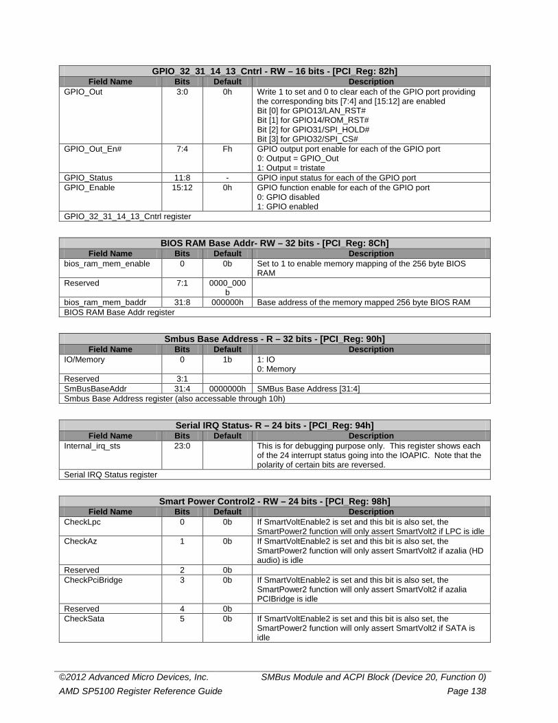
©2012 Advanced Micro Devices, Inc. SMBus Module and ACPI Block (Device 20, Function 0) AMD SP5100 Register Reference Guide Page 138
GPIO_32_31_14_13_Cntrl - RW – 16 bits - [PCI_Reg: 82h] Field Name Bits Default Description
GPIO_Out 3:0 0h Write 1 to set and 0 to clear each of the GPIO port providing the corresponding bits [7:4] and [15:12] are enabled Bit [0] for GPIO13/LAN_RST# Bit [1] for GPIO14/ROM_RST# Bit [2] for GPIO31/SPI_HOLD# Bit [3] for GPIO32/SPI_CS#
GPIO_Out_En# 7:4 Fh GPIO output port enable for each of the GPIO port 0: Output = GPIO_Out 1: Output = tristate
GPIO_Status 11:8 - GPIO input status for each of the GPIO port GPIO_Enable 15:12 0h GPIO function enable for each of the GPIO port
0: GPIO disabled 1: GPIO enabled
GPIO_32_31_14_13_Cntrl register
BIOS RAM Base Addr- RW – 32 bits - [PCI_Reg: 8Ch] Field Name Bits Default Description
bios_ram_mem_enable 0 0b Set to 1 to enable memory mapping of the 256 byte BIOS RAM
Reserved 7:1 0000_000b
bios_ram_mem_baddr 31:8 000000h Base address of the memory mapped 256 byte BIOS RAM BIOS RAM Base Addr register
Smbus Base Address - R – 32 bits - [PCI_Reg: 90h] Field Name Bits Default Description
IO/Memory 0 1b 1: IO 0: Memory
Reserved 3:1 SmBusBaseAddr 31:4 0000000h SMBus Base Address [31:4] Smbus Base Address register (also accessable through 10h)
Serial IRQ Status- R – 24 bits - [PCI_Reg: 94h] Field Name Bits Default Description
Internal_irq_sts 23:0 This is for debugging purpose only. This register shows each of the 24 interrupt status going into the IOAPIC. Note that the polarity of certain bits are reversed.
Serial IRQ Status register
Smart Power Control2 - RW – 24 bits - [PCI_Reg: 98h] Field Name Bits Default Description
CheckLpc 0 0b If SmartVoltEnable2 is set and this bit is also set, the SmartPower2 function will only assert SmartVolt2 if LPC is idle
CheckAz 1 0b If SmartVoltEnable2 is set and this bit is also set, the SmartPower2 function will only assert SmartVolt2 if azalia (HD audio) is idle
Reserved 2 0b CheckPciBridge 3 0b If SmartVoltEnable2 is set and this bit is also set, the
SmartPower2 function will only assert SmartVolt2 if azalia PCIBridge is idle
Reserved 4 0b CheckSata 5 0b If SmartVoltEnable2 is set and this bit is also set, the
SmartPower2 function will only assert SmartVolt2 if SATA is idle
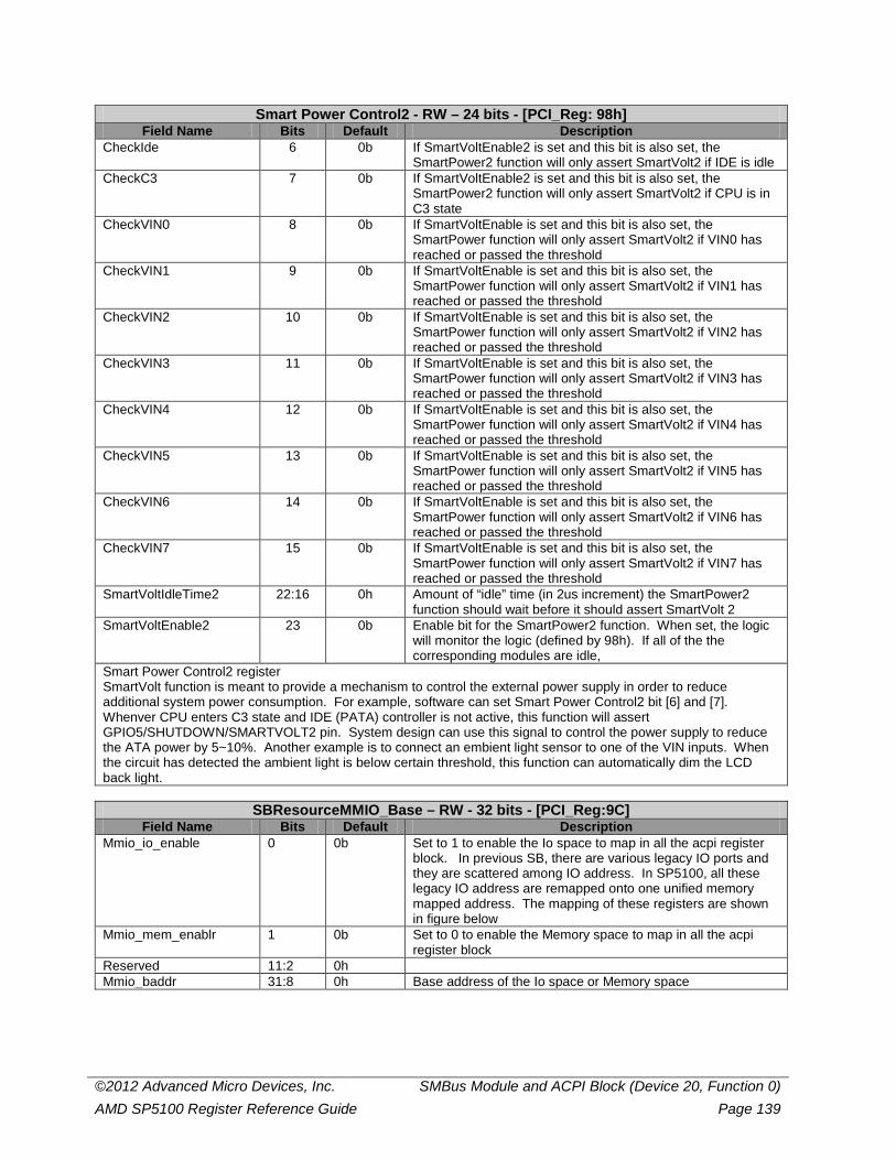
©2012 Advanced Micro Devices, Inc. SMBus Module and ACPI Block (Device 20, Function 0) AMD SP5100 Register Reference Guide Page 139
Smart Power Control2 - RW – 24 bits - [PCI_Reg: 98h] Field Name Bits Default Description
CheckIde 6 0b If SmartVoltEnable2 is set and this bit is also set, the SmartPower2 function will only assert SmartVolt2 if IDE is idle
CheckC3 7 0b If SmartVoltEnable2 is set and this bit is also set, the SmartPower2 function will only assert SmartVolt2 if CPU is in C3 state
CheckVIN0 8 0b If SmartVoltEnable is set and this bit is also set, the SmartPower function will only assert SmartVolt2 if VIN0 has reached or passed the threshold
CheckVIN1 9 0b If SmartVoltEnable is set and this bit is also set, the SmartPower function will only assert SmartVolt2 if VIN1 has reached or passed the threshold
CheckVIN2 10 0b If SmartVoltEnable is set and this bit is also set, the SmartPower function will only assert SmartVolt2 if VIN2 has reached or passed the threshold
CheckVIN3 11 0b If SmartVoltEnable is set and this bit is also set, the SmartPower function will only assert SmartVolt2 if VIN3 has reached or passed the threshold
CheckVIN4 12 0b If SmartVoltEnable is set and this bit is also set, the SmartPower function will only assert SmartVolt2 if VIN4 has reached or passed the threshold
CheckVIN5 13 0b If SmartVoltEnable is set and this bit is also set, the SmartPower function will only assert SmartVolt2 if VIN5 has reached or passed the threshold
CheckVIN6 14 0b If SmartVoltEnable is set and this bit is also set, the SmartPower function will only assert SmartVolt2 if VIN6 has reached or passed the threshold
CheckVIN7 15 0b If SmartVoltEnable is set and this bit is also set, the SmartPower function will only assert SmartVolt2 if VIN7 has reached or passed the threshold
SmartVoltIdleTime2 22:16 0h Amount of “idle” time (in 2us increment) the SmartPower2 function should wait before it should assert SmartVolt 2
SmartVoltEnable2 23 0b Enable bit for the SmartPower2 function. When set, the logic will monitor the logic (defined by 98h). If all of the the corresponding modules are idle,
Smart Power Control2 register SmartVolt function is meant to provide a mechanism to control the external power supply in order to reduce additional system power consumption. For example, software can set Smart Power Control2 bit [6] and [7]. Whenver CPU enters C3 state and IDE (PATA) controller is not active, this function will assert GPIO5/SHUTDOWN/SMARTVOLT2 pin. System design can use this signal to control the power supply to reduce the ATA power by 5~10%. Another example is to connect an embient light sensor to one of the VIN inputs. When the circuit has detected the ambient light is below certain threshold, this function can automatically dim the LCD back light.
SBResourceMMIO_Base – RW - 32 bits - [PCI_Reg:9C]
Field Name Bits Default Description Mmio_io_enable 0 0b Set to 1 to enable the Io space to map in all the acpi register
block. In previous SB, there are various legacy IO ports and they are scattered among IO address. In SP5100, all these legacy IO address are remapped onto one unified memory mapped address. The mapping of these registers are shown in figure below
Mmio_mem_enablr 1 0b Set to 0 to enable the Memory space to map in all the acpi register block
Reserved 11:2 0h Mmio_baddr 31:8 0h Base address of the Io space or Memory space
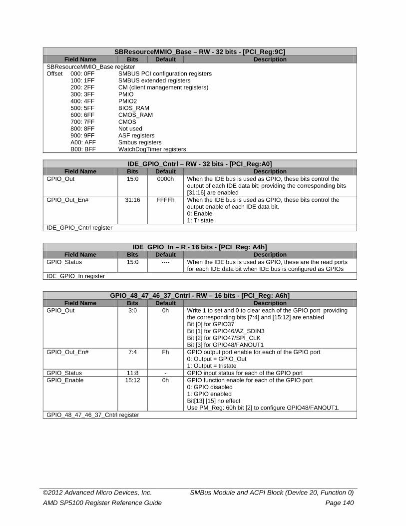
©2012 Advanced Micro Devices, Inc. SMBus Module and ACPI Block (Device 20, Function 0) AMD SP5100 Register Reference Guide Page 140
SBResourceMMIO_Base – RW - 32 bits - [PCI_Reg:9C] Field Name Bits Default Description
SBResourceMMIO_Base register Offset 000: 0FF SMBUS PCI configuration registers 100: 1FF SMBUS extended registers 200: 2FF CM (client management registers) 300: 3FF PMIO 400: 4FF PMIO2 500: 5FF BIOS_RAM 600: 6FF CMOS_RAM 700: 7FF CMOS 800: 8FF Not used 900: 9FF ASF registers A00: AFF Smbus registers B00: BFF WatchDogTimer registers
IDE_GPIO_Cntrl – RW - 32 bits - [PCI_Reg:A0]
Field Name Bits Default Description GPIO_Out 15:0 0000h When the IDE bus is used as GPIO, these bits control the
output of each IDE data bit; providing the corresponding bits [31:16] are enabled
GPIO_Out_En# 31:16 FFFFh When the IDE bus is used as GPIO, these bits control the output enable of each IDE data bit. 0: Enable 1: Tristate
IDE_GPIO_Cntrl register
IDE_GPIO_In – R - 16 bits - [PCI_Reg: A4h] Field Name Bits Default Description
GPIO_Status 15:0 ---- When the IDE bus is used as GPIO, these are the read ports for each IDE data bit when IDE bus is configured as GPIOs
IDE_GPIO_In register
GPIO_48_47_46_37_Cntrl - RW – 16 bits - [PCI_Reg: A6h] Field Name Bits Default Description
GPIO_Out 3:0 0h Write 1 to set and 0 to clear each of the GPIO port providing the corresponding bits [7:4] and [15:12] are enabled Bit [0] for GPIO37 Bit [1] for GPIO46/AZ_SDIN3 Bit [2] for GPIO47/SPI_CLK Bit [3] for GPIO48/FANOUT1
GPIO_Out_En# 7:4 Fh GPIO output port enable for each of the GPIO port 0: Output = GPIO_Out 1: Output = tristate
GPIO_Status 11:8 - GPIO input status for each of the GPIO port GPIO_Enable 15:12 0h GPIO function enable for each of the GPIO port
0: GPIO disabled 1: GPIO enabled Bit[13] [15] no effect Use PM_Reg: 60h bit [2] to configure GPIO48/FANOUT1.
GPIO_48_47_46_37_Cntrl register
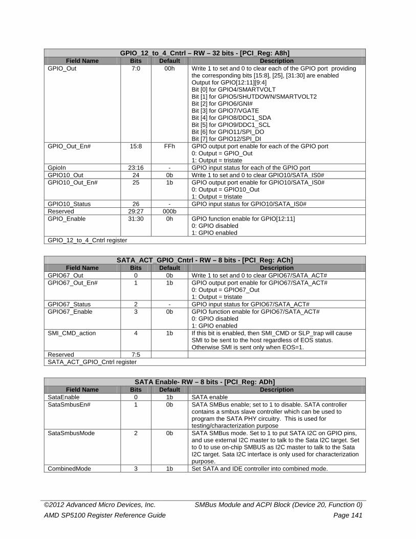
©2012 Advanced Micro Devices, Inc. SMBus Module and ACPI Block (Device 20, Function 0) AMD SP5100 Register Reference Guide Page 141
GPIO_12_to_4_Cntrl – RW – 32 bits - [PCI_Reg: A8h] Field Name Bits Default Description
GPIO_Out 7:0 00h Write 1 to set and 0 to clear each of the GPIO port providing the corresponding bits [15:8], [25], [31:30] are enabled Output for GPIO[12:11][9:4] Bit [0] for GPIO4/SMARTVOLT Bit [1] for GPIO5/SHUTDOWN/SMARTVOLT2 Bit [2] for GPIO6/GNI# Bit [3] for GPIO7/VGATE Bit [4] for GPIO8/DDC1_SDA Bit [5] for GPIO9/DDC1_SCL Bit [6] for GPIO11/SPI_DO Bit [7] for GPIO12/SPI_DI
GPIO_Out_En# 15:8 FFh GPIO output port enable for each of the GPIO port 0: Output = GPIO_Out 1: Output = tristate
GpioIn 23:16 - GPIO input status for each of the GPIO port GPIO10_Out 24 0b Write 1 to set and 0 to clear GPIO10/SATA_IS0# GPIO10_Out_En# 25 1b GPIO output port enable for GPIO10/SATA_IS0#
0: Output = GPIO10_Out 1: Output = tristate
GPIO10_Status 26 - GPIO input status for GPIO10/SATA_IS0# Reserved 29:27 000b GPIO_Enable 31:30 0h GPIO function enable for GPIO[12:11]
0: GPIO disabled 1: GPIO enabled
GPIO_12_to_4_Cntrl register
SATA_ACT_GPIO_Cntrl - RW – 8 bits - [PCI_Reg: ACh] Field Name Bits Default Description
GPIO67_Out 0 0b Write 1 to set and 0 to clear GPIO67/SATA_ACT# GPIO67_Out_En# 1 1b GPIO output port enable for GPIO67/SATA_ACT#
0: Output = GPIO67_Out 1: Output = tristate
GPIO67_Status 2 - GPIO input status for GPIO67/SATA_ACT# GPIO67_Enable 3 0b GPIO function enable for GPIO67/SATA_ACT#
0: GPIO disabled 1: GPIO enabled
SMI_CMD_action
4 1b If this bit is enabled, then SMI_CMD or SLP_trap will cause SMI to be sent to the host regardless of EOS status. Otherwise SMI is sent only when EOS=1.
Reserved 7:5 SATA_ACT_GPIO_Cntrl register
SATA Enable- RW – 8 bits - [PCI_Reg: ADh] Field Name Bits Default Description
SataEnable 0 1b SATA enable SataSmbusEn# 1 0b SATA SMBus enable; set to 1 to disable. SATA controller
contains a smbus slave controller which can be used to program the SATA PHY circuitry. This is used for testing/characterization purpose
SataSmbusMode 2 0b SATA SMBus mode. Set to 1 to put SATA I2C on GPIO pins, and use external I2C master to talk to the Sata I2C target. Set to 0 to use on-chip SMBUS as I2C master to talk to the Sata I2C target. Sata I2C interface is only used for characterization purpose.
CombinedMode 3 1b Set SATA and IDE controller into combined mode.
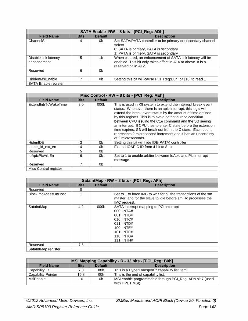
©2012 Advanced Micro Devices, Inc. SMBus Module and ACPI Block (Device 20, Function 0) AMD SP5100 Register Reference Guide Page 142
SATA Enable- RW – 8 bits - [PCI_Reg: ADh] Field Name Bits Default Description
ChannelSel 4 0b Set SATA/PATA controller to be primary or secondary channel select 0: SATA is primary, PATA is secondary 1: PATA is primery, SATA is secondary
Disable link latency enhancement
5 1b When cleared, an enhancement of SATA link latency will be enabled. This bit only takes effect in A14 or above. It is a reserved bit in A12.
Reserved
6 0b
HiddenMsiEnable 7 0b Setting this bit will cause PCI_Reg:B0h, bit [16] to read 1 SATA Enable register
Misc Control - RW – 8 bits - [PCI_Reg: AEh] Field Name Bits Default Description
ExtendIntrToWakeTime
2:0 000b This is used in K8 system to extend the interrupt break event status. Whenever there is an apic interrupt, this logic will extend the break event status by the amount of time defined by this register. This is to avoid potential race condition between CPU issuing the C1e command and the SB seeing an interrupt. If CPU tries to enter C state before the extension time expires, SB will break out from the C state. Each count represents 2 microsecond increment and it has an uncertainty of 2 microseconds.
HidenIDE 3 0b Setting this bit will hide IDE(PATA) controller. Ioapic_id_ext_en 4 0b Extend IOAPIC ID from 4-bit to 8-bit. Reserved 5 0b IoApicPicArbEn 6 0b Set to 1 to enable arbiter between IoApic and Pic interrupt
message. Reserved 7 0b Misc Control register
SataIntMap - RW – 8 bits - [PCI_Reg: AFh] Field Name Bits Default Description
Reserved 0 BlockImcAcessOnHost 1 Set to 1 to force IMC to wait for all the transactions of the sm
master, and for the slave to idle before sm Hc processes the IMC request.
SataIntMap 4:2 000b SATA interrupt mapping to PCI interrupt 000: INTA# 001: INTB# 010: INTC# 011: INTD# 100: INTE# 101: INTF# 110: INTG# 111: INTH#
Reserved 7:5 SataIntMap register
MSI Mapping Capability - R - 32 bits - [PCI_Reg: B0h] Field Name Bits Default Description
Capability ID 7:0 08h This is a HyperTransportTM capability list item. Capability Pointer 15:8 00h This is the end of capability list. MsiEnable 16 0b MSI enable programmable through PCI_Reg: ADh bit 7 (used
with HPET MSI)
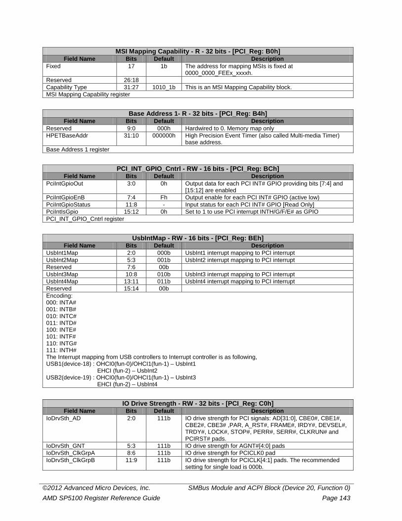
©2012 Advanced Micro Devices, Inc. SMBus Module and ACPI Block (Device 20, Function 0) AMD SP5100 Register Reference Guide Page 143
MSI Mapping Capability - R - 32 bits - [PCI_Reg: B0h] Field Name Bits Default Description
Fixed 17 1b The address for mapping MSIs is fixed at 0000_0000_FEEx_xxxxh.
Reserved 26:18 Capability Type 31:27 1010_1b This is an MSI Mapping Capability block. MSI Mapping Capability register
Base Address 1- R - 32 bits - [PCI_Reg: B4h] Field Name Bits Default Description
Reserved 9:0 000h Hardwired to 0. Memory map only HPETBaseAddr 31:10 000000h High Precision Event Timer (also called Multi-media Timer)
base address. Base Address 1 register
PCI_INT_GPIO_Cntrl - RW - 16 bits - [PCI_Reg: BCh] Field Name Bits Default Description
PciIntGpioOut 3:0 0h Output data for each PCI INT# GPIO providing bits [7:4] and [15:12] are enabled
PciIntGpioEnB 7:4 Fh Output enable for each PCI INT# GPIO (active low) PciIntGpioStatus 11:8 - Input status for each PCI INT# GPIO [Read Only] PciIntIsGpio 15:12 0h Set to 1 to use PCI interrupt INTH/G/F/E# as GPIO PCI_INT_GPIO_Cntrl register
UsbIntMap - RW - 16 bits - [PCI_Reg: BEh] Field Name Bits Default Description
UsbInt1Map 2:0 000b UsbInt1 interrupt mapping to PCI interrupt UsbInt2Map 5:3 001b UsbInt2 interrupt mapping to PCI interrupt Reserved 7:6 00b UsbInt3Map 10:8 010b UsbInt3 interrupt mapping to PCI interrupt UsbInt4Map 13:11 011b UsbInt4 interrupt mapping to PCI interrupt Reserved 15:14 00b Encoding: 000: INTA# 001: INTB# 010: INTC# 011: INTD# 100: INTE# 101: INTF# 110: INTG# 111: INTH# The Interrupt mapping from USB controllers to Interrupt controller is as following, USB1(device-18) : OHCI0(fun-0)/OHCI1(fun-1) – UsbInt1 EHCI (fun-2) – UsbInt2 USB2(device-19) : OHCI0(fun-0)/OHCI1(fun-1) – UsbInt3 EHCI (fun-2) – UsbInt4
IO Drive Strength - RW - 32 bits - [PCI_Reg: C0h] Field Name Bits Default Description
IoDrvSth_AD 2:0 111b IO drive strength for PCI signals: AD[31:0], CBE0#, CBE1#, CBE2#, CBE3# ,PAR, A_RST#, FRAME#, IRDY#, DEVSEL#, TRDY#, LOCK#, STOP#, PERR#, SERR#, CLKRUN# and PCIRST# pads.
IoDrvSth_GNT 5:3 111b IO drive strength for AGNT#[4:0] pads IoDrvSth_ClkGrpA 8:6 111b IO drive strength for PCICLK0 pad IoDrvSth_ClkGrpB 11:9 111b IO drive strength for PCICLK[4:1] pads. The recommended
setting for single load is 000b.
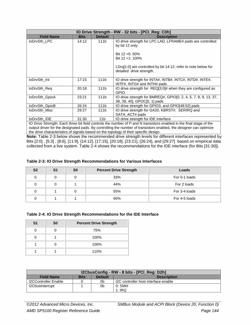
©2012 Advanced Micro Devices, Inc. SMBus Module and ACPI Block (Device 20, Function 0) AMD SP5100 Register Reference Guide Page 144
IO Drive Strength - RW - 32 bits - [PCI_Reg: C0h] Field Name Bits Default Description
IoDrvSth_LPC 14:12 111b IO drive strength for LPC LAD, LFRAME# pads are controlled by bit 12 only: Bit 12 =0: 50% Bit 12 =1: 100% LDrq[1:0] are controlled by bit 14:12; refer to note below for detailed drive strength.
IoDrvSth_Int 17:15 111b IO drive strength for INTA#, INTB#, INTC#, INTD#, INTE#, INTF#, INTG# and INTH# pads
IoDrvSth_Req 20:18 111b IO drive strength for REQ[3:0]# when they are configured as GPIO
IoDrvSth_GpioA 23:21 111b IO drive strength for BMREQ#, GPIO[0, 2, 4, 5, 7, 8, 9, 13, 37, 38, 39, 40], GPOC[0, 1] pads
IoDrvSth_GpioB 26:24 111b IO drive strength for GPIO3, and GPIO[48:52] pads IoDrvSth_Misc 29:27 111b IO drive strength for GA20, KBRST#, SERIRQ and
SATA_ACT# pads IoDrvSth_IDE 31:30 11b IO drive strength for IDE interface IO Drive Strength: Each three bit field controls the number of P and N transistors enabled in the final stage of the output driver for the designated pads. By controlling the number of transistors enabled, the designer can optimize the drive characteristics of signals based on the topology of their specific design.
Note: Table 2-3 below shows the recommended drive strength levels for different interfaces represented by Bits [2:0] , [5:3] , [8:6], [11:9], [14:12], [17:15], [20:18], [23:21], [26:24], and [29:27] based on empirical data collected from a live system. Table 2-4 shows the recommendations for the IDE interface (for Bits [31:30]).
Table 2-3: IO Drive Strength Recommendations for Various Interfaces
S2 S1 S0 Percent Drive Strength Loads
0 0 0 33% For 0-1 loads
0 0 1 44% For 2 loads
0 1 0 55% For 3-4 loads
0 1 1 66% For 4-5 loads
Table 2-4: IO Drive Strength Recommendations for the IDE Interface
S1 S0 Percent Drive Strength
0 0 75%
0 1 100%
1 0 100%
1 1 110%
I2CbusConfig - RW - 8 bits - [PCI_Reg: D2h] Field Name Bits Default Description
I2CController Enable 0 0b I2C controller host interface enable I2CbusInterrupt 1 0b 0: SMI#
1: IRQ
©2012 Advanced Micro Devices, Inc. SMBus Module and ACPI Block (Device 20, Function 0) AMD SP5100 Register Reference Guide Page 145
I2CbusConfig - RW - 8 bits - [PCI_Reg: D2h] Field Name Bits Default Description
Reserved 5:2 SmbusSel2 6 0b Enables IMC GPIO 11/12 as Smbus Clk/Data SmbusSel3 7 0b Enables IMC GPIO 13/14 as Smbus Clk/Data I2CbusConfig register: Registers D2-D5 control the interface when this chip is the I2C slave.
I2CCommand - RW - 8 bits - [PCI_Reg: D3h] Field Name Bits Default Description
I2Ccommand 7:0 00h I2C Host Slave Command; this value specifies the command value to be matched for I2C master accesses to the I2Ccontroller host slave interface.
I2CCommand register
I2CShadow1- RW - 8 bits - [PCI_Reg: D4h] Field Name Bits Default Description
Read/Write ShadowPort1 0 0b Read/Write for Shadow Port 1 This bit must be programmed to 0 because I2C slave controller only responds to Word Write Transaction.
I2CslaveAddr1 7:1 00h SMBus Slave Address for shadow port 1 This value specifies the address used to match against incoming I2C addresses for Shadow port 1.
I2CShadow1 register
I2Cshadow2- RW - 8 bits - [PCI_Reg: D5h] Field Name Bits Default Description
Read/Write ShadowPort2 0 0b Read/Write for Shadow Port 2 This bit must be programmed to 0 because I2C slave controller only responds to Word Write Transaction.
I2CslaveAddr2 7:1 00h SMBus Slave Address for shadow port 2 This value specifies the address used to match against incoming I2C addresses for Shadow port 2.
I2Cshadow2 register
I2CBusRevision - R - 8 bits - [PCI_Reg: D6h] Field Name Bits Default Description
I2CbusRevision 7:0 00h Revision ID I2CBusRevision register
MSI Weight - RW – 8 bits - [PCI_Reg: E0h] Bits Default Description
MSI_weight 5:0 100000b Used by the BIOS to tune MSI messaging priority (MSI is used by HPET)
Reserved 7:6 00b MSI Weight register
MiscE1 Weight - RW – 8 bits - [PCI_Reg: E1h] Bits Default Description
SMEn 0 1b Enables the SM slave machine. SW has to set the bit to 1 all the time.
WaitForIlde_MMio 1 1b Set to 1 to force MMio cycle to wait for master cycles to finish before starting. SW has to set the bit to 1 all the time.
Emulate64 2 0b Set to 1 to let Acpi sm Hc to control Usb legacy support. INTAFix 3 0b Set to 1 to fix an INTA timing issue. SW has to set the bit to 1
all the time.
©2012 Advanced Micro Devices, Inc. SMBus Module and ACPI Block (Device 20, Function 0) AMD SP5100 Register Reference Guide Page 146
MiscE1 Weight - RW – 8 bits - [PCI_Reg: E1h] Bits Default Description
AllowSm0Kill 4 0b Set to 1 to allow Host to set kill bit even Smbus0 is idle. SW has to set the bit to 1 all the time.
ImcHostSmArbEn 5 0b Set to 1 to arbitrate SMBus access between IMC request and Host request. SW has to set the bit to 1 all the time.
CirLevelConfig 6 0b Set to 1 to treat Cir interrupt as level signal (Active low) BlockMasterImc 7 0b Block Sm master request if IMC is accessing Sm Hc. SW
has to set the bit to 1 all the time. MiscE1
AB_REG_BAR - RW - 32 bits - [PCI_Reg: F0h] Field Name Bits Default Description
AB_REG_BAR 31:0 0000_0000h
Base Address for A-link Bridge Register
AB_REG_BAR register
Wake IO Addr- RW - 16 bits - [PCI_Reg: F4h] Field Name Bits Default Description
WakeIoAddr 15:0 0000h IO Address for C-State Wake-up by CPU (K8 only). The BIOS can program an address inside K8 and this location. The K8 can then use it to generate an IO write to tell SB to wake from C state
Wake IO Addr register
Extended Addr Port- RW - 32 bits - [PCI_Reg: F8h] Field Name Bits Default Description
ExtendedAddrPort 31:0 00h Address port for the extended register block Extended Addr Port register
Extended Data Port- RW - 32 bits - [PCI_Reg: FCh] Field Name Bits Default Description
ExtendedDataPort 31:0 00h Data port for the extended register block Extended Data Port register
©2012 Advanced Micro Devices, Inc. SMBus Module and ACPI Block (Device 20, Function 0) AMD SP5100 Register Reference Guide Page 147
2.3.1.2 Extended Registers
Register Name Configuration Offset Audio Port Config 00h
Audio GPIO Control 04h
Audio Port Config- RW - 32 bits - [Extend_Reg: 00h] Field Name Bits Default Description
AzPort0Config 1:0 01b Port configuration for HD Audio input port: 00 or 11: GPIO port 01: Undefined 10: Set as HD Audio port
AzPort1Config 3:2 01b Port configuration for HD Audio input port: 00 or 11: GPIO port 01: Undefined 10: Set as HD Audio port
AzPort2Config 5:4 10b Port configuration for HD Audio input port: 00 or 11: GPIO port 01: Undefined 10: Set as HD Audio port
AzPort3Config 7:6 10b Port configuration for HD Audio input port: 00 or 11: GPIO port 01: Undefined 10: Set as HD Audio port
AudioPortLock 8 0b When this bit is set, bits [7:0] are locked and become read-only. Only way this bit can be reverted to 1 is by system reset 1: All AzPort*Config bits become locked and become read only 0: All AzPort*Config bits are R/W
Reserved 15:9 AudioGpioIn0Status 16 - When ACZ_SDIN0 is configured as GPIO, this bit returns the
GPIO input status. AudioGpioIn1Status 17 - When ACZ_SDIN 1 is configured as GPIO, this bit returns the
GPIO input status. AudioGpioIn2Status 18 - When ACZ_SDIN 2 is configured as GPIO, this bit returns the
GPIO input status. AudioGpioIn3Status 19 - When ACZ_SDIN 3 is configured as GPIO, this bit returns the
GPIO input status. AzRstGpioIN 20 - When AZ_RST# is configured as GPIO, this bit returns the
GPIO input status. Reserved 23:21 AzRstGpioIn 24 - When AZ_RST# is configured as GPIO, this bit returns the
GPIO input status. AzBclkGpioIn 25 - When AZ_BitClk is configured as GPIO, this bit returns the
GPIO input status. Gpio[40]In 26 - This bit returns the GPIO40 input status. Gpio[39]In 27 - This bit returns the GPIO39 input status. Gpio[41]In 27 - This bit returns the GPIO41 input status. Reserved 31:29 000b Audio Port Config register
Audio GPIO Control – RW - 32 bits - [Extend_Reg: 04h] Field Name Bits Default Description
AudioGpioOut0OeB 0 1b When ACZ_SDIN0 is configured as GPIO, this bit represents the output enable. 1: Tristate 0: Enable
©2012 Advanced Micro Devices, Inc. SMBus Module and ACPI Block (Device 20, Function 0) AMD SP5100 Register Reference Guide Page 148
Audio GPIO Control – RW - 32 bits - [Extend_Reg: 04h] Field Name Bits Default Description
AudioGpioOut1OeB 1 1b When ACZ_SDIN1 is configured as GPIO, this bit represents the output enable. 1: Tristate 0: Enable
AudioGpioOut2OeB 2 1b When ACZ_SDIN2 is configured as GPIO, this bit represents the output enable. 1: Tristate 0: Enable
AudioGpioOut3OeB 3 1b When ACZ_SDIN3 is configured as GPIO, this bit represents the output enable. 1: Tristate 0: Enable
AzRstGpioOutOeB 4 1b When AZ_RST# is configured as GPIO, this bit represents the output enable. 1: Tristate 0: Enable
Reserved 7:5 AzRstGpioOutOeB 8 1b When AZ_RST# is configured as GPIO, this bit represents the
output enable. 1: Tristate 0: Enable
AzBclkGpioOeB 9 1b When AZ_BitClk is configured as GPIO, this bit represents the output enable. 1: Tristate 0: Enable
Gpio40OeB 10 1b When GPIO40 is configured as GPIO, this bit represents the output enable. 1: Tristate 0: Enable
Gpio39OeB 11 1b When GPIO39 is configured as GPIO, this bit represents the output enable. 1: Tristate 0: Enable
Gpio41OeB 12 1b When GPIO41 is configured as GPIO, this bit represents the output enable. 1: Tristate 0: Enable
Reserved 15:13 001b AudioGpioOut0 16 0b When AZ_SDIN 0 is configured as GPIO, this bit represents
the output value if the output is enabled. 1: High 0: Low
AudioGpioOut1 17 0b When AZ_SDIN 1 is configured as GPIO, this bit represents the output value if the output is enabled. 1: High 0: Low
AudioGpioOut2 18 0b When AZ_SDIN 2 is configured as GPIO, this bit represents the output value if the output is enabled. 1: High 0: Low
AudioGpioOut3 19 0b When AZ_SDIN 3 is configured as GPIO, this bit represents the output value if the output is enabled. 1: High 0: Low
AzRstGpioOut 20 0b When AZ_RST# is configured as GPIO, this bit represents the output value if the output is enabled. 1: High 0: Low
Reserved 23:21 000b
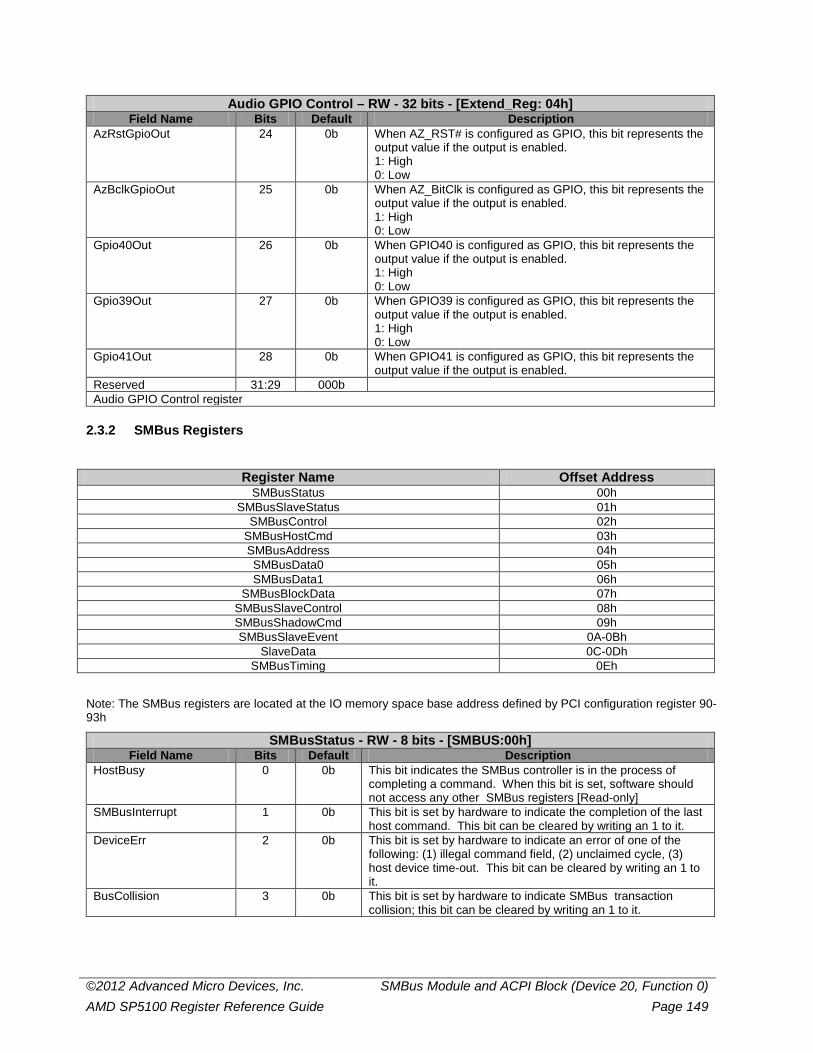
©2012 Advanced Micro Devices, Inc. SMBus Module and ACPI Block (Device 20, Function 0) AMD SP5100 Register Reference Guide Page 149
Audio GPIO Control – RW - 32 bits - [Extend_Reg: 04h] Field Name Bits Default Description
AzRstGpioOut 24 0b When AZ_RST# is configured as GPIO, this bit represents the output value if the output is enabled. 1: High 0: Low
AzBclkGpioOut 25 0b When AZ_BitClk is configured as GPIO, this bit represents the output value if the output is enabled. 1: High 0: Low
Gpio40Out 26 0b When GPIO40 is configured as GPIO, this bit represents the output value if the output is enabled. 1: High 0: Low
Gpio39Out 27 0b When GPIO39 is configured as GPIO, this bit represents the output value if the output is enabled. 1: High 0: Low
Gpio41Out 28 0b When GPIO41 is configured as GPIO, this bit represents the output value if the output is enabled.
Reserved 31:29 000b Audio GPIO Control register
2.3.2 SMBus Registers
Register Name Offset Address SMBusStatus 00h
SMBusSlaveStatus 01h SMBusControl 02h
SMBusHostCmd 03h SMBusAddress 04h SMBusData0 05h SMBusData1 06h
SMBusBlockData 07h SMBusSlaveControl 08h SMBusShadowCmd 09h SMBusSlaveEvent 0A-0Bh
SlaveData 0C-0Dh SMBusTiming 0Eh
Note: The SMBus registers are located at the IO memory space base address defined by PCI configuration register 90-93h
SMBusStatus - RW - 8 bits - [SMBUS:00h] Field Name Bits Default Description
HostBusy 0 0b This bit indicates the SMBus controller is in the process of completing a command. When this bit is set, software should not access any other SMBus registers [Read-only]
SMBusInterrupt 1 0b This bit is set by hardware to indicate the completion of the last host command. This bit can be cleared by writing an 1 to it.
DeviceErr 2 0b This bit is set by hardware to indicate an error of one of the following: (1) illegal command field, (2) unclaimed cycle, (3) host device time-out. This bit can be cleared by writing an 1 to it.
BusCollision 3 0b This bit is set by hardware to indicate SMBus transaction collision; this bit can be cleared by writing an 1 to it.
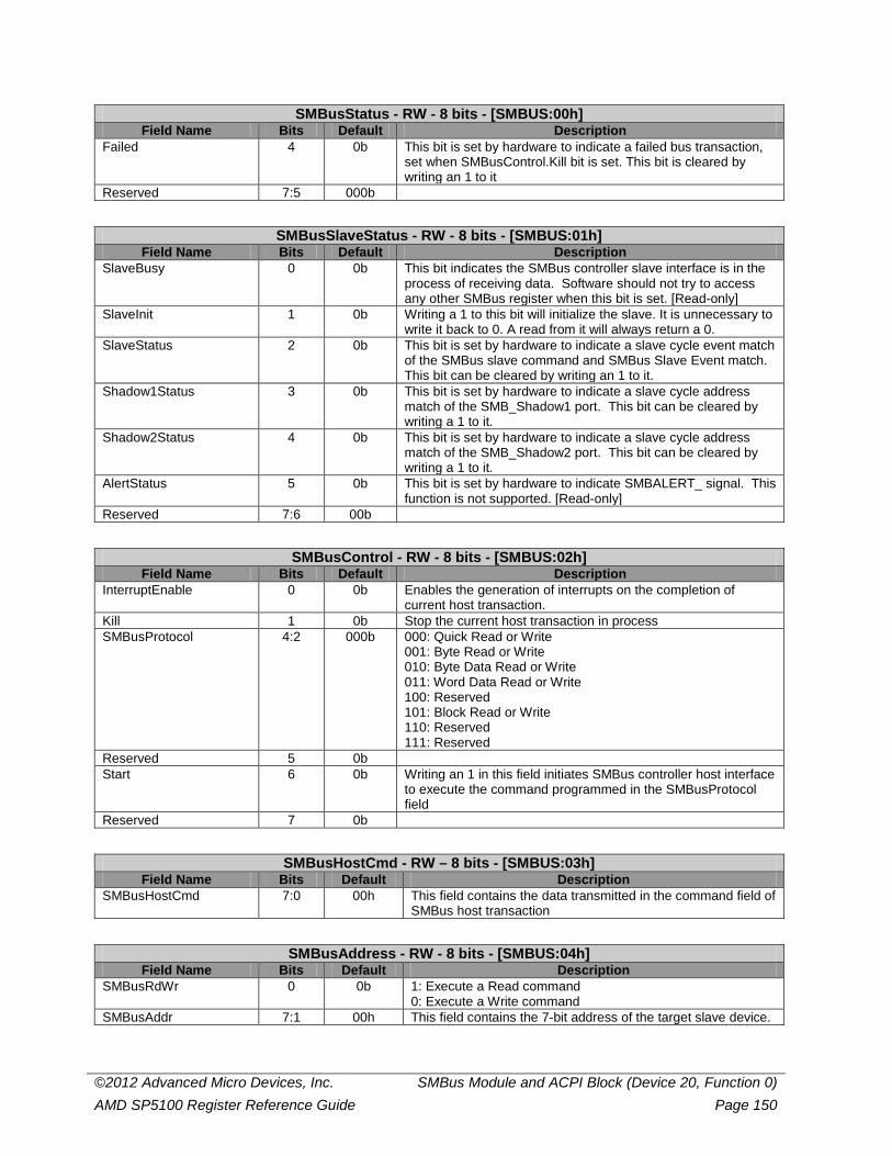
©2012 Advanced Micro Devices, Inc. SMBus Module and ACPI Block (Device 20, Function 0) AMD SP5100 Register Reference Guide Page 150
SMBusStatus - RW - 8 bits - [SMBUS:00h] Field Name Bits Default Description
Failed 4 0b This bit is set by hardware to indicate a failed bus transaction, set when SMBusControl.Kill bit is set. This bit is cleared by writing an 1 to it
Reserved 7:5 000b
SMBusSlaveStatus - RW - 8 bits - [SMBUS:01h] Field Name Bits Default Description
SlaveBusy 0 0b This bit indicates the SMBus controller slave interface is in the process of receiving data. Software should not try to access any other SMBus register when this bit is set. [Read-only]
SlaveInit 1 0b Writing a 1 to this bit will initialize the slave. It is unnecessary to write it back to 0. A read from it will always return a 0.
SlaveStatus 2 0b This bit is set by hardware to indicate a slave cycle event match of the SMBus slave command and SMBus Slave Event match. This bit can be cleared by writing an 1 to it.
Shadow1Status 3 0b This bit is set by hardware to indicate a slave cycle address match of the SMB_Shadow1 port. This bit can be cleared by writing a 1 to it.
Shadow2Status 4 0b This bit is set by hardware to indicate a slave cycle address match of the SMB_Shadow2 port. This bit can be cleared by writing a 1 to it.
AlertStatus 5 0b This bit is set by hardware to indicate SMBALERT_ signal. This function is not supported. [Read-only]
Reserved 7:6 00b
SMBusControl - RW - 8 bits - [SMBUS:02h] Field Name Bits Default Description
InterruptEnable 0 0b Enables the generation of interrupts on the completion of current host transaction.
Kill 1 0b Stop the current host transaction in process SMBusProtocol 4:2 000b 000: Quick Read or Write
001: Byte Read or Write 010: Byte Data Read or Write 011: Word Data Read or Write 100: Reserved 101: Block Read or Write 110: Reserved 111: Reserved
Reserved 5 0b Start 6 0b Writing an 1 in this field initiates SMBus controller host interface
to execute the command programmed in the SMBusProtocol field
Reserved 7 0b
SMBusHostCmd - RW – 8 bits - [SMBUS:03h] Field Name Bits Default Description
SMBusHostCmd 7:0 00h This field contains the data transmitted in the command field of SMBus host transaction
SMBusAddress - RW - 8 bits - [SMBUS:04h] Field Name Bits Default Description
SMBusRdWr 0 0b 1: Execute a Read command 0: Execute a Write command
SMBusAddr 7:1 00h This field contains the 7-bit address of the target slave device.
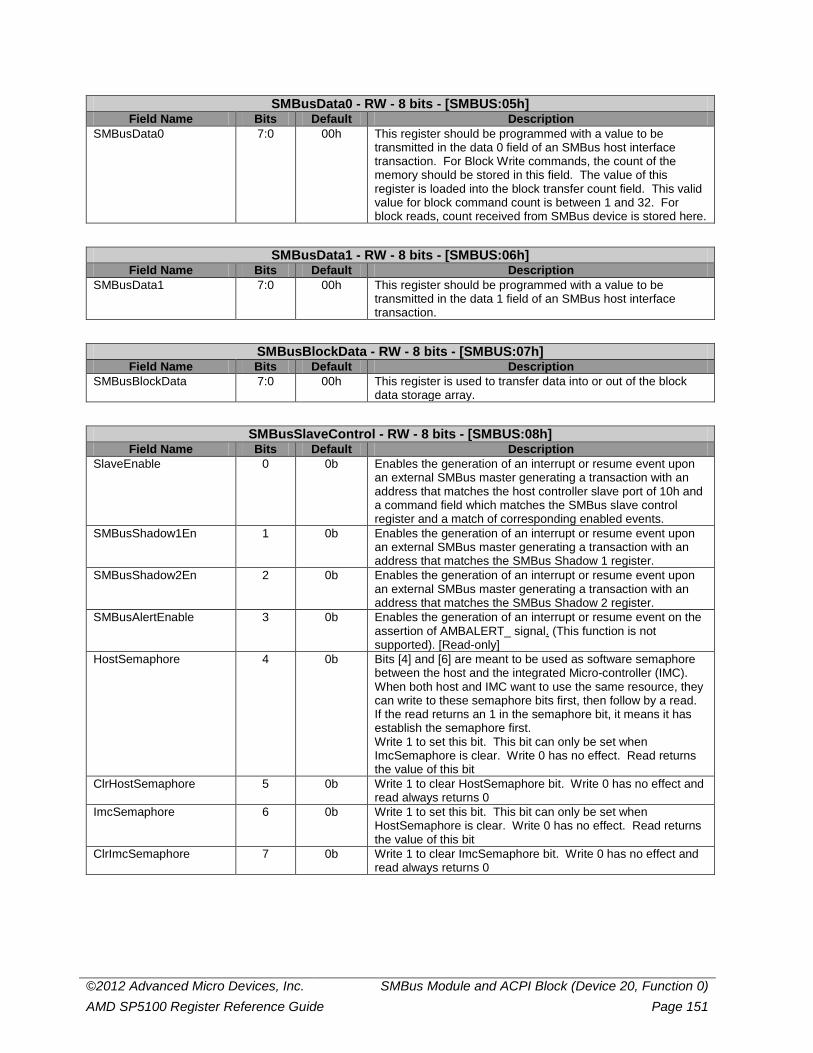
©2012 Advanced Micro Devices, Inc. SMBus Module and ACPI Block (Device 20, Function 0) AMD SP5100 Register Reference Guide Page 151
SMBusData0 - RW - 8 bits - [SMBUS:05h] Field Name Bits Default Description
SMBusData0 7:0 00h This register should be programmed with a value to be transmitted in the data 0 field of an SMBus host interface transaction. For Block Write commands, the count of the memory should be stored in this field. The value of this register is loaded into the block transfer count field. This valid value for block command count is between 1 and 32. For block reads, count received from SMBus device is stored here.
SMBusData1 - RW - 8 bits - [SMBUS:06h] Field Name Bits Default Description
SMBusData1 7:0 00h This register should be programmed with a value to be transmitted in the data 1 field of an SMBus host interface transaction.
SMBusBlockData - RW - 8 bits - [SMBUS:07h] Field Name Bits Default Description
SMBusBlockData 7:0 00h This register is used to transfer data into or out of the block data storage array.
SMBusSlaveControl - RW - 8 bits - [SMBUS:08h] Field Name Bits Default Description
SlaveEnable 0 0b Enables the generation of an interrupt or resume event upon an external SMBus master generating a transaction with an address that matches the host controller slave port of 10h and a command field which matches the SMBus slave control register and a match of corresponding enabled events.
SMBusShadow1En 1 0b Enables the generation of an interrupt or resume event upon an external SMBus master generating a transaction with an address that matches the SMBus Shadow 1 register.
SMBusShadow2En 2 0b Enables the generation of an interrupt or resume event upon an external SMBus master generating a transaction with an address that matches the SMBus Shadow 2 register.
SMBusAlertEnable 3 0b Enables the generation of an interrupt or resume event on the assertion of AMBALERT_ signal. (This function is not supported). [Read-only]
HostSemaphore 4 0b Bits [4] and [6] are meant to be used as software semaphore between the host and the integrated Micro-controller (IMC). When both host and IMC want to use the same resource, they can write to these semaphore bits first, then follow by a read. If the read returns an 1 in the semaphore bit, it means it has establish the semaphore first. Write 1 to set this bit. This bit can only be set when ImcSemaphore is clear. Write 0 has no effect. Read returns the value of this bit
ClrHostSemaphore 5 0b Write 1 to clear HostSemaphore bit. Write 0 has no effect and read always returns 0
ImcSemaphore 6 0b Write 1 to set this bit. This bit can only be set when HostSemaphore is clear. Write 0 has no effect. Read returns the value of this bit
ClrImcSemaphore 7 0b Write 1 to clear ImcSemaphore bit. Write 0 has no effect and read always returns 0
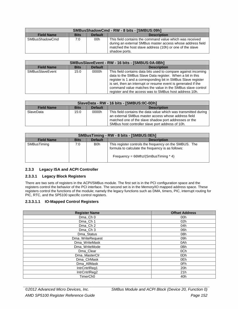
©2012 Advanced Micro Devices, Inc. SMBus Module and ACPI Block (Device 20, Function 0) AMD SP5100 Register Reference Guide Page 152
SMBusShadowCmd - RW - 8 bits - [SMBUS:09h] Field Name Bits Default Description
SMBusShadowCmd 7:0 00h This field contains the command value which was received during an external SMBus master access whose address field matched the host slave address (10h) or one of the slave shadow ports.
SMBusSlaveEvent - RW - 16 bits - [SMBUS:0A-0Bh] Field Name Bits Default Description
SMBusSlaveEvent 15:0 0000h This field contains data bits used to compare against incoming data to the SMBus Slave Data register. When a bit in this register is 1 and a corresponding bit in SMBus Slave register is set, then an interrupt or resume event is generated if the command value matches the value in the SMBus slave control register and the access was to SMBus host address 10h.
SlaveData - RW - 16 bits - [SMBUS:0C-0Dh] Field Name Bits Default Description
SlaveData 15:0 0000h This field contains the data value which was transmitted during an external SMBus master access whose address field matched one of the slave shadow port addresses or the SMBus host controller slave port address of 10h.
SMBusTiming - RW - 8 bits - [SMBUS:0Eh] Field Name Bits Default Description
SMBusTiming 7:0 B0h This register controls the frequency on the SMBUS. The formula to calculate the frequency is as follows: Frequency = 66Mhz/(SmBusTiming * 4)
2.3.3 Legacy ISA and ACPI Controller
2.3.3.1 Legacy Block Registers There are two sets of registers in the ACPI/SMBus module. The first set is in the PCI configuration space and the registers control the behavior of the PCI interface. The second set is in the Memory/IO mapped address space. These registers control the functions of the module; namely the legacy functions such as DMA, timers, PIC, interrupt routing for PIC, RTC, and the SP5100 specific control registers.
2.3.3.1.1 IO-Mapped Control Registers
Register Name Offset Address Dma_Ch 0 00h Dma_Ch 1 02h Dma_Ch 2 04h Dma_Ch 3 06h
Dma_Status 08h Dma_WriteRequest 09h
Dma_WriteMask 0Ah Dma_WriteMode 0Bh
Dma_Clear 0Ch Dma_MasterClr 0Dh Dma_ClrMask 0Eh Dma_AllMask 0Fh IntrCntrlReg1 20h IntrCntrlReg2 21h
TimerCh0 40h

©2012 Advanced Micro Devices, Inc. SMBus Module and ACPI Block (Device 20, Function 0) AMD SP5100 Register Reference Guide Page 153
Register Name Offset Address TimerCh1 41h TimerCh2 42h
Tmr1CntrlWord 43h Nmi_Status 61h Nmi_Enable 70h RtcDataPort 71h
AlternatRtcAddrPort 72h AlternatRtcDataPort 73h
Dma_PageCh2 81h Dma_PageCh3 82h Dma_PageCh1 83h
Dma_Page_Reserved1 84h Dma_Page_Reserved2 85h Dma_Page_Reserved3 86h
Dma_PageCh0 87h Dma_Page_Reserved4 88h
Dma_PageCh6 89h Dma_PageCh7 8Ah Dma_PageCh5 8Bh
Dma_Page_Reserved5 8Ch Dma_Page_Reserved6 8Dh Dma_Page_Reserved7 8Eh
Dma_Refresh 8Fh FastInit 92h
IntrCntrl2Reg1 A0h IntrCntrl2Reg2 A1h
Dma2_Ch4Addr C0h Dma2_Ch4Cnt C2h
Dma2_Ch5Addr C4h Dma2_Ch5Cnt C6h
Dma2_Ch6Addr C8h Dma2_Ch6Cnt CAh
Dma2_Ch7Addr CCh Dma2_Ch7Cnt CEh
Dma_Status D0h Dma_WriteRequest D2h
Dma_WriteMask D4h Dma_WriteMode D6h
Dma_Clear D8h Dma_Clear DAh
Dma_ClrMask DCh Dma_ClrMask DEh
NCP_Error F0h DMA1_Extend 40Bh IntrEdgeControl 4D0h DMA2_Extend 4D6h Pci_Intr_Index C00h Pci_Intr_Data C01h
Pci_Error C14h CMIndex C50h CMData C51h GpmPort C52h Isa_Misc C6Fh
PM2_Index CD0h PM2_Data CD1h
BIOSRAM_Index CD4h BIOSRAM_Data CD5h
PM_Index CD6h
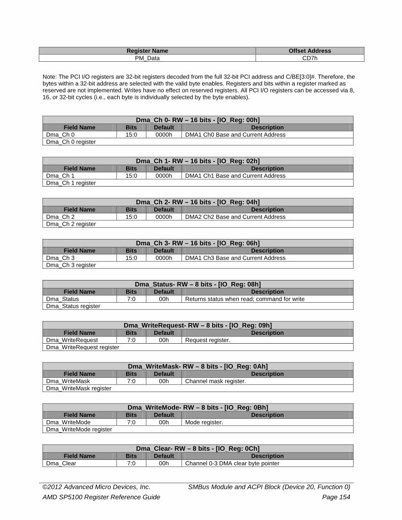
©2012 Advanced Micro Devices, Inc. SMBus Module and ACPI Block (Device 20, Function 0) AMD SP5100 Register Reference Guide Page 154
Register Name Offset Address PM_Data CD7h
Note: The PCI I/O registers are 32-bit registers decoded from the full 32-bit PCI address and C/BE[3:0]#. Therefore, the bytes within a 32-bit address are selected with the valid byte enables. Registers and bits within a register marked as reserved are not implemented. Writes have no effect on reserved registers. All PCI I/O registers can be accessed via 8, 16, or 32-bit cycles (i.e., each byte is individually selected by the byte enables).
Dma_Ch 0- RW – 16 bits - [IO_Reg: 00h] Field Name Bits Default Description
Dma_Ch 0 15:0 0000h DMA1 Ch0 Base and Current Address Dma_Ch 0 register
Dma_Ch 1- RW – 16 bits - [IO_Reg: 02h] Field Name Bits Default Description
Dma_Ch 1 15:0 0000h DMA1 Ch1 Base and Current Address Dma_Ch 1 register
Dma_Ch 2- RW – 16 bits - [IO_Reg: 04h] Field Name Bits Default Description
Dma_Ch 2 15:0 0000h DMA2 Ch2 Base and Current Address Dma_Ch 2 register
Dma_Ch 3- RW – 16 bits - [IO_Reg: 06h] Field Name Bits Default Description
Dma_Ch 3 15:0 0000h DMA1 Ch3 Base and Current Address Dma_Ch 3 register
Dma_Status- RW – 8 bits - [IO_Reg: 08h] Field Name Bits Default Description
Dma_Status 7:0 00h Returns status when read; command for write Dma_Status register
Dma_WriteRequest- RW – 8 bits - [IO_Reg: 09h] Field Name Bits Default Description
Dma_WriteRequest 7:0 00h Request register. Dma_WriteRequest register
Dma_WriteMask- RW – 8 bits - [IO_Reg: 0Ah] Field Name Bits Default Description
Dma_WriteMask 7:0 00h Channel mask register. Dma_WriteMask register
Dma_WriteMode- RW – 8 bits - [IO_Reg: 0Bh] Field Name Bits Default Description
Dma_WriteMode 7:0 00h Mode register. Dma_WriteMode register
Dma_Clear- RW – 8 bits - [IO_Reg: 0Ch] Field Name Bits Default Description
Dma_Clear 7:0 00h Channel 0-3 DMA clear byte pointer
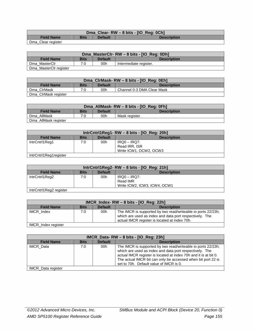
©2012 Advanced Micro Devices, Inc. SMBus Module and ACPI Block (Device 20, Function 0) AMD SP5100 Register Reference Guide Page 155
Dma_Clear- RW – 8 bits - [IO_Reg: 0Ch] Field Name Bits Default Description
Dma_Clear register
Dma_MasterClr- RW – 8 bits - [IO_Reg: 0Dh] Field Name Bits Default Description
Dma_MasterClr 7:0 00h Intermediate register. Dma_MasterClr register
Dma_ClrMask- RW – 8 bits - [IO_Reg: 0Eh] Field Name Bits Default Description
Dma_ClrMask 7:0 00h Channel 0-3 DMA Clear Mask Dma_ClrMask register
Dma_AllMask- RW – 8 bits - [IO_Reg: 0Fh] Field Name Bits Default Description
Dma_AllMask 7:0 00h Mask register. Dma_AllMask register
IntrCntrl1Reg1- RW – 8 bits - [IO_Reg: 20h] Field Name Bits Default Description
IntrCntrl1Reg1 7:0 00h IRQ0 – IRQ7: Read IRR, ISR Write ICW1, OCW2, OCW3
IntrCntrl1Reg1register
IntrCntrl1Reg2- RW – 8 bits - [IO_Reg: 21h] Field Name Bits Default Description
IntrCntrl1Reg2 7:0 00h IRQ0 – IRQ7: Read IMR Write ICW2, ICW3, ICW4, OCW1
IntrCntrl1Reg2 register
IMCR_Index- RW – 8 bits - [IO_Reg: 22h] Field Name Bits Default Description
IMCR_Index 7:0 00h The IMCR is supported by two read/writeable io ports 22/23h; which are used as index and data port respectively. The actual IMCR register is located at index 70h.
IMCR_Index register
IMCR_Data- RW – 8 bits - [IO_Reg: 23h] Field Name Bits Default Description
IMCR_Data 7:0 00h The IMCR is supported by two read/writeable io ports 22/23h; which are used as index and data port respectively. The actual IMCR register is located at index 70h and it is at bit 0. The actual IMCR bit can only be accessed when bit port 22 is set to 70h. Default value of IMCR is 0.
IMCR_Data register
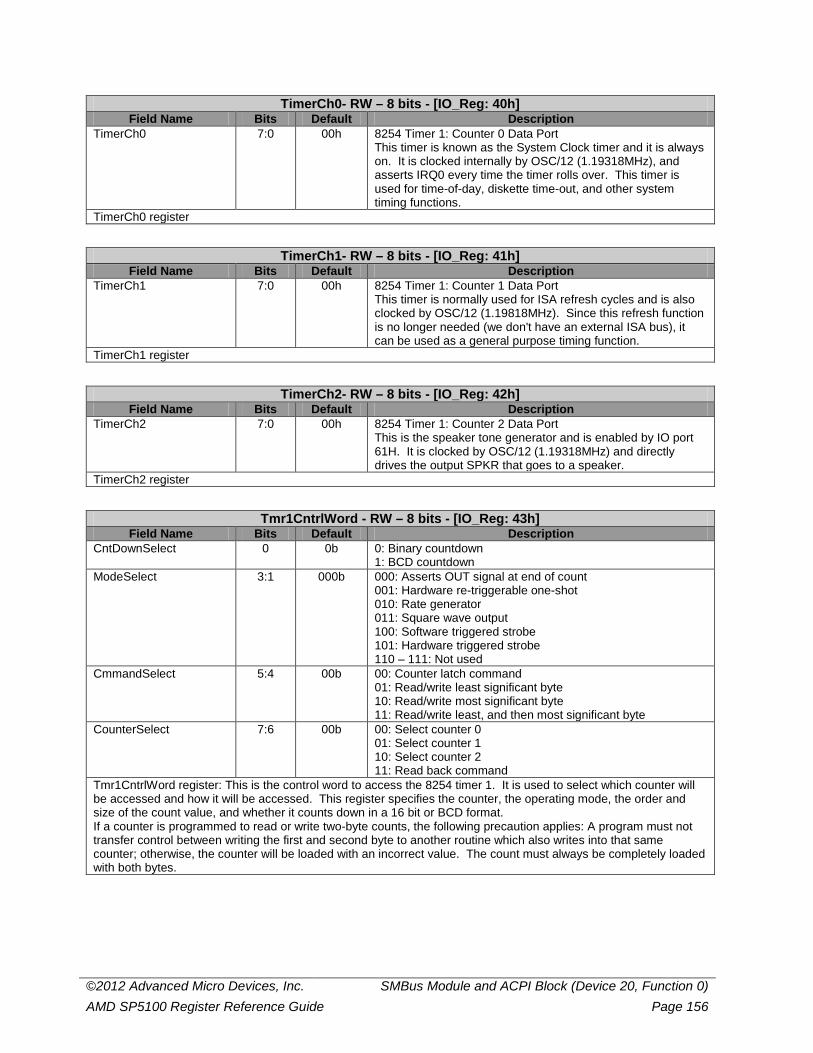
©2012 Advanced Micro Devices, Inc. SMBus Module and ACPI Block (Device 20, Function 0) AMD SP5100 Register Reference Guide Page 156
TimerCh0- RW – 8 bits - [IO_Reg: 40h] Field Name Bits Default Description
TimerCh0 7:0 00h 8254 Timer 1: Counter 0 Data Port This timer is known as the System Clock timer and it is always on. It is clocked internally by OSC/12 (1.19318MHz), and asserts IRQ0 every time the timer rolls over. This timer is used for time-of-day, diskette time-out, and other system timing functions.
TimerCh0 register
TimerCh1- RW – 8 bits - [IO_Reg: 41h] Field Name Bits Default Description
TimerCh1 7:0 00h 8254 Timer 1: Counter 1 Data Port This timer is normally used for ISA refresh cycles and is also clocked by OSC/12 (1.19818MHz). Since this refresh function is no longer needed (we don't have an external ISA bus), it can be used as a general purpose timing function.
TimerCh1 register
TimerCh2- RW – 8 bits - [IO_Reg: 42h] Field Name Bits Default Description
TimerCh2 7:0 00h 8254 Timer 1: Counter 2 Data Port This is the speaker tone generator and is enabled by IO port 61H. It is clocked by OSC/12 (1.19318MHz) and directly drives the output SPKR that goes to a speaker.
TimerCh2 register
Tmr1CntrlWord - RW – 8 bits - [IO_Reg: 43h] Field Name Bits Default Description
CntDownSelect 0 0b 0: Binary countdown 1: BCD countdown
ModeSelect 3:1 000b 000: Asserts OUT signal at end of count 001: Hardware re-triggerable one-shot 010: Rate generator 011: Square wave output 100: Software triggered strobe 101: Hardware triggered strobe 110 – 111: Not used
CmmandSelect 5:4 00b 00: Counter latch command 01: Read/write least significant byte 10: Read/write most significant byte 11: Read/write least, and then most significant byte
CounterSelect 7:6 00b 00: Select counter 0 01: Select counter 1 10: Select counter 2 11: Read back command
Tmr1CntrlWord register: This is the control word to access the 8254 timer 1. It is used to select which counter will be accessed and how it will be accessed. This register specifies the counter, the operating mode, the order and size of the count value, and whether it counts down in a 16 bit or BCD format. If a counter is programmed to read or write two-byte counts, the following precaution applies: A program must not transfer control between writing the first and second byte to another routine which also writes into that same counter; otherwise, the counter will be loaded with an incorrect value. The count must always be completely loaded with both bytes.
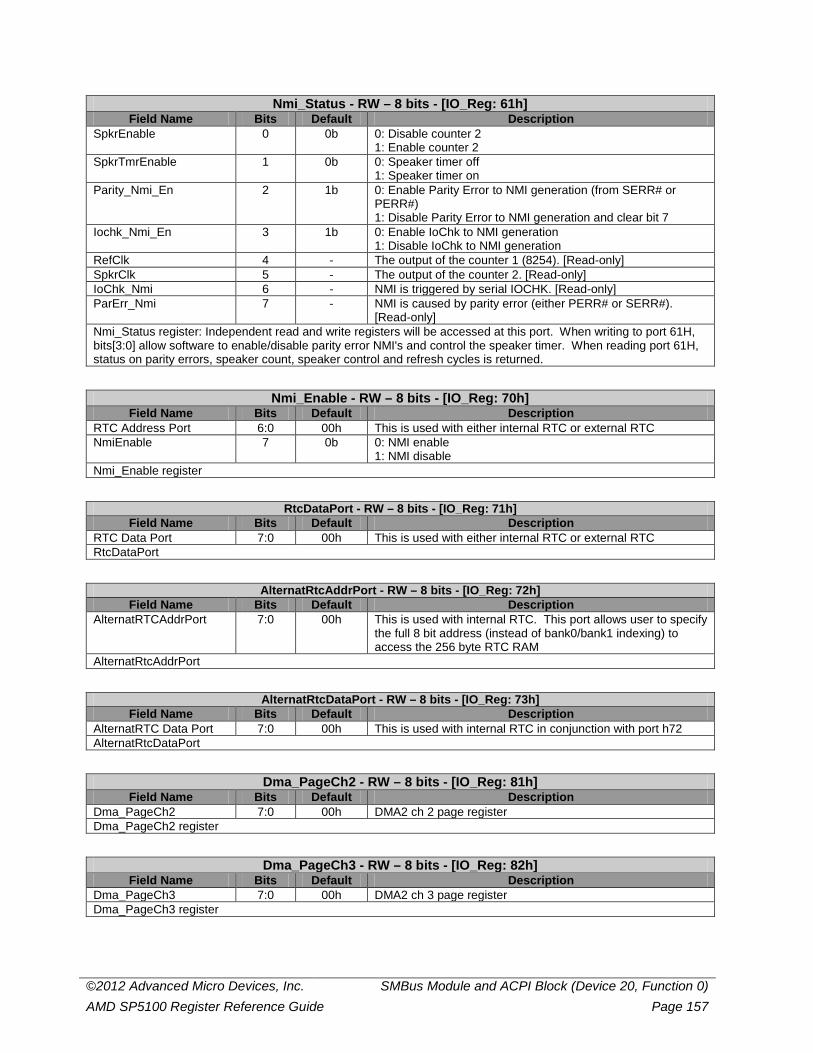
©2012 Advanced Micro Devices, Inc. SMBus Module and ACPI Block (Device 20, Function 0) AMD SP5100 Register Reference Guide Page 157
Nmi_Status - RW – 8 bits - [IO_Reg: 61h] Field Name Bits Default Description
SpkrEnable 0 0b 0: Disable counter 2 1: Enable counter 2
SpkrTmrEnable 1 0b 0: Speaker timer off 1: Speaker timer on
Parity_Nmi_En 2 1b 0: Enable Parity Error to NMI generation (from SERR# or PERR#) 1: Disable Parity Error to NMI generation and clear bit 7
Iochk_Nmi_En 3 1b 0: Enable IoChk to NMI generation 1: Disable IoChk to NMI generation
RefClk 4 - The output of the counter 1 (8254). [Read-only] SpkrClk 5 - The output of the counter 2. [Read-only] IoChk_Nmi 6 - NMI is triggered by serial IOCHK. [Read-only] ParErr_Nmi 7 - NMI is caused by parity error (either PERR# or SERR#).
[Read-only] Nmi_Status register: Independent read and write registers will be accessed at this port. When writing to port 61H, bits[3:0] allow software to enable/disable parity error NMI's and control the speaker timer. When reading port 61H, status on parity errors, speaker count, speaker control and refresh cycles is returned.
Nmi_Enable - RW – 8 bits - [IO_Reg: 70h] Field Name Bits Default Description
RTC Address Port 6:0 00h This is used with either internal RTC or external RTC NmiEnable 7 0b 0: NMI enable
1: NMI disable Nmi_Enable register
RtcDataPort - RW – 8 bits - [IO_Reg: 71h] Field Name Bits Default Description
RTC Data Port 7:0 00h This is used with either internal RTC or external RTC RtcDataPort
AlternatRtcAddrPort - RW – 8 bits - [IO_Reg: 72h] Field Name Bits Default Description
AlternatRTCAddrPort 7:0 00h This is used with internal RTC. This port allows user to specify the full 8 bit address (instead of bank0/bank1 indexing) to access the 256 byte RTC RAM
AlternatRtcAddrPort
AlternatRtcDataPort - RW – 8 bits - [IO_Reg: 73h] Field Name Bits Default Description
AlternatRTC Data Port 7:0 00h This is used with internal RTC in conjunction with port h72 AlternatRtcDataPort
Dma_PageCh2 - RW – 8 bits - [IO_Reg: 81h] Field Name Bits Default Description
Dma_PageCh2 7:0 00h DMA2 ch 2 page register Dma_PageCh2 register
Dma_PageCh3 - RW – 8 bits - [IO_Reg: 82h] Field Name Bits Default Description
Dma_PageCh3 7:0 00h DMA2 ch 3 page register Dma_PageCh3 register
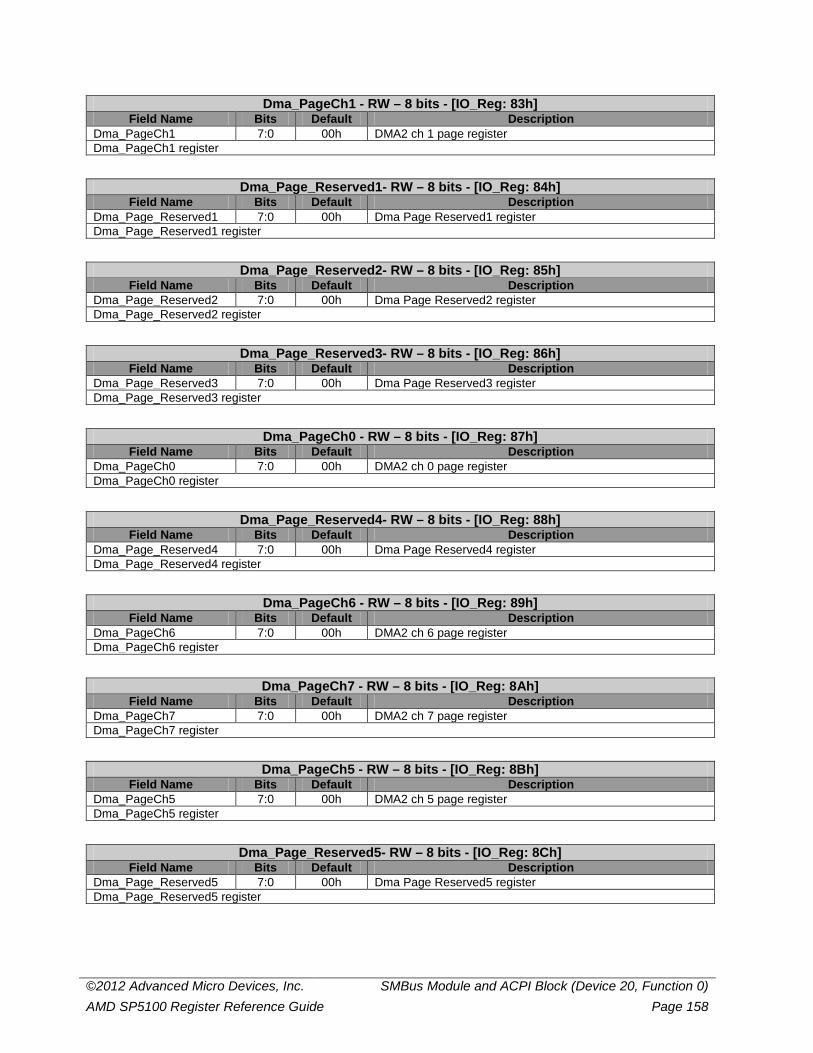
©2012 Advanced Micro Devices, Inc. SMBus Module and ACPI Block (Device 20, Function 0) AMD SP5100 Register Reference Guide Page 158
Dma_PageCh1 - RW – 8 bits - [IO_Reg: 83h] Field Name Bits Default Description
Dma_PageCh1 7:0 00h DMA2 ch 1 page register Dma_PageCh1 register
Dma_Page_Reserved1- RW – 8 bits - [IO_Reg: 84h] Field Name Bits Default Description
Dma_Page_Reserved1 7:0 00h Dma Page Reserved1 register Dma_Page_Reserved1 register
Dma_Page_Reserved2- RW – 8 bits - [IO_Reg: 85h] Field Name Bits Default Description
Dma_Page_Reserved2 7:0 00h Dma Page Reserved2 register Dma_Page_Reserved2 register
Dma_Page_Reserved3- RW – 8 bits - [IO_Reg: 86h] Field Name Bits Default Description
Dma_Page_Reserved3 7:0 00h Dma Page Reserved3 register Dma_Page_Reserved3 register
Dma_PageCh0 - RW – 8 bits - [IO_Reg: 87h] Field Name Bits Default Description
Dma_PageCh0 7:0 00h DMA2 ch 0 page register Dma_PageCh0 register
Dma_Page_Reserved4- RW – 8 bits - [IO_Reg: 88h] Field Name Bits Default Description
Dma_Page_Reserved4 7:0 00h Dma Page Reserved4 register Dma_Page_Reserved4 register
Dma_PageCh6 - RW – 8 bits - [IO_Reg: 89h] Field Name Bits Default Description
Dma_PageCh6 7:0 00h DMA2 ch 6 page register Dma_PageCh6 register
Dma_PageCh7 - RW – 8 bits - [IO_Reg: 8Ah] Field Name Bits Default Description
Dma_PageCh7 7:0 00h DMA2 ch 7 page register Dma_PageCh7 register
Dma_PageCh5 - RW – 8 bits - [IO_Reg: 8Bh] Field Name Bits Default Description
Dma_PageCh5 7:0 00h DMA2 ch 5 page register Dma_PageCh5 register
Dma_Page_Reserved5- RW – 8 bits - [IO_Reg: 8Ch] Field Name Bits Default Description
Dma_Page_Reserved5 7:0 00h Dma Page Reserved5 register Dma_Page_Reserved5 register
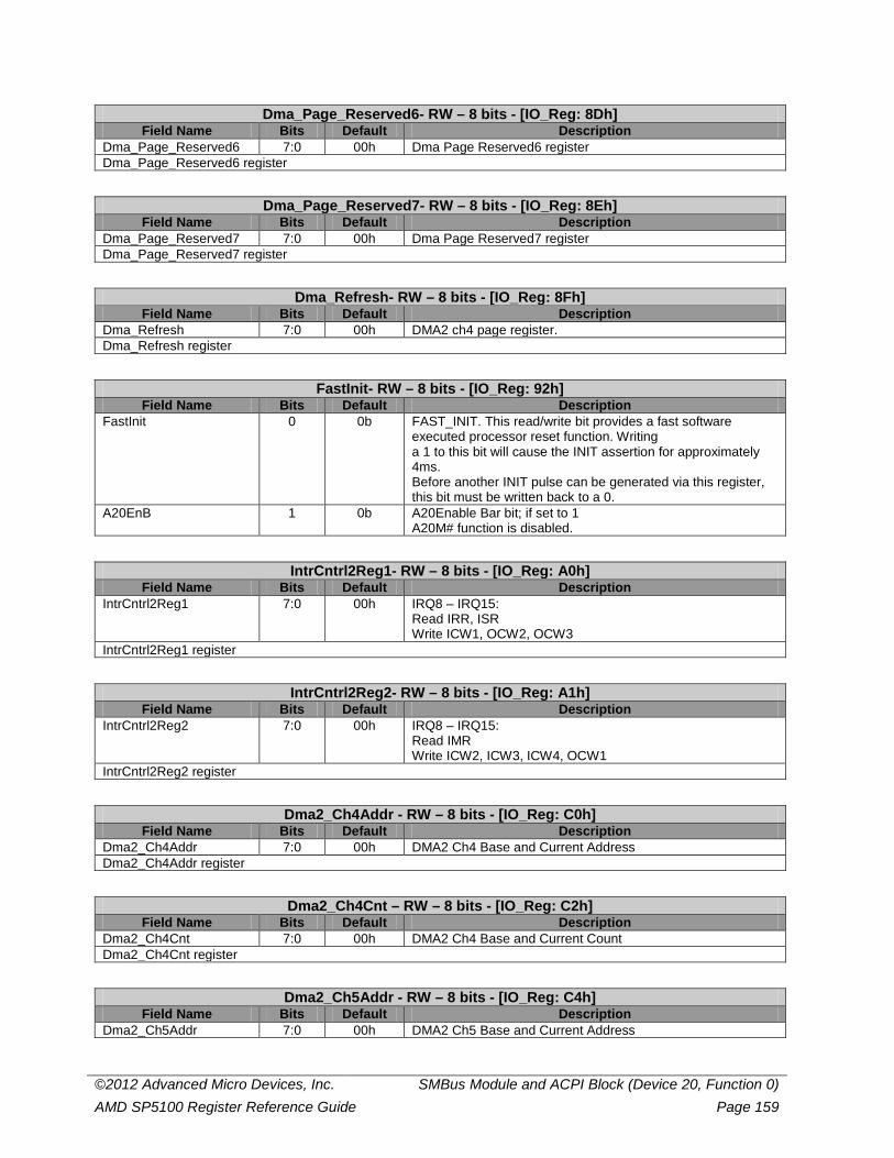
©2012 Advanced Micro Devices, Inc. SMBus Module and ACPI Block (Device 20, Function 0) AMD SP5100 Register Reference Guide Page 159
Dma_Page_Reserved6- RW – 8 bits - [IO_Reg: 8Dh] Field Name Bits Default Description
Dma_Page_Reserved6 7:0 00h Dma Page Reserved6 register Dma_Page_Reserved6 register
Dma_Page_Reserved7- RW – 8 bits - [IO_Reg: 8Eh] Field Name Bits Default Description
Dma_Page_Reserved7 7:0 00h Dma Page Reserved7 register Dma_Page_Reserved7 register
Dma_Refresh- RW – 8 bits - [IO_Reg: 8Fh] Field Name Bits Default Description
Dma_Refresh 7:0 00h DMA2 ch4 page register. Dma_Refresh register
FastInit- RW – 8 bits - [IO_Reg: 92h] Field Name Bits Default Description
FastInit 0 0b FAST_INIT. This read/write bit provides a fast software executed processor reset function. Writing a 1 to this bit will cause the INIT assertion for approximately 4ms. Before another INIT pulse can be generated via this register, this bit must be written back to a 0.
A20EnB 1 0b A20Enable Bar bit; if set to 1 A20M# function is disabled.
IntrCntrl2Reg1- RW – 8 bits - [IO_Reg: A0h] Field Name Bits Default Description
IntrCntrl2Reg1 7:0 00h IRQ8 – IRQ15: Read IRR, ISR Write ICW1, OCW2, OCW3
IntrCntrl2Reg1 register
IntrCntrl2Reg2- RW – 8 bits - [IO_Reg: A1h] Field Name Bits Default Description
IntrCntrl2Reg2 7:0 00h IRQ8 – IRQ15: Read IMR Write ICW2, ICW3, ICW4, OCW1
IntrCntrl2Reg2 register
Dma2_Ch4Addr - RW – 8 bits - [IO_Reg: C0h] Field Name Bits Default Description
Dma2_Ch4Addr 7:0 00h DMA2 Ch4 Base and Current Address Dma2_Ch4Addr register
Dma2_Ch4Cnt – RW – 8 bits - [IO_Reg: C2h] Field Name Bits Default Description
Dma2_Ch4Cnt 7:0 00h DMA2 Ch4 Base and Current Count Dma2_Ch4Cnt register
Dma2_Ch5Addr - RW – 8 bits - [IO_Reg: C4h] Field Name Bits Default Description
Dma2_Ch5Addr 7:0 00h DMA2 Ch5 Base and Current Address
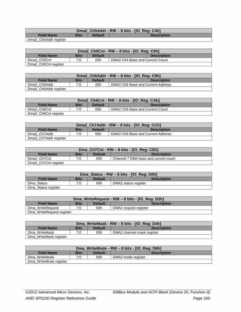
©2012 Advanced Micro Devices, Inc. SMBus Module and ACPI Block (Device 20, Function 0) AMD SP5100 Register Reference Guide Page 160
Dma2_Ch5Addr - RW – 8 bits - [IO_Reg: C4h] Field Name Bits Default Description
Dma2_Ch5Addr register
Dma2_Ch5Cnt - RW – 8 bits - [IO_Reg: C6h] Field Name Bits Default Description
Dma2_Ch5Cnt 7:0 00h DMA2 Ch4 Base and Current Count Dma2_Ch5Cnt register
Dma2_Ch6Addr - RW – 8 bits - [IO_Reg: C8h] Field Name Bits Default Description
Dma2_Ch6Addr 7:0 00h DMA2 Ch6 Base and Current Address Dma2_Ch6Addr register
Dma2_Ch6Cnt - RW – 8 bits - [IO_Reg: CAh] Field Name Bits Default Description
Dma2_Ch6Cnt 7:0 00h DMA2 Ch6 Base and Current Count Dma2_Ch6Cnt register
Dma2_Ch7Addr - RW – 8 bits - [IO_Reg: CCh] Field Name Bits Default Description
Dma2_Ch7Addr 7:0 00h DMA2 Ch5 Base and Current Address Dma2_Ch7Addr register
Dma_Ch7Cnt - RW – 8 bits - [IO_Reg: CEh] Field Name Bits Default Description
Dma2_Ch7Cnt 7:0 00h Channel 7 DMA base and current count Dma2_Ch7Cnt register
Dma_Status - RW – 8 bits - [IO_Reg: D0h] Field Name Bits Default Description
Dma_Status 7:0 00h DMA2 status register Dma_Status register
Dma_WriteRequest - RW – 8 bits - [IO_Reg: D2h] Field Name Bits Default Description
Dma_WriteRequest 7:0 00h DMA2 request register Dma_WriteRequest register
Dma_WriteMask - RW – 8 bits - [IO_Reg: D4h] Field Name Bits Default Description
Dma_WriteMask 7:0 00h DMA2 channel mask register Dma_WriteMask register
Dma_WriteMode - RW – 8 bits - [IO_Reg: D6h] Field Name Bits Default Description
Dma_WriteMode 7:0 00h DMA2 mode register Dma_WriteMode register
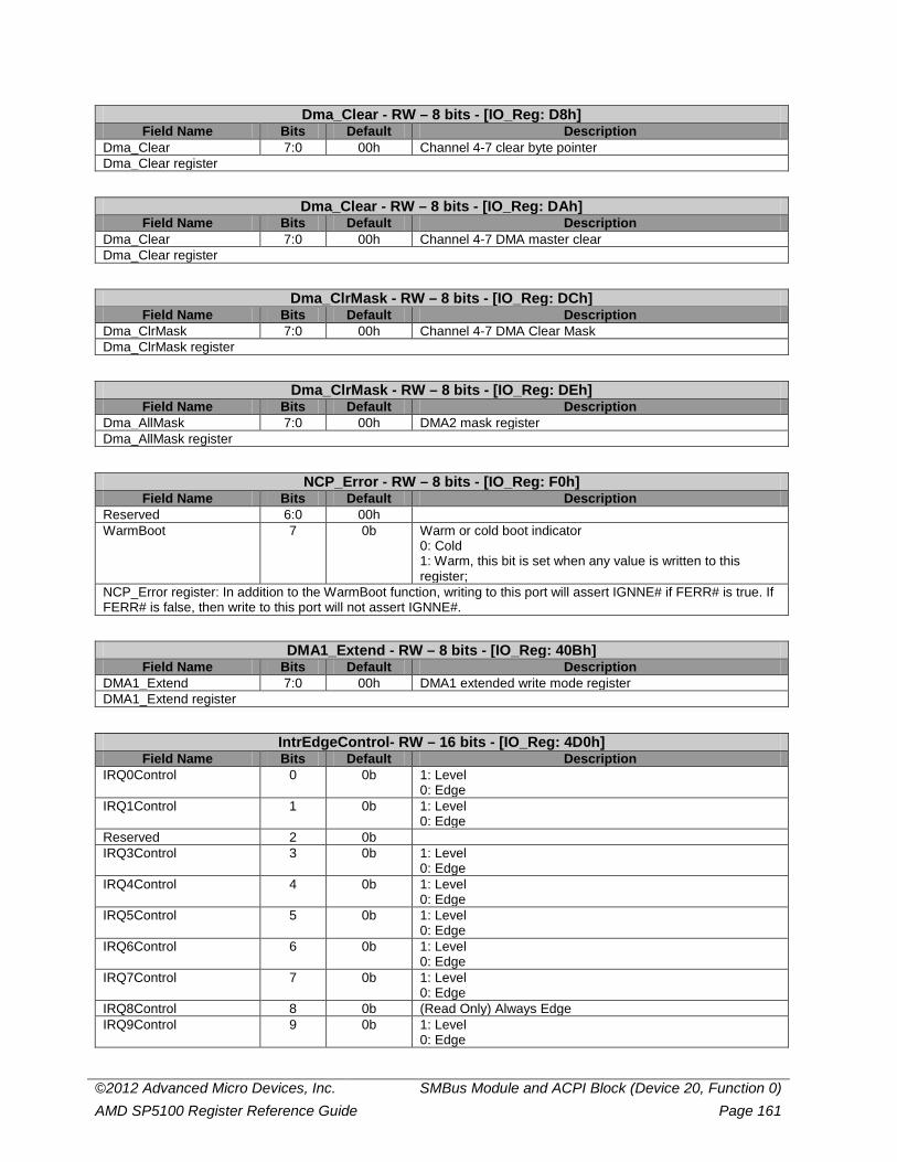
©2012 Advanced Micro Devices, Inc. SMBus Module and ACPI Block (Device 20, Function 0) AMD SP5100 Register Reference Guide Page 161
Dma_Clear - RW – 8 bits - [IO_Reg: D8h] Field Name Bits Default Description
Dma_Clear 7:0 00h Channel 4-7 clear byte pointer Dma_Clear register
Dma_Clear - RW – 8 bits - [IO_Reg: DAh] Field Name Bits Default Description
Dma_Clear 7:0 00h Channel 4-7 DMA master clear Dma_Clear register
Dma_ClrMask - RW – 8 bits - [IO_Reg: DCh] Field Name Bits Default Description
Dma_ClrMask 7:0 00h Channel 4-7 DMA Clear Mask Dma_ClrMask register
Dma_ClrMask - RW – 8 bits - [IO_Reg: DEh] Field Name Bits Default Description
Dma_AllMask 7:0 00h DMA2 mask register Dma_AllMask register
NCP_Error - RW – 8 bits - [IO_Reg: F0h] Field Name Bits Default Description
Reserved 6:0 00h WarmBoot 7 0b Warm or cold boot indicator
0: Cold 1: Warm, this bit is set when any value is written to this register;
NCP_Error register: In addition to the WarmBoot function, writing to this port will assert IGNNE# if FERR# is true. If FERR# is false, then write to this port will not assert IGNNE#.
DMA1_Extend - RW – 8 bits - [IO_Reg: 40Bh] Field Name Bits Default Description
DMA1_Extend 7:0 00h DMA1 extended write mode register DMA1_Extend register
IntrEdgeControl- RW – 16 bits - [IO_Reg: 4D0h] Field Name Bits Default Description
IRQ0Control 0 0b 1: Level 0: Edge
IRQ1Control 1 0b 1: Level 0: Edge
Reserved 2 0b IRQ3Control 3 0b 1: Level
0: Edge IRQ4Control 4 0b 1: Level
0: Edge IRQ5Control 5 0b 1: Level
0: Edge IRQ6Control 6 0b 1: Level
0: Edge IRQ7Control 7 0b 1: Level
0: Edge IRQ8Control 8 0b (Read Only) Always Edge IRQ9Control 9 0b 1: Level
0: Edge
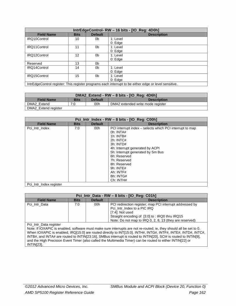
©2012 Advanced Micro Devices, Inc. SMBus Module and ACPI Block (Device 20, Function 0) AMD SP5100 Register Reference Guide Page 162
IntrEdgeControl- RW – 16 bits - [IO_Reg: 4D0h] Field Name Bits Default Description
IRQ10Control 10 0b 1: Level 0: Edge
IRQ11Control 11 0b 1: Level 0: Edge
IRQ12Control 12 0b 1: Level 0: Edge
Reserved 13 0b IRQ14Control 14 0b 1: Level
0: Edge IRQ15Control 15 0b 1: Level
0: Edge IntrEdgeControl register: This register programs each interrupt to be either edge or level sensitive.
DMA2_Extend - RW – 8 bits - [IO_Reg: 4D6h] Field Name Bits Default Description
DMA2_Extend 7:0 00h DMA2 extended write mode register DMA2_Extend register
Pci_Intr_Index - RW – 8 bits - [IO_Reg: C00h] Field Name Bits Default Description
Pci_Intr_Index 7:0 00h PCI interrupt index – selects which PCI interrupt to map 0h: INTA# 1h: INTB# 2h: INTC# 3h: INTD# 4h: Interrupt generated by ACPI 5h: Interrupt generated by Sm Bus 6h: Reserved 7h: Reserved 8h: Reserved 9h: INTE# Ah: INTF# Bh: INTG# Ch: INTH#
Pci_Intr_Index register
Pci_Intr_Data - RW – 8 bits - [IO_Reg: C01h] Field Name Bits Default Description
Pci_Intr_Data 7:0 00h PCI redirection register; map PCI interrupt addressed by Pci_Intr_Index to a PIC IRQ [7:4]: Not used Straight encoding of [3:0] to : IRQ0 thru IRQ15 Note: Do not map to IRQ 0, 2, 8, 13 (they are reserved)
Pci_Intr_Data register Note: If IOXAPIC is enabled, software must make sure interrupts are not re-routed; ie, they should all be set to 0. When IOXAPIC is enabled, IRQ[15:0] are routed directly to INT[15:0]. INTH#, INTG#, INTF#, INTE#, INTD#, INTC#, INTB#, and INTA# are routed to INTIN[23:16], SMBus interrupt is routed to INTIN[20], SCI# is routed to INTIN[9], and the High Precision Event Timer (also called the Multimedia Timer) can be routed to either INTIN[22] or INTIN[23].
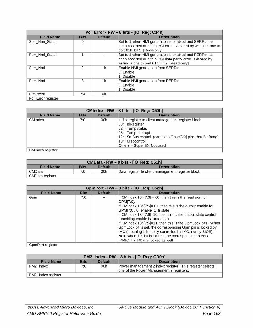
©2012 Advanced Micro Devices, Inc. SMBus Module and ACPI Block (Device 20, Function 0) AMD SP5100 Register Reference Guide Page 163
Pci_Error - RW – 8 bits - [IO_Reg: C14h] Field Name Bits Default Description
Serr_Nmi_Status 0 - Set to 1 when NMI generation is enabled and SERR# has been asserted due to a PCI error. Cleared by writing a one to port 61h, bit 2. [Read-only]
Perr_Nmi_Status 1 - Set to 1 when NMI generation is enabled and PERR# has been asserted due to a PCI data parity error. Cleared by writing a one to port 61h, bit 2. [Read-only]
Serr_Nmi 2 1b Enable NMI generation from SERR# 0: Enable 1: Disable
Perr_Nmi 3 1b Enable NMI generation from PERR# 0: Enable 1: Disable
Reserved 7:4 0h Pci_Error register
CMIndex - RW – 8 bits - [IO_Reg: C50h] Field Name Bits Default Description
CMIndex 7:0 00h Index register to client management register block 00h: IdRegister 02h: TempStatus 03h: TempInterrupt 12h: SmBus control (control to Gpoc[3:0] pins thru Bit Bang) 13h: Misccontrol Others – Super IO: Not used
CMIndex register
CMData - RW – 8 bits - [IO_Reg: C51h] Field Name Bits Default Description
CMData 7:0 00h Data register to client management register block CMData register
GpmPort - RW – 8 bits - [IO_Reg: C52h] Field Name Bits Default Description
Gpm 7:0 -- If CMIndex.13h[7:6] = 00, then this is the read port for GPM[7:0]. If CMIndex.13h[7:6]= 01, then this is the output enable for GPM[7:0], 0=enable, 1=tristate If CMIndex.13h[7:6]=10, then this is the output state control (providing enable is turned on) If CMIndex 13h[7:6]=11, then this is the GpmLock bits. When GpmLock bit is set, the corresponding Gpm pin is locked by IMC (meaning it is solely controlled by IMC; not by BIOS). Note when this bit is locked, the corresponding PU/PD (PMIO_F7:F6) are lcoked as well
GpmPort register
PM2_Index - RW – 8 bits - [IO_Reg: CD0h] Field Name Bits Default Description
PM2_Index 7:0 00h Power management 2 index register. This register selects one of the Power Management 2 registers.
PM2_Index register
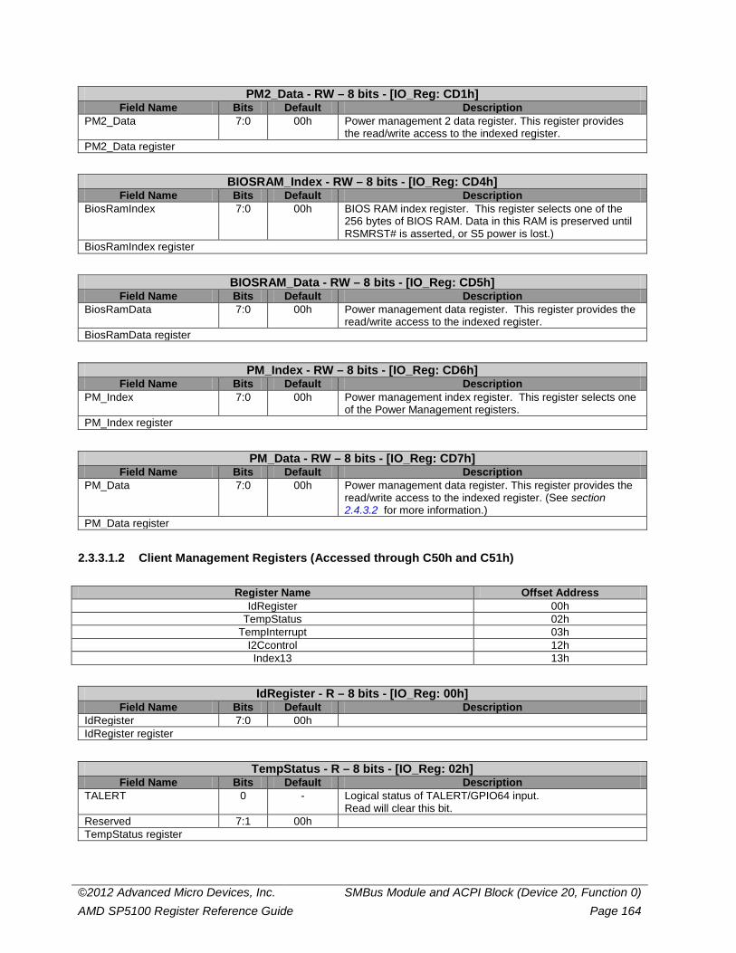
©2012 Advanced Micro Devices, Inc. SMBus Module and ACPI Block (Device 20, Function 0) AMD SP5100 Register Reference Guide Page 164
PM2_Data - RW – 8 bits - [IO_Reg: CD1h] Field Name Bits Default Description
PM2_Data 7:0 00h Power management 2 data register. This register provides the read/write access to the indexed register.
PM2_Data register
BIOSRAM_Index - RW – 8 bits - [IO_Reg: CD4h] Field Name Bits Default Description
BiosRamIndex 7:0 00h BIOS RAM index register. This register selects one of the 256 bytes of BIOS RAM. Data in this RAM is preserved until RSMRST# is asserted, or S5 power is lost.)
BiosRamIndex register
BIOSRAM_Data - RW – 8 bits - [IO_Reg: CD5h] Field Name Bits Default Description
BiosRamData 7:0 00h Power management data register. This register provides the read/write access to the indexed register.
BiosRamData register
PM_Index - RW – 8 bits - [IO_Reg: CD6h] Field Name Bits Default Description
PM_Index 7:0 00h Power management index register. This register selects one of the Power Management registers.
PM_Index register
PM_Data - RW – 8 bits - [IO_Reg: CD7h] Field Name Bits Default Description
PM_Data 7:0 00h Power management data register. This register provides the read/write access to the indexed register. (See section 2.4.3.2 for more information.)
PM_Data register
2.3.3.1.2 Client Management Registers (Accessed through C50h and C51h)
Register Name Offset Address IdRegister 00h
TempStatus 02h TempInterrupt 03h
I2Ccontrol 12h Index13 13h
IdRegister - R – 8 bits - [IO_Reg: 00h] Field Name Bits Default Description
IdRegister 7:0 00h IdRegister register
TempStatus - R – 8 bits - [IO_Reg: 02h] Field Name Bits Default Description
TALERT 0 - Logical status of TALERT/GPIO64 input. Read will clear this bit.
Reserved 7:1 00h TempStatus register
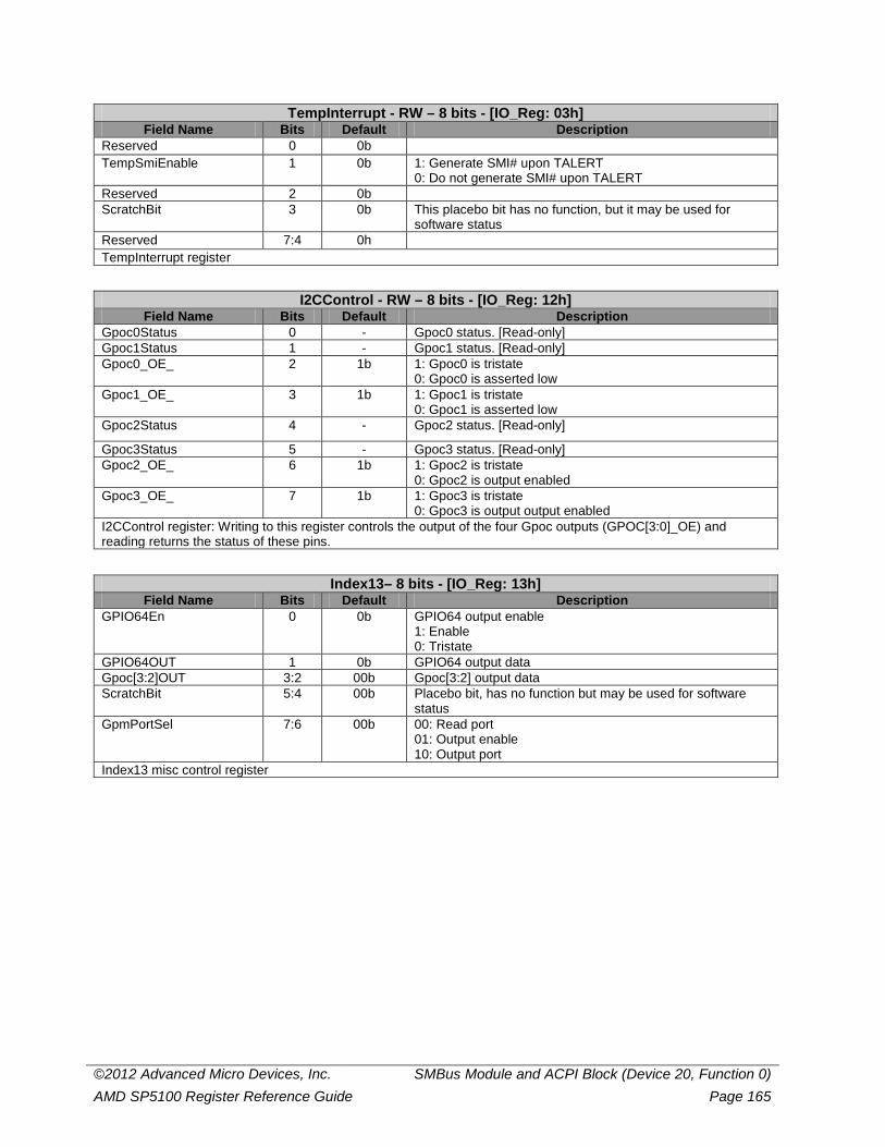
©2012 Advanced Micro Devices, Inc. SMBus Module and ACPI Block (Device 20, Function 0) AMD SP5100 Register Reference Guide Page 165
TempInterrupt - RW – 8 bits - [IO_Reg: 03h] Field Name Bits Default Description
Reserved 0 0b TempSmiEnable 1 0b 1: Generate SMI# upon TALERT
0: Do not generate SMI# upon TALERT Reserved 2 0b ScratchBit 3 0b This placebo bit has no function, but it may be used for
software status Reserved 7:4 0h TempInterrupt register
I2CControl - RW – 8 bits - [IO_Reg: 12h] Field Name Bits Default Description
Gpoc0Status 0 - Gpoc0 status. [Read-only] Gpoc1Status 1 - Gpoc1 status. [Read-only] Gpoc0_OE_ 2 1b 1: Gpoc0 is tristate
0: Gpoc0 is asserted low Gpoc1_OE_ 3 1b 1: Gpoc1 is tristate
0: Gpoc1 is asserted low Gpoc2Status 4 - Gpoc2 status. [Read-only]
Gpoc3Status 5 - Gpoc3 status. [Read-only] Gpoc2_OE_ 6 1b 1: Gpoc2 is tristate
0: Gpoc2 is output enabled Gpoc3_OE_ 7 1b 1: Gpoc3 is tristate
0: Gpoc3 is output output enabled I2CControl register: Writing to this register controls the output of the four Gpoc outputs (GPOC[3:0]_OE) and reading returns the status of these pins.
Index13– 8 bits - [IO_Reg: 13h] Field Name Bits Default Description
GPIO64En 0 0b GPIO64 output enable 1: Enable 0: Tristate
GPIO64OUT 1 0b GPIO64 output data Gpoc[3:2]OUT 3:2 00b Gpoc[3:2] output data ScratchBit 5:4 00b Placebo bit, has no function but may be used for software
status GpmPortSel 7:6 00b 00: Read port
01: Output enable 10: Output port
Index13 misc control register

©2012 Advanced Micro Devices, Inc. SMBus Module and ACPI Block (Device 20, Function 0) AMD SP5100 Register Reference Guide Page 166
2.3.3.1.3 System Reset Register (IO CF9) Note: Refer to PM IO reg x85 for a detailed description. This register has been designed to be dual-port accessable.
2.3.3.2 Power Management (PM) Registers The power management (PM) block is resident in the PCI/LPC/ISA bridge. The PM registers are accessed via IO mapped registers xCD6h and xCD7h. The index address is first programmed into IO register xCD6h. Read or write values are accessed through IO register xCD7h.
Register Name Offset Address MiscControl 00h MiscStatus 01h
SmiWakeUpEventEnable1 02h SmiWakeUpEventEnable2 03h SmiWakeUpEventEnable3 04h SmiWakeUpEventStatus1 05h SmiWakeUpEventStatus2 06h SmiWakeUpEventStatus3 07h InactiveTmrEventEnable1 08h InactiveTmrEventEnable2 09h InactiveTmrEventEnable3 0Ah
PmTmr1InitValue 0Bh PmTmr1CurValue 0Ch PwrLedExtEvent 0Dh PwrLedExtEvent 0Eh
AcpiStatus 0Fh AcpiEn 10h
MiscEnable11 11h PmTmr2InitValue 12h PmTmr2CurValue 13h
Programlo0RangeLo 14h Programlo0RangeHi 15h ProgramIo1RangeLo 16h ProgramIo1RangeHi 17h ProgramIo2RangeLo 18h ProgramIo2RangeHi 19h ProgramIo3RangeLo 1Ah ProgramIo3RangeHi 1Bh
ProgramIoEnable 1Ch IOMonitorStatus 1Dh
InactiveTmrEventEnable4 1Eh AcpiPm1EvtBlkLo 20h AcpiPm1EvtBlkHi 21h AcpiPm1CntBlkLo 22h AcpiPm1CntBlkHi 23h AcpiPmTmrBlkLo 24h AcpiPmTmrBlkHi 25h
CpuControlLo 26h CpuControlHi 27h
AcpiGpe0BlkLo 28h AcpiGpe0BlkHi 29h AcpiSmiCmdLo 2Ah AcpiSmiCmdHi 2Bh
AcpiPm2CntBlkLo 2Ch AcpiPm2CntBlkHi 2Dh
GEvtConfig0 30h GEvtConfig1 31h

©2012 Advanced Micro Devices, Inc. SMBus Module and ACPI Block (Device 20, Function 0) AMD SP5100 Register Reference Guide Page 167
Register Name Offset Address GPMConfig0 32h GPMConfig1 33h GPMConfig2 34h GPMConfig3 35h
GEvtLevelConfig 36h GPMLevelConfig0 37h GPMLevelConfig1 38h
GEvtStatus 39h PMEStatus0 3Ah PMEStatus1 3Bh OthersConfig 3Ch
VRT_T1 3Eh VRT_T2 3Fh
AD_Pull_UpB 40h PM_Enable 50h TPRESET1 51h TPRESET2 52h
TESTENABLE 53h PWRBTTN_CLR 54h
SoftPciRst 55h Reserved 56h Reserved 57h Reserved 58h
MiscOption 59h SmiSciSts0 5Ah SmiSciSts1 5Bh SmiSciSts2 5Ch SmiSciSts3 5Dh
Software NMI 5Eh Reserved 5Fh Options_0 60h Options_1 61h
Shadow_SCI 62h SwitchVoltageTime 63h SwitchGHI_Time 64h UsbPMControl 65h MiscEnable66 66h MiscEnable67 67h MiscEnable68 68h
WatchDogTimerControl 69h WatchDogTimerBase0 6Ch WatchDogTimerBase1 6Dh WatchDogTimerBase2 6Eh WatchDogTimerBase3 6Fh
S_LdtStartTime 70h EnhanceOption 71h PopUpEndTime 73h PwrFailShadow 74h
Tpreset1b 75h SOS3ToS5Enable0 76h SOS3ToS5Enable1 77h SOS3ToS5Enable2 78h SOS3ToS5Enable3 79h NoStatusControl0 7Ah NoStatusControl1 7Bh
MiscEnable7C 7Ch DprSlpVrMinTime 7Dh
SMAF0 80h

©2012 Advanced Micro Devices, Inc. SMBus Module and ACPI Block (Device 20, Function 0) AMD SP5100 Register Reference Guide Page 168
Register Name Offset Address SMAF1 81h SMAF2 82h SMAF3 83h
WakePinCntl 84h CF9Rst 85h
ThermThrotCntl 86h LdtStpCmd 87h
LdtStartTime 88h LdtStopDelay 89h
LdtAgpTimeCntl 8Ah StutterTime 8Bh
StpClkDlyTime 8Ch AbPmeCntl 8Dh
FakeAsr 8Eh FakeAsrEn 8Fh
GEVENTOUT 90h GEVENTEN 91h GEVENTIN 92h GPM98OUT 94h GPM98EN 95h GPM98IN 96h
EnhanceControl 9Ah MsiSignature 9E:9Ch
AutoArbDisWaitTime 9Fh Programlo4RangeLo A0h Programlo4RangeHi A1h Programlo5RangeLo A2h Programlo5RangeHi A3h Programlo6RangeLo A4h Programlo6RangeHi A5h Programlo7RangeLo A6h Programlo7RangeHi A7h
PIO7654Enable A8h PIO7654Status A9h
StrapStatus B2:B0h C2Count B3h C3Count B4h
IMC_ASF_Fan_Temp_Enable B6h IMC_Volt_Enable B7h
IMC_GroupA_Enable B8h IMC_GroupB_Enable B9h IMC_SMBus_Enable BAh IMC_ACPI_Enable BBh
FC_Clk_Sel BCh SysClkCfg1 BD
SmiIndicator0 C0h SmiIndicator1 C1h SmiIndicator2 C2h
PostCode C3h ClkbufDrvStr_A C4h ClkbufDrvStr_B C5h ClkbufDrvStr_C C6h
Spare C7h HT_TestControl C8h MultiK8Control C9h ClkPinControl CAh
AltStrapControl CBh EpromStrapIndex CCh
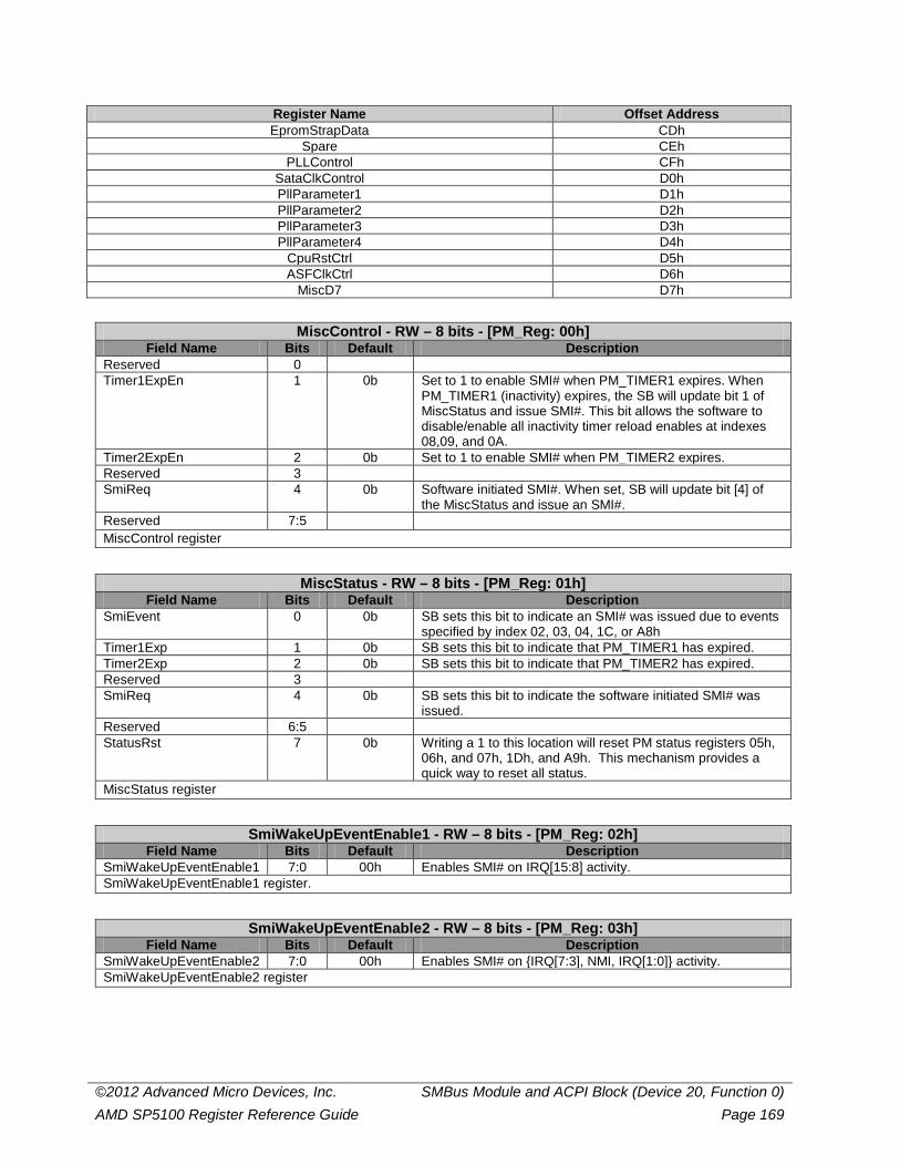
©2012 Advanced Micro Devices, Inc. SMBus Module and ACPI Block (Device 20, Function 0) AMD SP5100 Register Reference Guide Page 169
Register Name Offset Address EpromStrapData CDh
Spare CEh PLLControl CFh
SataClkControl D0h PllParameter1 D1h PllParameter2 D2h PllParameter3 D3h PllParameter4 D4h
CpuRstCtrl D5h ASFClkCtrl D6h
MiscD7 D7h
MiscControl - RW – 8 bits - [PM_Reg: 00h] Field Name Bits Default Description
Reserved 0 Timer1ExpEn 1 0b Set to 1 to enable SMI# when PM_TIMER1 expires. When
PM_TIMER1 (inactivity) expires, the SB will update bit 1 of MiscStatus and issue SMI#. This bit allows the software to disable/enable all inactivity timer reload enables at indexes 08,09, and 0A.
Timer2ExpEn 2 0b Set to 1 to enable SMI# when PM_TIMER2 expires. Reserved 3 SmiReq 4 0b Software initiated SMI#. When set, SB will update bit [4] of
the MiscStatus and issue an SMI#. Reserved 7:5 MiscControl register
MiscStatus - RW – 8 bits - [PM_Reg: 01h] Field Name Bits Default Description
SmiEvent 0 0b SB sets this bit to indicate an SMI# was issued due to events specified by index 02, 03, 04, 1C, or A8h
Timer1Exp 1 0b SB sets this bit to indicate that PM_TIMER1 has expired. Timer2Exp 2 0b SB sets this bit to indicate that PM_TIMER2 has expired. Reserved 3 SmiReq 4 0b SB sets this bit to indicate the software initiated SMI# was
issued. Reserved 6:5 StatusRst 7 0b Writing a 1 to this location will reset PM status registers 05h,
06h, and 07h, 1Dh, and A9h. This mechanism provides a quick way to reset all status.
MiscStatus register
SmiWakeUpEventEnable1 - RW – 8 bits - [PM_Reg: 02h] Field Name Bits Default Description
SmiWakeUpEventEnable1 7:0 00h Enables SMI# on IRQ[15:8] activity. SmiWakeUpEventEnable1 register.
SmiWakeUpEventEnable2 - RW – 8 bits - [PM_Reg: 03h] Field Name Bits Default Description
SmiWakeUpEventEnable2 7:0 00h Enables SMI# on {IRQ[7:3], NMI, IRQ[1:0]} activity. SmiWakeUpEventEnable2 register
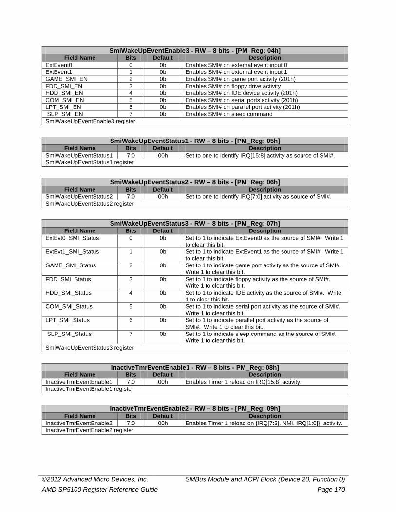
©2012 Advanced Micro Devices, Inc. SMBus Module and ACPI Block (Device 20, Function 0) AMD SP5100 Register Reference Guide Page 170
SmiWakeUpEventEnable3 - RW – 8 bits - [PM_Reg: 04h] Field Name Bits Default Description
ExtEvent0 0 0b Enables SMI# on external event input 0 ExtEvent1 1 0b Enables SMI# on external event input 1 GAME_SMI_EN 2 0b Enables SMI# on game port activity (201h) FDD_SMI_EN 3 0b Enables SMI# on floppy drive activity HDD_SMI_EN 4 0b Enables SMI# on IDE device activity (201h) COM_SMI_EN 5 0b Enables SMI# on serial ports activity (201h) LPT_SMI_EN 6 0b Enables SMI# on parallel port activity (201h) SLP_SMI_EN 7 0b Enables SMI# on sleep command SmiWakeUpEventEnable3 register.
SmiWakeUpEventStatus1 - RW – 8 bits - [PM_Reg: 05h] Field Name Bits Default Description
SmiWakeUpEventStatus1 7:0 00h Set to one to identify IRQ[15:8] activity as source of SMI#. SmiWakeUpEventStatus1 register
SmiWakeUpEventStatus2 - RW – 8 bits - [PM_Reg: 06h] Field Name Bits Default Description
SmiWakeUpEventStatus2 7:0 00h Set to one to identify IRQ[7:0] activity as source of SMI#. SmiWakeUpEventStatus2 register
SmiWakeUpEventStatus3 - RW – 8 bits - [PM_Reg: 07h] Field Name Bits Default Description
ExtEvt0_SMI_Status 0 0b Set to 1 to indicate ExtEvent0 as the source of SMI#. Write 1 to clear this bit.
ExtEvt1_SMI_Status 1 0b Set to 1 to indicate ExtEvent1 as the source of SMI#. Write 1 to clear this bit.
GAME_SMI_Status 2 0b Set to 1 to indicate game port activity as the source of SMI#. Write 1 to clear this bit.
FDD_SMI_Status 3 0b Set to 1 to indicate floppy activity as the source of SMI#. Write 1 to clear this bit.
HDD_SMI_Status 4 0b Set to 1 to indicate IDE activity as the source of SMI#. Write 1 to clear this bit.
COM_SMI_Status 5 0b Set to 1 to indicate serial port activity as the source of SMI#. Write 1 to clear this bit.
LPT_SMI_Status 6 0b Set to 1 to indicate parallel port activity as the source of SMI#. Write 1 to clear this bit.
SLP_SMI_Status 7 0b Set to 1 to indicate sleep command as the source of SMI#. Write 1 to clear this bit.
SmiWakeUpEventStatus3 register
InactiveTmrEventEnable1 - RW – 8 bits - PM_Reg: 08h] Field Name Bits Default Description
InactiveTmrEventEnable1 7:0 00h Enables Timer 1 reload on IRQ[15:8] activity. InactiveTmrEventEnable1 register
InactiveTmrEventEnable2 - RW – 8 bits - [PM_Reg: 09h] Field Name Bits Default Description
InactiveTmrEventEnable2 7:0 00h Enables Timer 1 reload on {IRQ[7:3], NMI, IRQ[1:0]} activity. InactiveTmrEventEnable2 register

©2012 Advanced Micro Devices, Inc. SMBus Module and ACPI Block (Device 20, Function 0) AMD SP5100 Register Reference Guide Page 171
InactiveTmrEventEnable3 - RW – 8 bits - [PM_Reg: 0Ah] Field Name Bits Default Description
ExtEvt0_Timer1Enable 0 0b Enables Timer1 reload on ExtEvent0 inactivity ExtEvt1_Timer1Enable 1 0b Enables Timer1 reload on ExtEvent1 inactivity GamePort_Timer1Enable 2 0b Enables Timer1 reload on Gameport inactivity Floppy_Timer1Enable 3 0b Enables Timer1 reload on Floppy port inactivity IDE_Timer1Enable 4 0b Enables Timer1 reload on IDE port inactivity COM_Timer1Enable 5 0b Enables Timer1 reload on COM port inactivity Parallel_Timer1Enable 6 0b Enables Timer1 reload on Parallel port inactivity Reserved 7 InactiveTmrEventEnable3 register
PmTmr1InitValue - RW – 8 bits - [PM_Reg: 0Bh] Field Name Bits Default Description
PmTmr1InitValue 5:0 000000b 6 bit-timer. Initial/reload value for 6 bit decrementing counter. Count range from 1 minute to 64 minutes with 4 second accuracy.
Reserved 7:6 PmTmr1InitValue register
PmTmr1CurValue - R – 8 bits - [PM_Reg: 0Ch] Field Name Bits Default Description
PmTmr1CurValue 5:0 - Current value of decrementing counter Reserved 7:6 PmTmr1CurValue register
ExtEventCntrl - RW – 8 bits - [PM_Reg: 0Dh] Field Name Bits Default Description
ExtEvent0State 0 - Logical value of EXTEVENT0. [Read-only] ExtEvent1State 1 - Logical value of EXTEVENT1. [Read-only] ExtEvent0RF 2 0b Set to one to configure EXTEVENT0 as rising edge sensitive.
0 as falling edge sensitive ExtEvent1RF 3 0b Set to one to configure EXTEVENT1 as rising edge sensitive.
0 as falling edge sensitive Reserved 7:4 ExtEventCntrl register
AcpiControl - RW – 8 bits - [PM_Reg: 0Eh] Field Name Bits Default Description
AcpiSmiEn 0 0b Set to 1 to enable SMI# generation when ACPI driver writes one to GBL_RLS (bit [2] of AcpiPm1CntBlk:00h). When an SMI# is issued, the SB updates bit [0] of the AcpiStatus register.
BIOS_RLS 1 0b Writing 1 to this bit will cause GblStatus to be set. This bit is always read back as 0.
SmiCmdEn 2 0b Set to 1 to enable SMI# generation when ACPI driver writes to the SmiCmd port. When set to 1, SB will update bit 2 of MiscStatus and issue an SMI# on write to SmiCmd port.
AcpiDecodeEnable 3 0b Set to 1 to enable SB to decode the ACPI I/O address space. When set, SB uses the contents of the PM registers at index 20-2B to decode ACPI I/O address.
VRT_SMI_En 4 0b Set to 1 to enable SB to generate SMI upon (RTC) VRT low. Reserved 5 RtcClkPUB 6 0b This bit controls the integrated pull-up for RTCCLK
0: Enable 1: Disable
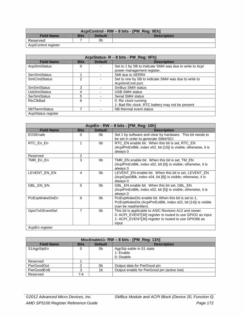
©2012 Advanced Micro Devices, Inc. SMBus Module and ACPI Block (Device 20, Function 0) AMD SP5100 Register Reference Guide Page 172
AcpiControl - RW – 8 bits - [PM_Reg: 0Eh] Field Name Bits Default Description
Reserved 7 0b AcpiControl register
AcpiStatus- R – 8 bits - PM_Reg: 0Fh] Field Name Bits Default Description
AcpiSmiStatus 0 - Set to 1 by SB to inidcate SMI# was due to write to Acpi power management register.
SerrSmiStatus 1 - SMI due to SERR# SmiCmdStatus 2 - Set to one by SB to indicate SMI# was due to write to
AcpiSmiCmd port. SmSmiStatus 3 - SmBus SMI# status UsbSmiStatus 4 - USB SMI# status SerSmiStatus 5 - Serial SMI# status RtcClkBad 6 - 0: Rtc clock running
1: Bad Rtc clock. RTC battery may not be present NbThermStatus 7 - NB thermal event status AcpiStatus register
AcpiEn - RW – 8 bits - [PM_Reg: 10h] Field Name Bits Default Description
EOSEnale 0 0b Set 1 by software and clear by hardware. This bit needs to be set in order to generate SMI#/SCI
RTC_En_En 1 0b RTC_EN enable bit. When this bit is set, RTC_EN (AcpiPmEvtBlk, index x02, bit [10]) is visible; otherwise, it is always 0
Reserved 2 TMR_En_En 3 0b TMR_EN enable bit. When this bit is set, TM_EN
(AcpiPmEvtBlk, index x02, bit [0]) is visible; otherwise, it is always 0
LEVENT_EN_EN 4 0b LEVENT_EN enable bit. When this bit is set, LEVENT_EN (AcpiGpe0Blk, index x04, bit [8]) is visible; otherwise, it is always 0
GBL_EN_EN 5 0b GBL_EN enable bit. When this bit set, GBL_EN (AcpiPmEvtBlk, index x02, bit [5]) is visible; otherwise, it is always 0
PciExpWakeDisEn 6 0b PciExpWakeDis enable bit. When this bit is set to 1, PciExpWakeDis (AcpiPmEvtBlk, index x02, bit [14]) is visible (can be read/written).
GpioToGEventSel 7 0b This bit is applicable to ASIC Revision A12 and newer. 0: ACPI_EVENT[30] register is routed to use GPIO2 as input 1: ACPI_EVENT[30] register is routed to use GPIO66 as input
AcpiEn register
MiscEnable11- RW – 8 bits - [PM_Reg: 11h] Field Name Bits Default Description
S1AgpStpEn 0 0b AgpStp eable in S1 state 1: Enable 0: Disable
Reserved 1 PwrGoodOut 2 0b Output data for PwrGood pin PwrGoodEnB 3 1b Output enable for PwrGood pin (active low) Reserved 7:4
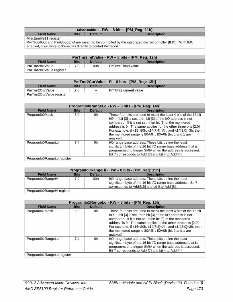
©2012 Advanced Micro Devices, Inc. SMBus Module and ACPI Block (Device 20, Function 0) AMD SP5100 Register Reference Guide Page 173
MiscEnable11- RW – 8 bits - [PM_Reg: 11h] Field Name Bits Default Description
MiscEnable11 register PwrGoodOut and PwrGoodEnB are meant to be controlled by the integrated micro-controller (IMC). With IMC enabled, it will write to these bits directly to control PwrGood
PmTmr2InitValue - RW – 8 bits - [PM_Reg: 12h] Field Name Bits Default Description
PmTmr2InitValue 7:0 00h PmTmr2 load value PmTmr2InitValue register
PmTmr2CurValue - R – 8 bits - [PM_Reg: 13h] Field Name Bits Default Description
PmTmr2CurValue 7:0 -- PmTmr2 current value PmTmr2CurValue register
Programlo0RangeLo - RW – 8 bits - [PM_Reg: 14h] Field Name Bits Default Description
ProgramIo0Mask 3:0 0h These four bits are used to mask the least 4 bits of the 16 bit I/O. If bit [3] is set, then bit [3] of the I/O address is not compared. If it is not set, then bit [3] of the monitored address is 0. The same applies for the other three bits [2:0]. For example, if x15=80h, x14[7:4]=Ah, and x14[3:0]=3h, then the monitored range is 80A4h : 80A0h (bit 0 and 1 are masked)
ProgramIo0RangeLo 7:4 0h I/O range base address. These bits define the least significant byte of the 16 bit I/O range base address that is programmed to trigger SMI# when the address is accessed. Bit 7 corresponds to Addr[7] and bit 4 to Addr[4].
ProgramIo0RangeLo register
ProgramIo0RangeHi - RW – 8 bits - [PM_Reg: 15h] Field Name Bits Default Description
ProgramIo0RangeHi 7:0 00h I/O range base address. These bits define the most significant byte of the 16 bit I/O range base address. Bit 7 corresponds to Addr[15] and bit 0 to Addr[8].
ProgramIo0RangeHi register
ProgramIo1RangeLo - RW – 8 bits - [PM_Reg: 16h] Field Name Bits Default Description
ProgramIo1Mask 3:0 0h These four bits are used to mask the least 4 bits of the 16 bit I/O. If bit [3] is set, then bit [3] of the I/O address is not compared. If it is not set, then bit [3] of the monitored address is 0. The same applies to the other three bits [2:0]. For example, if x15=80h, x14[7:4]=Ah, and x14[3:0]=3h, then the monitored range is 80A4h : 80A0h (bit 0 and 1 are masked)
ProgramI01RangeLo 7:4 0h I/O range base address. These bits define the least significant byte of the 16 bit I/O range base address that is programmed to trigger SMI# when the address is accessed. Bit 7 corresponds to Addr[7] and bit 4 to Addr[4].
ProgramIo1RangeLo register
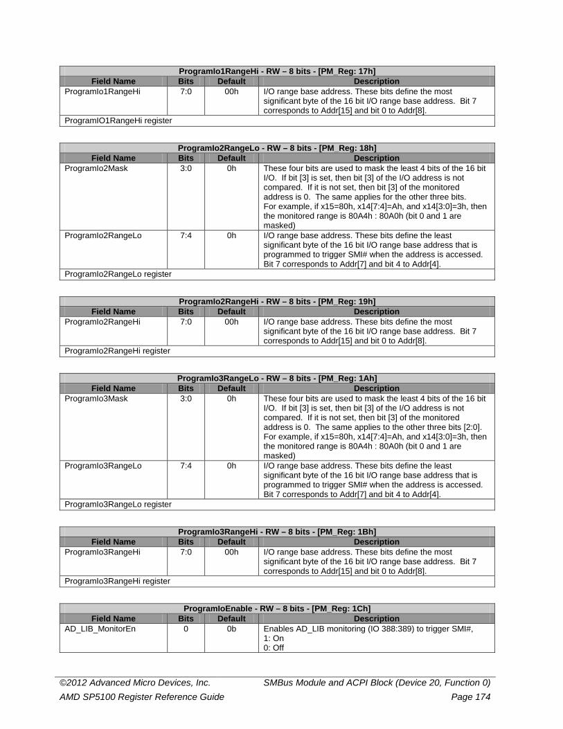
©2012 Advanced Micro Devices, Inc. SMBus Module and ACPI Block (Device 20, Function 0) AMD SP5100 Register Reference Guide Page 174
ProgramIo1RangeHi - RW – 8 bits - [PM_Reg: 17h] Field Name Bits Default Description
ProgramIo1RangeHi 7:0 00h I/O range base address. These bits define the most significant byte of the 16 bit I/O range base address. Bit 7 corresponds to Addr[15] and bit 0 to Addr[8].
ProgramIO1RangeHi register
ProgramIo2RangeLo - RW – 8 bits - [PM_Reg: 18h] Field Name Bits Default Description
ProgramIo2Mask 3:0 0h These four bits are used to mask the least 4 bits of the 16 bit I/O. If bit [3] is set, then bit [3] of the I/O address is not compared. If it is not set, then bit [3] of the monitored address is 0. The same applies for the other three bits. For example, if x15=80h, x14[7:4]=Ah, and x14[3:0]=3h, then the monitored range is 80A4h : 80A0h (bit 0 and 1 are masked)
ProgramIo2RangeLo 7:4 0h I/O range base address. These bits define the least significant byte of the 16 bit I/O range base address that is programmed to trigger SMI# when the address is accessed. Bit 7 corresponds to Addr[7] and bit 4 to Addr[4].
ProgramIo2RangeLo register
ProgramIo2RangeHi - RW – 8 bits - [PM_Reg: 19h] Field Name Bits Default Description
ProgramIo2RangeHi 7:0 00h I/O range base address. These bits define the most significant byte of the 16 bit I/O range base address. Bit 7 corresponds to Addr[15] and bit 0 to Addr[8].
ProgramIo2RangeHi register
ProgramIo3RangeLo - RW – 8 bits - [PM_Reg: 1Ah] Field Name Bits Default Description
ProgramIo3Mask 3:0 0h These four bits are used to mask the least 4 bits of the 16 bit I/O. If bit [3] is set, then bit [3] of the I/O address is not compared. If it is not set, then bit [3] of the monitored address is 0. The same applies to the other three bits [2:0]. For example, if x15=80h, x14[7:4]=Ah, and x14[3:0]=3h, then the monitored range is 80A4h : 80A0h (bit 0 and 1 are masked)
ProgramIo3RangeLo 7:4 0h I/O range base address. These bits define the least significant byte of the 16 bit I/O range base address that is programmed to trigger SMI# when the address is accessed. Bit 7 corresponds to Addr[7] and bit 4 to Addr[4].
ProgramIo3RangeLo register
ProgramIo3RangeHi - RW – 8 bits - [PM_Reg: 1Bh] Field Name Bits Default Description
ProgramIo3RangeHi 7:0 00h I/O range base address. These bits define the most significant byte of the 16 bit I/O range base address. Bit 7 corresponds to Addr[15] and bit 0 to Addr[8].
ProgramIo3RangeHi register
ProgramIoEnable - RW – 8 bits - [PM_Reg: 1Ch] Field Name Bits Default Description
AD_LIB_MonitorEn 0 0b Enables AD_LIB monitoring (IO 388:389) to trigger SMI#, 1: On 0: Off
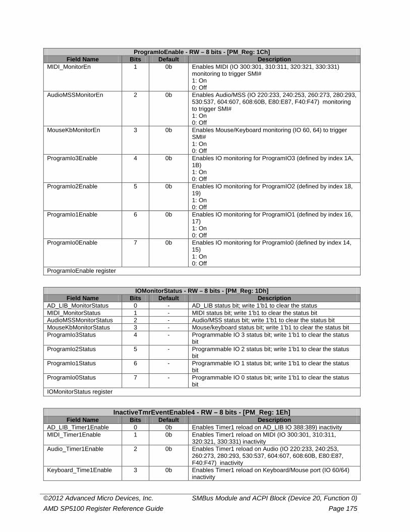
©2012 Advanced Micro Devices, Inc. SMBus Module and ACPI Block (Device 20, Function 0) AMD SP5100 Register Reference Guide Page 175
ProgramIoEnable - RW – 8 bits - [PM_Reg: 1Ch] Field Name Bits Default Description
MIDI_MonitorEn 1 0b Enables MIDI (IO 300:301, 310:311, 320:321, 330:331) monitoring to trigger SMI# 1: On 0: Off
AudioMSSMonitorEn 2 0b Enables Audio/MSS (IO 220:233, 240:253, 260:273, 280:293, 530:537, 604:607, 608:60B, E80:E87, F40:F47) monitoring to trigger SMI# 1: On 0: Off
MouseKbMonitorEn 3 0b Enables Mouse/Keyboard monitoring (IO 60, 64) to trigger SMI# 1: On 0: Off
ProgramIo3Enable 4 0b Enables IO monitoring for ProgramIO3 (defined by index 1A, 1B) 1: On 0: Off
ProgramIo2Enable 5 0b Enables IO monitoring for ProgramIO2 (defined by index 18, 19) 1: On 0: Off
ProgramIo1Enable 6 0b Enables IO monitoring for ProgramIO1 (defined by index 16, 17) 1: On 0: Off
ProgramIo0Enable 7 0b Enables IO monitoring for ProgramIo0 (defined by index 14, 15) 1: On 0: Off
ProgramIoEnable register
IOMonitorStatus - RW – 8 bits - [PM_Reg: 1Dh] Field Name Bits Default Description
AD_LIB_MonitorStatus 0 - AD_LIB status bit; write 1’b1 to clear the status MIDI_MonitorStatus 1 - MIDI status bit; write 1’b1 to clear the status bit AudioMSSMonitorStatus 2 - Audio/MSS status bit; write 1’b1 to clear the status bit MouseKbMonitorStatus 3 - Mouse/keyboard status bit; write 1’b1 to clear the status bit ProgramIo3Status 4 - Programmable IO 3 status bit; write 1’b1 to clear the status
bit ProgramIo2Status 5 - Programmable IO 2 status bit; write 1’b1 to clear the status
bit ProgramIo1Status 6 - Programmable IO 1 status bit; write 1’b1 to clear the status
bit ProgramIo0Status
7 - Programmable IO 0 status bit; write 1’b1 to clear the status bit
IOMonitorStatus register
InactiveTmrEventEnable4 - RW – 8 bits - [PM_Reg: 1Eh] Field Name Bits Default Description
AD_LIB_Timer1Enable 0 0b Enables Timer1 reload on AD_LIB IO 388:389) inactivity MIDI_Timer1Enable 1 0b Enables Timer1 reload on MIDI (IO 300:301, 310:311,
320:321, 330:331) inactivity Audio_Timer1Enable 2 0b Enables Timer1 reload on Audio (IO 220:233, 240:253,
260:273, 280:293, 530:537, 604:607, 608:60B, E80:E87, F40:F47) inactivity
Keyboard_Time1Enable 3 0b Enables Timer1 reload on Keyboard/Mouse port (IO 60/64) inactivity
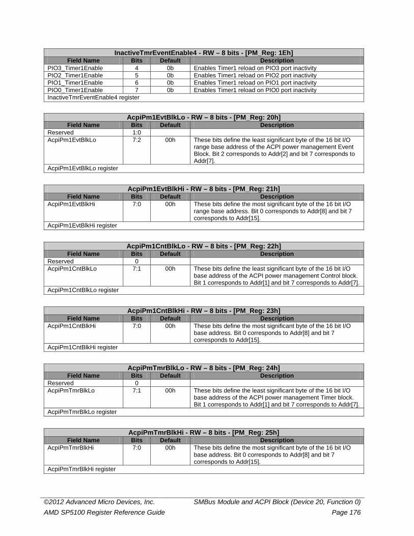
©2012 Advanced Micro Devices, Inc. SMBus Module and ACPI Block (Device 20, Function 0) AMD SP5100 Register Reference Guide Page 176
InactiveTmrEventEnable4 - RW – 8 bits - [PM_Reg: 1Eh] Field Name Bits Default Description
PIO3_Timer1Enable 4 0b Enables Timer1 reload on PIO3 port inactivity PIO2_Timer1Enable 5 0b Enables Timer1 reload on PIO2 port inactivity PIO1_Timer1Enable 6 0b Enables Timer1 reload on PIO1 port inactivity PIO0_Timer1Enable 7 0b Enables Timer1 reload on PIO0 port inactivity InactiveTmrEventEnable4 register
AcpiPm1EvtBlkLo - RW – 8 bits - [PM_Reg: 20h] Field Name Bits Default Description
Reserved 1:0 AcpiPm1EvtBlkLo 7:2 00h These bits define the least significant byte of the 16 bit I/O
range base address of the ACPI power management Event Block. Bit 2 corresponds to Addr[2] and bit 7 corresponds to Addr[7].
AcpiPm1EvtBlkLo register
AcpiPm1EvtBlkHi - RW – 8 bits - [PM_Reg: 21h] Field Name Bits Default Description
AcpiPm1EvtBlkHi 7:0 00h These bits define the most significant byte of the 16 bit I/O range base address. Bit 0 corresponds to Addr[8] and bit 7 corresponds to Addr[15].
AcpiPm1EvtBlkHi register
AcpiPm1CntBlkLo - RW – 8 bits - [PM_Reg: 22h] Field Name Bits Default Description
Reserved 0 AcpiPm1CntBlkLo 7:1 00h These bits define the least significant byte of the 16 bit I/O
base address of the ACPI power management Control block. Bit 1 corresponds to Addr[1] and bit 7 corresponds to Addr[7].
AcpiPm1CntBlkLo register
AcpiPm1CntBlkHi - RW – 8 bits - [PM_Reg: 23h] Field Name Bits Default Description
AcpiPm1CntBlkHi 7:0 00h These bits define the most significant byte of the 16 bit I/O base address. Bit 0 corresponds to Addr[8] and bit 7 corresponds to Addr[15].
AcpiPm1CntBlkHi register
AcpiPmTmrBlkLo - RW – 8 bits - [PM_Reg: 24h] Field Name Bits Default Description
Reserved 0 AcpiPmTmrBlkLo 7:1 00h These bits define the least significant byte of the 16 bit I/O
base address of the ACPI power management Timer block. Bit 1 corresponds to Addr[1] and bit 7 corresponds to Addr[7].
AcpiPmTmrBlkLo register
AcpiPmTmrBlkHi - RW – 8 bits - [PM_Reg: 25h] Field Name Bits Default Description
AcpiPmTmrBlkHi 7:0 00h These bits define the most significant byte of the 16 bit I/O base address. Bit 0 corresponds to Addr[8] and bit 7 corresponds to Addr[15].
AcpiPmTmrBlkHi register
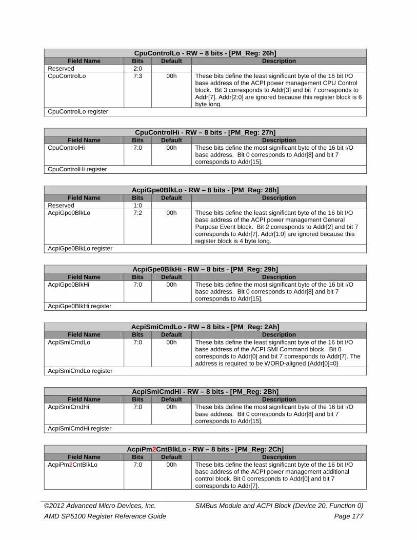
©2012 Advanced Micro Devices, Inc. SMBus Module and ACPI Block (Device 20, Function 0) AMD SP5100 Register Reference Guide Page 177
CpuControlLo - RW – 8 bits - [PM_Reg: 26h] Field Name Bits Default Description
Reserved 2:0 CpuControlLo 7:3 00h These bits define the least significant byte of the 16 bit I/O
base address of the ACPI power management CPU Control block. Bit 3 corresponds to Addr[3] and bit 7 corresponds to Addr[7]. Addr[2:0] are ignored because this register block is 6 byte long.
CpuControlLo register
CpuControlHi - RW – 8 bits - [PM_Reg: 27h] Field Name Bits Default Description
CpuControlHi 7:0 00h These bits define the most significant byte of the 16 bit I/O base address. Bit 0 corresponds to Addr[8] and bit 7 corresponds to Addr[15].
CpuControlHi register
AcpiGpe0BlkLo - RW – 8 bits - [PM_Reg: 28h] Field Name Bits Default Description
Reserved 1:0 AcpiGpe0BlkLo 7:2 00h These bits define the least significant byte of the 16 bit I/O
base address of the ACPI power management General Purpose Event block. Bit 2 corresponds to Addr[2] and bit 7 corresponds to Addr[7]. Addr[1:0] are ignored because this register block is 4 byte long.
AcpiGpe0BlkLo register
AcpiGpe0BlkHi - RW – 8 bits - [PM_Reg: 29h] Field Name Bits Default Description
AcpiGpe0BlkHi 7:0 00h These bits define the most significant byte of the 16 bit I/O base address. Bit 0 corresponds to Addr[8] and bit 7 corresponds to Addr[15].
AcpiGpe0BlkHi register
AcpiSmiCmdLo - RW – 8 bits - [PM_Reg: 2Ah] Field Name Bits Default Description
AcpiSmiCmdLo 7:0 00h These bits define the least significant byte of the 16 bit I/O base address of the ACPI SMI Command block. Bit 0 corresponds to Addr[0] and bit 7 corresponds to Addr[7]. The address is required to be WORD-aligned (Addr[0]=0)
AcpiSmiCmdLo register
AcpiSmiCmdHi - RW – 8 bits - [PM_Reg: 2Bh] Field Name Bits Default Description
AcpiSmiCmdHi 7:0 00h These bits define the most significant byte of the 16 bit I/O base address. Bit 0 corresponds to Addr[8] and bit 7 corresponds to Addr[15].
AcpiSmiCmdHi register
AcpiPm2CntBlkLo - RW – 8 bits - [PM_Reg: 2Ch] Field Name Bits Default Description
AcpiPm2CntBlkLo 7:0 00h These bits define the least significant byte of the 16 bit I/O base address of the ACPI power management additional control block. Bit 0 corresponds to Addr[0] and bit 7 corresponds to Addr[7].
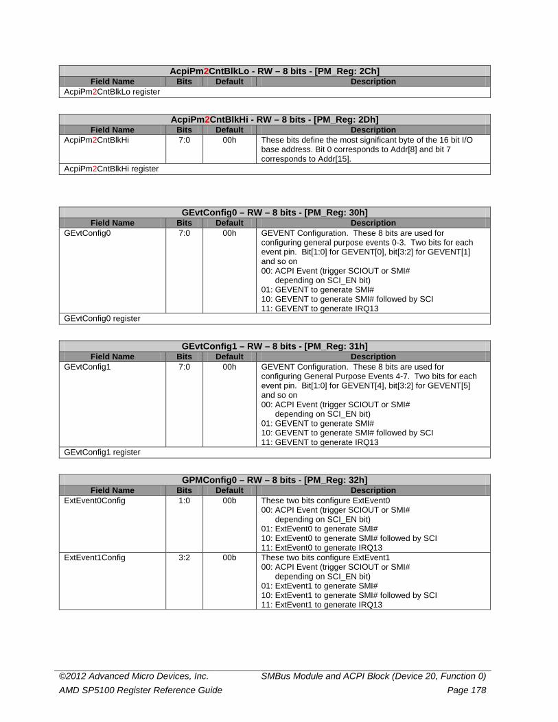
©2012 Advanced Micro Devices, Inc. SMBus Module and ACPI Block (Device 20, Function 0) AMD SP5100 Register Reference Guide Page 178
AcpiPm2CntBlkLo - RW – 8 bits - [PM_Reg: 2Ch] Field Name Bits Default Description
AcpiPm2CntBlkLo register
AcpiPm2CntBlkHi - RW – 8 bits - [PM_Reg: 2Dh] Field Name Bits Default Description
AcpiPm2CntBlkHi 7:0 00h These bits define the most significant byte of the 16 bit I/O base address. Bit 0 corresponds to Addr[8] and bit 7 corresponds to Addr[15].
AcpiPm2CntBlkHi register
GEvtConfig0 – RW – 8 bits - [PM_Reg: 30h] Field Name Bits Default Description
GEvtConfig0 7:0 00h GEVENT Configuration. These 8 bits are used for configuring general purpose events 0-3. Two bits for each event pin. Bit[1:0] for GEVENT[0], bit[3:2] for GEVENT[1] and so on 00: ACPI Event (trigger SCIOUT or SMI# depending on SCI_EN bit) 01: GEVENT to generate SMI# 10: GEVENT to generate SMI# followed by SCI 11: GEVENT to generate IRQ13
GEvtConfig0 register
GEvtConfig1 – RW – 8 bits - [PM_Reg: 31h] Field Name Bits Default Description
GEvtConfig1 7:0 00h GEVENT Configuration. These 8 bits are used for configuring General Purpose Events 4-7. Two bits for each event pin. Bit[1:0] for GEVENT[4], bit[3:2] for GEVENT[5] and so on 00: ACPI Event (trigger SCIOUT or SMI# depending on SCI_EN bit) 01: GEVENT to generate SMI# 10: GEVENT to generate SMI# followed by SCI 11: GEVENT to generate IRQ13
GEvtConfig1 register
GPMConfig0 – RW – 8 bits - [PM_Reg: 32h] Field Name Bits Default Description
ExtEvent0Config 1:0 00b These two bits configure ExtEvent0 00: ACPI Event (trigger SCIOUT or SMI# depending on SCI_EN bit) 01: ExtEvent0 to generate SMI# 10: ExtEvent0 to generate SMI# followed by SCI 11: ExtEvent0 to generate IRQ13
ExtEvent1Config 3:2 00b These two bits configure ExtEvent1 00: ACPI Event (trigger SCIOUT or SMI# depending on SCI_EN bit) 01: ExtEvent1 to generate SMI# 10: ExtEvent1 to generate SMI# followed by SCI 11: ExtEvent1 to generate IRQ13
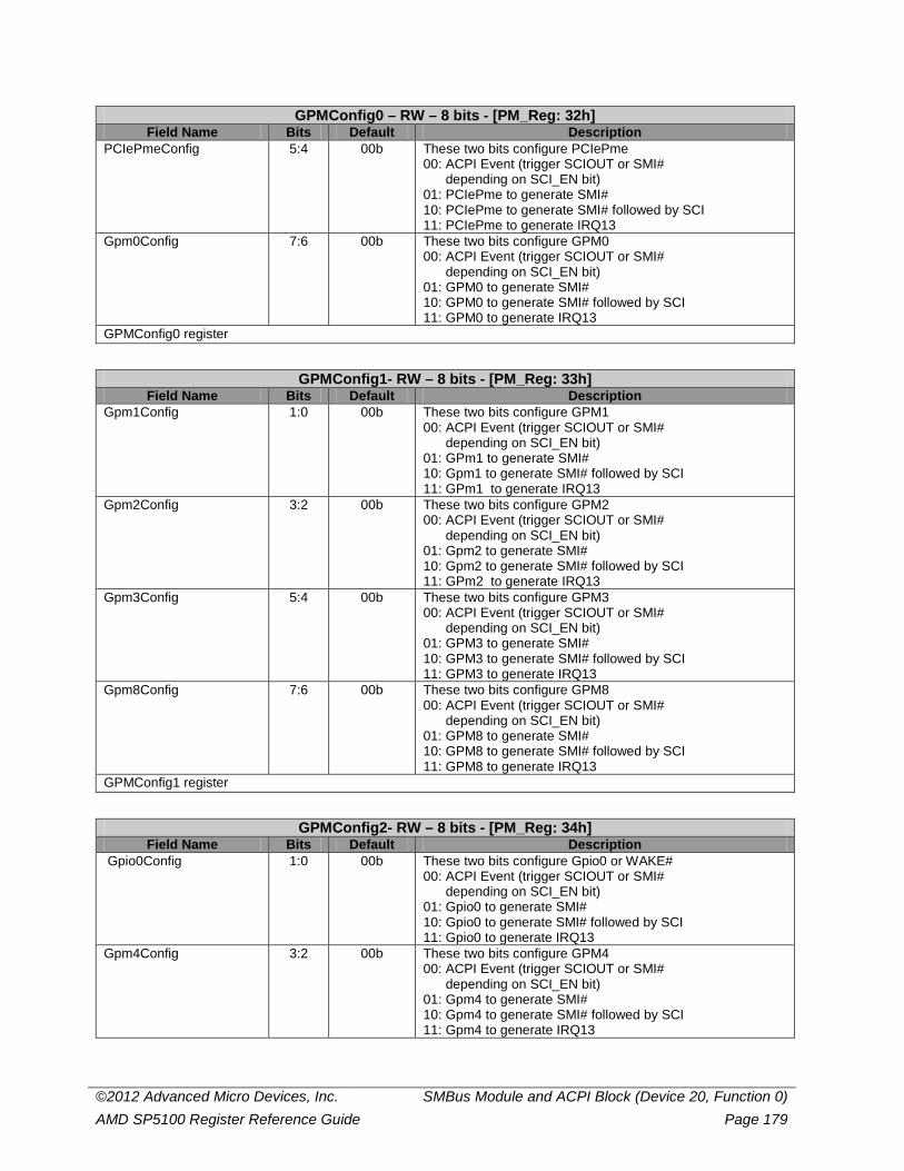
©2012 Advanced Micro Devices, Inc. SMBus Module and ACPI Block (Device 20, Function 0) AMD SP5100 Register Reference Guide Page 179
GPMConfig0 – RW – 8 bits - [PM_Reg: 32h] Field Name Bits Default Description
PCIePmeConfig 5:4 00b These two bits configure PCIePme 00: ACPI Event (trigger SCIOUT or SMI# depending on SCI_EN bit) 01: PCIePme to generate SMI# 10: PCIePme to generate SMI# followed by SCI 11: PCIePme to generate IRQ13
Gpm0Config 7:6 00b These two bits configure GPM0 00: ACPI Event (trigger SCIOUT or SMI# depending on SCI_EN bit) 01: GPM0 to generate SMI# 10: GPM0 to generate SMI# followed by SCI 11: GPM0 to generate IRQ13
GPMConfig0 register
GPMConfig1- RW – 8 bits - [PM_Reg: 33h] Field Name Bits Default Description
Gpm1Config 1:0 00b These two bits configure GPM1 00: ACPI Event (trigger SCIOUT or SMI# depending on SCI_EN bit) 01: GPm1 to generate SMI# 10: Gpm1 to generate SMI# followed by SCI 11: GPm1 to generate IRQ13
Gpm2Config 3:2 00b These two bits configure GPM2 00: ACPI Event (trigger SCIOUT or SMI# depending on SCI_EN bit) 01: Gpm2 to generate SMI# 10: Gpm2 to generate SMI# followed by SCI 11: GPm2 to generate IRQ13
Gpm3Config 5:4 00b These two bits configure GPM3 00: ACPI Event (trigger SCIOUT or SMI# depending on SCI_EN bit) 01: GPM3 to generate SMI# 10: GPM3 to generate SMI# followed by SCI 11: GPM3 to generate IRQ13
Gpm8Config 7:6 00b These two bits configure GPM8 00: ACPI Event (trigger SCIOUT or SMI# depending on SCI_EN bit) 01: GPM8 to generate SMI# 10: GPM8 to generate SMI# followed by SCI 11: GPM8 to generate IRQ13
GPMConfig1 register
GPMConfig2- RW – 8 bits - [PM_Reg: 34h] Field Name Bits Default Description
Gpio0Config 1:0 00b These two bits configure Gpio0 or WAKE# 00: ACPI Event (trigger SCIOUT or SMI# depending on SCI_EN bit) 01: Gpio0 to generate SMI# 10: Gpio0 to generate SMI# followed by SCI 11: Gpio0 to generate IRQ13
Gpm4Config 3:2 00b These two bits configure GPM4 00: ACPI Event (trigger SCIOUT or SMI# depending on SCI_EN bit) 01: Gpm4 to generate SMI# 10: Gpm4 to generate SMI# followed by SCI 11: Gpm4 to generate IRQ13
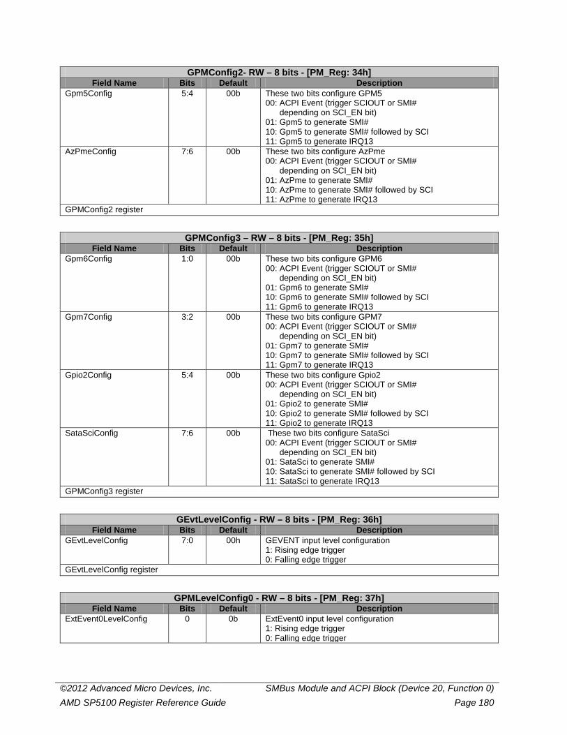
©2012 Advanced Micro Devices, Inc. SMBus Module and ACPI Block (Device 20, Function 0) AMD SP5100 Register Reference Guide Page 180
GPMConfig2- RW – 8 bits - [PM_Reg: 34h] Field Name Bits Default Description
Gpm5Config 5:4 00b These two bits configure GPM5 00: ACPI Event (trigger SCIOUT or SMI# depending on SCI_EN bit) 01: Gpm5 to generate SMI# 10: Gpm5 to generate SMI# followed by SCI 11: Gpm5 to generate IRQ13
AzPmeConfig 7:6 00b These two bits configure AzPme 00: ACPI Event (trigger SCIOUT or SMI# depending on SCI_EN bit) 01: AzPme to generate SMI# 10: AzPme to generate SMI# followed by SCI 11: AzPme to generate IRQ13
GPMConfig2 register
GPMConfig3 – RW – 8 bits - [PM_Reg: 35h] Field Name Bits Default Description
Gpm6Config 1:0 00b These two bits configure GPM6 00: ACPI Event (trigger SCIOUT or SMI# depending on SCI_EN bit) 01: Gpm6 to generate SMI# 10: Gpm6 to generate SMI# followed by SCI 11: Gpm6 to generate IRQ13
Gpm7Config 3:2 00b These two bits configure GPM7 00: ACPI Event (trigger SCIOUT or SMI# depending on SCI_EN bit) 01: Gpm7 to generate SMI# 10: Gpm7 to generate SMI# followed by SCI 11: Gpm7 to generate IRQ13
Gpio2Config 5:4 00b These two bits configure Gpio2 00: ACPI Event (trigger SCIOUT or SMI# depending on SCI_EN bit) 01: Gpio2 to generate SMI# 10: Gpio2 to generate SMI# followed by SCI 11: Gpio2 to generate IRQ13
SataSciConfig
7:6 00b These two bits configure SataSci 00: ACPI Event (trigger SCIOUT or SMI# depending on SCI_EN bit) 01: SataSci to generate SMI# 10: SataSci to generate SMI# followed by SCI 11: SataSci to generate IRQ13
GPMConfig3 register
GEvtLevelConfig - RW – 8 bits - [PM_Reg: 36h] Field Name Bits Default Description
GEvtLevelConfig 7:0 00h GEVENT input level configuration 1: Rising edge trigger 0: Falling edge trigger
GEvtLevelConfig register
GPMLevelConfig0 - RW – 8 bits - [PM_Reg: 37h] Field Name Bits Default Description
ExtEvent0LevelConfig 0 0b ExtEvent0 input level configuration 1: Rising edge trigger 0: Falling edge trigger
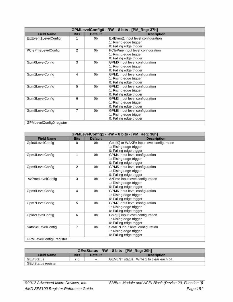
©2012 Advanced Micro Devices, Inc. SMBus Module and ACPI Block (Device 20, Function 0) AMD SP5100 Register Reference Guide Page 181
GPMLevelConfig0 - RW – 8 bits - [PM_Reg: 37h] Field Name Bits Default Description
ExtEvent1LevelConfig 1 0b ExtEvent1 input level configuration 1: Rising edge trigger 0: Falling edge trigger
PCIePmeLevelConfig 2 0b PCIePme input level configuration 1: Rising edge trigger 0: Falling edge trigger
Gpm0LevelConfig 3 0b GPM0 input level configuration 1: Rising edge trigger 0: Falling edge trigger
Gpm1LevelConfig 4 0b GPM1 input level configuration 1: Rising edge trigger 0: Falling edge trigger
Gpm2LevelConfig 5 0b GPM2 input level configuration 1: Rising edge trigger 0: Falling edge trigger
Gpm3LevelConfig 6 0b GPM3 input level configuration 1: Rising edge trigger 0: Falling edge trigger
Gpm8LevelConfig 7 0b GPM8 input level configuration 1: Rising edge trigger 0: Falling edge trigger
GPMLevelConfig0 register
GPMLevelConfig1 - RW – 8 bits - [PM_Reg: 38h] Field Name Bits Default Description
Gpio0LevelConfig 0 0b Gpio[0] or WAKE# input level configuration 1: Rising edge trigger 0: Falling edge trigger
Gpm4LevelConfig 1 0b GPM4 input level configuration 1: Rising edge trigger 0: Falling edge trigger
Gpm5LevelConfig 2 0b GPM5 input level configuration 1: Rising edge trigger 0: Falling edge trigger
AzPmeLevelConfig 3 0b AzPme input level configuration 1: Rising edge trigger 0: Falling edge trigger
Gpm6LevelConfig 4 0b GPM6 input level configuration 1: Rising edge trigger 0: Falling edge trigger
Gpm7LevelConfig 5 0b GPM7 input level configuration 1: Rising edge trigger 0: Falling edge trigger
Gpio2LevelConfig 6 0b Gpio[2] input level configuration 1: Rising edge trigger 0: Falling edge trigger
SataSciLevelConfig 7 0b SataSci input level configuration 1: Rising edge trigger 0: Falling edge trigger
GPMLevelConfig1 register
GEvtStatus - RW – 8 bits - [PM_Reg: 39h] Field Name Bits Default Description
GEvtStatus 7:0 -- GEVENT status. Write 1 to clear each bit GEvtStatus register
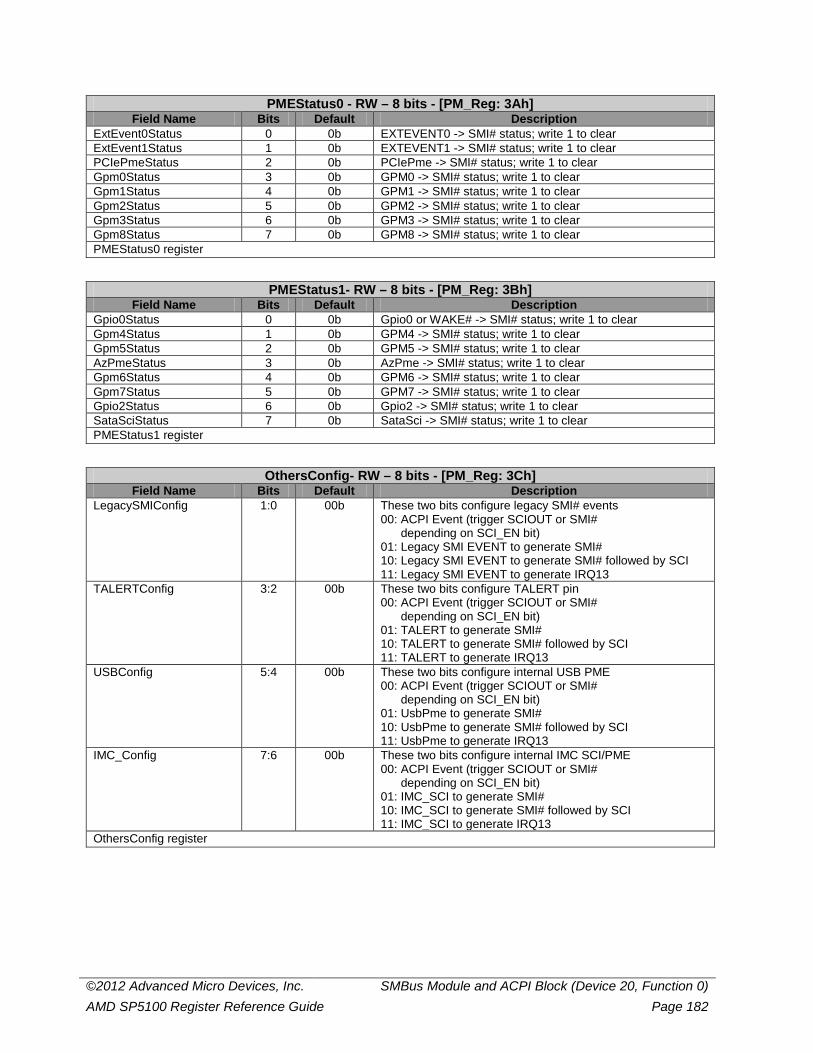
©2012 Advanced Micro Devices, Inc. SMBus Module and ACPI Block (Device 20, Function 0) AMD SP5100 Register Reference Guide Page 182
PMEStatus0 - RW – 8 bits - [PM_Reg: 3Ah] Field Name Bits Default Description
ExtEvent0Status 0 0b EXTEVENT0 -> SMI# status; write 1 to clear ExtEvent1Status 1 0b EXTEVENT1 -> SMI# status; write 1 to clear PCIePmeStatus 2 0b PCIePme -> SMI# status; write 1 to clear Gpm0Status 3 0b GPM0 -> SMI# status; write 1 to clear Gpm1Status 4 0b GPM1 -> SMI# status; write 1 to clear Gpm2Status 5 0b GPM2 -> SMI# status; write 1 to clear Gpm3Status 6 0b GPM3 -> SMI# status; write 1 to clear Gpm8Status 7 0b GPM8 -> SMI# status; write 1 to clear PMEStatus0 register
PMEStatus1- RW – 8 bits - [PM_Reg: 3Bh] Field Name Bits Default Description
Gpio0Status 0 0b Gpio0 or WAKE# -> SMI# status; write 1 to clear Gpm4Status 1 0b GPM4 -> SMI# status; write 1 to clear Gpm5Status 2 0b GPM5 -> SMI# status; write 1 to clear AzPmeStatus 3 0b AzPme -> SMI# status; write 1 to clear Gpm6Status 4 0b GPM6 -> SMI# status; write 1 to clear Gpm7Status 5 0b GPM7 -> SMI# status; write 1 to clear Gpio2Status 6 0b Gpio2 -> SMI# status; write 1 to clear SataSciStatus 7 0b SataSci -> SMI# status; write 1 to clear PMEStatus1 register
OthersConfig- RW – 8 bits - [PM_Reg: 3Ch] Field Name Bits Default Description
LegacySMIConfig 1:0 00b These two bits configure legacy SMI# events 00: ACPI Event (trigger SCIOUT or SMI# depending on SCI_EN bit) 01: Legacy SMI EVENT to generate SMI# 10: Legacy SMI EVENT to generate SMI# followed by SCI 11: Legacy SMI EVENT to generate IRQ13
TALERTConfig 3:2 00b These two bits configure TALERT pin 00: ACPI Event (trigger SCIOUT or SMI# depending on SCI_EN bit) 01: TALERT to generate SMI# 10: TALERT to generate SMI# followed by SCI 11: TALERT to generate IRQ13
USBConfig 5:4 00b These two bits configure internal USB PME 00: ACPI Event (trigger SCIOUT or SMI# depending on SCI_EN bit) 01: UsbPme to generate SMI# 10: UsbPme to generate SMI# followed by SCI 11: UsbPme to generate IRQ13
IMC_Config 7:6 00b These two bits configure internal IMC SCI/PME 00: ACPI Event (trigger SCIOUT or SMI# depending on SCI_EN bit) 01: IMC_SCI to generate SMI# 10: IMC_SCI to generate SMI# followed by SCI 11: IMC_SCI to generate IRQ13
OthersConfig register
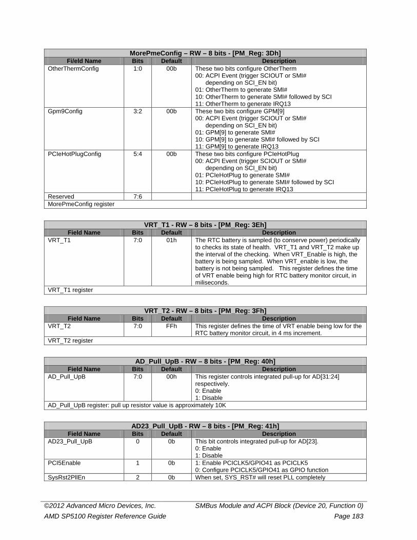
©2012 Advanced Micro Devices, Inc. SMBus Module and ACPI Block (Device 20, Function 0) AMD SP5100 Register Reference Guide Page 183
MorePmeConfig – RW – 8 bits - [PM_Reg: 3Dh] Fi/eld Name Bits Default Description
OtherThermConfig 1:0 00b These two bits configure OtherTherm 00: ACPI Event (trigger SCIOUT or SMI# depending on SCI_EN bit) 01: OtherTherm to generate SMI# 10: OtherTherm to generate SMI# followed by SCI 11: OtherTherm to generate IRQ13
Gpm9Config 3:2 00b These two bits configure GPM[9] 00: ACPI Event (trigger SCIOUT or SMI# depending on SCI_EN bit) 01: GPM[9] to generate SMI# 10: GPM[9] to generate SMI# followed by SCI 11: GPM[9] to generate IRQ13
PCIeHotPlugConfig 5:4 00b These two bits configure PCIeHotPlug 00: ACPI Event (trigger SCIOUT or SMI# depending on SCI_EN bit) 01: PCIeHotPlug to generate SMI# 10: PCIeHotPlug to generate SMI# followed by SCI 11: PCIeHotPlug to generate IRQ13
Reserved 7:6 MorePmeConfig register
VRT_T1 - RW – 8 bits - [PM_Reg: 3Eh] Field Name Bits Default Description
VRT_T1 7:0 01h The RTC battery is sampled (to conserve power) periodically to checks its state of health. VRT_T1 and VRT_T2 make up the interval of the checking. When VRT_Enable is high, the battery is being sampled. When VRT_enable is low, the battery is not being sampled. This register defines the time of VRT enable being high for RTC battery monitor circuit, in miliseconds.
VRT_T1 register
VRT_T2 - RW – 8 bits - [PM_Reg: 3Fh] Field Name Bits Default Description
VRT_T2 7:0 FFh This register defines the time of VRT enable being low for the RTC battery monitor circuit, in 4 ms increment.
VRT_T2 register
AD_Pull_UpB - RW – 8 bits - [PM_Reg: 40h] Field Name Bits Default Description
AD_Pull_UpB 7:0 00h This register controls integrated pull-up for AD[31:24] respectively. 0: Enable 1: Disable
AD_Pull_UpB register: pull up resistor value is approximately 10K
AD23_Pull_UpB - RW – 8 bits - [PM_Reg: 41h] Field Name Bits Default Description
AD23_Pull_UpB 0 0b This bit controls integrated pull-up for AD[23]. 0: Enable 1: Disable
PCI5Enable 1 0b 1: Enable PCICLK5/GPIO41 as PCICLK5 0: Configure PCICLK5/GPIO41 as GPIO function
SysRst2PllEn 2 0b When set, SYS_RST# will reset PLL completely
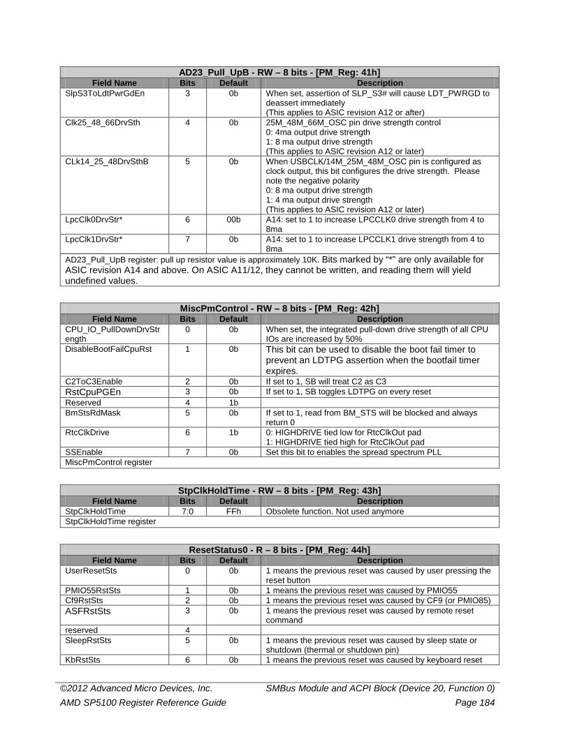
©2012 Advanced Micro Devices, Inc. SMBus Module and ACPI Block (Device 20, Function 0) AMD SP5100 Register Reference Guide Page 184
AD23_Pull_UpB - RW – 8 bits - [PM_Reg: 41h] Field Name Bits Default Description
SlpS3ToLdtPwrGdEn 3 0b When set, assertion of SLP_S3# will cause LDT_PWRGD to deassert immediately (This applies to ASIC revision A12 or after)
Clk25_48_66DrvSth 4 0b 25M_48M_66M_OSC pin drive strength control 0: 4ma output drive strength 1: 8 ma output drive strength (This applies to ASIC revision A12 or later)
CLk14_25_48DrvSthB 5 0b When USBCLK/14M_25M_48M_OSC pin is configured as clock output, this bit configures the drive strength. Please note the negative polarity 0: 8 ma output drive strength 1: 4 ma output drive strength (This applies to ASIC revision A12 or later)
LpcClk0DrvStr* 6 00b A14: set to 1 to increase LPCCLK0 drive strength from 4 to 8ma
LpcClk1DrvStr* 7 0b A14: set to 1 to increase LPCCLK1 drive strength from 4 to 8ma
AD23_Pull_UpB register: pull up resistor value is approximately 10K. Bits marked by “*” are only available for ASIC revision A14 and above. On ASIC A11/12, they cannot be written, and reading them will yield undefined values.
MiscPmControl - RW – 8 bits - [PM_Reg: 42h] Field Name Bits Default Description
CPU_IO_PullDownDrvStrength
0 0b When set, the integrated pull-down drive strength of all CPU IOs are increased by 50%
DisableBootFailCpuRst 1 0b This bit can be used to disable the boot fail timer to prevent an LDTPG assertion when the bootfail timer expires.
C2ToC3Enable 2 0b If set to 1, SB will treat C2 as C3 RstCpuPGEn 3 0b If set to 1, SB toggles LDTPG on every reset Reserved 4 1b BmStsRdMask 5 0b If set to 1, read from BM_STS will be blocked and always
return 0 RtcClkDrive 6 1b 0: HIGHDRIVE tied low for RtcClkOut pad
1: HIGHDRIVE tied high for RtcClkOut pad SSEnable 7 0b Set this bit to enables the spread spectrum PLL MiscPmControl register
StpClkHoldTime - RW – 8 bits - [PM_Reg: 43h] Field Name Bits Default Description
StpClkHoldTime 7:0 FFh Obsolete function. Not used anymore StpClkHoldTime register
ResetStatus0 - R – 8 bits - [PM_Reg: 44h] Field Name Bits Default Description
UserResetSts 0 0b 1 means the previous reset was caused by user pressing the reset button
PMIO55RstSts 1 0b 1 means the previous reset was caused by PMIO55 Cf9RstSts 2 0b 1 means the previous reset was caused by CF9 (or PMIO85) ASFRstSts 3 0b 1 means the previous reset was caused by remote reset
command reserved 4 SleepRstSts 5 0b 1 means the previous reset was caused by sleep state or
shutdown (thermal or shutdown pin) KbRstSts 6 0b 1 means the previous reset was caused by keyboard reset
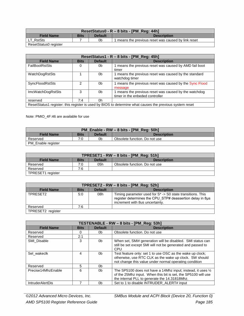
©2012 Advanced Micro Devices, Inc. SMBus Module and ACPI Block (Device 20, Function 0) AMD SP5100 Register Reference Guide Page 185
ResetStatus0 - R – 8 bits - [PM_Reg: 44h] Field Name Bits Default Description
LT_RstSts 7 0b 1 means the previous reset was caused by link reset ResetStatus0 register
ResetStatus1 - R – 8 bits - [PM_Reg: 45h] Field Name Bits Default Description
FailBootRstSts 0 0b 1 means the previous reset was caused by AMD fail boot timer
WatchDogRstSts 1 0b 1 means the previous reset was caused by the standard watchdog timer
SyncFloodRstSts 2 0b 1 means the previous reset was caused by the Sync Flood message
ImcWatchDogRstSts 3 0b 1 means the previous reset was caused by the watchdog timer in the enbeded controller
reserved 7:4 0h ResetStatus1 register: this register is used by BIOS to determine what causes the previous system reset
Note: PMIO_4F:46 are available for use
PM_Enable - RW – 8 bits - [PM_Reg: 50h] Field Name Bits Default Description
Reserved 7:0 0b Obsolete function. Do not use PM_Enable register
TPRESET1 - RW – 8 bits - [PM_Reg: 51h] Field Name Bits Default Description
Reserved 7:0 05h Obsolete function. Do not use Reserved 7:6 TPRESET1 register
TPRESET2 - RW – 8 bits - [PM_Reg: 52h] Field Name Bits Default Description
TPRESET2 5:0 08h Timing parameter used for S* -> S0 state transitions. This register determines the CPU_STP# deassertion delay in 8μs increment with 8us uncertainty.
Reserved 7:6 TPRESET2 register
TESTENABLE - RW – 8 bits - [PM_Reg: 53h] Field Name Bits Default Description
Reserved 0 0b Obsolete function. Do not use Reserved 2:1 SMI_Disable 3 0b When set, SMI# generation will be disabled. SMI status can
still be set except SMI will not be generated and passed to CPU
Sel_wakeclk 4 0b Test feature only: set 1 to use OSC as the wake up clock; otherwise, use RTC CLK as the wake up clock. SW should not change this value under normal operating condition
Reserved 5 0b Precise14MhzEnable 6 0b The SP5100 does not have a 14Mhz input; instead, it uses ½
of the 25Mhz input. When this bit is set, the SP5100 will use the internal PLL to generate the 14.31818Mhz.
IntruderAlertDis 7 0b Set to 1 to disable INTRUDER_ALERT# input
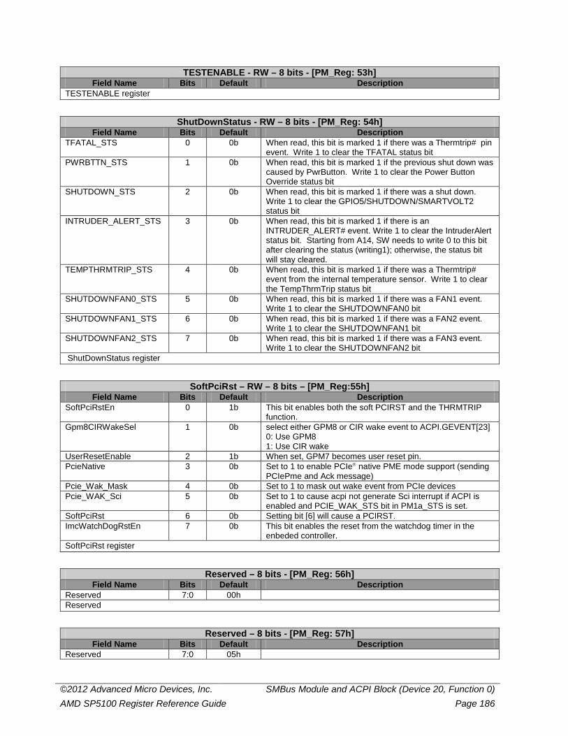
©2012 Advanced Micro Devices, Inc. SMBus Module and ACPI Block (Device 20, Function 0) AMD SP5100 Register Reference Guide Page 186
TESTENABLE - RW – 8 bits - [PM_Reg: 53h] Field Name Bits Default Description
TESTENABLE register
ShutDownStatus - RW – 8 bits - [PM_Reg: 54h] Field Name Bits Default Description
TFATAL_STS 0 0b When read, this bit is marked 1 if there was a Thermtrip# pin event. Write 1 to clear the TFATAL status bit
PWRBTTN_STS 1 0b When read, this bit is marked 1 if the previous shut down was caused by PwrButton. Write 1 to clear the Power Button Override status bit
SHUTDOWN_STS 2 0b When read, this bit is marked 1 if there was a shut down. Write 1 to clear the GPIO5/SHUTDOWN/SMARTVOLT2 status bit
INTRUDER_ALERT_STS 3 0b When read, this bit is marked 1 if there is an INTRUDER_ALERT# event. Write 1 to clear the IntruderAlert status bit. Starting from A14, SW needs to write 0 to this bit after clearing the status (writing1); otherwise, the status bit will stay cleared.
TEMPTHRMTRIP_STS 4 0b When read, this bit is marked 1 if there was a Thermtrip# event from the internal temperature sensor. Write 1 to clear the TempThrmTrip status bit
SHUTDOWNFAN0_STS 5 0b When read, this bit is marked 1 if there was a FAN1 event. Write 1 to clear the SHUTDOWNFAN0 bit
SHUTDOWNFAN1_STS 6 0b When read, this bit is marked 1 if there was a FAN2 event. Write 1 to clear the SHUTDOWNFAN1 bit
SHUTDOWNFAN2_STS 7 0b When read, this bit is marked 1 if there was a FAN3 event. Write 1 to clear the SHUTDOWNFAN2 bit
ShutDownStatus register
SoftPciRst – RW – 8 bits – [PM_Reg:55h] Field Name Bits Default Description
SoftPciRstEn 0 1b This bit enables both the soft PCIRST and the THRMTRIP function.
Gpm8CIRWakeSel 1 0b select either GPM8 or CIR wake event to ACPI.GEVENT[23] 0: Use GPM8 1: Use CIR wake
UserResetEnable 2 1b When set, GPM7 becomes user reset pin. PcieNative 3 0b Set to 1 to enable PCIe native PME mode support (sending
PCIePme and Ack message) Pcie_Wak_Mask 4 0b Set to 1 to mask out wake event from PCIe devices Pcie_WAK_Sci 5 0b Set to 1 to cause acpi not generate Sci interrupt if ACPI is
enabled and PCIE_WAK_STS bit in PM1a_STS is set. SoftPciRst 6 0b Setting bit [6] will cause a PCIRST. ImcWatchDogRstEn 7 0b This bit enables the reset from the watchdog timer in the
enbeded controller. SoftPciRst register
Reserved – 8 bits - [PM_Reg: 56h] Field Name Bits Default Description
Reserved 7:0 00h Reserved
Reserved – 8 bits - [PM_Reg: 57h] Field Name Bits Default Description
Reserved 7:0 05h
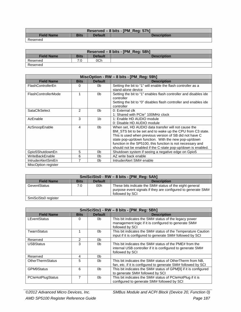
©2012 Advanced Micro Devices, Inc. SMBus Module and ACPI Block (Device 20, Function 0) AMD SP5100 Register Reference Guide Page 187
Reserved – 8 bits - [PM_Reg: 57h] Field Name Bits Default Description
Reserved
Reserved – 8 bits - [PM_Reg: 58h] Field Name Bits Default Description
Reserved 7:0 0Ch Reserved
MiscOption - RW – 8 bits - [PM_Reg: 59h] Field Name Bits Default Description
FlashControllerEn 0 0b Setting the bit to “1” will enable the flash controller as a stand-alone device
FlashControllerMode 1 0b Setting the bit to “1” enables flash controller and disables ide controller Setting the bit to “0” disables flash controller and enables ide controller
SataClkSelect 2 0b 0: External clk 1: Shared with PCIe 100MHz clock
AzEnable 3 1b 1: Enable HD AUDIO module 0: Disable HD AUDIO module
AzSnoopEnable 4 0b When set, HD AUDIO data transfer will not cause the BM_STS bit to be set and to wake up the CPU from C3 state. This is used when previous version of SB did not have C state pop-up/down function. With the new pop-up/down function in the SP5100, this function is not necessary and should not be enabled if the C-state pop-up/down is enabled.
Gpio5ShutdownEn 5 0b Shutdown system if seeing a negative edge on Gpio5 WriteBackEnable 6 0b AZ write back enable IntruderAlertSmiEn 7 0b IntruderAlert SMI# enable MiscOption register
SmiSciSts0 - RW – 8 bits - [PM_Reg: 5Ah] Field Name Bits Default Description
GeventStatus 7:0 00h These bits indicate the SMI# status of the eight general purpose event signals if they are configured to generate SMI# followed by SCI
SmiSciSts0 register
SmiSciSts1 - RW – 8 bits - [PM_Reg: 5Bh] Field Name Bits Default Description
LEventStatus 0 0b This bit indicates the SMI# status of the legacy power management logic if it is configured to generate SMI# followed by SCI
TwarnStatus 1 0b This bit indicates the SMI# status of the Temperature Caution input if it is configured to generate SMI# followed by SCI
Reserved 2 0b USBStatus 3 0b This bit indicates the SMI# status of the PME# from the
internal USB controller if it is configured to generate SMI# followed by SCI
Reserved 4 0b OtherThermStatus 5 0b This bit indicates the SMI# status of OtherTherm from NB,
fan, etc. if it is configured to generate SMI# followed by SCI GPM9Status 6 0b This bit indicates the SMI# status of GPM[9] if it is configured
to generate SMI# followed by SCI PCIeHotPlugStatus 7 0b This bit indicates the SMI# status of PCIeHotPlug if it is
configured to generate SMI# followed by SCI
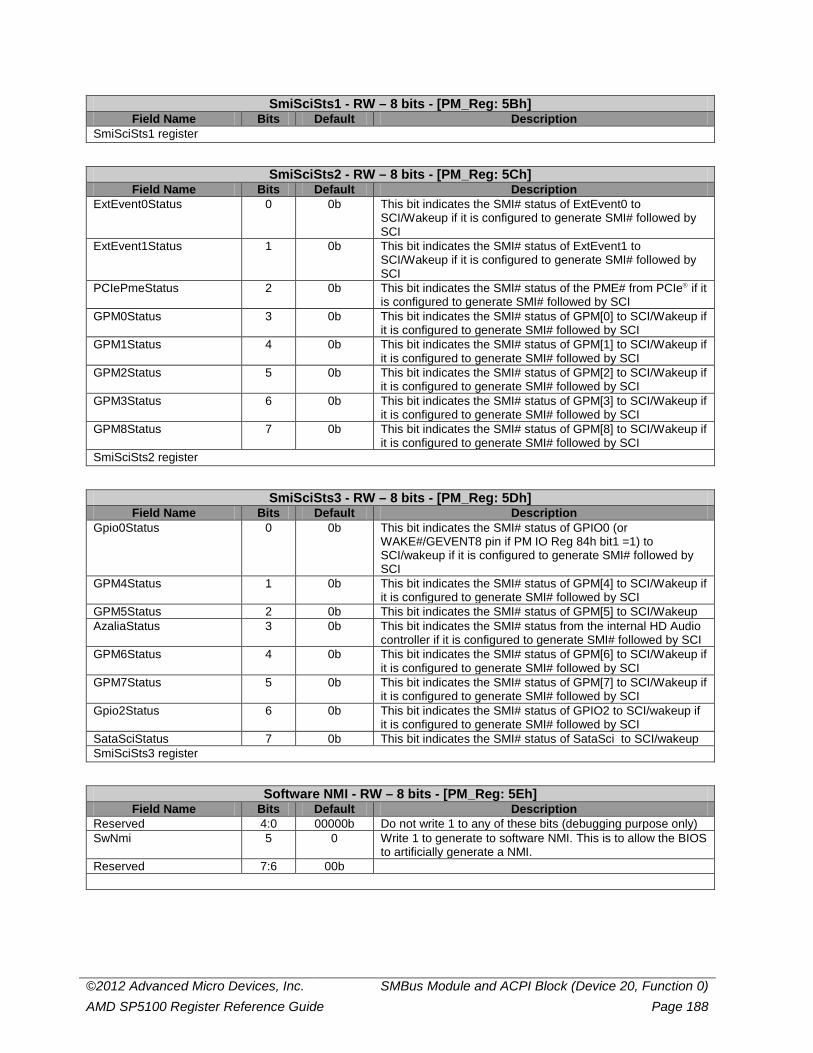
©2012 Advanced Micro Devices, Inc. SMBus Module and ACPI Block (Device 20, Function 0) AMD SP5100 Register Reference Guide Page 188
SmiSciSts1 - RW – 8 bits - [PM_Reg: 5Bh] Field Name Bits Default Description
SmiSciSts1 register
SmiSciSts2 - RW – 8 bits - [PM_Reg: 5Ch] Field Name Bits Default Description
ExtEvent0Status 0 0b This bit indicates the SMI# status of ExtEvent0 to SCI/Wakeup if it is configured to generate SMI# followed by SCI
ExtEvent1Status 1 0b This bit indicates the SMI# status of ExtEvent1 to SCI/Wakeup if it is configured to generate SMI# followed by SCI
PCIePmeStatus 2 0b This bit indicates the SMI# status of the PME# from PCIe if it is configured to generate SMI# followed by SCI
GPM0Status 3 0b This bit indicates the SMI# status of GPM[0] to SCI/Wakeup if it is configured to generate SMI# followed by SCI
GPM1Status 4 0b This bit indicates the SMI# status of GPM[1] to SCI/Wakeup if it is configured to generate SMI# followed by SCI
GPM2Status 5 0b This bit indicates the SMI# status of GPM[2] to SCI/Wakeup if it is configured to generate SMI# followed by SCI
GPM3Status 6 0b This bit indicates the SMI# status of GPM[3] to SCI/Wakeup if it is configured to generate SMI# followed by SCI
GPM8Status 7 0b This bit indicates the SMI# status of GPM[8] to SCI/Wakeup if it is configured to generate SMI# followed by SCI
SmiSciSts2 register
SmiSciSts3 - RW – 8 bits - [PM_Reg: 5Dh] Field Name Bits Default Description
Gpio0Status 0 0b This bit indicates the SMI# status of GPIO0 (or WAKE#/GEVENT8 pin if PM IO Reg 84h bit1 =1) to SCI/wakeup if it is configured to generate SMI# followed by SCI
GPM4Status 1 0b This bit indicates the SMI# status of GPM[4] to SCI/Wakeup if it is configured to generate SMI# followed by SCI
GPM5Status 2 0b This bit indicates the SMI# status of GPM[5] to SCI/Wakeup AzaliaStatus 3 0b This bit indicates the SMI# status from the internal HD Audio
controller if it is configured to generate SMI# followed by SCI GPM6Status 4 0b This bit indicates the SMI# status of GPM[6] to SCI/Wakeup if
it is configured to generate SMI# followed by SCI GPM7Status 5 0b This bit indicates the SMI# status of GPM[7] to SCI/Wakeup if
it is configured to generate SMI# followed by SCI Gpio2Status 6 0b This bit indicates the SMI# status of GPIO2 to SCI/wakeup if
it is configured to generate SMI# followed by SCI SataSciStatus 7 0b This bit indicates the SMI# status of SataSci to SCI/wakeup SmiSciSts3 register
Software NMI - RW – 8 bits - [PM_Reg: 5Eh] Field Name Bits Default Description
Reserved 4:0 00000b Do not write 1 to any of these bits (debugging purpose only) SwNmi 5 0 Write 1 to generate to software NMI. This is to allow the BIOS
to artificially generate a NMI. Reserved 7:6 00b
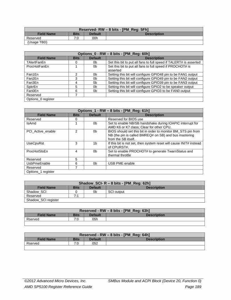
©2012 Advanced Micro Devices, Inc. SMBus Module and ACPI Block (Device 20, Function 0) AMD SP5100 Register Reference Guide Page 189
Reserved- RW – 8 bits - [PM_Reg: 5Fh] Field Name Bits Default Description
Reserved 7:0 00h (Usage TBD)
Options_0 - RW – 8 bits - [PM_Reg: 60h] Field Name Bits Default Description
TAlertFanEn 0 0b Set this bit to put all fans to full speed if TALERT# is asserted ProcHotFanEn 1 0b Set this bit to put all fans to full speed if PROCHOT# is
asserted Fan1En 2 0b Setting this bit will configure GPIO48 pin to be FAN1 output Fan2En 3 0b Setting this bit will configure GPIO49 pin to be FAN2 output Fan3En 4 0b Setting this bit will configure GPIO39 pin to be FAN3 output SpkrEn 5 0b Setting this bit will configure GPIO2 to be speaker output Fan0En 6 0b Setting this bit will configure GPIO3 to be FAN0 output Reserved 7 Options_0 register
Options_1 - RW – 8 bits - [PM_Reg: 61h] Field Name Bits Default Description
Reserved 0 Reserved for BIOS use IsAmd 1 0b Set to enable NB/SB handshake during IOAPIC interrupt for
AMD K6 or K7 class; Clear for other CPU. PCI_Active_enable 2 0b BIOS should set this bit in order to monitor BM_STS pin from
NB (the pin is called BMREQ# on SB) and bus mastering from the SB itself.
UseCpuRst 3 1b If this bit is not set, then system reset will cause INIT# instead of CPURST#.
ProcHotStsEn 4 0b Set to enable PROCHOT# to generate TwarnStatus and thermal throttle
Reserved 5 UsbPmeEnable 6 0b USB PME enable Reserved 7 Options_1 register
Shadow_SCI- R – 8 bits - [PM_Reg: 62h] Field Name Bits Default Description
Shadow_SCI 0 0b SCI output Reserved 7:1 Shadow_SCI register
Reserved - RW – 8 bits - [PM_Reg: 63h] Field Name Bits Default Description
Rserved 7:0 05h
Reserved - RW – 8 bits - [PM_Reg: 64h] Field Name Bits Default Description
Rserved 7:0 052
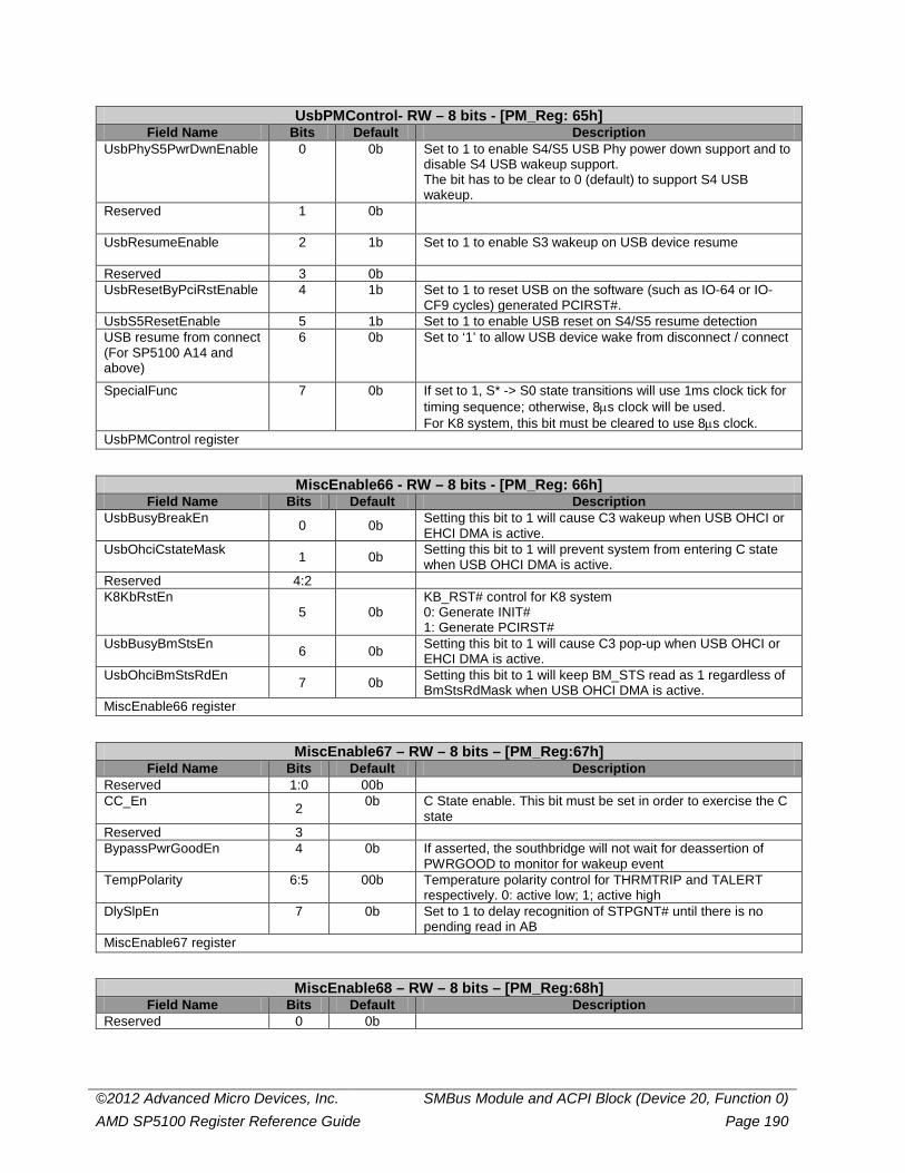
©2012 Advanced Micro Devices, Inc. SMBus Module and ACPI Block (Device 20, Function 0) AMD SP5100 Register Reference Guide Page 190
UsbPMControl- RW – 8 bits - [PM_Reg: 65h] Field Name Bits Default Description
UsbPhyS5PwrDwnEnable
0 0b Set to 1 to enable S4/S5 USB Phy power down support and to disable S4 USB wakeup support. The bit has to be clear to 0 (default) to support S4 USB wakeup.
Reserved
1 0b
UsbResumeEnable
2 1b Set to 1 to enable S3 wakeup on USB device resume
Reserved 3 0b UsbResetByPciRstEnable 4 1b Set to 1 to reset USB on the software (such as IO-64 or IO-
CF9 cycles) generated PCIRST#. UsbS5ResetEnable 5 1b Set to 1 to enable USB reset on S4/S5 resume detection USB resume from connect (For SP5100 A14 and above)
6 0b Set to ‘1’ to allow USB device wake from disconnect / connect
SpecialFunc
7 0b If set to 1, S* -> S0 state transitions will use 1ms clock tick for timing sequence; otherwise, 8µs clock will be used. For K8 system, this bit must be cleared to use 8µs clock.
UsbPMControl register
MiscEnable66 - RW – 8 bits - [PM_Reg: 66h] Field Name Bits Default Description
UsbBusyBreakEn 0 0b Setting this bit to 1 will cause C3 wakeup when USB OHCI or EHCI DMA is active.
UsbOhciCstateMask 1 0b Setting this bit to 1 will prevent system from entering C state when USB OHCI DMA is active.
Reserved 4:2 K8KbRstEn
5 0b KB_RST# control for K8 system 0: Generate INIT# 1: Generate PCIRST#
UsbBusyBmStsEn 6 0b Setting this bit to 1 will cause C3 pop-up when USB OHCI or EHCI DMA is active.
UsbOhciBmStsRdEn 7 0b Setting this bit to 1 will keep BM_STS read as 1 regardless of BmStsRdMask when USB OHCI DMA is active.
MiscEnable66 register
MiscEnable67 – RW – 8 bits – [PM_Reg:67h] Field Name Bits Default Description
Reserved 1:0 00b CC_En 2 0b C State enable. This bit must be set in order to exercise the C
state Reserved 3 BypassPwrGoodEn 4 0b If asserted, the southbridge will not wait for deassertion of
PWRGOOD to monitor for wakeup event TempPolarity 6:5 00b Temperature polarity control for THRMTRIP and TALERT
respectively. 0: active low; 1; active high DlySlpEn 7 0b Set to 1 to delay recognition of STPGNT# until there is no
pending read in AB MiscEnable67 register
MiscEnable68 – RW – 8 bits – [PM_Reg:68h] Field Name Bits Default Description
Reserved 0 0b
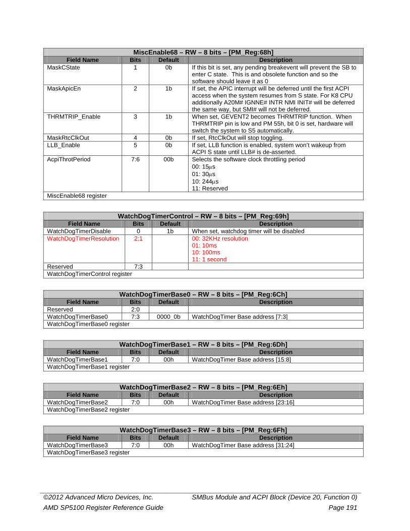
©2012 Advanced Micro Devices, Inc. SMBus Module and ACPI Block (Device 20, Function 0) AMD SP5100 Register Reference Guide Page 191
MiscEnable68 – RW – 8 bits – [PM_Reg:68h] Field Name Bits Default Description
MaskCState 1 0b If this bit is set, any pending breakevent will prevent the SB to enter C state. This is and obsolete function and so the software should leave it as 0
MaskApicEn 2 1b If set, the APIC interrupt will be deferred until the first ACPI access when the system resumes from S state. For K8 CPU additionally A20M# IGNNE# INTR NMI INIT# will be deferred the same way, but SMI# will not be deferred.
THRMTRIP_Enable 3 1b When set, GEVENT2 becomes THRMTRIP function. When THRMTRIP pin is low and PM 55h, bit 0 is set, hardware will switch the system to S5 automatically.
MaskRtcClkOut 4 0b If set, RtcClkOut will stop toggling. LLB_Enable 5 0b If set, LLB function is enabled, system won’t wakeup from
ACPI S state until LLB# is de-asserted. AcpiThrotPeriod 7:6 00b Selects the software clock throttling period
00: 15µs 01: 30µs 10: 244µs 11: Reserved
MiscEnable68 register
WatchDogTimerControl – RW – 8 bits – [PM_Reg:69h] Field Name Bits Default Description
WatchDogTimerDisable 0 1b When set, watchdog timer will be disabled WatchDogTimerResolution 2:1 00: 32KHz resolution
01: 10ms 10: 100ms 11: 1 second
Reserved 7:3 WatchDogTimerControl register
WatchDogTimerBase0 – RW – 8 bits – [PM_Reg:6Ch] Field Name Bits Default Description
Reserved 2:0 WatchDogTimerBase0 7:3 0000_0b WatchDogTimer Base address [7:3] WatchDogTimerBase0 register
WatchDogTimerBase1 – RW – 8 bits – [PM_Reg:6Dh] Field Name Bits Default Description
WatchDogTimerBase1 7:0 00h WatchDogTimer Base address [15:8] WatchDogTimerBase1 register
WatchDogTimerBase2 – RW – 8 bits – [PM_Reg:6Eh] Field Name Bits Default Description
WatchDogTimerBase2 7:0 00h WatchDogTimer Base address [23:16] WatchDogTimerBase2 register
WatchDogTimerBase3 – RW – 8 bits – [PM_Reg:6Fh] Field Name Bits Default Description
WatchDogTimerBase3 7:0 00h WatchDogTimer Base address [31:24] WatchDogTimerBase3 register
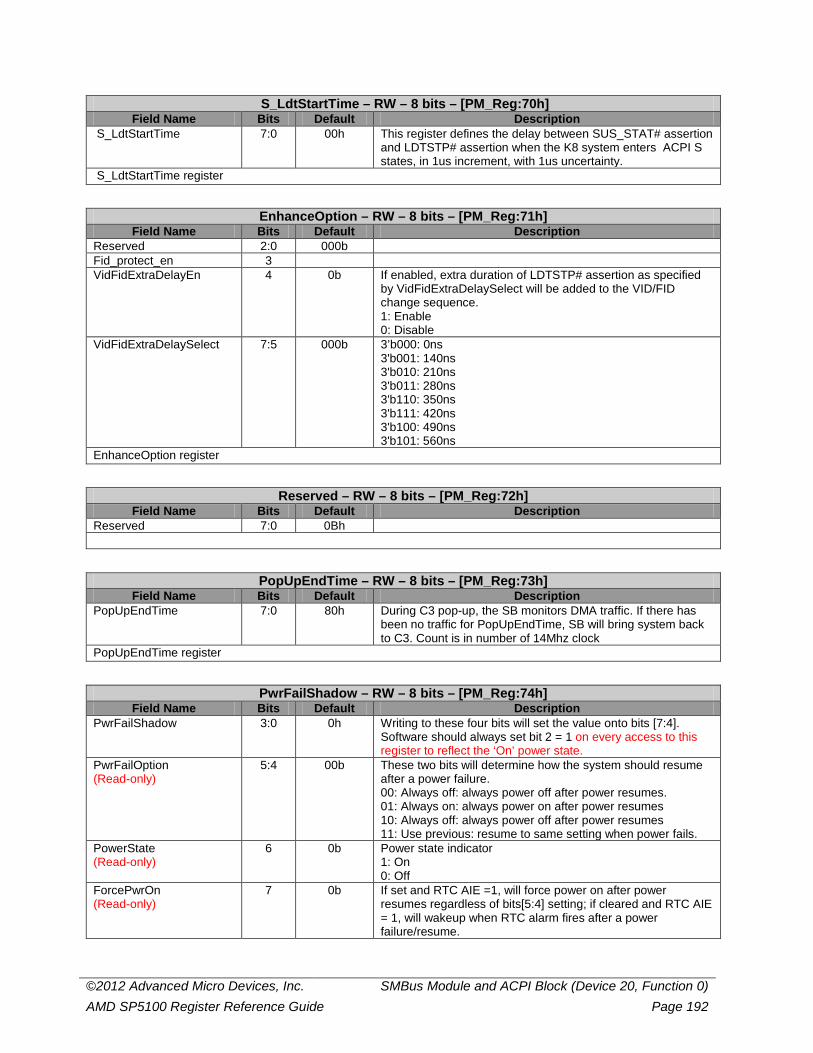
©2012 Advanced Micro Devices, Inc. SMBus Module and ACPI Block (Device 20, Function 0) AMD SP5100 Register Reference Guide Page 192
S_LdtStartTime – RW – 8 bits – [PM_Reg:70h] Field Name Bits Default Description
S_LdtStartTime 7:0 00h This register defines the delay between SUS_STAT# assertion and LDTSTP# assertion when the K8 system enters ACPI S states, in 1us increment, with 1us uncertainty.
S_LdtStartTime register
EnhanceOption – RW – 8 bits – [PM_Reg:71h] Field Name Bits Default Description
Reserved 2:0 000b Fid_protect_en 3 VidFidExtraDelayEn 4 0b If enabled, extra duration of LDTSTP# assertion as specified
by VidFidExtraDelaySelect will be added to the VID/FID change sequence. 1: Enable 0: Disable
VidFidExtraDelaySelect 7:5 000b 3’b000: 0ns 3'b001: 140ns 3'b010: 210ns 3'b011: 280ns 3'b110: 350ns 3'b111: 420ns 3'b100: 490ns 3'b101: 560ns
EnhanceOption register
Reserved – RW – 8 bits – [PM_Reg:72h] Field Name Bits Default Description
Reserved 7:0 0Bh
PopUpEndTime – RW – 8 bits – [PM_Reg:73h] Field Name Bits Default Description
PopUpEndTime 7:0 80h During C3 pop-up, the SB monitors DMA traffic. If there has been no traffic for PopUpEndTime, SB will bring system back to C3. Count is in number of 14Mhz clock
PopUpEndTime register
PwrFailShadow – RW – 8 bits – [PM_Reg:74h] Field Name Bits Default Description
PwrFailShadow 3:0 0h Writing to these four bits will set the value onto bits [7:4]. Software should always set bit 2 = 1 on every access to this register to reflect the ‘On’ power state.
PwrFailOption (Read-only)
5:4 00b These two bits will determine how the system should resume after a power failure. 00: Always off: always power off after power resumes. 01: Always on: always power on after power resumes 10: Always off: always power off after power resumes 11: Use previous: resume to same setting when power fails.
PowerState (Read-only)
6 0b Power state indicator 1: On 0: Off
ForcePwrOn (Read-only)
7 0b If set and RTC AIE =1, will force power on after power resumes regardless of bits[5:4] setting; if cleared and RTC AIE = 1, will wakeup when RTC alarm fires after a power failure/resume.
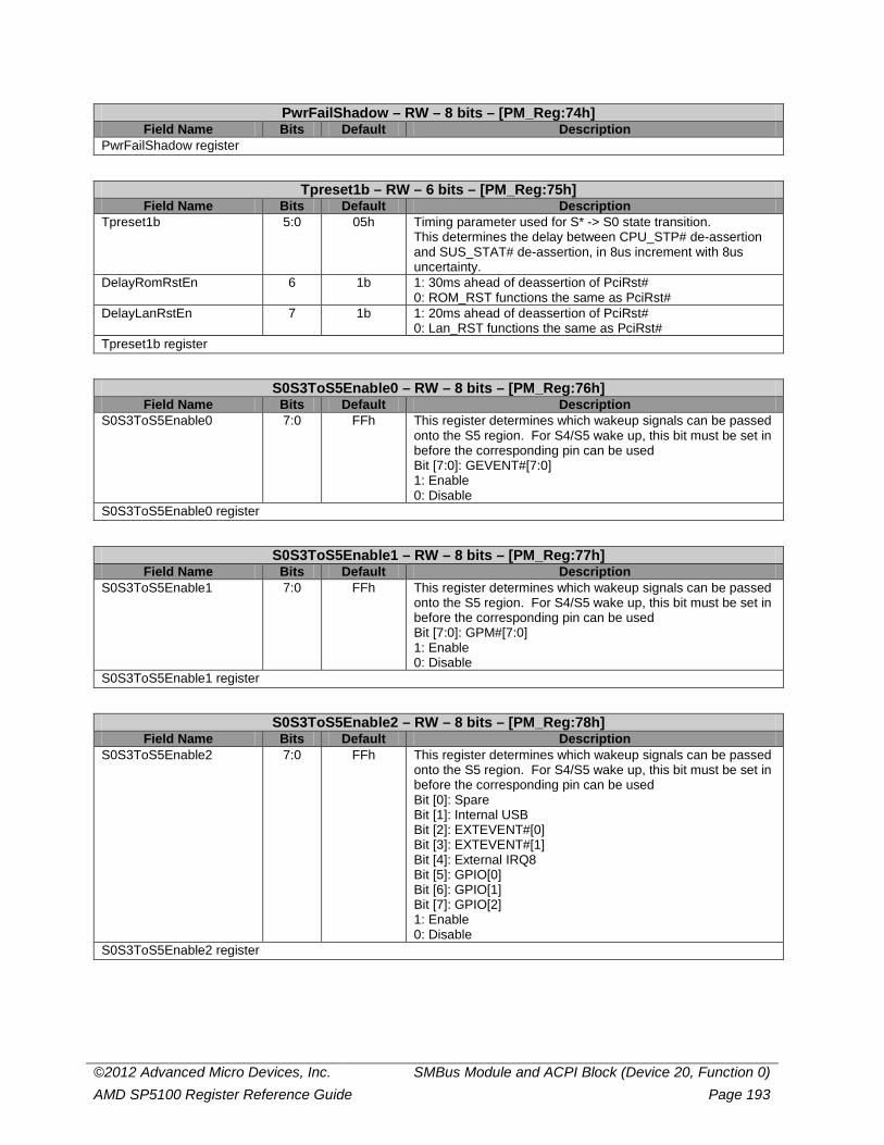
©2012 Advanced Micro Devices, Inc. SMBus Module and ACPI Block (Device 20, Function 0) AMD SP5100 Register Reference Guide Page 193
PwrFailShadow – RW – 8 bits – [PM_Reg:74h] Field Name Bits Default Description
PwrFailShadow register
Tpreset1b – RW – 6 bits – [PM_Reg:75h] Field Name Bits Default Description
Tpreset1b 5:0 05h Timing parameter used for S* -> S0 state transition. This determines the delay between CPU_STP# de-assertion and SUS_STAT# de-assertion, in 8us increment with 8us uncertainty.
DelayRomRstEn 6 1b 1: 30ms ahead of deassertion of PciRst# 0: ROM_RST functions the same as PciRst#
DelayLanRstEn 7 1b 1: 20ms ahead of deassertion of PciRst# 0: Lan_RST functions the same as PciRst#
Tpreset1b register
S0S3ToS5Enable0 – RW – 8 bits – [PM_Reg:76h] Field Name Bits Default Description
S0S3ToS5Enable0 7:0 FFh This register determines which wakeup signals can be passed onto the S5 region. For S4/S5 wake up, this bit must be set in before the corresponding pin can be used Bit [7:0]: GEVENT#[7:0] 1: Enable 0: Disable
S0S3ToS5Enable0 register
S0S3ToS5Enable1 – RW – 8 bits – [PM_Reg:77h] Field Name Bits Default Description
S0S3ToS5Enable1 7:0 FFh This register determines which wakeup signals can be passed onto the S5 region. For S4/S5 wake up, this bit must be set in before the corresponding pin can be used Bit [7:0]: GPM#[7:0] 1: Enable 0: Disable
S0S3ToS5Enable1 register
S0S3ToS5Enable2 – RW – 8 bits – [PM_Reg:78h] Field Name Bits Default Description
S0S3ToS5Enable2 7:0 FFh This register determines which wakeup signals can be passed onto the S5 region. For S4/S5 wake up, this bit must be set in before the corresponding pin can be used Bit [0]: Spare Bit [1]: Internal USB Bit [2]: EXTEVENT#[0] Bit [3]: EXTEVENT#[1] Bit [4]: External IRQ8 Bit [5]: GPIO[0] Bit [6]: GPIO[1] Bit [7]: GPIO[2] 1: Enable 0: Disable
S0S3ToS5Enable2 register
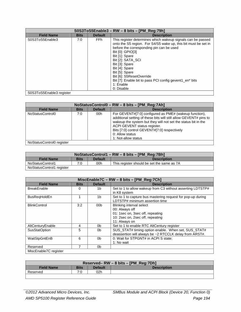
©2012 Advanced Micro Devices, Inc. SMBus Module and ACPI Block (Device 20, Function 0) AMD SP5100 Register Reference Guide Page 194
S0S3ToS5Enable3 – RW – 8 bits – [PM_Reg:79h] Field Name Bits Default Description
S0S3ToS5Enable3 7:0 FFh This register determines which wakeup signals can be passed onto the S5 region. For S4/S5 wake up, this bit must be set in before the corresponding pin can be used Bit [0]: GPIO[3] Bit [1]: Spare Bit [2]: SATA_SCI Bit [3]: Spare Bit [4]: Spare Bit [5]: Spare Bit [6]: S5ResetOverride Bit [7]: Enable bit to pass PCI config gevent1_en* bits 1: Enable 0: Disable
S0S3ToS5Enable3 register
NoStatusControl0 – RW – 8 bits – [PM_Reg:7Ah] Field Name Bits Default Description
NoStatusControl0 7:0 00h For GEVENT#[7:0] configured as PME# (wakeup function), additional setting of these bits will still allow GEVENT# pins to wakeup the system but they will not set the status bit in the ACPI GEVENT status register. Bits [7:0] control GEVENT#[7:0] respectively 0: Allow status 1: Not-allow status
NoStatusControl0 register
NoStatusControl1 – RW – 8 bits – [PM_Reg:7Bh] Field Name Bits Default Description
NoStatusControl1 7:0 00h This register should be set the same as 7A NoStatusControl1 register
MiscEnable7C – RW – 8 bits – [PM_Reg:7Ch] Field Name Bits Default Description
BreakEnable 0 1b Set to 1 to allow wakeup from C3 without asserting LDTSTP# in K8 system
BusReqHoldEn 1 1b Set to 1 to capture bus mastering request for pop-up during LDTSTP# minimum assertion time
BlinkControl 3:2 00b Blinking interval select 00: Always off 01: 1sec on, 3sec off, repeating 10: 2sec on, 2sec off, repeating 11: Always on
AltCenturyEnable 4 0b Set to 1 to enable RTC AltCentury register SusStatOption 5 0b SUS_STAT# timing option enable. When set, SUS_STAT#
deassertion will always be ~2 RTCCLK delay from ARST#. WaitStpGntEnB 6 0b 0: Wait for STPGNT# in ACPI S state;
1: No wait Reserved 7 0b MiscEnable7C register
Reserved– RW – 8 bits – [PM_Reg:7Dh] Field Name Bits Default Description
Reserved 7:0 02h
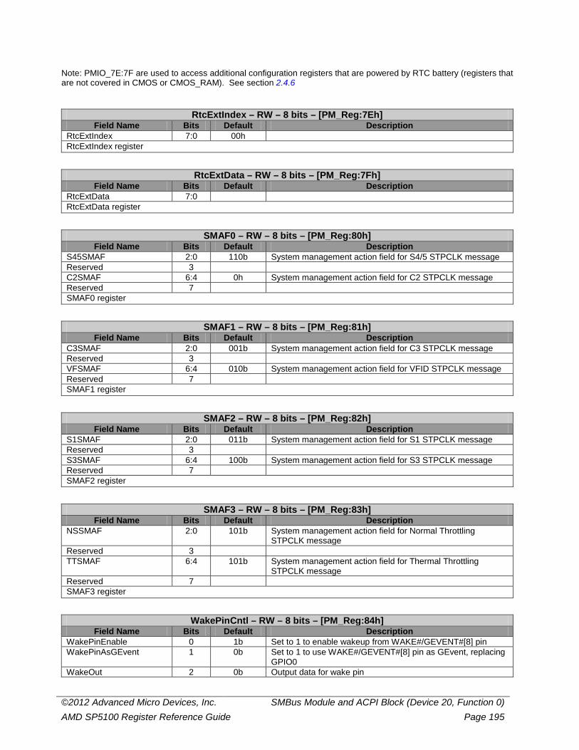
©2012 Advanced Micro Devices, Inc. SMBus Module and ACPI Block (Device 20, Function 0) AMD SP5100 Register Reference Guide Page 195
Note: PMIO_7E:7F are used to access additional configuration registers that are powered by RTC battery (registers that are not covered in CMOS or CMOS_RAM). See section 2.4.6
RtcExtIndex – RW – 8 bits – [PM_Reg:7Eh] Field Name Bits Default Description
RtcExtIndex 7:0 00h RtcExtIndex register
RtcExtData – RW – 8 bits – [PM_Reg:7Fh] Field Name Bits Default Description
RtcExtData 7:0 RtcExtData register
SMAF0 – RW – 8 bits – [PM_Reg:80h] Field Name Bits Default Description
S45SMAF 2:0 110b System management action field for S4/5 STPCLK message Reserved 3 C2SMAF 6:4 0h System management action field for C2 STPCLK message Reserved 7 SMAF0 register
SMAF1 – RW – 8 bits – [PM_Reg:81h] Field Name Bits Default Description
C3SMAF 2:0 001b System management action field for C3 STPCLK message Reserved 3 VFSMAF 6:4 010b System management action field for VFID STPCLK message Reserved 7 SMAF1 register
SMAF2 – RW – 8 bits – [PM_Reg:82h] Field Name Bits Default Description
S1SMAF 2:0 011b System management action field for S1 STPCLK message Reserved 3 S3SMAF 6:4 100b System management action field for S3 STPCLK message Reserved 7 SMAF2 register
SMAF3 – RW – 8 bits – [PM_Reg:83h] Field Name Bits Default Description
NSSMAF 2:0 101b System management action field for Normal Throttling STPCLK message
Reserved 3 TTSMAF 6:4 101b System management action field for Thermal Throttling
STPCLK message Reserved 7 SMAF3 register
WakePinCntl – RW – 8 bits – [PM_Reg:84h] Field Name Bits Default Description
WakePinEnable 0 1b Set to 1 to enable wakeup from WAKE#/GEVENT#[8] pin WakePinAsGEvent 1 0b Set to 1 to use WAKE#/GEVENT#[8] pin as GEvent, replacing
GPIO0 WakeOut 2 0b Output data for wake pin
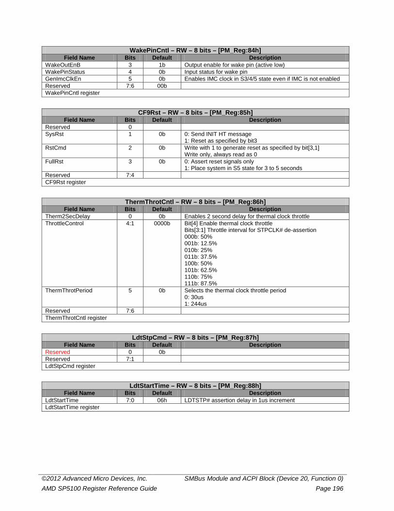
©2012 Advanced Micro Devices, Inc. SMBus Module and ACPI Block (Device 20, Function 0) AMD SP5100 Register Reference Guide Page 196
WakePinCntl – RW – 8 bits – [PM_Reg:84h] Field Name Bits Default Description
WakeOutEnB 3 1b Output enable for wake pin (active low) WakePinStatus 4 0b Input status for wake pin GenImcClkEn 5 0b Enables IMC clock in S3/4/5 state even if IMC is not enabled Reserved 7:6 00b WakePinCntl register
CF9Rst – RW – 8 bits – [PM_Reg:85h] Field Name Bits Default Description
Reserved 0 SysRst 1 0b 0: Send INIT HT message
1: Reset as specified by bit3 RstCmd 2 0b Write with 1 to generate reset as specified by bit[3,1]
Write only, always read as 0 FullRst 3 0b 0: Assert reset signals only
1: Place system in S5 state for 3 to 5 seconds Reserved 7:4 CF9Rst register
ThermThrotCntl – RW – 8 bits – [PM_Reg:86h] Field Name Bits Default Description
Therm2SecDelay 0 0b Enables 2 second delay for thermal clock throttle ThrottleControl 4:1 0000b Bit[4] Enable thermal clock throttle
Bits[3:1] Throttle interval for STPCLK# de-assertion 000b: 50% 001b: 12.5% 010b: 25% 011b: 37.5% 100b: 50% 101b: 62.5% 110b: 75% 111b: 87.5%
ThermThrotPeriod 5 0b Selects the thermal clock throttle period 0: 30us 1: 244us
Reserved 7:6 ThermThrotCntl register
LdtStpCmd – RW – 8 bits – [PM_Reg:87h] Field Name Bits Default Description
Reserved 0 0b Reserved 7:1 LdtStpCmd register
LdtStartTime – RW – 8 bits – [PM_Reg:88h] Field Name Bits Default Description
LdtStartTime 7:0 06h LDTSTP# assertion delay in 1us increment LdtStartTime register
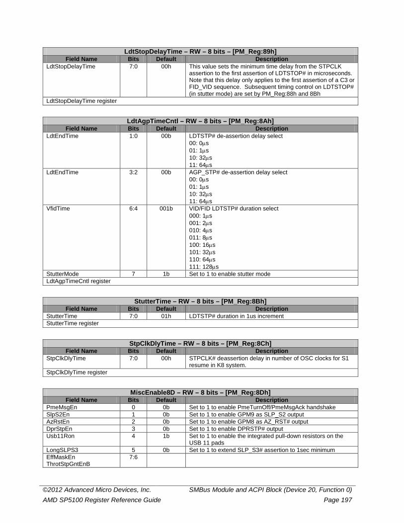
©2012 Advanced Micro Devices, Inc. SMBus Module and ACPI Block (Device 20, Function 0) AMD SP5100 Register Reference Guide Page 197
LdtStopDelayTime – RW – 8 bits – [PM_Reg:89h] Field Name Bits Default Description
LdtStopDelayTime 7:0 00h This value sets the minimum time delay from the STPCLK assertion to the first assertion of LDTSTOP# in microseconds. Note that this delay only applies to the first assertion of a C3 or FID_VID sequence. Subsequent timing control on LDTSTOP# (in stutter mode) are set by PM_Reg:88h and 8Bh
LdtStopDelayTime register
LdtAgpTimeCntl – RW – 8 bits – [PM_Reg:8Ah] Field Name Bits Default Description
LdtEndTime 1:0 00b LDTSTP# de-assertion delay select 00: 0µs 01: 1µs 10: 32µs 11: 64µs
LdtEndTime 3:2 00b AGP_STP# de-assertion delay select 00: 0µs 01: 1µs 10: 32µs 11: 64µs
VfidTime 6:4 001b VID/FID LDTSTP# duration select 000: 1µs 001: 2µs 010: 4µs 011: 8µs 100: 16µs 101: 32µs 110: 64µs 111: 128µs
StutterMode 7 1b Set to 1 to enable stutter mode LdtAgpTimeCntl register
StutterTime – RW – 8 bits – [PM_Reg:8Bh] Field Name Bits Default Description
StutterTime 7:0 01h LDTSTP# duration in 1us increment StutterTime register
StpClkDlyTime – RW – 8 bits – [PM_Reg:8Ch] Field Name Bits Default Description
StpClkDlyTime 7:0 00h STPCLK# deassertion delay in number of OSC clocks for S1 resume in K8 system.
StpClkDlyTime register
MiscEnable8D – RW – 8 bits – [PM_Reg:8Dh] Field Name Bits Default Description
PmeMsgEn 0 0b Set to 1 to enable PmeTurnOff/PmeMsgAck handshake SlpS2En 1 0b Set to 1 to enable GPM9 as SLP_S2 output AzRstEn 2 0b Set to 1 to enable GPM8 as AZ_RST# output DprStpEn 3 0b Set to 1 to enable DPRSTP# output Usb11Ron 4 1b Set to 1 to enable the integrated pull-down resistors on the
USB 11 pads LongSLPS3 5 0b Set to 1 to extend SLP_S3# assertion to 1sec minimum EffMaskEn ThrotStpGntEnB
7:6
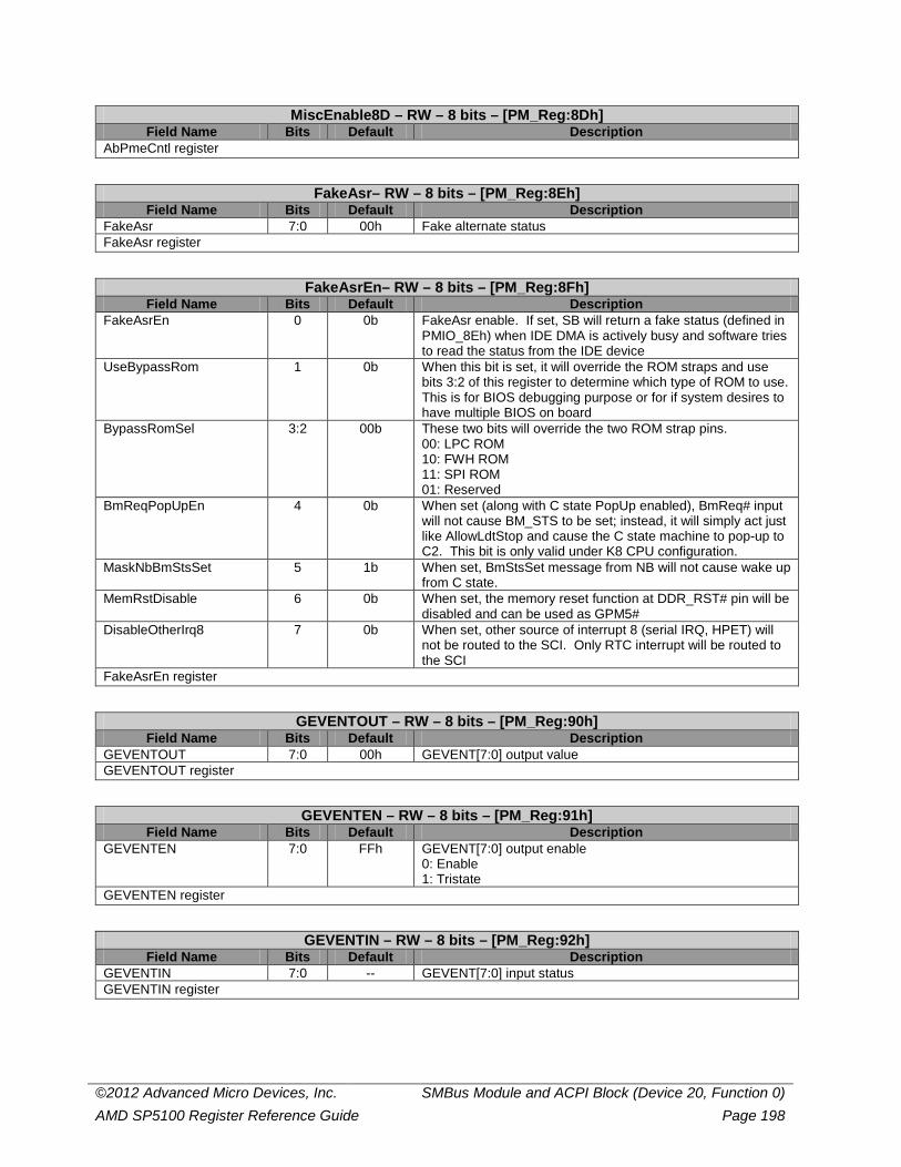
©2012 Advanced Micro Devices, Inc. SMBus Module and ACPI Block (Device 20, Function 0) AMD SP5100 Register Reference Guide Page 198
MiscEnable8D – RW – 8 bits – [PM_Reg:8Dh] Field Name Bits Default Description
AbPmeCntl register
FakeAsr– RW – 8 bits – [PM_Reg:8Eh] Field Name Bits Default Description
FakeAsr 7:0 00h Fake alternate status FakeAsr register
FakeAsrEn– RW – 8 bits – [PM_Reg:8Fh] Field Name Bits Default Description
FakeAsrEn 0 0b FakeAsr enable. If set, SB will return a fake status (defined in PMIO_8Eh) when IDE DMA is actively busy and software tries to read the status from the IDE device
UseBypassRom 1 0b When this bit is set, it will override the ROM straps and use bits 3:2 of this register to determine which type of ROM to use. This is for BIOS debugging purpose or for if system desires to have multiple BIOS on board
BypassRomSel 3:2 00b These two bits will override the two ROM strap pins. 00: LPC ROM 10: FWH ROM 11: SPI ROM 01: Reserved
BmReqPopUpEn 4 0b When set (along with C state PopUp enabled), BmReq# input will not cause BM_STS to be set; instead, it will simply act just like AllowLdtStop and cause the C state machine to pop-up to C2. This bit is only valid under K8 CPU configuration.
MaskNbBmStsSet 5 1b When set, BmStsSet message from NB will not cause wake up from C state.
MemRstDisable 6 0b When set, the memory reset function at DDR_RST# pin will be disabled and can be used as GPM5#
DisableOtherIrq8 7 0b When set, other source of interrupt 8 (serial IRQ, HPET) will not be routed to the SCI. Only RTC interrupt will be routed to the SCI
FakeAsrEn register
GEVENTOUT – RW – 8 bits – [PM_Reg:90h] Field Name Bits Default Description
GEVENTOUT 7:0 00h GEVENT[7:0] output value GEVENTOUT register
GEVENTEN – RW – 8 bits – [PM_Reg:91h] Field Name Bits Default Description
GEVENTEN 7:0 FFh GEVENT[7:0] output enable 0: Enable 1: Tristate
GEVENTEN register
GEVENTIN – RW – 8 bits – [PM_Reg:92h] Field Name Bits Default Description
GEVENTIN 7:0 -- GEVENT[7:0] input status GEVENTIN register
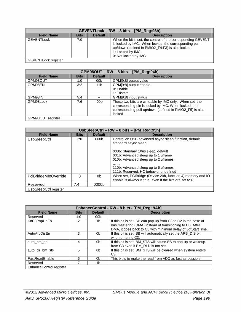
©2012 Advanced Micro Devices, Inc. SMBus Module and ACPI Block (Device 20, Function 0) AMD SP5100 Register Reference Guide Page 199
GEVENTLock – RW – 8 bits – [PM_Reg:93h] Field Name Bits Default Description
GEVENTLock 7:0 -- When the bit is set, the control of the corresponding GEVENT is locked by IMC. When locked, the corresponding pull-up/down (defined in PMIO2_F4:F3) is also locked. 1: Locked by IMC 0: Not locked by IMC
GEVENTLock register
GPM98OUT – RW – 8 bits – [PM_Reg:94h] Field Name Bits Default Description
GPM98OUT 1:0 00b GPM[9:8] output value GPM98EN 3:2 11b GPM[9:8] output enable
0: Enable 1: Tristate
GPM98IN 5:4 -- GPM[9:8] input status GPM98Lock 7:6 00b These two bits are writeable by IMC only. When set, the
corresponding pin is locked by IMC. When locked, the corresponding pull-up/down (defined in PMIO2_F5) is also locked
GPM98OUT register
UsbSleepCtrl – RW – 8 bits – [PM_Reg:95h] Field Name Bits Default Description
UsbSleepCtrl 2:0 000b Control on USB advanced async sleep function, default standard async sleep. 000b: Standard 10us sleep, default 001b: Advanced sleep up to 1 uframe 010b: Advanced sleep up to 2 uframes …… 110b: Advanced sleep up to 6 uframes 111b: Reserved, HC behavior undefined
PciBridgeMIoOverride 3 0b When set, PCIBridge (Device 20h, function 4) memory and IO enable is always is true; even if the bits are set to 0
Reserved 7:4 0000b UsbSleepCtrl register
EnhanceControl - RW - 8 bits - [PM_Reg: 9Ah] Field Name Bits Default Description
Reserved 1:0 00b K8C3PopUpEn 2 1b If this bit is set, SB can pop up from C3 to C2 in the case of
bus mastering (DMA) instead of transitioning to C0. After DMA, it goes back to C3 with minimum delay of LdtStartTime.
AutoArbDisEn 3 0b If this bit is set, SB will automatically set the ARB_DIS bit when entering C3.
auto_bm_rld 4 0b If this bit is set, BM_STS will cause SB to pop-up or wakeup from C3 even if BM_RLD is not set.
auto_clr_bm_sts 5 0b If this bit is set, BM_STS will be cleared when system enters C3.
FastReadEnable 6 0b This bit is to make the read from ADC as fast as possible. Reserved 7 1b EnhanceControl register
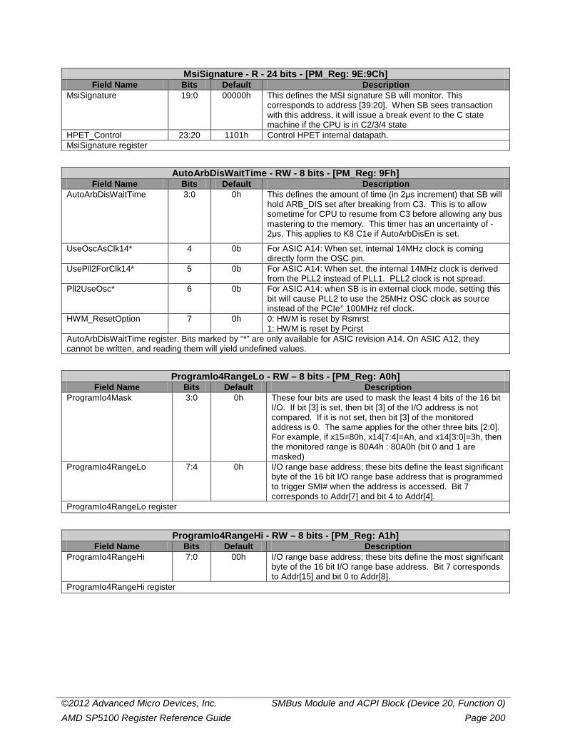
©2012 Advanced Micro Devices, Inc. SMBus Module and ACPI Block (Device 20, Function 0) AMD SP5100 Register Reference Guide Page 200
MsiSignature - R - 24 bits - [PM_Reg: 9E:9Ch] Field Name Bits Default Description
MsiSignature 19:0 00000h This defines the MSI signature SB will monitor. This corresponds to address [39:20]. When SB sees transaction with this address, it will issue a break event to the C state machine if the CPU is in C2/3/4 state
HPET_Control 23:20 1101h Control HPET internal datapath. MsiSignature register
AutoArbDisWaitTime - RW - 8 bits - [PM_Reg: 9Fh] Field Name Bits Default Description
AutoArbDisWaitTime 3:0 0h This defines the amount of time (in 2μs increment) that SB will hold ARB_DIS set after breaking from C3. This is to allow sometime for CPU to resume from C3 before allowing any bus mastering to the memory. This timer has an uncertainty of -2μs. This applies to K8 C1e if AutoArbDisEn is set.
UseOscAsClk14* 4 0b For ASIC A14: When set, internal 14MHz clock is coming directly form the OSC pin.
UsePll2ForClk14* 5 0b For ASIC A14: When set, the internal 14MHz clock is derived from the PLL2 instead of PLL1. PLL2 clock is not spread.
Pll2UseOsc* 6 0b For ASIC A14: when SB is in external clock mode, setting this bit will cause PLL2 to use the 25MHz OSC clock as source instead of the PCIe 100MHz ref clock.
HWM_ResetOption 7 0h 0: HWM is reset by Rsmrst 1: HWM is reset by Pcirst
AutoArbDisWaitTime register. Bits marked by “*” are only available for ASIC revision A14. On ASIC A12, they cannot be written, and reading them will yield undefined values.
Programlo4RangeLo - RW – 8 bits - [PM_Reg: A0h] Field Name Bits Default Description
ProgramIo4Mask 3:0 0h These four bits are used to mask the least 4 bits of the 16 bit I/O. If bit [3] is set, then bit [3] of the I/O address is not compared. If it is not set, then bit [3] of the monitored address is 0. The same applies for the other three bits [2:0]. For example, if x15=80h, x14[7:4]=Ah, and x14[3:0]=3h, then the monitored range is 80A4h : 80A0h (bit 0 and 1 are masked)
ProgramIo4RangeLo 7:4 0h I/O range base address; these bits define the least significant byte of the 16 bit I/O range base address that is programmed to trigger SMI# when the address is accessed. Bit 7 corresponds to Addr[7] and bit 4 to Addr[4].
ProgramIo4RangeLo register
ProgramIo4RangeHi - RW – 8 bits - [PM_Reg: A1h] Field Name Bits Default Description
ProgramIo4RangeHi 7:0 00h I/O range base address; these bits define the most significant byte of the 16 bit I/O range base address. Bit 7 corresponds to Addr[15] and bit 0 to Addr[8].
ProgramIo4RangeHi register
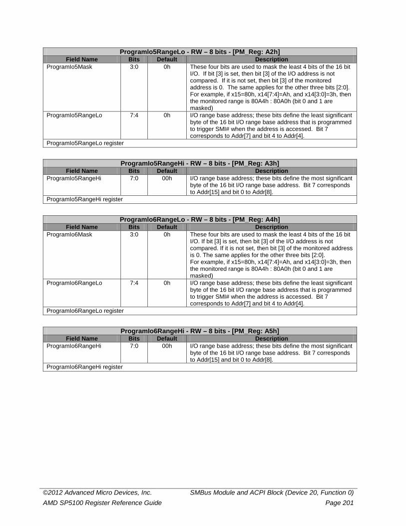
©2012 Advanced Micro Devices, Inc. SMBus Module and ACPI Block (Device 20, Function 0) AMD SP5100 Register Reference Guide Page 201
Programlo5RangeLo - RW – 8 bits - [PM_Reg: A2h] Field Name Bits Default Description
ProgramIo5Mask 3:0 0h These four bits are used to mask the least 4 bits of the 16 bit I/O. If bit [3] is set, then bit [3] of the I/O address is not compared. If it is not set, then bit [3] of the monitored address is 0. The same applies for the other three bits [2:0]. For example, if x15=80h, x14[7:4]=Ah, and x14[3:0]=3h, then the monitored range is 80A4h : 80A0h (bit 0 and 1 are masked)
ProgramIo5RangeLo 7:4 0h I/O range base address; these bits define the least significant byte of the 16 bit I/O range base address that is programmed to trigger SMI# when the address is accessed. Bit 7 corresponds to Addr[7] and bit 4 to Addr[4].
ProgramIo5RangeLo register
ProgramIo5RangeHi - RW – 8 bits - [PM_Reg: A3h] Field Name Bits Default Description
ProgramIo5RangeHi 7:0 00h I/O range base address; these bits define the most significant byte of the 16 bit I/O range base address. Bit 7 corresponds to Addr[15] and bit 0 to Addr[8].
ProgramIo5RangeHi register
Programlo6RangeLo - RW – 8 bits - [PM_Reg: A4h] Field Name Bits Default Description
ProgramIo6Mask 3:0 0h These four bits are used to mask the least 4 bits of the 16 bit I/O. If bit [3] is set, then bit [3] of the I/O address is not compared. If it is not set, then bit [3] of the monitored address is 0. The same applies for the other three bits [2:0]. For example, if x15=80h, x14[7:4]=Ah, and x14[3:0]=3h, then the monitored range is 80A4h : 80A0h (bit 0 and 1 are masked)
ProgramIo6RangeLo 7:4 0h I/O range base address; these bits define the least significant byte of the 16 bit I/O range base address that is programmed to trigger SMI# when the address is accessed. Bit 7 corresponds to Addr[7] and bit 4 to Addr[4].
ProgramIo6RangeLo register
ProgramIo6RangeHi - RW – 8 bits - [PM_Reg: A5h] Field Name Bits Default Description
ProgramIo6RangeHi 7:0 00h I/O range base address; these bits define the most significant byte of the 16 bit I/O range base address. Bit 7 corresponds to Addr[15] and bit 0 to Addr[8].
ProgramIo6RangeHi register
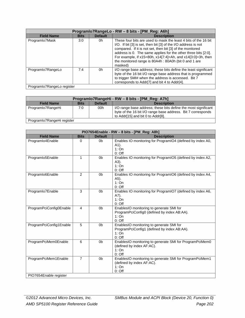
©2012 Advanced Micro Devices, Inc. SMBus Module and ACPI Block (Device 20, Function 0) AMD SP5100 Register Reference Guide Page 202
Programlo7RangeLo - RW – 8 bits - [PM_Reg: A6h] Field Name Bits Default Description
ProgramIo7Mask 3:0 0h These four bits are used to mask the least 4 bits of the 16 bit I/O. If bit [3] is set, then bit [3] of the I/O address is not compared. If it is not set, then bit [3] of the monitored address is 0. The same applies for the other three bits [2:0]. For example, if x15=80h, x14[7:4]=Ah, and x14[3:0]=3h, then the monitored range is 80A4h : 80A0h (bit 0 and 1 are masked)
ProgramIo7RangeLo 7:4 0h I/O range base address; these bits define the least significant byte of the 16 bit I/O range base address that is programmed to trigger SMI# when the address is accessed. Bit 7 corresponds to Addr[7] and bit 4 to Addr[4].
ProgramIo7RangeLo register
ProgramIo7RangeHi - RW – 8 bits - [PM_Reg: A7h] Field Name Bits Default Description
ProgramIo7RangeHi 7:0 00h I/O range base address; these bits define the most significant byte of the 16 bit I/O range base address. Bit 7 corresponds to Addr[15] and bit 0 to Addr[8].
ProgramIo7RangeHi register
PIO7654Enable - RW – 8 bits - [PM_Reg: A8h] Field Name Bits Default Description
ProgramIo4Enable 0 0b Enables IO monitoring for ProgramIO4 (defined by index A0, A1). 1: On 0: Off
ProgramIo5Enable 1 0b Enables IO monitoring for ProgramIO5 (defined by index A2, A3). 1: On 0: Off
ProgramIo6Enable 2 0b Enables IO monitoring for ProgramIO6 (defined by index A4, A5). 1: On 0: Off
ProgramIo7Enable 3 0b Enables IO monitoring for ProgramIO7 (defined by index A6, A7). 1: On 0: Off
ProgramPciConfig0Enable 4 0b EnablesIO monitoring to generate SMI for ProgramPciConfig0 (defined by index AB:AA). 1: On 0: Off
ProgramPciConfig1Enable 5 0b EnablesIO monitoring to generate SMI for ProgramPciConfig1 (defined by index AB:AA). 1: On 0: Off
ProgramPciMem0Enable 6 0b EnablesIO monitoring to generate SMI for ProgramPciMem0 (defined by index AF:AC). 1: On 0: Off
ProgramPciMem1Enable 7 0b EnablesIO monitoring to generate SMI for ProgramPciMem1 (defined by index AF:AC). 1: On 0: Off
PIO7654Enable register
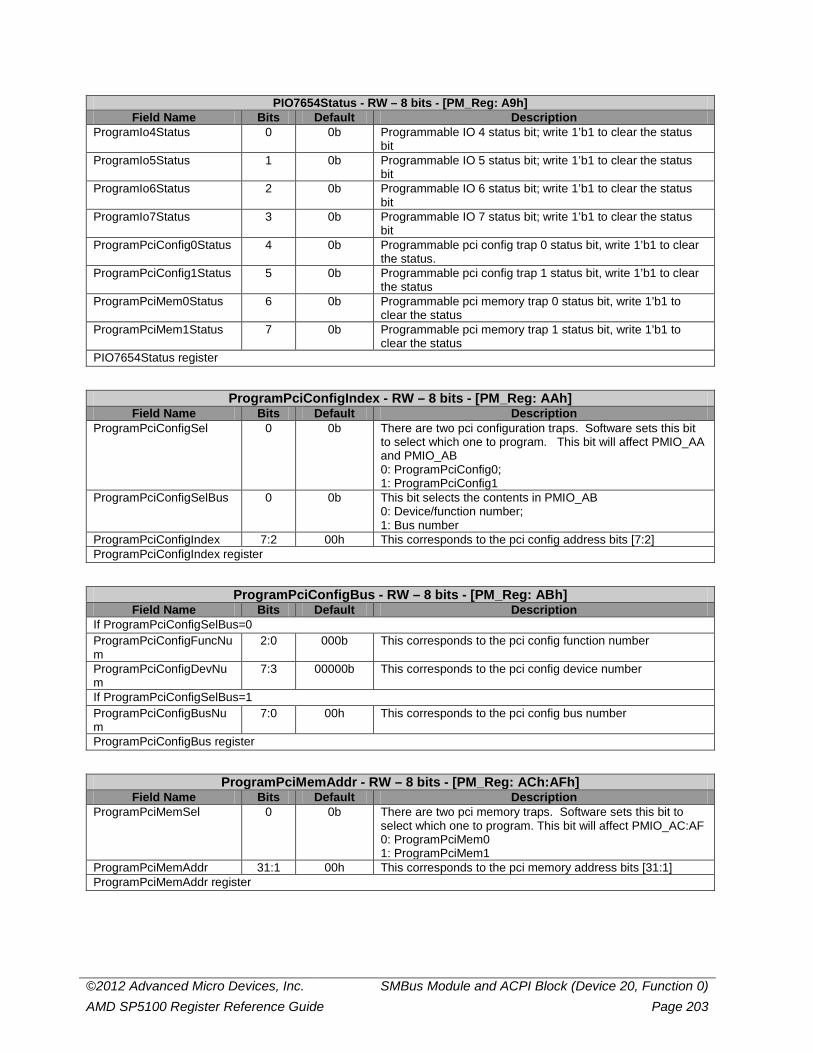
©2012 Advanced Micro Devices, Inc. SMBus Module and ACPI Block (Device 20, Function 0) AMD SP5100 Register Reference Guide Page 203
PIO7654Status - RW – 8 bits - [PM_Reg: A9h] Field Name Bits Default Description
ProgramIo4Status 0 0b Programmable IO 4 status bit; write 1’b1 to clear the status bit
ProgramIo5Status 1 0b Programmable IO 5 status bit; write 1’b1 to clear the status bit
ProgramIo6Status 2 0b Programmable IO 6 status bit; write 1’b1 to clear the status bit
ProgramIo7Status
3 0b Programmable IO 7 status bit; write 1’b1 to clear the status bit
ProgramPciConfig0Status 4 0b Programmable pci config trap 0 status bit, write 1’b1 to clear the status.
ProgramPciConfig1Status 5 0b Programmable pci config trap 1 status bit, write 1’b1 to clear the status
ProgramPciMem0Status 6 0b Programmable pci memory trap 0 status bit, write 1’b1 to clear the status
ProgramPciMem1Status 7 0b Programmable pci memory trap 1 status bit, write 1’b1 to clear the status
PIO7654Status register
ProgramPciConfigIndex - RW – 8 bits - [PM_Reg: AAh] Field Name Bits Default Description
ProgramPciConfigSel 0 0b There are two pci configuration traps. Software sets this bit to select which one to program. This bit will affect PMIO_AA and PMIO_AB 0: ProgramPciConfig0; 1: ProgramPciConfig1
ProgramPciConfigSelBus 0 0b This bit selects the contents in PMIO_AB 0: Device/function number; 1: Bus number
ProgramPciConfigIndex 7:2 00h This corresponds to the pci config address bits [7:2] ProgramPciConfigIndex register
ProgramPciConfigBus - RW – 8 bits - [PM_Reg: ABh] Field Name Bits Default Description
If ProgramPciConfigSelBus=0 ProgramPciConfigFuncNum
2:0 000b This corresponds to the pci config function number
ProgramPciConfigDevNum
7:3 00000b This corresponds to the pci config device number
If ProgramPciConfigSelBus=1 ProgramPciConfigBusNum
7:0 00h This corresponds to the pci config bus number
ProgramPciConfigBus register
ProgramPciMemAddr - RW – 8 bits - [PM_Reg: ACh:AFh] Field Name Bits Default Description
ProgramPciMemSel 0 0b There are two pci memory traps. Software sets this bit to select which one to program. This bit will affect PMIO_AC:AF 0: ProgramPciMem0 1: ProgramPciMem1
ProgramPciMemAddr 31:1 00h This corresponds to the pci memory address bits [31:1] ProgramPciMemAddr register
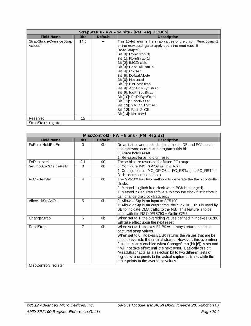
©2012 Advanced Micro Devices, Inc. SMBus Module and ACPI Block (Device 20, Function 0) AMD SP5100 Register Reference Guide Page 204
StrapStatus - RW – 24 bits - [PM_Reg:B1:B0h] Field Name Bits Default Description
StrapStatus/OverrideStrapValues
14:0 -- This 15-bit returns the strap values of the chip if ReadStrap=1 or the new settings to apply upon the next reset if ReadStrap=0. Bit [0]: RomStrap[0] Bit [1]: RomStrap[1] Bit [2]: IMCEnable Bit [3]: BootFailTmrEn Bit [4]: ClkGen Bit [5]: DefaultMode Bit [6]: Not used Bit [7]: I2cRomStrap Bit [8]: AcpiBclkBypStrap Bit [9]: IdePllBypStrap Bit [10]: PciPllBypStrap Bit [11]: ShortReset Bit [12]: SATAClkSrcFlip Bit [13]: Fast I2cClk Bit [14]: Not used
Reserved 15 StrapStatus register
MiscControl3 - RW – 8 bits - [PM_Reg:B2] Field Name Bits Default Description
FcForceHoldRstEn 0 0b Default at power on this bit force holds IDE and FC’s reset, until software comes and programs this bit. 0: Force holds reset 1: Releases force hold on reset
FcReserved 2:1 00 These bits are reserved for future FC usage SetImcGpio3AsIdeRstB 3 0b 0: Configure IMC_GPIO3 as IDE_RST#
1: Configure it as IMC_GPIO3 or FC_RST# (it is FC_RST# if flash controller is enabled)
FcClkGenSel 4 0b The SP5100 has two methods to generate the flash controller clocks. 0: Method 1 (glitch free clock when BCh is changed) 1: Method 2 (requires software to stop the clock first before it can change the clock frequency)
AllowLdtStpAsOut 5 0b 0: AllowLdtStp is an input to SP5100 1: AllowLdtStp is an output from the SP5100. This is used by SB to indicate DMA traffic to the NB. This feature is to be used with the RS740/RS790 + Griffin CPU
ChangeStrap 6 0b When set to 1, the overriding values defined in indexes B1:B0 will take effect upon the next reset.
ReadStrap 7 0b When set to 1, indexes B1:B0 will always return the actual captured strap values. When set to 0, indexes B1:B0 returns the values that are be used to override the original straps. However, this overriding function is only enabled when ChangeStrap (bit [6]) is set and it will not take effect until the next reset. Basically this bit “ReadStrap” acts as a selection bit to two different sets of registers; one points to the actual captured straps while the other points to the overriding values.
MiscControl3 register
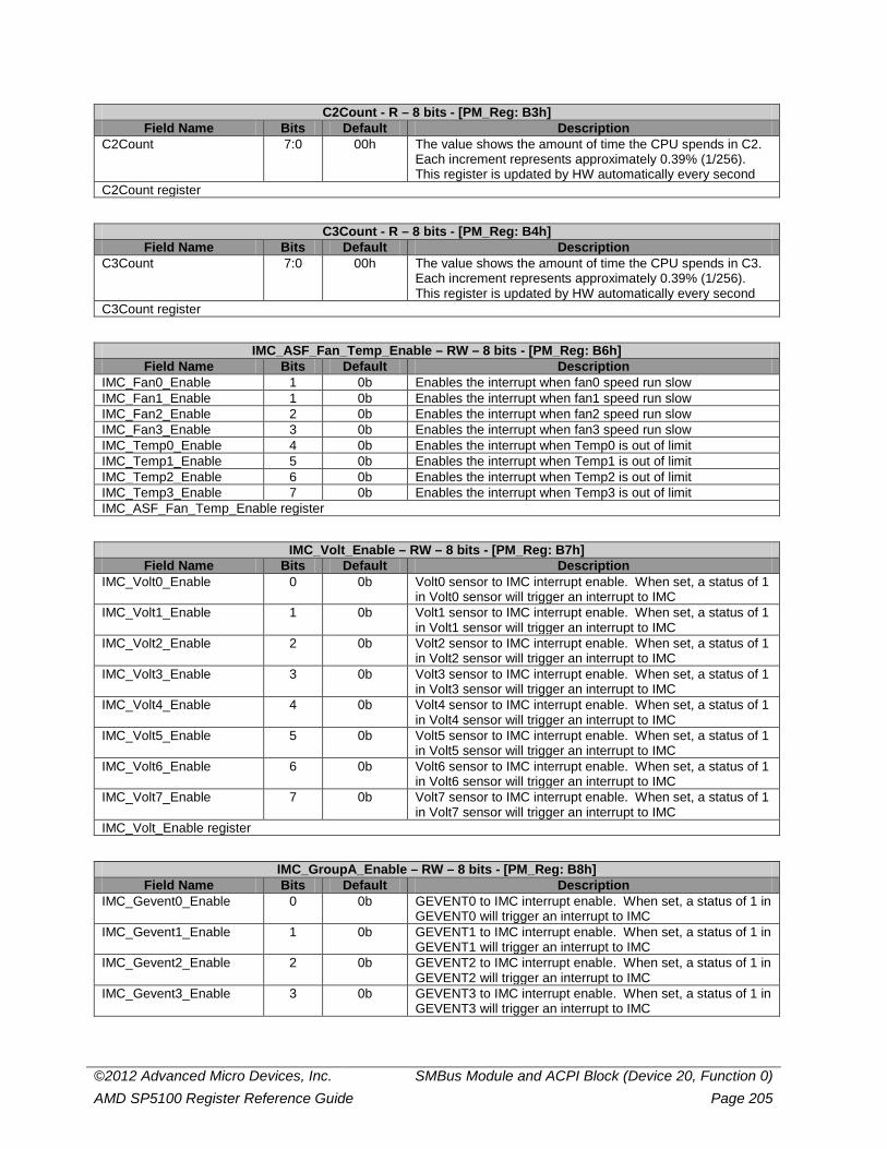
©2012 Advanced Micro Devices, Inc. SMBus Module and ACPI Block (Device 20, Function 0) AMD SP5100 Register Reference Guide Page 205
C2Count - R – 8 bits - [PM_Reg: B3h] Field Name Bits Default Description
C2Count 7:0 00h The value shows the amount of time the CPU spends in C2. Each increment represents approximately 0.39% (1/256). This register is updated by HW automatically every second
C2Count register
C3Count - R – 8 bits - [PM_Reg: B4h] Field Name Bits Default Description
C3Count 7:0 00h The value shows the amount of time the CPU spends in C3. Each increment represents approximately 0.39% (1/256). This register is updated by HW automatically every second
C3Count register
IMC_ASF_Fan_Temp_Enable – RW – 8 bits - [PM_Reg: B6h] Field Name Bits Default Description
IMC_Fan0_Enable 1 0b Enables the interrupt when fan0 speed run slow IMC_Fan1_Enable 1 0b Enables the interrupt when fan1 speed run slow IMC_Fan2_Enable 2 0b Enables the interrupt when fan2 speed run slow IMC_Fan3_Enable 3 0b Enables the interrupt when fan3 speed run slow IMC_Temp0_Enable 4 0b Enables the interrupt when Temp0 is out of limit IMC_Temp1_Enable 5 0b Enables the interrupt when Temp1 is out of limit IMC_Temp2_Enable 6 0b Enables the interrupt when Temp2 is out of limit IMC_Temp3_Enable 7 0b Enables the interrupt when Temp3 is out of limit IMC_ASF_Fan_Temp_Enable register
IMC_Volt_Enable – RW – 8 bits - [PM_Reg: B7h] Field Name Bits Default Description
IMC_Volt0_Enable 0 0b Volt0 sensor to IMC interrupt enable. When set, a status of 1 in Volt0 sensor will trigger an interrupt to IMC
IMC_Volt1_Enable 1 0b Volt1 sensor to IMC interrupt enable. When set, a status of 1 in Volt1 sensor will trigger an interrupt to IMC
IMC_Volt2_Enable 2 0b Volt2 sensor to IMC interrupt enable. When set, a status of 1 in Volt2 sensor will trigger an interrupt to IMC
IMC_Volt3_Enable 3 0b Volt3 sensor to IMC interrupt enable. When set, a status of 1 in Volt3 sensor will trigger an interrupt to IMC
IMC_Volt4_Enable 4 0b Volt4 sensor to IMC interrupt enable. When set, a status of 1 in Volt4 sensor will trigger an interrupt to IMC
IMC_Volt5_Enable 5 0b Volt5 sensor to IMC interrupt enable. When set, a status of 1 in Volt5 sensor will trigger an interrupt to IMC
IMC_Volt6_Enable 6 0b Volt6 sensor to IMC interrupt enable. When set, a status of 1 in Volt6 sensor will trigger an interrupt to IMC
IMC_Volt7_Enable 7 0b Volt7 sensor to IMC interrupt enable. When set, a status of 1 in Volt7 sensor will trigger an interrupt to IMC
IMC_Volt_Enable register
IMC_GroupA_Enable – RW – 8 bits - [PM_Reg: B8h] Field Name Bits Default Description
IMC_Gevent0_Enable 0 0b GEVENT0 to IMC interrupt enable. When set, a status of 1 in GEVENT0 will trigger an interrupt to IMC
IMC_Gevent1_Enable 1 0b GEVENT1 to IMC interrupt enable. When set, a status of 1 in GEVENT1 will trigger an interrupt to IMC
IMC_Gevent2_Enable 2 0b GEVENT2 to IMC interrupt enable. When set, a status of 1 in GEVENT2 will trigger an interrupt to IMC
IMC_Gevent3_Enable 3 0b GEVENT3 to IMC interrupt enable. When set, a status of 1 in GEVENT3 will trigger an interrupt to IMC
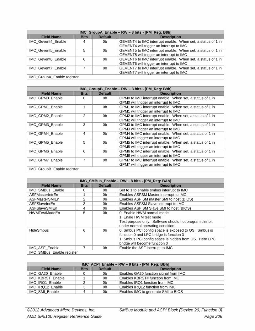
©2012 Advanced Micro Devices, Inc. SMBus Module and ACPI Block (Device 20, Function 0) AMD SP5100 Register Reference Guide Page 206
IMC_GroupA_Enable – RW – 8 bits - [PM_Reg: B8h] Field Name Bits Default Description
IMC_Gevent4_Enable 4 0b GEVENT4 to IMC interrupt enable. When set, a status of 1 in GEVENT4 will trigger an interrupt to IMC
IMC_Gevent5_Enable 5 0b GEVENT5 to IMC interrupt enable. When set, a status of 1 in GEVENT5 will trigger an interrupt to IMC
IMC_Gevent6_Enable 6 0b GEVENT6 to IMC interrupt enable. When set, a status of 1 in GEVENT6 will trigger an interrupt to IMC
IMC_Gevent7_Enable 7 0b GEVENT7 to IMC interrupt enable. When set, a status of 1 in GEVENT7 will trigger an interrupt to IMC
IMC_GroupA_Enable register
IMC_GroupB_Enable – RW – 8 bits - [PM_Reg: B9h] Field Name Bits Default Description
IMC_GPM0_Enable 0 0b GPM0 to IMC interrupt enable. When set, a status of 1 in GPM0 will trigger an interrupt to IMC
IMC_GPM1_Enable 1 0b GPM1 to IMC interrupt enable. When set, a status of 1 in GPM1 will trigger an interrupt to IMC
IMC_GPM2_Enable 2 0b GPM2 to IMC interrupt enable. When set, a status of 1 in GPM2 will trigger an interrupt to IMC
IMC_GPM3_Enable 3 0b GPM3 to IMC interrupt enable. When set, a status of 1 in GPM3 will trigger an interrupt to IMC
IMC_GPM4_Enable 4 0b GPM4 to IMC interrupt enable. When set, a status of 1 in GPM4 will trigger an interrupt to IMC
IMC_GPM5_Enable 5 0b GPM5 to IMC interrupt enable. When set, a status of 1 in GPM5 will trigger an interrupt to IMC
IMC_GPM6_Enable 6 0b GPM6 to IMC interrupt enable. When set, a status of 1 in GPM6 will trigger an interrupt to IMC
IMC_GPM7_Enable 7 0b GPM7 to IMC interrupt enable. When set, a status of 1 in GPM7 will trigger an interrupt to IMC
IMC_GroupB_Enable register
IMC_SMBus_Enable – RW – 8 bits - [PM_Reg: BAh] Field Name Bits Default Description
IMC_SMBus_Enable 0 0b Set to 1 to enable smbus interrupt to IMC ASFMasterIntrEn 1 0b Enables ASFSM Master interrupt to IMC ASFMasterSMIEn 2 0b Enables ASF SM master SMI to host (BIOS) ASFSlaveInrEn 3 0b Enables ASFSM Slave interrupt to IMC ASFSlaveSMIEn 4 0b Enables ASF SM Slave SMI to host (BIOS) HWMTestModeEn 5 0b 0: Enable HWM normal mode
1: Enale HWM test mode Test purpose only. Software should not program this bit under normal operating condition.
HideSmbus 6 0b 0: Smbus PCI config space is exposed to OS. Smbus is function 0 and LPC bridge is function 3 1: Smbus PCI config space is hidden from OS. Here LPC bridge will become function 0
IMC_ASF_Enable 7 0b Enable the ASF interrupt to IMC IMC_SMBus_Enable register
IMC_ACPI_Enable – RW – 8 bits - [PM_Reg: BBh] Field Name Bits Default Description
IMC_GA20_Enable 0 0b Enables GA20 function signal from IMC IMC_KBRST_Enable 1 0b Enables KBRST# function from IMC IMC_IRQ1_Enable 2 0b Enables IRQ1 function from IMC IMC_IRQ12_Enable 3 0b Enables IRQ12 function from IMC IMC_SMI_Enable 4 0b Enables IMC to generate SMI to BIOS
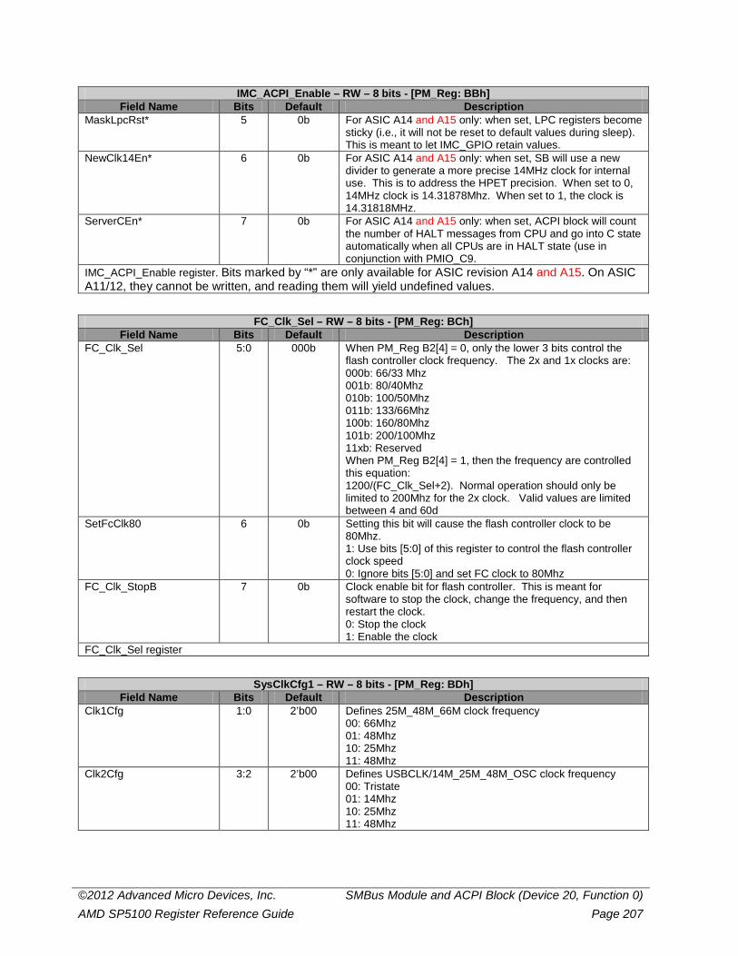
©2012 Advanced Micro Devices, Inc. SMBus Module and ACPI Block (Device 20, Function 0) AMD SP5100 Register Reference Guide Page 207
IMC_ACPI_Enable – RW – 8 bits - [PM_Reg: BBh] Field Name Bits Default Description
MaskLpcRst* 5 0b For ASIC A14 and A15 only: when set, LPC registers become sticky (i.e., it will not be reset to default values during sleep). This is meant to let IMC_GPIO retain values.
NewClk14En* 6 0b For ASIC A14 and A15 only: when set, SB will use a new divider to generate a more precise 14MHz clock for internal use. This is to address the HPET precision. When set to 0, 14MHz clock is 14.31878Mhz. When set to 1, the clock is 14.31818MHz.
ServerCEn* 7 0b For ASIC A14 and A15 only: when set, ACPI block will count the number of HALT messages from CPU and go into C state automatically when all CPUs are in HALT state (use in conjunction with PMIO_C9.
IMC_ACPI_Enable register. Bits marked by “*” are only available for ASIC revision A14 and A15. On ASIC A11/12, they cannot be written, and reading them will yield undefined values.
FC_Clk_Sel – RW – 8 bits - [PM_Reg: BCh] Field Name Bits Default Description
FC_Clk_Sel 5:0 000b When PM_Reg B2[4] = 0, only the lower 3 bits control the flash controller clock frequency. The 2x and 1x clocks are: 000b: 66/33 Mhz 001b: 80/40Mhz 010b: 100/50Mhz 011b: 133/66Mhz 100b: 160/80Mhz 101b: 200/100Mhz 11xb: Reserved When PM_Reg B2[4] = 1, then the frequency are controlled this equation: 1200/(FC_Clk_Sel+2). Normal operation should only be limited to 200Mhz for the 2x clock. Valid values are limited between 4 and 60d
SetFcClk80 6 0b Setting this bit will cause the flash controller clock to be 80Mhz. 1: Use bits [5:0] of this register to control the flash controller clock speed 0: Ignore bits [5:0] and set FC clock to 80Mhz
FC_Clk_StopB 7 0b Clock enable bit for flash controller. This is meant for software to stop the clock, change the frequency, and then restart the clock. 0: Stop the clock 1: Enable the clock
FC_Clk_Sel register
SysClkCfg1 – RW – 8 bits - [PM_Reg: BDh] Field Name Bits Default Description
Clk1Cfg 1:0 2’b00 Defines 25M_48M_66M clock frequency 00: 66Mhz 01: 48Mhz 10: 25Mhz 11: 48Mhz
Clk2Cfg 3:2 2’b00 Defines USBCLK/14M_25M_48M_OSC clock frequency 00: Tristate 01: 14Mhz 10: 25Mhz 11: 48Mhz
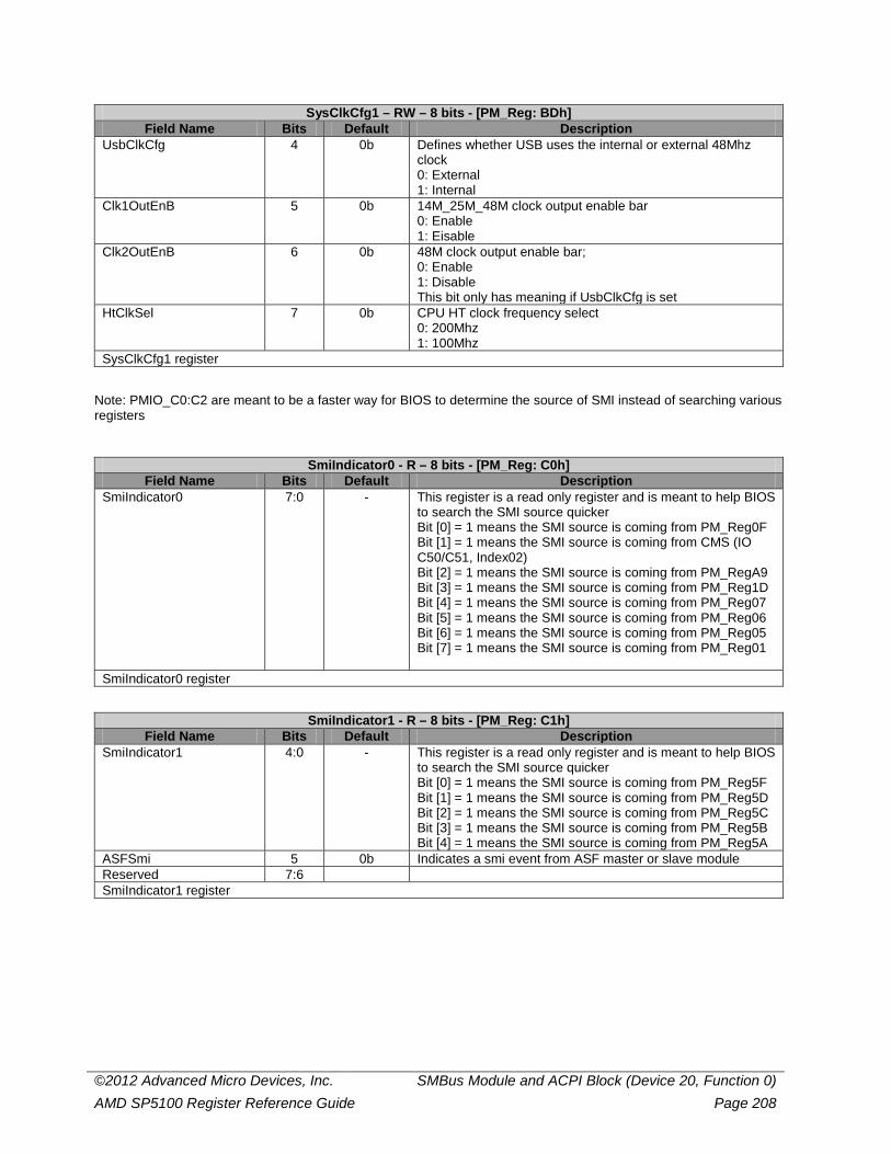
©2012 Advanced Micro Devices, Inc. SMBus Module and ACPI Block (Device 20, Function 0) AMD SP5100 Register Reference Guide Page 208
SysClkCfg1 – RW – 8 bits - [PM_Reg: BDh] Field Name Bits Default Description
UsbClkCfg 4 0b Defines whether USB uses the internal or external 48Mhz clock 0: External 1: Internal
Clk1OutEnB 5 0b 14M_25M_48M clock output enable bar 0: Enable 1: Eisable
Clk2OutEnB 6 0b 48M clock output enable bar; 0: Enable 1: Disable This bit only has meaning if UsbClkCfg is set
HtClkSel 7 0b CPU HT clock frequency select 0: 200Mhz 1: 100Mhz
SysClkCfg1 register
Note: PMIO_C0:C2 are meant to be a faster way for BIOS to determine the source of SMI instead of searching various registers
SmiIndicator0 - R – 8 bits - [PM_Reg: C0h] Field Name Bits Default Description
SmiIndicator0 7:0 - This register is a read only register and is meant to help BIOS to search the SMI source quicker Bit [0] = 1 means the SMI source is coming from PM_Reg0F Bit [1] = 1 means the SMI source is coming from CMS (IO C50/C51, Index02) Bit [2] = 1 means the SMI source is coming from PM_RegA9 Bit [3] = 1 means the SMI source is coming from PM_Reg1D Bit [4] = 1 means the SMI source is coming from PM_Reg07 Bit [5] = 1 means the SMI source is coming from PM_Reg06 Bit [6] = 1 means the SMI source is coming from PM_Reg05 Bit [7] = 1 means the SMI source is coming from PM_Reg01
SmiIndicator0 register
SmiIndicator1 - R – 8 bits - [PM_Reg: C1h] Field Name Bits Default Description
SmiIndicator1 4:0 - This register is a read only register and is meant to help BIOS to search the SMI source quicker Bit [0] = 1 means the SMI source is coming from PM_Reg5F Bit [1] = 1 means the SMI source is coming from PM_Reg5D Bit [2] = 1 means the SMI source is coming from PM_Reg5C Bit [3] = 1 means the SMI source is coming from PM_Reg5B Bit [4] = 1 means the SMI source is coming from PM_Reg5A
ASFSmi 5 0b Indicates a smi event from ASF master or slave module Reserved 7:6 SmiIndicator1 register
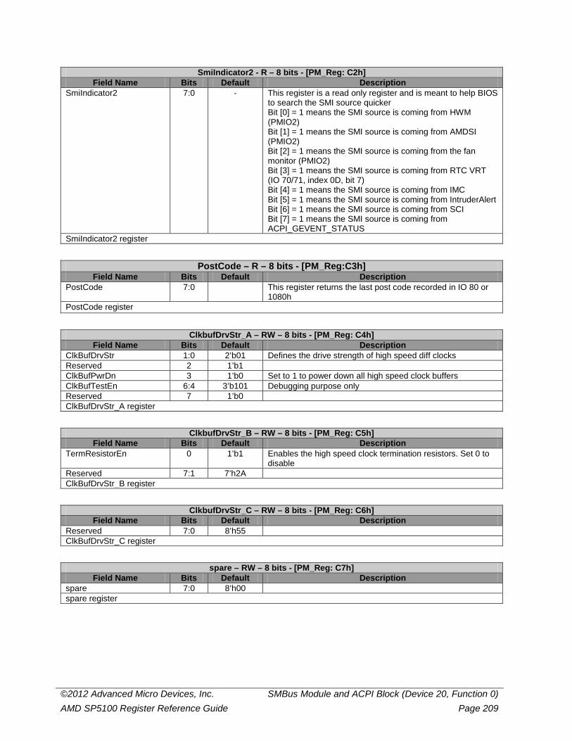
©2012 Advanced Micro Devices, Inc. SMBus Module and ACPI Block (Device 20, Function 0) AMD SP5100 Register Reference Guide Page 209
SmiIndicator2 - R – 8 bits - [PM_Reg: C2h] Field Name Bits Default Description
SmiIndicator2 7:0 - This register is a read only register and is meant to help BIOS to search the SMI source quicker Bit [0] = 1 means the SMI source is coming from HWM (PMIO2) Bit [1] = 1 means the SMI source is coming from AMDSI (PMIO2) Bit [2] = 1 means the SMI source is coming from the fan monitor (PMIO2) Bit [3] = 1 means the SMI source is coming from RTC VRT (IO 70/71, index 0D, bit 7) Bit [4] = 1 means the SMI source is coming from IMC Bit [5] = 1 means the SMI source is coming from IntruderAlert Bit [6] = 1 means the SMI source is coming from SCI Bit [7] = 1 means the SMI source is coming from ACPI_GEVENT_STATUS
SmiIndicator2 register
PostCode – R – 8 bits - [PM_Reg:C3h] Field Name Bits Default Description
PostCode 7:0 This register returns the last post code recorded in IO 80 or 1080h
PostCode register
ClkbufDrvStr_A – RW – 8 bits - [PM_Reg: C4h] Field Name Bits Default Description
ClkBufDrvStr 1:0 2’b01 Defines the drive strength of high speed diff clocks Reserved 2 1’b1 ClkBufPwrDn 3 1’b0 Set to 1 to power down all high speed clock buffers ClkBufTestEn 6:4 3’b101 Debugging purpose only Reserved 7 1’b0 ClkBufDrvStr_A register
ClkbufDrvStr_B – RW – 8 bits - [PM_Reg: C5h] Field Name Bits Default Description
TermResistorEn 0 1’b1 Enables the high speed clock termination resistors. Set 0 to disable
Reserved 7:1 7’h2A ClkBufDrvStr_B register
ClkbufDrvStr_C – RW – 8 bits - [PM_Reg: C6h] Field Name Bits Default Description
Reserved 7:0 8’h55 ClkBufDrvStr_C register
spare – RW – 8 bits - [PM_Reg: C7h] Field Name Bits Default Description
spare 7:0 8’h00 spare register
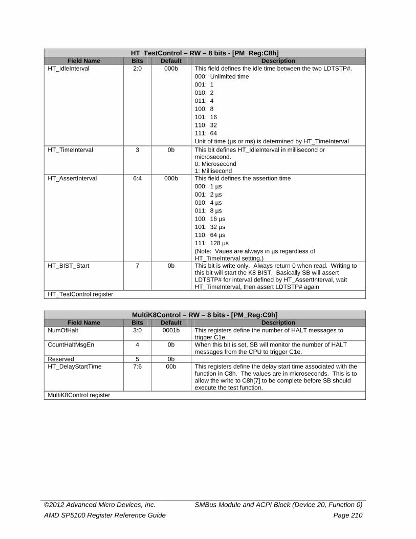
©2012 Advanced Micro Devices, Inc. SMBus Module and ACPI Block (Device 20, Function 0) AMD SP5100 Register Reference Guide Page 210
HT_TestControl – RW – 8 bits - [PM_Reg:C8h] Field Name Bits Default Description
HT_IdleInterval 2:0 000b This field defines the idle time between the two LDTSTP#. 000: Unlimited time 001: 1 010: 2 011: 4 100: 8 101: 16 110: 32 111: 64 Unit of time (µs or ms) is determined by HT_TimeInterval
HT_TimeInterval 3 0b This bit defines HT_IdleInterval in millisecond or microsecond. 0: Microsecond 1: Millisecond
HT_AssertInterval 6:4 000b This field defines the assertion time 000: 1 µs 001: 2 µs 010: 4 µs 011: 8 µs 100: 16 µs 101: 32 µs 110: 64 µs 111: 128 µs (Note: Vaues are always in µs regardless of HT_TimeInterval setting.)
HT_BIST_Start 7 0b This bit is write only. Always return 0 when read. Writing to this bit will start the K8 BIST. Basically SB will assert LDTSTP# for interval defined by HT_AssertInterval, wait HT_TimeInterval, then assert LDTSTP# again
HT_TestControl register
MultiK8Control – RW – 8 bits - [PM_Reg:C9h] Field Name Bits Default Description
NumOfHalt 3:0 0001b This registers define the number of HALT messages to trigger C1e.
CountHaltMsgEn 4 0b When this bit is set, SB will monitor the number of HALT messages from the CPU to trigger C1e.
Reserved 5 0b HT_DelayStartTime 7:6 00b This registers define the delay start time associated with the
function in C8h. The values are in microseconds. This is to allow the write to C8h[7] to be complete before SB should execute the test function.
MultiK8Control register
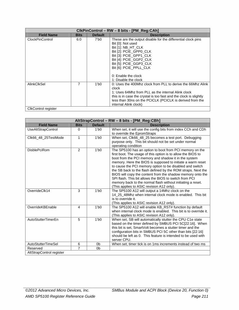
©2012 Advanced Micro Devices, Inc. SMBus Module and ACPI Block (Device 20, Function 0) AMD SP5100 Register Reference Guide Page 211
ClkPinControl – RW – 8 bits - [PM_Reg:CAh] Field Name Bits Default Description
ClockPinControl 6:0 7’b0 These are the output disable for the differential clock pins Bit [0]: Not used Bit [1]: NB_HT_CLK Bit [2]: PCIE_GPP0_CLK Bit [3]: PCIE_GPP1_CLK Bit [4]: PCIE_GGP2_CLK Bit [5]: PCIE_GGP3_CLK Bit [6]: PCIE_PPLL_CLK 0: Enable the clock 1: Disable the clock
AlinkClkSel 7 1’b0 0: Uses the 400Mhz clock from PLL to derive the 66Mhz Alink clock 1: Uses 64Mhz from PLL as the internal Alink clock this is in case the crystal is too fast and the clock is slightly less than 30ns on the PCICLK (PCICLK is derived from the internal Alink clock)
ClkControl register
AltStrapControl – RW – 8 bits - [PM_Reg:CBh] Field Name Bits Default Description
UseAltStrapControl 0 1’b0 When set, it will use the config bits from index CCh and CDh to override the EpromStraps
Clk66_48_25TestMode 1 1’b0 When set, Clk66_48_25 becomes a test port. Debugging purpose only. This bit should not be set under normal operating condition
DisblePciRom 2 1’b0 The SP5100 has an option to boot from PCI memory on the first boot. The usage of this option is to allow the BIOS to boot from the PCI memory and shadow it in the system memory. Here the BIOS is supposed to initiate a warm reset to cause the PCI memory option to be disabled and switch the SB back to the flash defined by the ROM straps. Next the BIOS will copy the content from the shadow memory onto the SPI flash. This bit allows the BIOS to switch from PCI memory back to the normal flash without initiating a reset. (This applies to ASIC revision A12 only).
OverrideClk14 3 1’b0 The SP5100 A12 will output a 14Mhz clock on the 14_25_48Mhz when internal clock mode is enabled. This bit is to override it. (This applies to ASIC revision A12 only).
OverrideKBEnable 4 1’b0 The SP5100 A12 will enable KB_RST# function by default when internal clock mode is enabled. This bit is to override it. (This applies to ASIC revision A12 only).
AutoStutterTimerEn 5 1’b0 When set, SB will automatically stutter the CPU C1e state based on the timer defined by SMBUS PCI 5C[22:16]. When this bit is set, SmartVolt becomes a stutter timer and the configuration bits in SMBUS PCI 5C other than bits [22:16] should be left as 0. This feature is intended to be used with server CPU.
AutoStutterTimeSel 6 0b When set, timer tick is on 1ms increments instead of two ms Reserved 7 0b AltStrapControl register
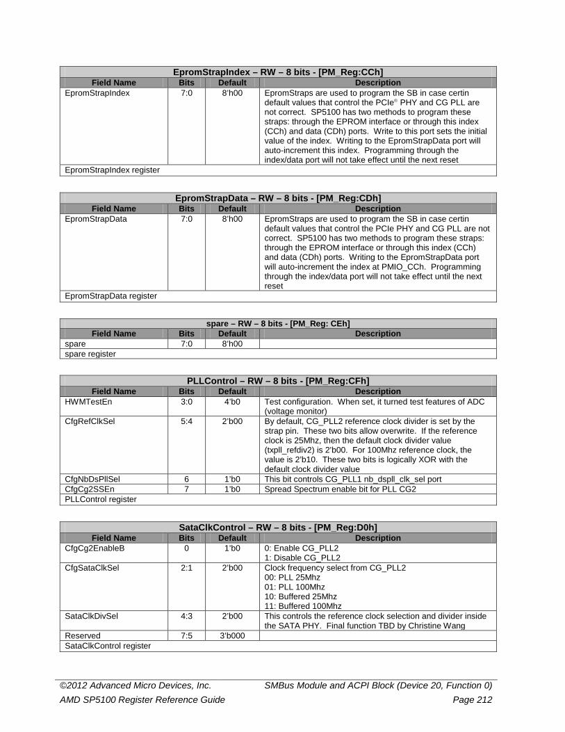
©2012 Advanced Micro Devices, Inc. SMBus Module and ACPI Block (Device 20, Function 0) AMD SP5100 Register Reference Guide Page 212
EpromStrapIndex – RW – 8 bits - [PM_Reg:CCh] Field Name Bits Default Description
EpromStrapIndex 7:0 8’h00 EpromStraps are used to program the SB in case certin default values that control the PCIe PHY and CG PLL are not correct. SP5100 has two methods to program these straps: through the EPROM interface or through this index (CCh) and data (CDh) ports. Write to this port sets the initial value of the index. Writing to the EpromStrapData port will auto-increment this index. Programming through the index/data port will not take effect until the next reset
EpromStrapIndex register
EpromStrapData – RW – 8 bits - [PM_Reg:CDh] Field Name Bits Default Description
EpromStrapData 7:0 8’h00 EpromStraps are used to program the SB in case certin default values that control the PCIe PHY and CG PLL are not correct. SP5100 has two methods to program these straps: through the EPROM interface or through this index (CCh) and data (CDh) ports. Writing to the EpromStrapData port will auto-increment the index at PMIO_CCh. Programming through the index/data port will not take effect until the next reset
EpromStrapData register
spare – RW – 8 bits - [PM_Reg: CEh] Field Name Bits Default Description
spare 7:0 8’h00 spare register
PLLControl – RW – 8 bits - [PM_Reg:CFh] Field Name Bits Default Description
HWMTestEn 3:0 4’b0 Test configuration. When set, it turned test features of ADC (voltage monitor)
CfgRefClkSel 5:4 2’b00 By default, CG_PLL2 reference clock divider is set by the strap pin. These two bits allow overwrite. If the reference clock is 25Mhz, then the default clock divider value (txpll_refdiv2) is 2’b00. For 100Mhz reference clock, the value is 2’b10. These two bits is logically XOR with the default clock divider value
CfgNbDsPllSel 6 1’b0 This bit controls CG_PLL1 nb_dspll_clk_sel port CfgCg2SSEn 7 1’b0 Spread Spectrum enable bit for PLL CG2 PLLControl register
SataClkControl – RW – 8 bits - [PM_Reg:D0h] Field Name Bits Default Description
CfgCg2EnableB 0 1’b0 0: Enable CG_PLL2 1: Disable CG_PLL2
CfgSataClkSel 2:1 2’b00 Clock frequency select from CG_PLL2 00: PLL 25Mhz 01: PLL 100Mhz 10: Buffered 25Mhz 11: Buffered 100Mhz
SataClkDivSel 4:3 2’b00 This controls the reference clock selection and divider inside the SATA PHY. Final function TBD by Christine Wang
Reserved 7:5 3’b000 SataClkControl register

©2012 Advanced Micro Devices, Inc. SMBus Module and ACPI Block (Device 20, Function 0) AMD SP5100 Register Reference Guide Page 213
PLLParameter1 – RW – 8 bits - [PM_Reg:D1h] Field Name Bits Default Description
CgPll1_Pcie_ClkEnB_Invert 0 1’b0 0: Use the strap value to determine whether PCIe 100Mhz clock should be enabled from CG PLL1. Normally PCIe clock is disabled when SB is strapped to use external clock and enabled when strapped to integrated clock 1: Invert the strap value that controls the PCIe clock enable bit
CgPll1_Ht_ClkEnB_Invert 1 1’b0 0: Use the strap value to determine whether HT 200Mhz clock should be enabled from CG PLL1. Normally this clock is disabled when SB is strapped to use external clock and enabled when strapped to integrated clock 1: Invert the strap value that controls the CPU HT clock enable bit
CgPll1_Test_ClkEnB 2 1’b0 0: Enable the CG PLL1 test node for probing 1: Disale the CG PLL1 test node for probing
CgPll1_IdePci_ClkEnB 3 1’b0 0: Enable CG PLL1 400Mhz clock 1: Disable CG PLL1 400Mhz clock
CgPll1_Alink_ClkEnB 4 1’b0 0: Enable the 64Mhz clock from CG PLL1 1: Disable the 64Mhz clock from CG PLL1 this clock is meant to replace the internal 66Mhz in case the crystal is too fast (the clock becomes less than 15ns)
CgPll1_48M_ClkEnToggle 5 1’b0 The clock from CG PLL1 is enabled by default if we are in integrated clock mode; otherwise, it is disabled. This bit allows software to flip the setting.
CgPll1_25M_ClkEnB 6 1’b0 0: Enable the 25Mhz clock from CG PLL1 1: Disable the 25Mhz clock from CG PLL1 this bit should be set since it is not expected to use this clock
Cg_Pll1_14M_ClkEnB 7 1’b0 0: Enable the 14Mhz clock from CG PLL1 1: Disable the 14Mhz clock from CG PLL1 this bit should be set since it is not expected to use this clock
PLLParameter1 register
PLLParameter2 – RW – 8 bits - [PM_Reg:D2h] Field Name Bits Default Description
CgPll1_Fc_ClkEnB 0 1’b0 0: Enable the flash controller clock from CG PLL1 1: Disable the flash controller clock from CG PLL1
CgPll2_Pcie_ClkEnB_Invert 1 1’b0 0: Use the strap value to determine whether PCIe 100Mhz clock should be enabled from CG PLL2. Normally this clock is disabled when SB is strapped to use external clock and enabled when strapped to integrated clock. This clock should be turned off since it is not expected to use non-spread clock for the PCIe. 1: Invert the strap value that controls the PCIe enable bit.
CgPll2_Ht_ClkEnB_Invert 2 1’b0 0: Use the strap value to determine whether HT 200Mhz clock should be enabled from CG PLL2. Normally PCIe clock is disabled when SB is strapped to use external clock and enabled when strapped to integrated clock. This clock should be turned off since it is not expected to use non-spread clock for the CPU HT 1: Invert the strap value that controls the HT CPU enable bit
CgPll2_Usb_ClkEnB_Invert 3 1’b0 0: Use the strap value to determine whether USB 48Mhz clock should be enabled from CG PLL2. Normally this clock is disabled when SB is strapped to use external clock and enabled when strapped to integrated clock. 1: Invert the strap value that controls the USB 48Mhz enable bit
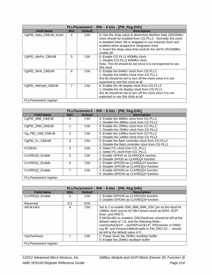
©2012 Advanced Micro Devices, Inc. SMBus Module and ACPI Block (Device 20, Function 0) AMD SP5100 Register Reference Guide Page 214
PLLParameter2 – RW – 8 bits - [PM_Reg:D2h] Field Name Bits Default Description
CgPll2_Sata_ClkEnB_Invert 4 1’b0 0: Use the strap value to determine whether Sata 100/25Mhz clock should be enabled from CG PLL2. Normally this clock is disabled when SB is strapped to use external clock and enabled when strapped to integrated clock. 1: Invert the strap value that controls the SATA 25/100Mhz enable bit
CgPll2_IdePci_ClkEnB 5 1’b0 0: Enable CG PLL2 400Mhz clock 1: Disable CG PLL2 400Mhz clock Note: This bit should be set since it is not expected to use this clock
CgPll2_Alink_ClkEnB 6 1’b0 0: Enable the 64Mhz clock from CG PLL2 1: Disable the 64Mhz clock from CG PLL2 this bit should be set to turn off the clock since it is not expected to use this clock at all
CgPll2_NbDspll_ClkEnB 7 1’b0 0: Enable the nb display clock from CG PLL2 1: Disable the nb display clock from CG PLL2 this bit should be set to turn off the clock since it is not expected to use this clock at all
PLLParameter2 register
PLLParameter3 – RW – 8 bits - [PM_Reg:D3h] Field Name Bits Default Description
CgPll2_48M_ClkEnB 0 1’b0 0: Enable the 48Mhz clock from CG PLL2 1: Disable the 48Mhz clock from CG PLL2
CgPll2_25M_ClkEnB 1 1’b0 0: Enable the 25Mhz clock from CG PLL2 1: Disable the 25Mhz clock from CG PLL2
Cg_Pll2_14M_ClkEnB 2 1’b0 0: Enable the 14Mhz clock from CG PLL2 1: Disable the 14Mhz clock from CG PLL2
CgPll2_Fc_ClkEnB 3 1’b0 0: Enable the flash controller clock from CG PLL2 1: Disable the flash controller clock from CG PLL2
FcClkSrc 4 1’b0 0: Select FC clock from CG_PLL1 1: Select FC clock from CG_PLL2
CLKREQ0_Enable 5 1’b0 1: Enable GPIO0 as CLKREQ0# function 0: Disable GPIO0 as CLKREQ# function
CLKREQ1_Enable 6 1’b0 1: Enable GPIO39 as CLKREQ1# function 0: Disable GPIO39 as CLKREQ1# function
CLKREQ2_Enable 7 1’b0 1: Enable GPIO40 as CLKREQ2# function 0: Disable GPIO40 as CLKREQ2# function
PLLParameter3 register
PLLParameter4 – RW – 8 bits - [PM_Reg:D4h] Field Name Bits Default Description
CLKREQ3_Enable 0 1’b0 1: Enable GPIO40 as CLKREQ3# function 0: Disable GPIO40 as CLKREQ3# function
Reserved 5:1 5’h0 AltClk14En 6 1’b0 Set to 1 to enable 25M_48M_66M_OSC pin as the input for
14MHz clock source for SB’s timers (such as 8254, ACPI timer, and HPET). If AltClk14En is enabled, OSCPwrDown should be left at the default value of ‘1’b, and the following fields -- UseOscAsClk14* , UsePll2ForClk14*, Pll2UseOsc in PMIO reg 9F, and Precise14MhzEnable in PM_REG 53 -- should be left at the default value of 0.
OscPwrDown 7 1’b0 1: Power down the 25Mhz oscillator buffer 0: Enable the 25Mhz oscillator buffer
PLLParameter4 register
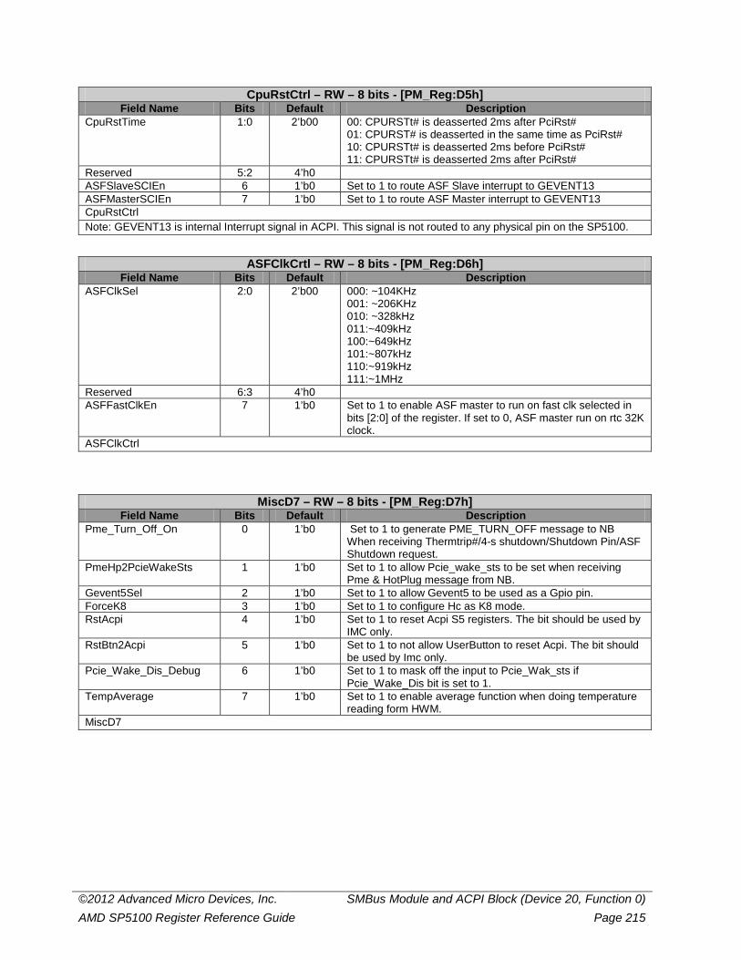
©2012 Advanced Micro Devices, Inc. SMBus Module and ACPI Block (Device 20, Function 0) AMD SP5100 Register Reference Guide Page 215
CpuRstCtrl – RW – 8 bits - [PM_Reg:D5h] Field Name Bits Default Description
CpuRstTime 1:0 2’b00 00: CPURSTt# is deasserted 2ms after PciRst# 01: CPURST# is deasserted in the same time as PciRst# 10: CPURSTt# is deasserted 2ms before PciRst# 11: CPURSTt# is deasserted 2ms after PciRst#
Reserved 5:2 4’h0 ASFSlaveSCIEn 6 1’b0 Set to 1 to route ASF Slave interrupt to GEVENT13 ASFMasterSCIEn 7 1’b0 Set to 1 to route ASF Master interrupt to GEVENT13 CpuRstCtrl Note: GEVENT13 is internal Interrupt signal in ACPI. This signal is not routed to any physical pin on the SP5100.
ASFClkCrtl – RW – 8 bits - [PM_Reg:D6h] Field Name Bits Default Description
ASFClkSel 2:0 2’b00 000: ~104KHz 001: ~206KHz 010: ~328kHz 011:~409kHz 100:~649kHz 101:~807kHz 110:~919kHz 111:~1MHz
Reserved 6:3 4’h0 ASFFastClkEn 7 1’b0 Set to 1 to enable ASF master to run on fast clk selected in
bits [2:0] of the register. If set to 0, ASF master run on rtc 32K clock.
ASFClkCtrl
MiscD7 – RW – 8 bits - [PM_Reg:D7h] Field Name Bits Default Description
Pme_Turn_Off_On 0 1’b0 Set to 1 to generate PME_TURN_OFF message to NB When receiving Thermtrip#/4-s shutdown/Shutdown Pin/ASF Shutdown request.
PmeHp2PcieWakeSts 1 1’b0 Set to 1 to allow Pcie_wake_sts to be set when receiving Pme & HotPlug message from NB.
Gevent5Sel 2 1’b0 Set to 1 to allow Gevent5 to be used as a Gpio pin. ForceK8 3 1’b0 Set to 1 to configure Hc as K8 mode. RstAcpi 4 1’b0 Set to 1 to reset Acpi S5 registers. The bit should be used by
IMC only. RstBtn2Acpi 5 1’b0 Set to 1 to not allow UserButton to reset Acpi. The bit should
be used by Imc only. Pcie_Wake_Dis_Debug 6 1’b0 Set to 1 to mask off the input to Pcie_Wak_sts if
Pcie_Wake_Dis bit is set to 1. TempAverage 7 1’b0 Set to 1 to enable average function when doing temperature
reading form HWM. MiscD7
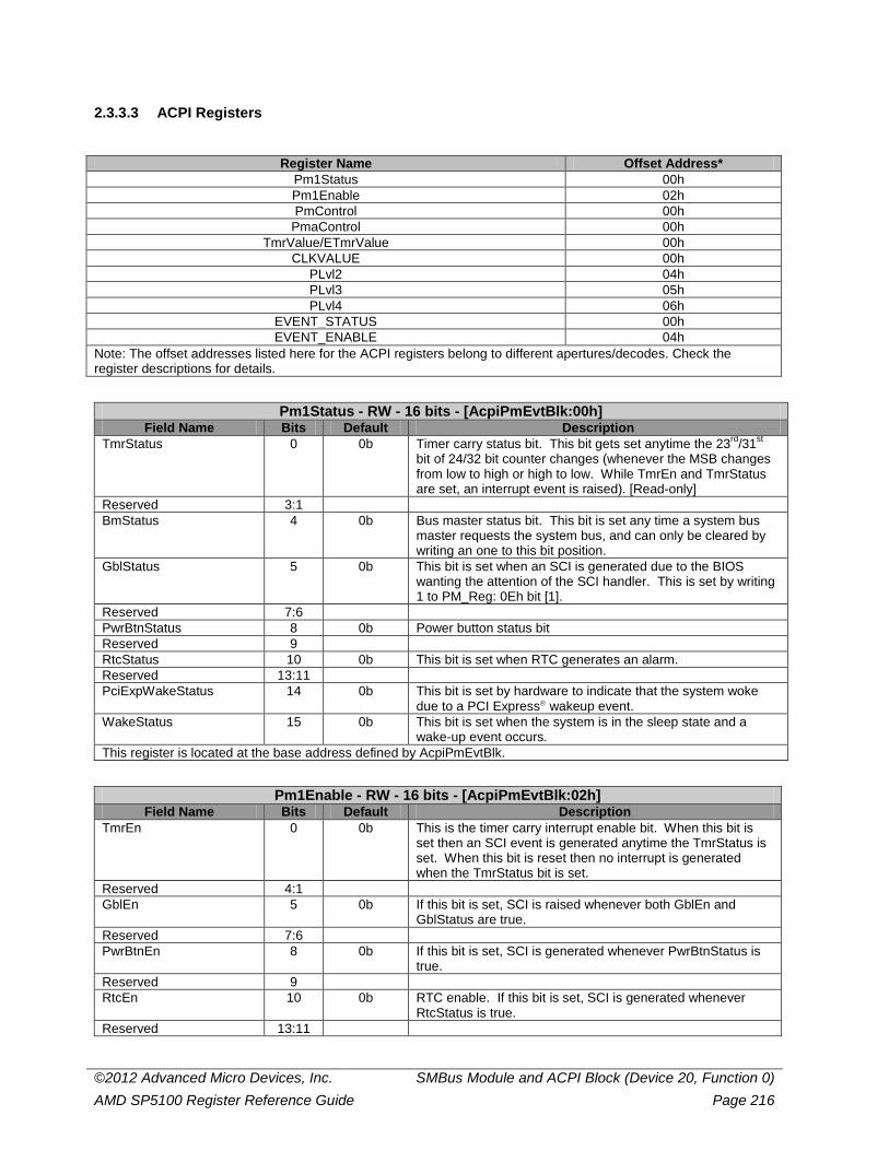
©2012 Advanced Micro Devices, Inc. SMBus Module and ACPI Block (Device 20, Function 0) AMD SP5100 Register Reference Guide Page 216
2.3.3.3 ACPI Registers
Register Name Offset Address* Pm1Status 00h Pm1Enable 02h PmControl 00h
PmaControl 00h TmrValue/ETmrValue 00h
CLKVALUE 00h PLvl2 04h PLvl3 05h PLvl4 06h
EVENT_STATUS 00h EVENT_ENABLE 04h
Note: The offset addresses listed here for the ACPI registers belong to different apertures/decodes. Check the register descriptions for details.
Pm1Status - RW - 16 bits - [AcpiPmEvtBlk:00h] Field Name Bits Default Description
TmrStatus 0 0b Timer carry status bit. This bit gets set anytime the 23rd/31st bit of 24/32 bit counter changes (whenever the MSB changes from low to high or high to low. While TmrEn and TmrStatus are set, an interrupt event is raised). [Read-only]
Reserved 3:1 BmStatus 4 0b Bus master status bit. This bit is set any time a system bus
master requests the system bus, and can only be cleared by writing an one to this bit position.
GblStatus 5 0b This bit is set when an SCI is generated due to the BIOS wanting the attention of the SCI handler. This is set by writing 1 to PM_Reg: 0Eh bit [1].
Reserved 7:6 PwrBtnStatus 8 0b Power button status bit Reserved 9 RtcStatus 10 0b This bit is set when RTC generates an alarm. Reserved 13:11 PciExpWakeStatus 14 0b This bit is set by hardware to indicate that the system woke
due to a PCI Express wakeup event. WakeStatus 15 0b This bit is set when the system is in the sleep state and a
wake-up event occurs. This register is located at the base address defined by AcpiPmEvtBlk.
Pm1Enable - RW - 16 bits - [AcpiPmEvtBlk:02h] Field Name Bits Default Description
TmrEn 0 0b This is the timer carry interrupt enable bit. When this bit is set then an SCI event is generated anytime the TmrStatus is set. When this bit is reset then no interrupt is generated when the TmrStatus bit is set.
Reserved 4:1 GblEn 5 0b If this bit is set, SCI is raised whenever both GblEn and
GblStatus are true. Reserved 7:6 PwrBtnEn 8 0b If this bit is set, SCI is generated whenever PwrBtnStatus is
true. Reserved 9 RtcEn 10 0b RTC enable. If this bit is set, SCI is generated whenever
RtcStatus is true. Reserved 13:11
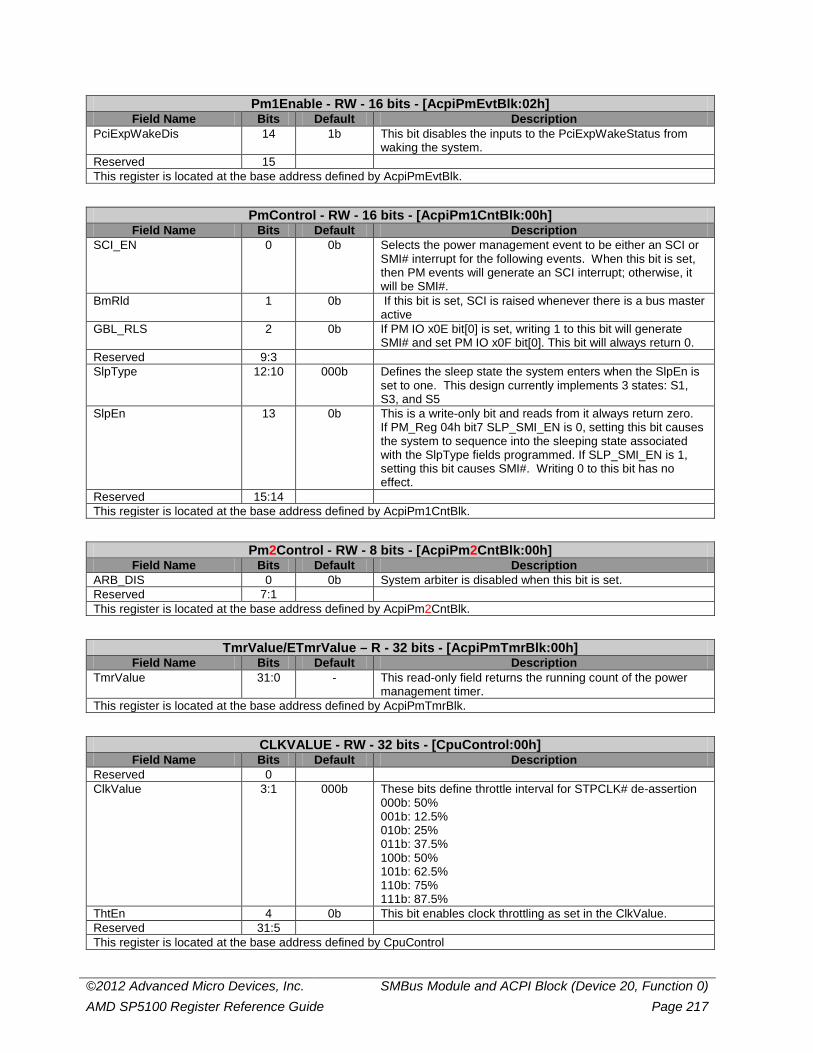
©2012 Advanced Micro Devices, Inc. SMBus Module and ACPI Block (Device 20, Function 0) AMD SP5100 Register Reference Guide Page 217
Pm1Enable - RW - 16 bits - [AcpiPmEvtBlk:02h] Field Name Bits Default Description
PciExpWakeDis 14 1b This bit disables the inputs to the PciExpWakeStatus from waking the system.
Reserved 15 This register is located at the base address defined by AcpiPmEvtBlk.
PmControl - RW - 16 bits - [AcpiPm1CntBlk:00h] Field Name Bits Default Description
SCI_EN 0 0b Selects the power management event to be either an SCI or SMI# interrupt for the following events. When this bit is set, then PM events will generate an SCI interrupt; otherwise, it will be SMI#.
BmRld 1 0b If this bit is set, SCI is raised whenever there is a bus master active
GBL_RLS 2 0b If PM IO x0E bit[0] is set, writing 1 to this bit will generate SMI# and set PM IO x0F bit[0]. This bit will always return 0.
Reserved 9:3 SlpType 12:10 000b Defines the sleep state the system enters when the SlpEn is
set to one. This design currently implements 3 states: S1, S3, and S5
SlpEn 13 0b This is a write-only bit and reads from it always return zero. If PM_Reg 04h bit7 SLP_SMI_EN is 0, setting this bit causes the system to sequence into the sleeping state associated with the SlpType fields programmed. If SLP_SMI_EN is 1, setting this bit causes SMI#. Writing 0 to this bit has no effect.
Reserved 15:14 This register is located at the base address defined by AcpiPm1CntBlk.
Pm2Control - RW - 8 bits - [AcpiPm2CntBlk:00h] Field Name Bits Default Description
ARB_DIS 0 0b System arbiter is disabled when this bit is set. Reserved 7:1 This register is located at the base address defined by AcpiPm2CntBlk.
TmrValue/ETmrValue – R - 32 bits - [AcpiPmTmrBlk:00h] Field Name Bits Default Description
TmrValue 31:0 - This read-only field returns the running count of the power management timer.
This register is located at the base address defined by AcpiPmTmrBlk.
CLKVALUE - RW - 32 bits - [CpuControl:00h] Field Name Bits Default Description
Reserved 0 ClkValue 3:1 000b These bits define throttle interval for STPCLK# de-assertion
000b: 50% 001b: 12.5% 010b: 25% 011b: 37.5% 100b: 50% 101b: 62.5% 110b: 75% 111b: 87.5%
ThtEn 4 0b This bit enables clock throttling as set in the ClkValue. Reserved 31:5 This register is located at the base address defined by CpuControl
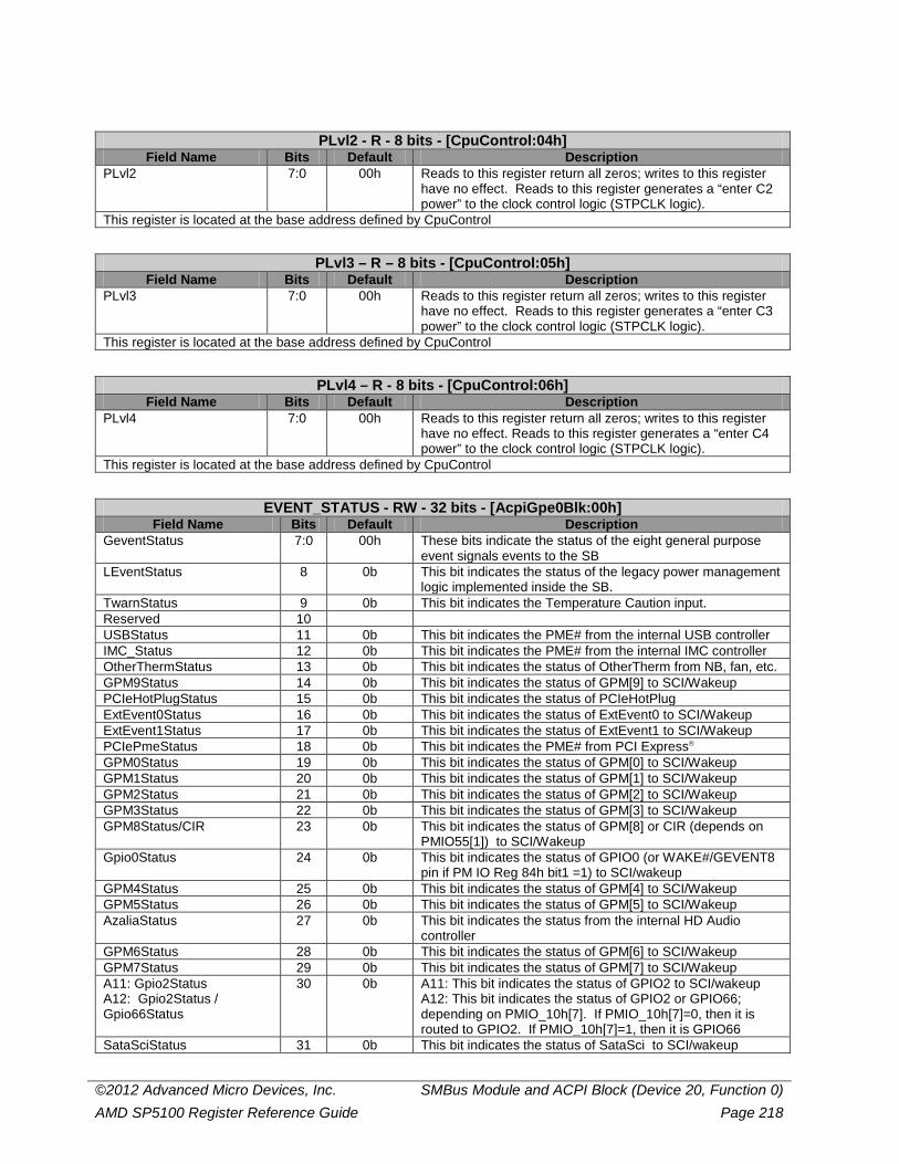
©2012 Advanced Micro Devices, Inc. SMBus Module and ACPI Block (Device 20, Function 0) AMD SP5100 Register Reference Guide Page 218
PLvl2 - R - 8 bits - [CpuControl:04h] Field Name Bits Default Description
PLvl2 7:0 00h Reads to this register return all zeros; writes to this register have no effect. Reads to this register generates a “enter C2 power” to the clock control logic (STPCLK logic).
This register is located at the base address defined by CpuControl
PLvl3 – R – 8 bits - [CpuControl:05h] Field Name Bits Default Description
PLvl3 7:0 00h Reads to this register return all zeros; writes to this register have no effect. Reads to this register generates a “enter C3 power” to the clock control logic (STPCLK logic).
This register is located at the base address defined by CpuControl
PLvl4 – R - 8 bits - [CpuControl:06h] Field Name Bits Default Description
PLvl4 7:0 00h Reads to this register return all zeros; writes to this register have no effect. Reads to this register generates a “enter C4 power” to the clock control logic (STPCLK logic).
This register is located at the base address defined by CpuControl
EVENT_STATUS - RW - 32 bits - [AcpiGpe0Blk:00h] Field Name Bits Default Description
GeventStatus 7:0 00h These bits indicate the status of the eight general purpose event signals events to the SB
LEventStatus 8 0b This bit indicates the status of the legacy power management logic implemented inside the SB.
TwarnStatus 9 0b This bit indicates the Temperature Caution input. Reserved 10 USBStatus 11 0b This bit indicates the PME# from the internal USB controller IMC_Status 12 0b This bit indicates the PME# from the internal IMC controller OtherThermStatus 13 0b This bit indicates the status of OtherTherm from NB, fan, etc. GPM9Status 14 0b This bit indicates the status of GPM[9] to SCI/Wakeup PCIeHotPlugStatus 15 0b This bit indicates the status of PCIeHotPlug ExtEvent0Status 16 0b This bit indicates the status of ExtEvent0 to SCI/Wakeup ExtEvent1Status 17 0b This bit indicates the status of ExtEvent1 to SCI/Wakeup PCIePmeStatus 18 0b This bit indicates the PME# from PCI Express GPM0Status 19 0b This bit indicates the status of GPM[0] to SCI/Wakeup GPM1Status 20 0b This bit indicates the status of GPM[1] to SCI/Wakeup GPM2Status 21 0b This bit indicates the status of GPM[2] to SCI/Wakeup GPM3Status 22 0b This bit indicates the status of GPM[3] to SCI/Wakeup GPM8Status/CIR 23 0b This bit indicates the status of GPM[8] or CIR (depends on
PMIO55[1]) to SCI/Wakeup Gpio0Status 24 0b This bit indicates the status of GPIO0 (or WAKE#/GEVENT8
pin if PM IO Reg 84h bit1 =1) to SCI/wakeup GPM4Status 25 0b This bit indicates the status of GPM[4] to SCI/Wakeup GPM5Status 26 0b This bit indicates the status of GPM[5] to SCI/Wakeup AzaliaStatus 27 0b This bit indicates the status from the internal HD Audio
controller GPM6Status 28 0b This bit indicates the status of GPM[6] to SCI/Wakeup GPM7Status 29 0b This bit indicates the status of GPM[7] to SCI/Wakeup A11: Gpio2Status A12: Gpio2Status / Gpio66Status
30 0b A11: This bit indicates the status of GPIO2 to SCI/wakeup A12: This bit indicates the status of GPIO2 or GPIO66; depending on PMIO_10h[7]. If PMIO_10h[7]=0, then it is routed to GPIO2. If PMIO_10h[7]=1, then it is GPIO66
SataSciStatus 31 0b This bit indicates the status of SataSci to SCI/wakeup
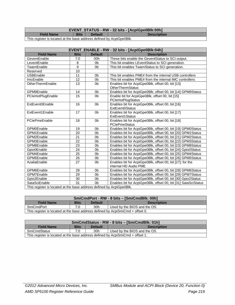
©2012 Advanced Micro Devices, Inc. SMBus Module and ACPI Block (Device 20, Function 0) AMD SP5100 Register Reference Guide Page 219
EVENT_STATUS - RW - 32 bits - [AcpiGpe0Blk:00h] Field Name Bits Default Description
This register is located at the base address defined by AcpiGpe0Blk.
EVENT_ENABLE - RW - 32 bits - [AcpiGpe0Blk:04h] Field Name Bits Default Description
GeventEnable 7:0 00h These bits enable the GeventStatus to SCI output. LeventEnable 8 0b This bit enables LEventStatus to SCI generation. TwarnEnable 9 0b This bit enables TwarnStatus to SCI generation. Reserved 10 USBEnable 11 0b This bit enables PME# from the internal USB controllers ImcEnable 12 0b This bit enables PME# from the internal IMC controllers OtherThermEnable 13 0b Enables bit for AcpiGpe0Blk, offset 00, bit [13]
OtherThermStatus GPM9Enable 14 0b Enables bit for AcpiGpe0Blk, offset 00, bit [14] GPM9Status PCIeHotPlugEnable 15 0b Enable bit for AcpiGpe0Blk, offset 00, bit [15]
PCIeHotPlugStatus ExtEvent0Enable 16 0b Enables bit for AcpiGpe0Blk, offset 00, bit [16]
ExtEvent0Status ExtEvent1Enable 17 0b Enables bit for AcpiGpe0Blk, offset 00, bit [17]
ExtEvent1Status PCIePmeEnable 18 0b Enables bit for AcpiGpe0Blk, offset 00, bit [18]
PCIePmeStatus GPM0Enable 19 0b Enables bit for AcpiGpe0Blk, offset 00, bit [19] GPM0Status GPM1Enable 20 0b Enables bit for AcpiGpe0Blk, offset 00, bit [20] GPM1Status GPM2Enable 21 0b Enables bit for AcpiGpe0Blk, offset 00, bit [21] GPM2Status GPM3Enable 22 0b Enables bit for AcpiGpe0Blk, offset 00, bit [22] GPM3Status GPM8Enable 23 0b Enables bit for AcpiGpe0Blk, offset 00, bit [23] GPM8Status Gpio0Enable 24 0b Enables bit for AcpiGpe0Blk, offset 00, bit [24] Gpio0Status GPM4Enable 25 0b Enables bit for AcpiGpe0Blk, offset 00, bit [25] GPM4Status GPM5Enable 26 0b Enables bit for AcpiGpe0Blk, offset 00, bit [26] GPM5Status AzaliaEnable 27 0b Enables bit for AcpiGpe0Blk, offset 00, bit [27]; for the
internal HD Audio PME GPM6Enable 28 0b Enables bit for AcpiGpe0Blk, offset 00, bit [28] GPM6Status GPM7Enable 29 0b Enables bit for AcpiGpe0Blk, offset 00, bit [29] GPM7Status Gpio2Enable 30 0b Enables bit for AcpiGpe0Blk, offset 00, bit [30] Gpio2Status SataSciEnable 31 0b Enables bit for AcpiGpe0Blk, offset 00, bit [31] SataSciStatus This register is located at the base address defined by AcpiGpe0Blk.
SmiCmdPort - RW - 8 bits – [SmiCmdBlk: 00h] Field Name Bits Default Description
SmiCmdPort 7:0 00h Used by the BIOS and the OS This register is located at the base address defined by AcpiSmiCmd + offset 0.
SmiCmdStatus - RW - 8 bits – [SmiCmdBlk: 01h] Field Name Bits Default Description
SmiCmdStatus 7:0 00h Used by the BIOS and the OS This register is located at the base address defined by AcpiSmiCmd + offset 1.
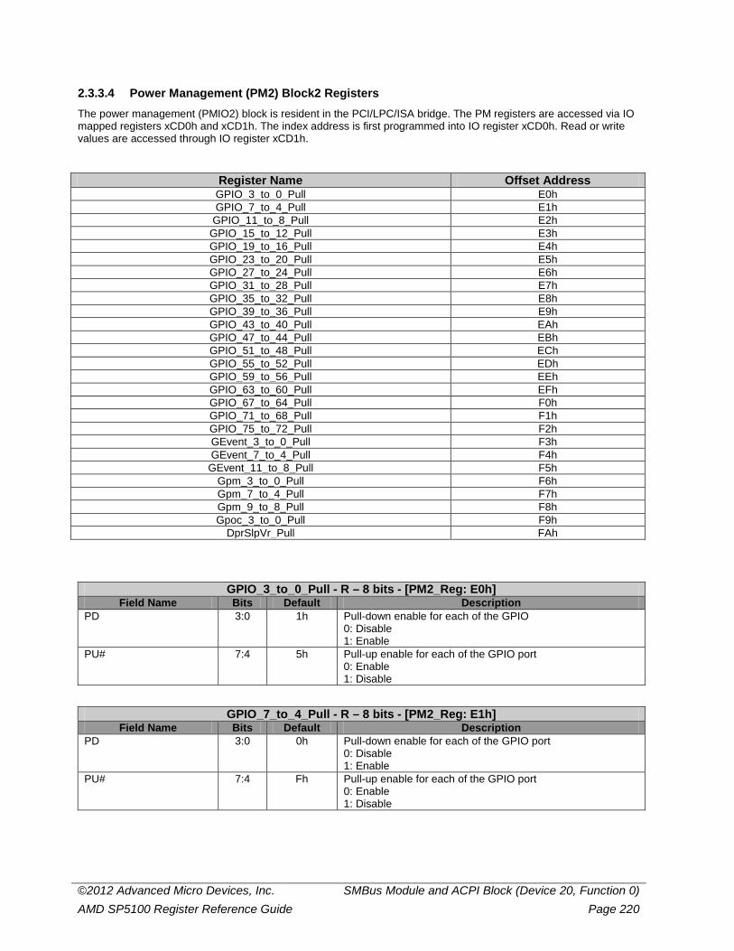
©2012 Advanced Micro Devices, Inc. SMBus Module and ACPI Block (Device 20, Function 0) AMD SP5100 Register Reference Guide Page 220
2.3.3.4 Power Management (PM2) Block2 Registers The power management (PMIO2) block is resident in the PCI/LPC/ISA bridge. The PM registers are accessed via IO mapped registers xCD0h and xCD1h. The index address is first programmed into IO register xCD0h. Read or write values are accessed through IO register xCD1h.
Register Name Offset Address GPIO_3_to_0_Pull E0h GPIO_7_to_4_Pull E1h
GPIO_11_to_8_Pull E2h GPIO_15_to_12_Pull E3h GPIO_19_to_16_Pull E4h GPIO_23_to_20_Pull E5h GPIO_27_to_24_Pull E6h GPIO_31_to_28_Pull E7h GPIO_35_to_32_Pull E8h GPIO_39_to_36_Pull E9h GPIO_43_to_40_Pull EAh GPIO_47_to_44_Pull EBh GPIO_51_to_48_Pull ECh GPIO_55_to_52_Pull EDh GPIO_59_to_56_Pull EEh GPIO_63_to_60_Pull EFh GPIO_67_to_64_Pull F0h GPIO_71_to_68_Pull F1h GPIO_75_to_72_Pull F2h GEvent_3_to_0_Pull F3h GEvent_7_to_4_Pull F4h
GEvent_11_to_8_Pull F5h Gpm_3_to_0_Pull F6h Gpm_7_to_4_Pull F7h Gpm_9_to_8_Pull F8h Gpoc_3_to_0_Pull F9h
DprSlpVr_Pull FAh
GPIO_3_to_0_Pull - R – 8 bits - [PM2_Reg: E0h] Field Name Bits Default Description
PD 3:0 1h Pull-down enable for each of the GPIO 0: Disable 1: Enable
PU# 7:4 5h Pull-up enable for each of the GPIO port 0: Enable 1: Disable
GPIO_7_to_4_Pull - R – 8 bits - [PM2_Reg: E1h] Field Name Bits Default Description
PD 3:0 0h Pull-down enable for each of the GPIO port 0: Disable 1: Enable
PU# 7:4 Fh Pull-up enable for each of the GPIO port 0: Enable 1: Disable
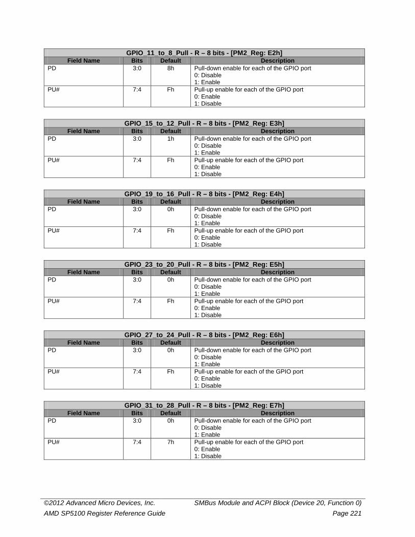
©2012 Advanced Micro Devices, Inc. SMBus Module and ACPI Block (Device 20, Function 0) AMD SP5100 Register Reference Guide Page 221
GPIO_11_to_8_Pull - R – 8 bits - [PM2_Reg: E2h] Field Name Bits Default Description
PD 3:0 8h Pull-down enable for each of the GPIO port 0: Disable 1: Enable
PU# 7:4 Fh Pull-up enable for each of the GPIO port 0: Enable 1: Disable
GPIO_15_to_12_Pull - R – 8 bits - [PM2_Reg: E3h] Field Name Bits Default Description
PD 3:0 1h Pull-down enable for each of the GPIO port 0: Disable 1: Enable
PU# 7:4 Fh Pull-up enable for each of the GPIO port 0: Enable 1: Disable
GPIO_19_to_16_Pull - R – 8 bits - [PM2_Reg: E4h] Field Name Bits Default Description
PD 3:0 0h Pull-down enable for each of the GPIO port 0: Disable 1: Enable
PU# 7:4 Fh Pull-up enable for each of the GPIO port 0: Enable 1: Disable
GPIO_23_to_20_Pull - R – 8 bits - [PM2_Reg: E5h] Field Name Bits Default Description
PD 3:0 0h Pull-down enable for each of the GPIO port 0: Disable 1: Enable
PU# 7:4 Fh Pull-up enable for each of the GPIO port 0: Enable 1: Disable
GPIO_27_to_24_Pull - R – 8 bits - [PM2_Reg: E6h] Field Name Bits Default Description
PD 3:0 0h Pull-down enable for each of the GPIO port 0: Disable 1: Enable
PU# 7:4 Fh Pull-up enable for each of the GPIO port 0: Enable 1: Disable
GPIO_31_to_28_Pull - R – 8 bits - [PM2_Reg: E7h] Field Name Bits Default Description
PD 3:0 0h Pull-down enable for each of the GPIO port 0: Disable 1: Enable
PU# 7:4 7h Pull-up enable for each of the GPIO port 0: Enable 1: Disable
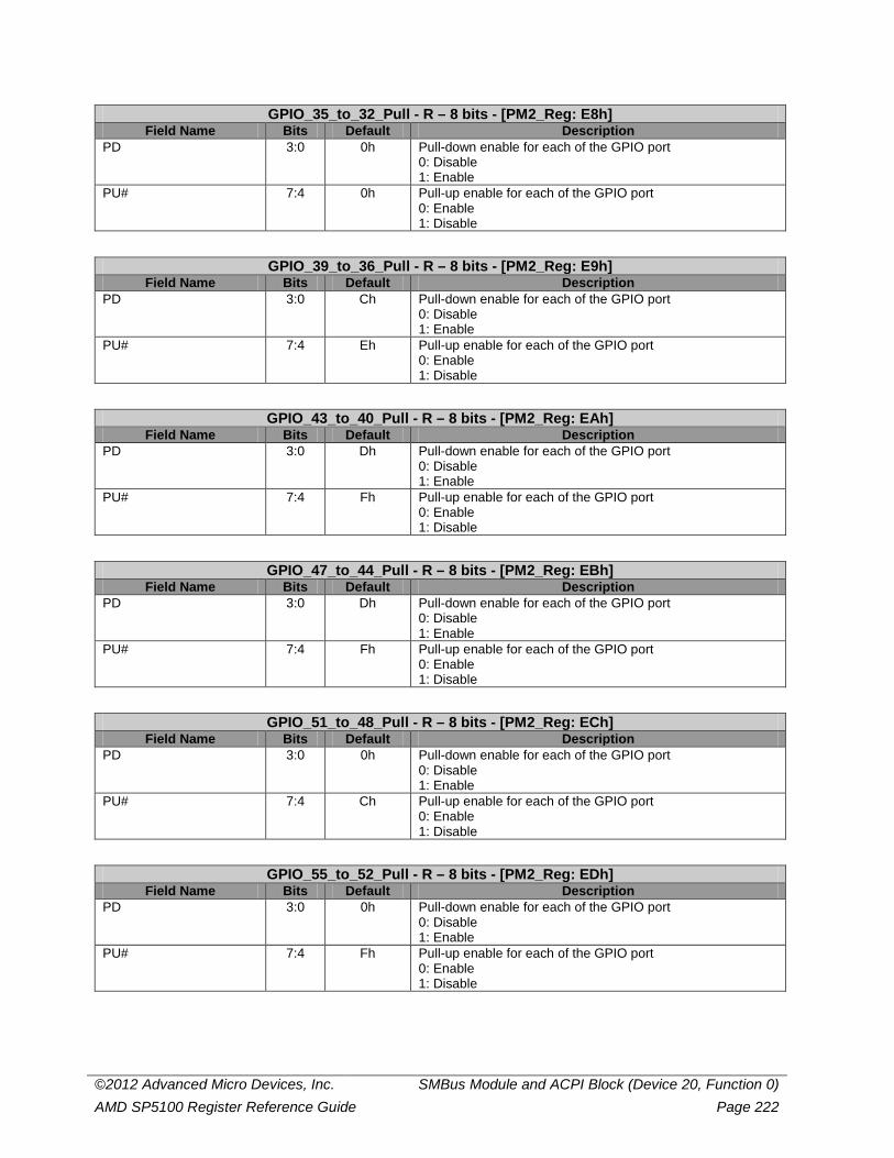
©2012 Advanced Micro Devices, Inc. SMBus Module and ACPI Block (Device 20, Function 0) AMD SP5100 Register Reference Guide Page 222
GPIO_35_to_32_Pull - R – 8 bits - [PM2_Reg: E8h] Field Name Bits Default Description
PD 3:0 0h Pull-down enable for each of the GPIO port 0: Disable 1: Enable
PU# 7:4 0h Pull-up enable for each of the GPIO port 0: Enable 1: Disable
GPIO_39_to_36_Pull - R – 8 bits - [PM2_Reg: E9h] Field Name Bits Default Description
PD 3:0 Ch Pull-down enable for each of the GPIO port 0: Disable 1: Enable
PU# 7:4 Eh Pull-up enable for each of the GPIO port 0: Enable 1: Disable
GPIO_43_to_40_Pull - R – 8 bits - [PM2_Reg: EAh] Field Name Bits Default Description
PD 3:0 Dh Pull-down enable for each of the GPIO port 0: Disable 1: Enable
PU# 7:4 Fh Pull-up enable for each of the GPIO port 0: Enable 1: Disable
GPIO_47_to_44_Pull - R – 8 bits - [PM2_Reg: EBh] Field Name Bits Default Description
PD 3:0 Dh Pull-down enable for each of the GPIO port 0: Disable 1: Enable
PU# 7:4 Fh Pull-up enable for each of the GPIO port 0: Enable 1: Disable
GPIO_51_to_48_Pull - R – 8 bits - [PM2_Reg: ECh] Field Name Bits Default Description
PD 3:0 0h Pull-down enable for each of the GPIO port 0: Disable 1: Enable
PU# 7:4 Ch Pull-up enable for each of the GPIO port 0: Enable 1: Disable
GPIO_55_to_52_Pull - R – 8 bits - [PM2_Reg: EDh] Field Name Bits Default Description
PD 3:0 0h Pull-down enable for each of the GPIO port 0: Disable 1: Enable
PU# 7:4 Fh Pull-up enable for each of the GPIO port 0: Enable 1: Disable
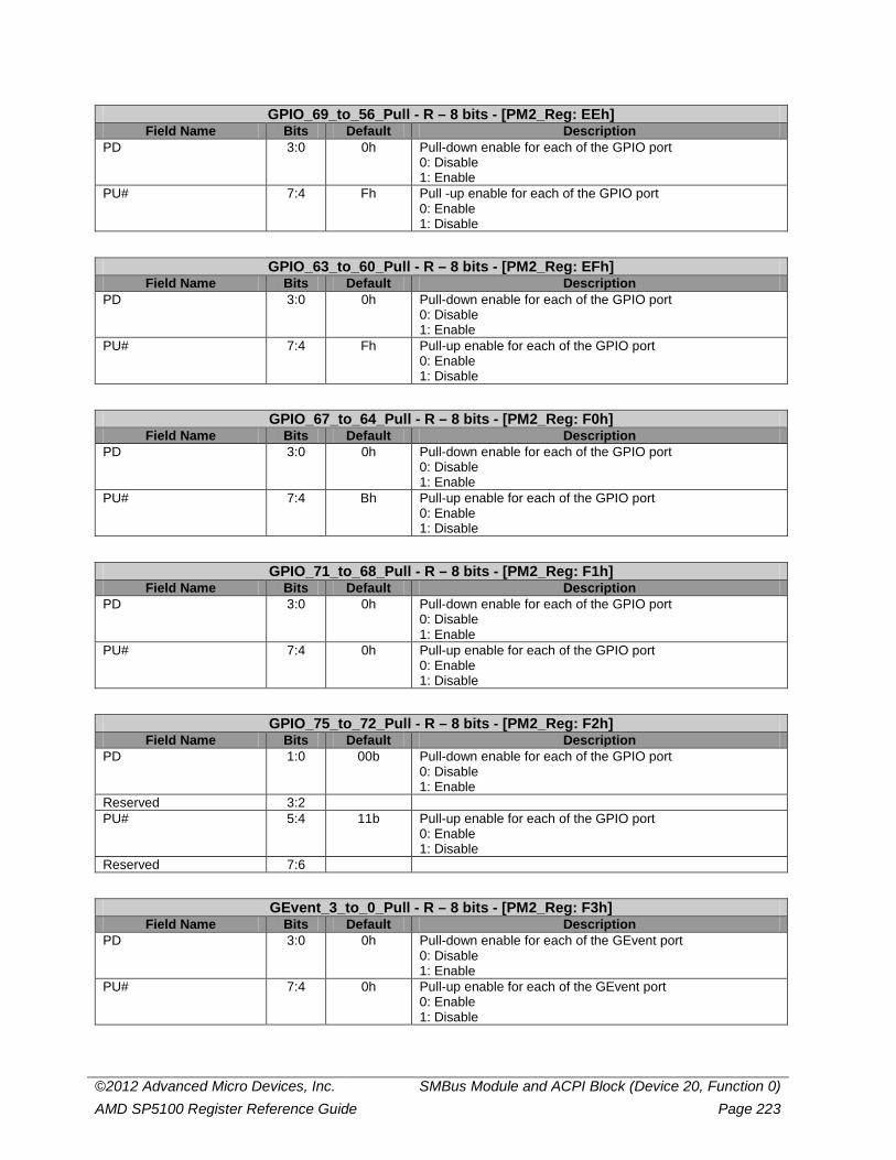
©2012 Advanced Micro Devices, Inc. SMBus Module and ACPI Block (Device 20, Function 0) AMD SP5100 Register Reference Guide Page 223
GPIO_69_to_56_Pull - R – 8 bits - [PM2_Reg: EEh] Field Name Bits Default Description
PD 3:0 0h Pull-down enable for each of the GPIO port 0: Disable 1: Enable
PU# 7:4 Fh Pull -up enable for each of the GPIO port 0: Enable 1: Disable
GPIO_63_to_60_Pull - R – 8 bits - [PM2_Reg: EFh] Field Name Bits Default Description
PD 3:0 0h Pull-down enable for each of the GPIO port 0: Disable 1: Enable
PU# 7:4 Fh Pull-up enable for each of the GPIO port 0: Enable 1: Disable
GPIO_67_to_64_Pull - R – 8 bits - [PM2_Reg: F0h] Field Name Bits Default Description
PD 3:0 0h Pull-down enable for each of the GPIO port 0: Disable 1: Enable
PU# 7:4 Bh Pull-up enable for each of the GPIO port 0: Enable 1: Disable
GPIO_71_to_68_Pull - R – 8 bits - [PM2_Reg: F1h] Field Name Bits Default Description
PD 3:0 0h Pull-down enable for each of the GPIO port 0: Disable 1: Enable
PU# 7:4 0h Pull-up enable for each of the GPIO port 0: Enable 1: Disable
GPIO_75_to_72_Pull - R – 8 bits - [PM2_Reg: F2h] Field Name Bits Default Description
PD 1:0 00b Pull-down enable for each of the GPIO port 0: Disable 1: Enable
Reserved 3:2 PU# 5:4 11b Pull-up enable for each of the GPIO port
0: Enable 1: Disable
Reserved 7:6
GEvent_3_to_0_Pull - R – 8 bits - [PM2_Reg: F3h] Field Name Bits Default Description
PD 3:0 0h Pull-down enable for each of the GEvent port 0: Disable 1: Enable
PU# 7:4 0h Pull-up enable for each of the GEvent port 0: Enable 1: Disable
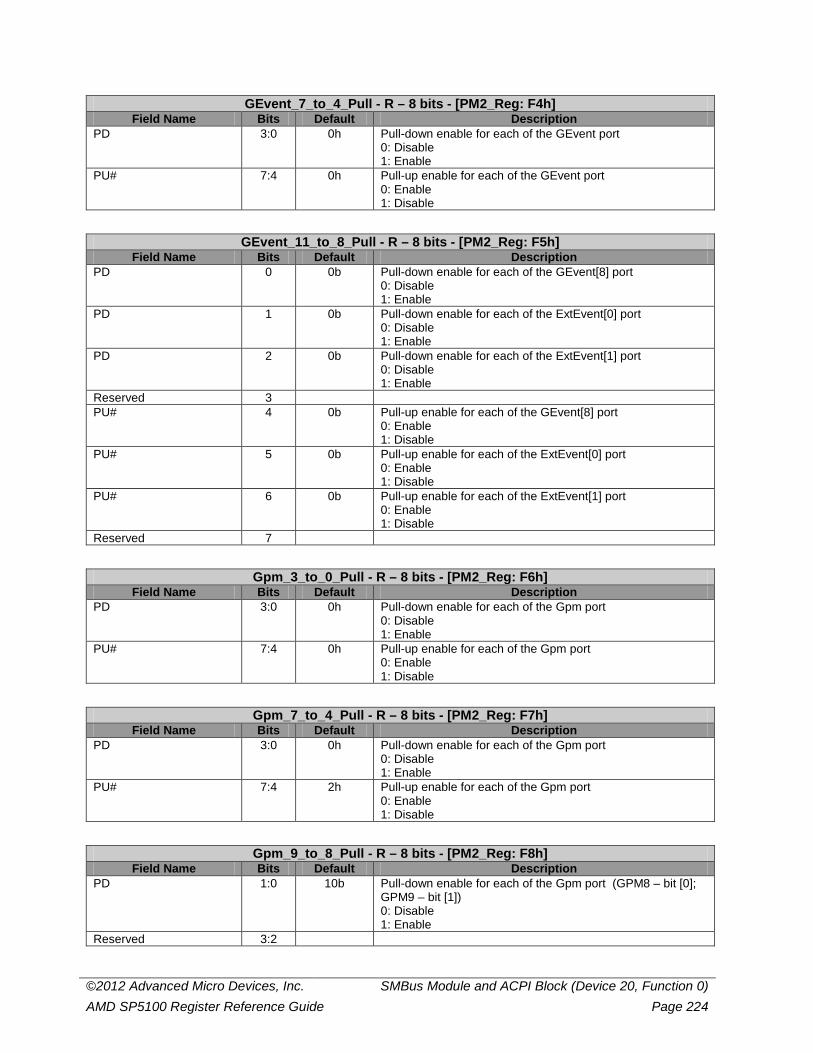
©2012 Advanced Micro Devices, Inc. SMBus Module and ACPI Block (Device 20, Function 0) AMD SP5100 Register Reference Guide Page 224
GEvent_7_to_4_Pull - R – 8 bits - [PM2_Reg: F4h] Field Name Bits Default Description
PD 3:0 0h Pull-down enable for each of the GEvent port 0: Disable 1: Enable
PU# 7:4 0h Pull-up enable for each of the GEvent port 0: Enable 1: Disable
GEvent_11_to_8_Pull - R – 8 bits - [PM2_Reg: F5h] Field Name Bits Default Description
PD 0 0b Pull-down enable for each of the GEvent[8] port 0: Disable 1: Enable
PD 1 0b Pull-down enable for each of the ExtEvent[0] port 0: Disable 1: Enable
PD 2 0b Pull-down enable for each of the ExtEvent[1] port 0: Disable 1: Enable
Reserved 3 PU# 4 0b Pull-up enable for each of the GEvent[8] port
0: Enable 1: Disable
PU# 5 0b Pull-up enable for each of the ExtEvent[0] port 0: Enable 1: Disable
PU# 6 0b Pull-up enable for each of the ExtEvent[1] port 0: Enable 1: Disable
Reserved 7
Gpm_3_to_0_Pull - R – 8 bits - [PM2_Reg: F6h] Field Name Bits Default Description
PD 3:0 0h Pull-down enable for each of the Gpm port 0: Disable 1: Enable
PU# 7:4 0h Pull-up enable for each of the Gpm port 0: Enable 1: Disable
Gpm_7_to_4_Pull - R – 8 bits - [PM2_Reg: F7h] Field Name Bits Default Description
PD 3:0 0h Pull-down enable for each of the Gpm port 0: Disable 1: Enable
PU# 7:4 2h Pull-up enable for each of the Gpm port 0: Enable 1: Disable
Gpm_9_to_8_Pull - R – 8 bits - [PM2_Reg: F8h] Field Name Bits Default Description
PD 1:0 10b Pull-down enable for each of the Gpm port (GPM8 – bit [0]; GPM9 – bit [1]) 0: Disable 1: Enable
Reserved 3:2
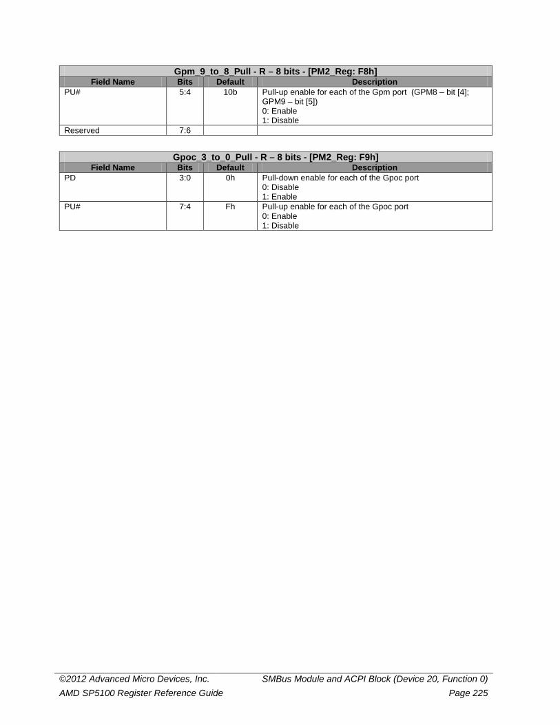
©2012 Advanced Micro Devices, Inc. SMBus Module and ACPI Block (Device 20, Function 0) AMD SP5100 Register Reference Guide Page 225
Gpm_9_to_8_Pull - R – 8 bits - [PM2_Reg: F8h] Field Name Bits Default Description
PU# 5:4 10b Pull-up enable for each of the Gpm port (GPM8 – bit [4]; GPM9 – bit [5]) 0: Enable 1: Disable
Reserved 7:6
Gpoc_3_to_0_Pull - R – 8 bits - [PM2_Reg: F9h] Field Name Bits Default Description
PD 3:0 0h Pull-down enable for each of the Gpoc port 0: Disable 1: Enable
PU# 7:4 Fh Pull-up enable for each of the Gpoc port 0: Enable 1: Disable
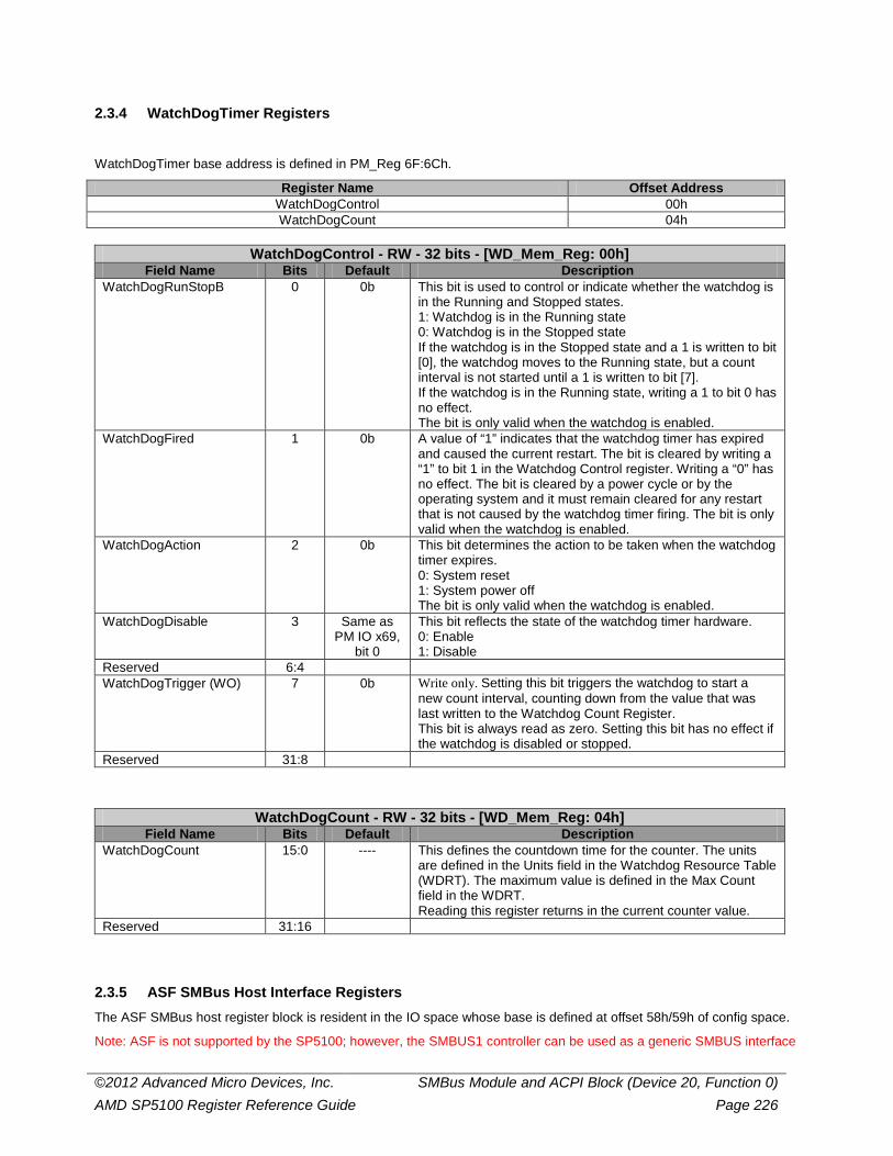
©2012 Advanced Micro Devices, Inc. SMBus Module and ACPI Block (Device 20, Function 0) AMD SP5100 Register Reference Guide Page 226
2.3.4 WatchDogTimer Registers
WatchDogTimer base address is defined in PM_Reg 6F:6Ch.
Register Name Offset Address WatchDogControl 00h WatchDogCount 04h
WatchDogControl - RW - 32 bits - [WD_Mem_Reg: 00h]
Field Name Bits Default Description WatchDogRunStopB 0 0b This bit is used to control or indicate whether the watchdog is
in the Running and Stopped states. 1: Watchdog is in the Running state 0: Watchdog is in the Stopped state If the watchdog is in the Stopped state and a 1 is written to bit [0], the watchdog moves to the Running state, but a count interval is not started until a 1 is written to bit [7]. If the watchdog is in the Running state, writing a 1 to bit 0 has no effect. The bit is only valid when the watchdog is enabled.
WatchDogFired 1 0b A value of “1” indicates that the watchdog timer has expired and caused the current restart. The bit is cleared by writing a “1” to bit 1 in the Watchdog Control register. Writing a “0” has no effect. The bit is cleared by a power cycle or by the operating system and it must remain cleared for any restart that is not caused by the watchdog timer firing. The bit is only valid when the watchdog is enabled.
WatchDogAction 2 0b This bit determines the action to be taken when the watchdog timer expires. 0: System reset 1: System power off The bit is only valid when the watchdog is enabled.
WatchDogDisable 3 Same as PM IO x69,
bit 0
This bit reflects the state of the watchdog timer hardware. 0: Enable 1: Disable
Reserved 6:4 WatchDogTrigger (WO) 7 0b Write only. Setting this bit triggers the watchdog to start a
new count interval, counting down from the value that was last written to the Watchdog Count Register. This bit is always read as zero. Setting this bit has no effect if the watchdog is disabled or stopped.
Reserved 31:8
WatchDogCount - RW - 32 bits - [WD_Mem_Reg: 04h] Field Name Bits Default Description
WatchDogCount 15:0 ---- This defines the countdown time for the counter. The units are defined in the Units field in the Watchdog Resource Table (WDRT). The maximum value is defined in the Max Count field in the WDRT. Reading this register returns in the current counter value.
Reserved 31:16
2.3.5 ASF SMBus Host Interface Registers The ASF SMBus host register block is resident in the IO space whose base is defined at offset 58h/59h of config space.
Note: ASF is not supported by the SP5100; however, the SMBUS1 controller can be used as a generic SMBUS interface
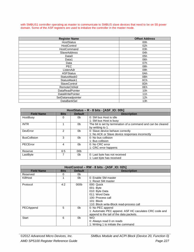
©2012 Advanced Micro Devices, Inc. SMBus Module and ACPI Block (Device 20, Function 0) AMD SP5100 Register Reference Guide Page 227
with SMBUS1 controller operating as master to communicate to SMBUS slave devices that need to be on S5 power domain. Some of the ASF registers are used to initialize the controller in the master mode.
Register Name Offset Address HostStatus 00h HostControl 02h
HostCommand 03h SlaveAddress 04h
Data0 05h Data1 06h Data 07h PEC 08h
ListenAdr 09h ASFStatus 0Ah
StatusMask0 0Bh StatusMask1 0Ch SlaveControl 0Dh
RemoteCtrlAdr 0Eh DataReadPointer 10h DataWritePointer 11h
SetDatareadpointer 12h DataBankSel 13h
HostStatus – R - 8 bits - [ASF_IO: 00h] Field Name Bits Default Description
HostBusy 0 0b 0: SM bus Host is idle 1: SM bus Host is busy
INTR 1 0b The bit is set by termination of a command and can be cleared by writting to 1.
DevError 2 0b 0: Slave device behave correctly 1: No ACK or Slave device responses incorrectly
BusCollision 3 0b 0: No bus collision 1: Bus collision
PECError 4 0b 0: No CRC error 1: CRC error happens
Reserve 6:5 00b LastByte 7 0b 0: Last byte has not received
1: Last byte has received
HostControl – RW - 8 bits - [ASF_IO: 02h] Field Name Bits Default Description
Reserved 0 0b KillHost 1 0b 0: Enable SM master
1: Reset SM master Protocol 4:2 000b 000: Quick
001: Byte 010: Byte Data 011: Word Data 100: Process call 101: Block 110: Block write-Block read-process call
PECAppend 5 0b 0: No PEC append 1: Automatic PEC append. ASF HC caculates CRC code and append to the tail of the data packets.
Start 6 0b WO: 0: Always read 0 on reads 1: Writing 1 to initiate the command
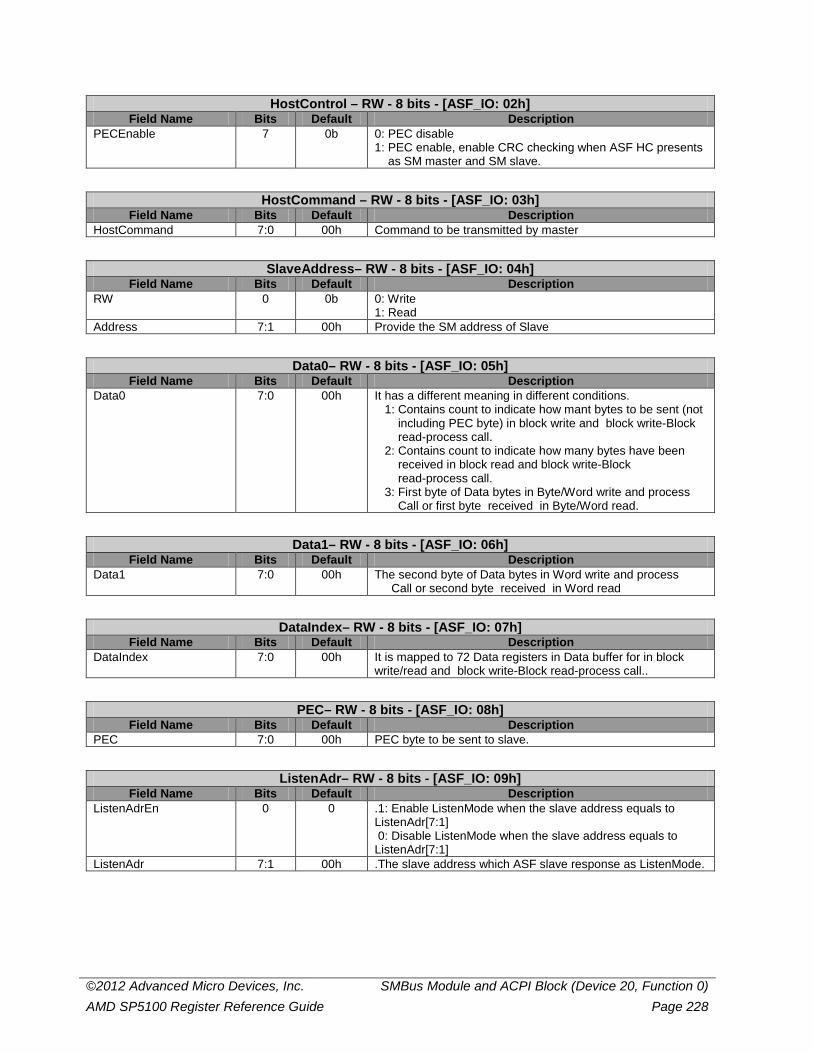
©2012 Advanced Micro Devices, Inc. SMBus Module and ACPI Block (Device 20, Function 0) AMD SP5100 Register Reference Guide Page 228
HostControl – RW - 8 bits - [ASF_IO: 02h] Field Name Bits Default Description
PECEnable 7 0b 0: PEC disable 1: PEC enable, enable CRC checking when ASF HC presents as SM master and SM slave.
HostCommand – RW - 8 bits - [ASF_IO: 03h] Field Name Bits Default Description
HostCommand 7:0 00h Command to be transmitted by master
SlaveAddress– RW - 8 bits - [ASF_IO: 04h] Field Name Bits Default Description
RW 0 0b 0: Write 1: Read
Address 7:1 00h Provide the SM address of Slave
Data0– RW - 8 bits - [ASF_IO: 05h] Field Name Bits Default Description
Data0 7:0 00h It has a different meaning in different conditions. 1: Contains count to indicate how mant bytes to be sent (not including PEC byte) in block write and block write-Block read-process call. 2: Contains count to indicate how many bytes have been received in block read and block write-Block read-process call. 3: First byte of Data bytes in Byte/Word write and process Call or first byte received in Byte/Word read.
Data1– RW - 8 bits - [ASF_IO: 06h] Field Name Bits Default Description
Data1 7:0 00h The second byte of Data bytes in Word write and process Call or second byte received in Word read
DataIndex– RW - 8 bits - [ASF_IO: 07h] Field Name Bits Default Description
DataIndex 7:0 00h It is mapped to 72 Data registers in Data buffer for in block write/read and block write-Block read-process call..
PEC– RW - 8 bits - [ASF_IO: 08h] Field Name Bits Default Description
PEC 7:0 00h PEC byte to be sent to slave.
ListenAdr– RW - 8 bits - [ASF_IO: 09h] Field Name Bits Default Description
ListenAdrEn 0 0 .1: Enable ListenMode when the slave address equals to ListenAdr[7:1] 0: Disable ListenMode when the slave address equals to ListenAdr[7:1]
ListenAdr 7:1 00h .The slave address which ASF slave response as ListenMode.
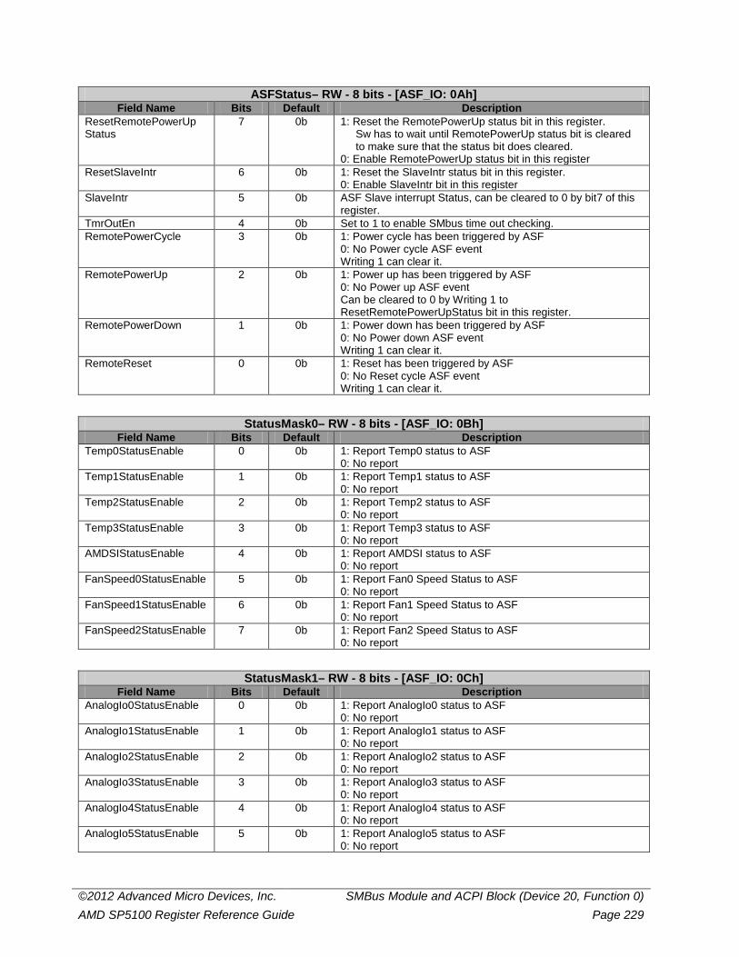
©2012 Advanced Micro Devices, Inc. SMBus Module and ACPI Block (Device 20, Function 0) AMD SP5100 Register Reference Guide Page 229
ASFStatus– RW - 8 bits - [ASF_IO: 0Ah] Field Name Bits Default Description
ResetRemotePowerUp Status
7 0b 1: Reset the RemotePowerUp status bit in this register. Sw has to wait until RemotePowerUp status bit is cleared to make sure that the status bit does cleared. 0: Enable RemotePowerUp status bit in this register
ResetSlaveIntr 6 0b 1: Reset the SlaveIntr status bit in this register. 0: Enable SlaveIntr bit in this register
SlaveIntr 5 0b ASF Slave interrupt Status, can be cleared to 0 by bit7 of this register.
TmrOutEn 4 0b Set to 1 to enable SMbus time out checking. RemotePowerCycle 3 0b 1: Power cycle has been triggered by ASF
0: No Power cycle ASF event Writing 1 can clear it.
RemotePowerUp 2 0b 1: Power up has been triggered by ASF 0: No Power up ASF event Can be cleared to 0 by Writing 1 to ResetRemotePowerUpStatus bit in this register.
RemotePowerDown 1 0b 1: Power down has been triggered by ASF 0: No Power down ASF event Writing 1 can clear it.
RemoteReset 0 0b 1: Reset has been triggered by ASF 0: No Reset cycle ASF event Writing 1 can clear it.
StatusMask0– RW - 8 bits - [ASF_IO: 0Bh] Field Name Bits Default Description
Temp0StatusEnable 0 0b 1: Report Temp0 status to ASF 0: No report
Temp1StatusEnable 1 0b 1: Report Temp1 status to ASF 0: No report
Temp2StatusEnable 2 0b 1: Report Temp2 status to ASF 0: No report
Temp3StatusEnable 3 0b 1: Report Temp3 status to ASF 0: No report
AMDSIStatusEnable 4 0b 1: Report AMDSI status to ASF 0: No report
FanSpeed0StatusEnable 5 0b 1: Report Fan0 Speed Status to ASF 0: No report
FanSpeed1StatusEnable 6 0b 1: Report Fan1 Speed Status to ASF 0: No report
FanSpeed2StatusEnable 7 0b 1: Report Fan2 Speed Status to ASF 0: No report
StatusMask1– RW - 8 bits - [ASF_IO: 0Ch] Field Name Bits Default Description
AnalogIo0StatusEnable 0 0b 1: Report AnalogIo0 status to ASF 0: No report
AnalogIo1StatusEnable 1 0b 1: Report AnalogIo1 status to ASF 0: No report
AnalogIo2StatusEnable 2 0b 1: Report AnalogIo2 status to ASF 0: No report
AnalogIo3StatusEnable 3 0b 1: Report AnalogIo3 status to ASF 0: No report
AnalogIo4StatusEnable 4 0b 1: Report AnalogIo4 status to ASF 0: No report
AnalogIo5StatusEnable 5 0b 1: Report AnalogIo5 status to ASF 0: No report
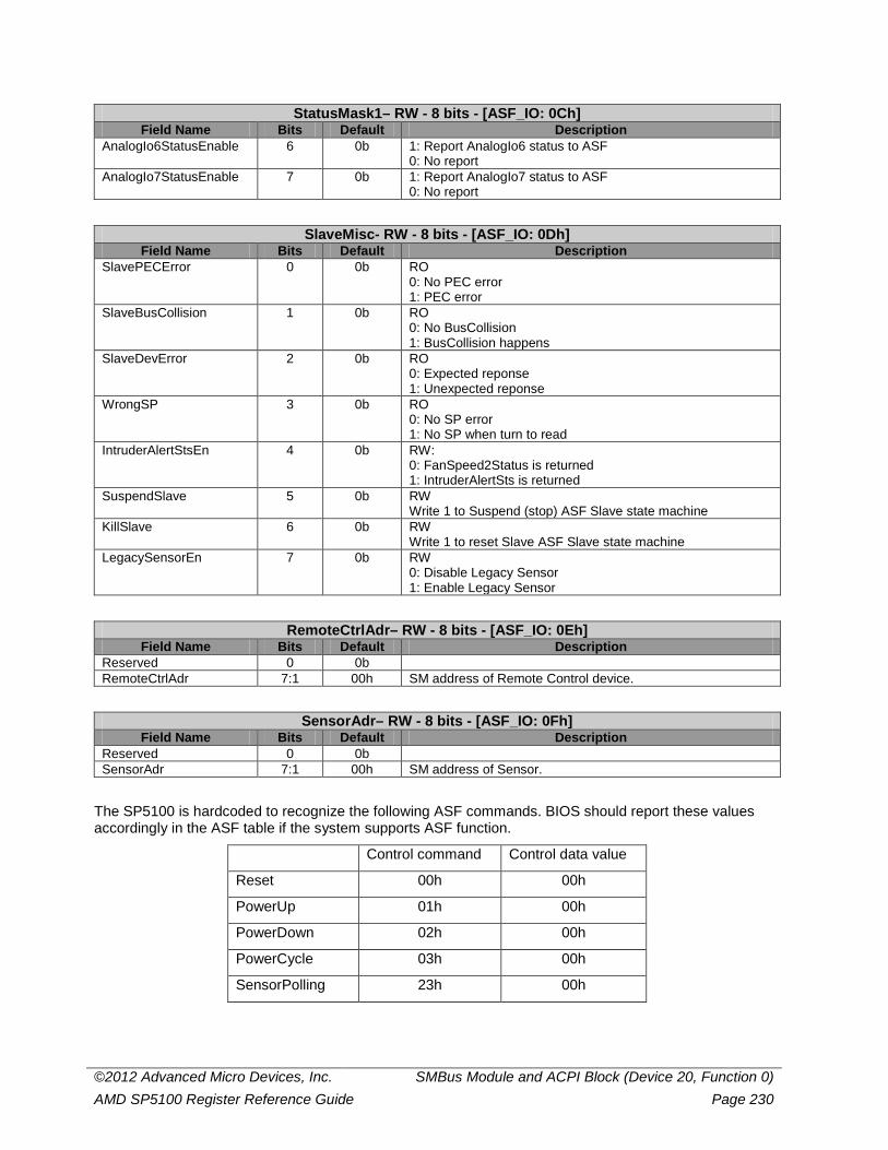
©2012 Advanced Micro Devices, Inc. SMBus Module and ACPI Block (Device 20, Function 0) AMD SP5100 Register Reference Guide Page 230
StatusMask1– RW - 8 bits - [ASF_IO: 0Ch] Field Name Bits Default Description
AnalogIo6StatusEnable 6 0b 1: Report AnalogIo6 status to ASF 0: No report
AnalogIo7StatusEnable 7 0b 1: Report AnalogIo7 status to ASF 0: No report
SlaveMisc- RW - 8 bits - [ASF_IO: 0Dh] Field Name Bits Default Description
SlavePECError 0 0b RO 0: No PEC error 1: PEC error
SlaveBusCollision 1 0b RO 0: No BusCollision 1: BusCollision happens
SlaveDevError 2 0b RO 0: Expected reponse 1: Unexpected reponse
WrongSP 3 0b RO 0: No SP error 1: No SP when turn to read
IntruderAlertStsEn 4 0b RW: 0: FanSpeed2Status is returned 1: IntruderAlertSts is returned
SuspendSlave 5 0b RW Write 1 to Suspend (stop) ASF Slave state machine
KillSlave 6 0b RW Write 1 to reset Slave ASF Slave state machine
LegacySensorEn 7 0b RW 0: Disable Legacy Sensor 1: Enable Legacy Sensor
RemoteCtrlAdr– RW - 8 bits - [ASF_IO: 0Eh] Field Name Bits Default Description
Reserved 0 0b RemoteCtrlAdr 7:1 00h SM address of Remote Control device.
SensorAdr– RW - 8 bits - [ASF_IO: 0Fh] Field Name Bits Default Description
Reserved 0 0b SensorAdr 7:1 00h SM address of Sensor.
The SP5100 is hardcoded to recognize the following ASF commands. BIOS should report these values accordingly in the ASF table if the system supports ASF function.
Control command Control data value
Reset 00h 00h
PowerUp 01h 00h
PowerDown 02h 00h
PowerCycle 03h 00h
SensorPolling 23h 00h
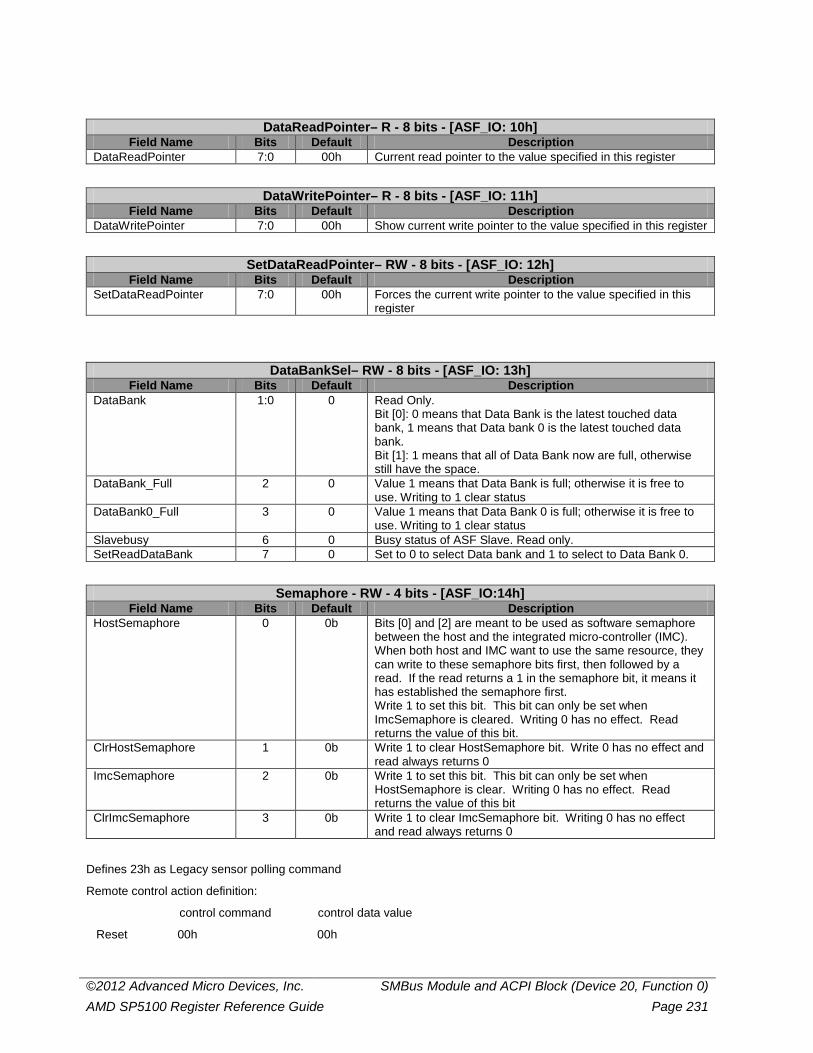
©2012 Advanced Micro Devices, Inc. SMBus Module and ACPI Block (Device 20, Function 0) AMD SP5100 Register Reference Guide Page 231
DataReadPointer– R - 8 bits - [ASF_IO: 10h] Field Name Bits Default Description
DataReadPointer 7:0 00h Current read pointer to the value specified in this register
DataWritePointer– R - 8 bits - [ASF_IO: 11h] Field Name Bits Default Description
DataWritePointer 7:0 00h Show current write pointer to the value specified in this register
SetDataReadPointer– RW - 8 bits - [ASF_IO: 12h] Field Name Bits Default Description
SetDataReadPointer 7:0 00h Forces the current write pointer to the value specified in this register
DataBankSel– RW - 8 bits - [ASF_IO: 13h] Field Name Bits Default Description
DataBank 1:0 0 Read Only. Bit [0]: 0 means that Data Bank is the latest touched data bank, 1 means that Data bank 0 is the latest touched data bank. Bit [1]: 1 means that all of Data Bank now are full, otherwise still have the space.
DataBank_Full 2 0 Value 1 means that Data Bank is full; otherwise it is free to use. Writing to 1 clear status
DataBank0_Full 3 0 Value 1 means that Data Bank 0 is full; otherwise it is free to use. Writing to 1 clear status
Slavebusy 6 0 Busy status of ASF Slave. Read only. SetReadDataBank 7 0 Set to 0 to select Data bank and 1 to select to Data Bank 0.
Semaphore - RW - 4 bits - [ASF_IO:14h] Field Name Bits Default Description
HostSemaphore 0 0b Bits [0] and [2] are meant to be used as software semaphore between the host and the integrated micro-controller (IMC). When both host and IMC want to use the same resource, they can write to these semaphore bits first, then followed by a read. If the read returns a 1 in the semaphore bit, it means it has established the semaphore first. Write 1 to set this bit. This bit can only be set when ImcSemaphore is cleared. Writing 0 has no effect. Read returns the value of this bit.
ClrHostSemaphore 1 0b Write 1 to clear HostSemaphore bit. Write 0 has no effect and read always returns 0
ImcSemaphore 2 0b Write 1 to set this bit. This bit can only be set when HostSemaphore is clear. Writing 0 has no effect. Read returns the value of this bit
ClrImcSemaphore 3 0b Write 1 to clear ImcSemaphore bit. Writing 0 has no effect and read always returns 0
Defines 23h as Legacy sensor polling command
Remote control action definition:
control command control data value
Reset 00h 00h
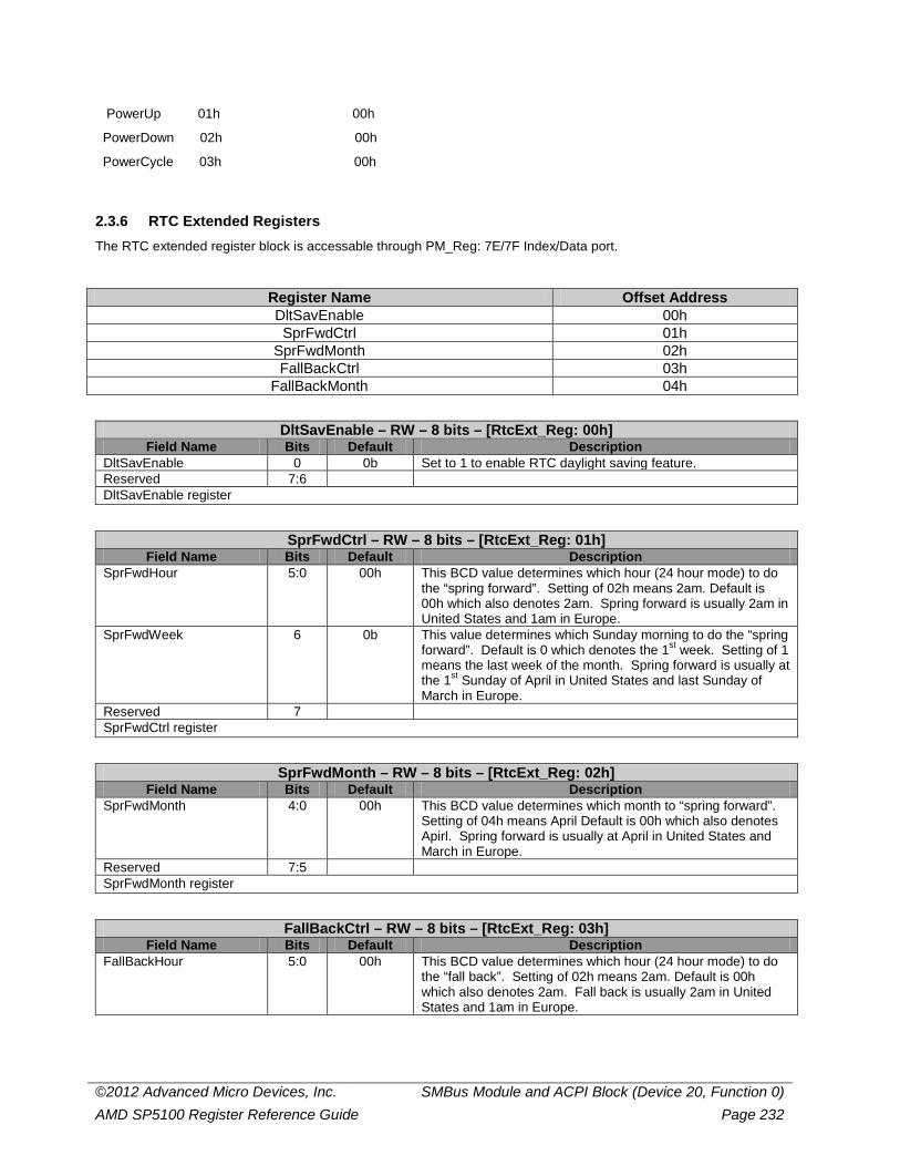
©2012 Advanced Micro Devices, Inc. SMBus Module and ACPI Block (Device 20, Function 0) AMD SP5100 Register Reference Guide Page 232
PowerUp 01h 00h
PowerDown 02h 00h
PowerCycle 03h 00h
2.3.6 RTC Extended Registers The RTC extended register block is accessable through PM_Reg: 7E/7F Index/Data port.
Register Name Offset Address DltSavEnable 00h SprFwdCtrl 01h
SprFwdMonth 02h FallBackCtrl 03h
FallBackMonth 04h
DltSavEnable – RW – 8 bits – [RtcExt_Reg: 00h] Field Name Bits Default Description
DltSavEnable 0 0b Set to 1 to enable RTC daylight saving feature. Reserved 7:6 DltSavEnable register
SprFwdCtrl – RW – 8 bits – [RtcExt_Reg: 01h] Field Name Bits Default Description
SprFwdHour 5:0 00h This BCD value determines which hour (24 hour mode) to do the “spring forward”. Setting of 02h means 2am. Default is 00h which also denotes 2am. Spring forward is usually 2am in United States and 1am in Europe.
SprFwdWeek 6 0b This value determines which Sunday morning to do the “spring forward”. Default is 0 which denotes the 1st week. Setting of 1 means the last week of the month. Spring forward is usually at the 1st Sunday of April in United States and last Sunday of March in Europe.
Reserved 7 SprFwdCtrl register
SprFwdMonth – RW – 8 bits – [RtcExt_Reg: 02h] Field Name Bits Default Description
SprFwdMonth 4:0 00h This BCD value determines which month to “spring forward”. Setting of 04h means April Default is 00h which also denotes Apirl. Spring forward is usually at April in United States and March in Europe.
Reserved 7:5 SprFwdMonth register
FallBackCtrl – RW – 8 bits – [RtcExt_Reg: 03h] Field Name Bits Default Description
FallBackHour 5:0 00h This BCD value determines which hour (24 hour mode) to do the “fall back”. Setting of 02h means 2am. Default is 00h which also denotes 2am. Fall back is usually 2am in United States and 1am in Europe.

©2012 Advanced Micro Devices, Inc. SMBus Module and ACPI Block (Device 20, Function 0) AMD SP5100 Register Reference Guide Page 233
FallBackCtrl – RW – 8 bits – [RtcExt_Reg: 03h] Field Name Bits Default Description
FallBackWeek 6 0b This value determines which Sunday morning to do the “fall back”. Default is 0 which denotes the last week. Setting of 1 means the first week of the month. Fall back is usually at the last Sunday of October in both United States and Europe.
Reserved 7 FallBackCtrl register
FallBackMonth – RW – 8 bits – [RtcExt_Reg: 04h]
Field Name Bits Default Description FallBackMonth 4:0 00h This BCD value determines which month to “fall back”. Setting
of 10h means October. Default is 00h which also denotes October. Fall back is usually at October in both United States and Europe.
Reserved 7:5 FallBackMonth register
Week Timer registers
The 16-bit Week Timer is a battery powered down counter timer that supports 1ms, 1 second and 1minute resolution and auto reloads when the timer reaches 0. The WEEK_ALRM interrupt is asserted when the timer reaches 0 and stays asserted until the timer is disabled. The Week Timer registers are located in RTC extended register block index 10h through 14h.
WeekTimerControl – RW – 8 bits – [RtcExt_Reg: 10h] Field Name Bits Default Description
Enable 0 0b This bit is used to start and stop the Week Timer. 0: Disable 1: Enable
Resolution 2:1 00b These bits are used to control the resolution of the Week Timer counter. 00: 1 minute 01: 1 second 10: 1ms 11: Reserved
Reserved 7:3 WeekTimerControl register Note: The Enable should be cleared when changing the Resolution setting.
WeekTimerReloadLow – RW – 8 bits – [RtcExt_Reg: 11h]
Field Name Bits Default Description WeekTimerReloadLow 7:0 This register is used to program the lower 8 bits of the 16-bit
WeekTimerReload register. Writing the WeekTimerReloadLow register causes the 16-bit WeekTimerReload to be written into the Week Timer.
WeekTimerReloadLow register Note: The Enable in the WeekTimerControl register should be cleared before performing a write access to the WeekTimerReloadLow or WeekTimerReload High register.
WeekTimerReloadHigh – RW – 8 bits – [RtcExt_Reg: 12h]
Field Name Bits Default Description WeekTimerReloadHigh 7:0 This register is used to program the upper 8 bits of the 16-bit
WeekTimerReload register. This register should be programmed before writing the WeekTimerReloadLow register.
WeekTimerReloadHigh register Note: The Enable in the WeekTimerControl register should be cleared before performing a write access to the WeekTimerReloadLow or WeekTimerReload High register.

©2012 Advanced Micro Devices, Inc. SMBus Module and ACPI Block (Device 20, Function 0) AMD SP5100 Register Reference Guide Page 234
WeekTimerDataLow – R – 8 bits – [RtcExt_Reg: 13h] Field Name Bits Default Description
WeekTimerDataLow 7:0 This register is used to read the current state of the 16-bit Week Timer. Reading from the WeekTimerDataLow register returns the lower 8 bits of the 16-bit Week Timer and cause the upper 8 bits to be latched into the WeekTimerDataHigh register.
WeekTimerDataLow register Note: Two reads are required to read the current state of the 16-bit Week Timer: the first read from the WeekTimerDataLow register returns the lower 8 bits of the 16-bit Week Timer and the second read from the WeekTimerDataHigh register return the upper 8 bits of the 16-bit Week Timer.
WeekTimerDataHigh – R – 8 bits – [RtcExt_Reg: 14h]
Field Name Bits Default Description WeekTimerDataHigh 7:0 This register is used to read the current state of the 16-bit
Week Timer. Reading from the WeekTimerDataHigh register returns the upper 8 bits of the 16-bit Week Timer latched by a previous read from the WeekTimerDataLow register.
WeekTimerDataLow register Note: Two reads are required to read the current state of the 16-bit Week Timer: the first read from the WeekTimerDataLow register returns the lower 8 bits of the 16-bit Week Timer and the second read from the WeekTimerDataHigh register return the upper 8 bits of the 16-bit Week Timer.
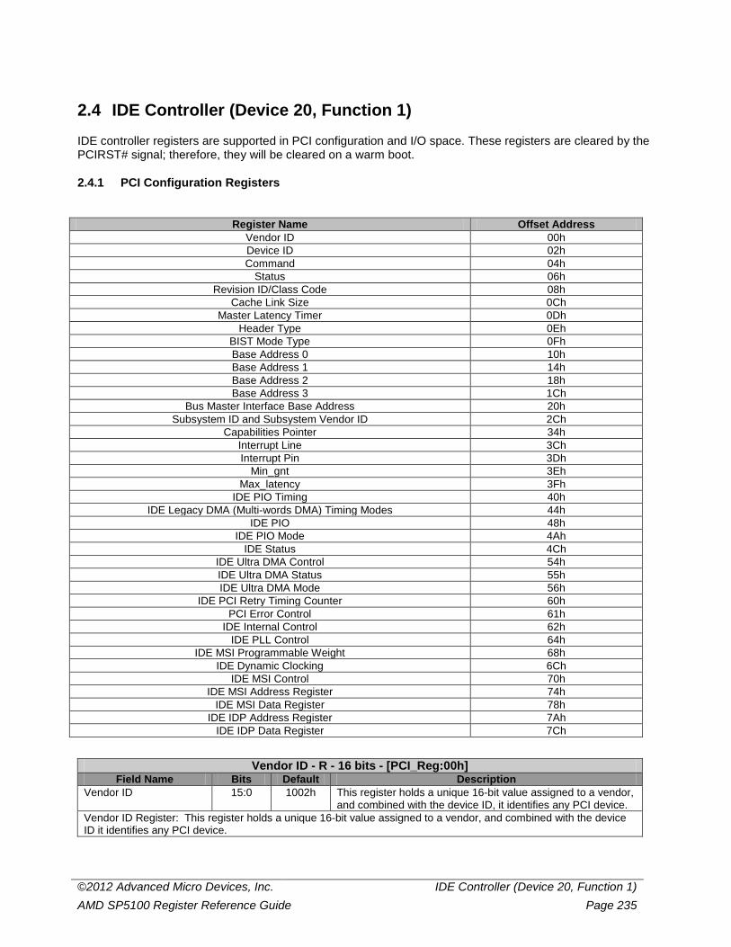
©2012 Advanced Micro Devices, Inc. IDE Controller (Device 20, Function 1) AMD SP5100 Register Reference Guide Page 235
2.4 IDE Controller (Device 20, Function 1)
IDE controller registers are supported in PCI configuration and I/O space. These registers are cleared by the PCIRST# signal; therefore, they will be cleared on a warm boot.
2.4.1 PCI Configuration Registers
Register Name Offset Address Vendor ID 00h Device ID 02h Command 04h
Status 06h Revision ID/Class Code 08h
Cache Link Size 0Ch Master Latency Timer 0Dh
Header Type 0Eh BIST Mode Type 0Fh Base Address 0 10h Base Address 1 14h Base Address 2 18h Base Address 3 1Ch
Bus Master Interface Base Address 20h Subsystem ID and Subsystem Vendor ID 2Ch
Capabilities Pointer 34h Interrupt Line 3Ch Interrupt Pin 3Dh
Min_gnt 3Eh Max_latency 3Fh
IDE PIO Timing 40h IDE Legacy DMA (Multi-words DMA) Timing Modes 44h
IDE PIO 48h IDE PIO Mode 4Ah
IDE Status 4Ch IDE Ultra DMA Control 54h IDE Ultra DMA Status 55h IDE Ultra DMA Mode 56h
IDE PCI Retry Timing Counter 60h PCI Error Control 61h
IDE Internal Control 62h IDE PLL Control 64h
IDE MSI Programmable Weight 68h IDE Dynamic Clocking 6Ch
IDE MSI Control 70h IDE MSI Address Register 74h
IDE MSI Data Register 78h IDE IDP Address Register 7Ah
IDE IDP Data Register 7Ch
Vendor ID - R - 16 bits - [PCI_Reg:00h] Field Name Bits Default Description
Vendor ID 15:0 1002h This register holds a unique 16-bit value assigned to a vendor, and combined with the device ID, it identifies any PCI device.
Vendor ID Register: This register holds a unique 16-bit value assigned to a vendor, and combined with the device ID it identifies any PCI device.
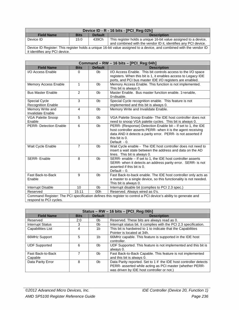
©2012 Advanced Micro Devices, Inc. IDE Controller (Device 20, Function 1) AMD SP5100 Register Reference Guide Page 236
Device ID - R - 16 bits - [PCI_Reg:02h] Field Name Bits Default Description
Device ID 15:0 439Ch This register holds a unique 16-bit value assigned to a device, and combined with the vendor ID it, identifies any PCI device.
Device ID Register: This register holds a unique 16-bit value assigned to a device, and combined with the vendor ID it identifies any PCI device.
Command – RW – 16 bits – [PCI_Reg:04h] Field Name Bits Default Description
I/O Access Enable 0 0b I/O Access Enable. This bit controls access to the I/O space registers. When this bit is 1, it enables access to Legacy IDE ports, and PCI bus master IDE I/O registers are enabled.
Memory Access Enable 1 0b Memory Access Enable. This function is not implemented. This bit is always 0.
Bus Master Enable 2 0b Master Enable. Bus master function enable. 1=enable, 0=disable.
Special Cycle Recognition Enable
3 0b Special Cycle recognition enable. This feature is not implemented and this bit is always 0.
Memory Write and Invalidate Enable
4 0b Memory Write and Invalidate Enable.
VGA Palette Snoop Enable
5 0b VGA Palette Snoop Enable- The IDE host controller does not need to snoop VGA palette cycles. This bit is always 0.
PERR- Detection Enable 6 0b PERR- (Response) Detection Enable bit – If set to 1, the IDE host controller asserts PERR- when it is the agent receiving data AND it detects a parity error. PERR- is not asserted if this bit is 0. Default - 0.
Wait Cycle Enable 7 0b Wait Cycle enable - The IDE host controller does not need to insert a wait state between the address and data on the AD lines. This bit is always 0.
SERR- Enable 8 0b SERR- enable – If set to 1, the IDE host controller asserts SERR- when it detects an address parity error. SERR- is not asserted if this bit is 0. Default – 0.
Fast Back-to-Back Enable
9 0b Fast Back-to-back enable. The IDE host controller only acts as a master to a single device, so this functionality is not needed. This bit is always 0.
Interrupt Disable 10 0b Interrupt disable bit (complies to PCI 2.3 spec.) Reserved 15:11 00h Reserved. Always wired as 0’s. Command Register: The PCI specification defines this register to control a PCI device’s ability to generate and respond to PCI cycles.
Status – RW – 16 bits – [PCI_Reg:06h] Field Name Bits Default Description
Reserved 2:0 0b Reserved. These bits are always read as 0. Interrupt Status 3 0b Interrupt status bit. It complies with the PCI 2.3 specification. Capabilities List 4 1b This bit is hardwired to 1 to indicate that the Capabilities
Pointer is located at 34h. 66MHz Support 5 1b 66MHz capable. This feature is supported in the IDE host
controller. UDF Supported 6 0b UDF Supported. This feature is not implemented and this bit is
always 0. Fast Back-to-Back Capable
7 0b Fast Back-to-Back Capable. This feature is not implemented and this bit is always 0.
Data Parity Error 8 0b Data Parity reported. Set to 1 if the IDE host controller detects PERR- asserted while acting as PCI master (whether PERR- was driven by IDE host controller or not.)
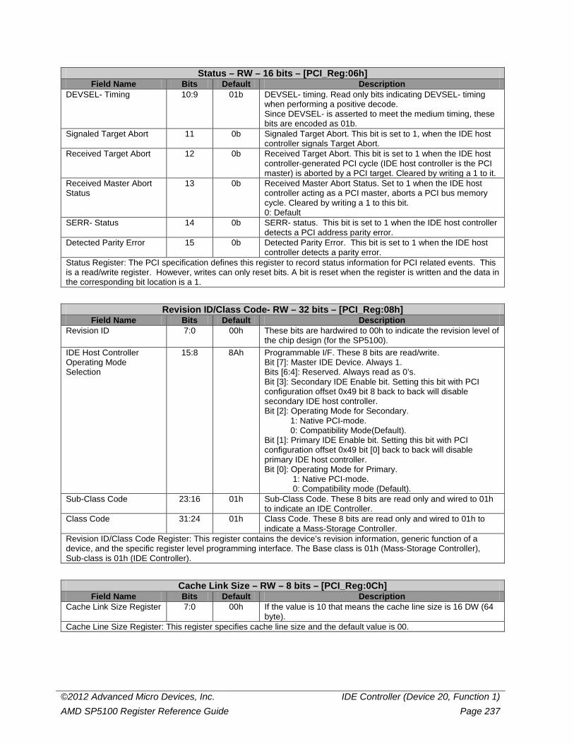
©2012 Advanced Micro Devices, Inc. IDE Controller (Device 20, Function 1) AMD SP5100 Register Reference Guide Page 237
Status – RW – 16 bits – [PCI_Reg:06h] Field Name Bits Default Description
DEVSEL- Timing 10:9 01b DEVSEL- timing. Read only bits indicating DEVSEL- timing when performing a positive decode. Since DEVSEL- is asserted to meet the medium timing, these bits are encoded as 01b.
Signaled Target Abort 11 0b Signaled Target Abort. This bit is set to 1, when the IDE host controller signals Target Abort.
Received Target Abort 12 0b Received Target Abort. This bit is set to 1 when the IDE host controller-generated PCI cycle (IDE host controller is the PCI master) is aborted by a PCI target. Cleared by writing a 1 to it.
Received Master Abort Status
13 0b Received Master Abort Status. Set to 1 when the IDE host controller acting as a PCI master, aborts a PCI bus memory cycle. Cleared by writing a 1 to this bit. 0: Default
SERR- Status 14 0b SERR- status. This bit is set to 1 when the IDE host controller detects a PCI address parity error.
Detected Parity Error 15 0b Detected Parity Error. This bit is set to 1 when the IDE host controller detects a parity error.
Status Register: The PCI specification defines this register to record status information for PCI related events. This is a read/write register. However, writes can only reset bits. A bit is reset when the register is written and the data in the corresponding bit location is a 1.
Revision ID/Class Code- RW – 32 bits – [PCI_Reg:08h] Field Name Bits Default Description
Revision ID 7:0 00h These bits are hardwired to 00h to indicate the revision level of the chip design (for the SP5100).
IDE Host Controller Operating Mode Selection
15:8 8Ah Programmable I/F. These 8 bits are read/write. Bit [7]: Master IDE Device. Always 1. Bits [6:4]: Reserved. Always read as 0’s. Bit [3]: Secondary IDE Enable bit. Setting this bit with PCI configuration offset 0x49 bit 8 back to back will disable secondary IDE host controller. Bit [2]: Operating Mode for Secondary. 1: Native PCI-mode. 0: Compatibility Mode(Default). Bit [1]: Primary IDE Enable bit. Setting this bit with PCI configuration offset 0x49 bit [0] back to back will disable primary IDE host controller. Bit [0]: Operating Mode for Primary. 1: Native PCI-mode. 0: Compatibility mode (Default).
Sub-Class Code 23:16 01h Sub-Class Code. These 8 bits are read only and wired to 01h to indicate an IDE Controller.
Class Code 31:24 01h Class Code. These 8 bits are read only and wired to 01h to indicate a Mass-Storage Controller.
Revision ID/Class Code Register: This register contains the device’s revision information, generic function of a device, and the specific register level programming interface. The Base class is 01h (Mass-Storage Controller), Sub-class is 01h (IDE Controller).
Cache Link Size – RW – 8 bits – [PCI_Reg:0Ch] Field Name Bits Default Description
Cache Link Size Register 7:0 00h If the value is 10 that means the cache line size is 16 DW (64 byte).
Cache Line Size Register: This register specifies cache line size and the default value is 00.
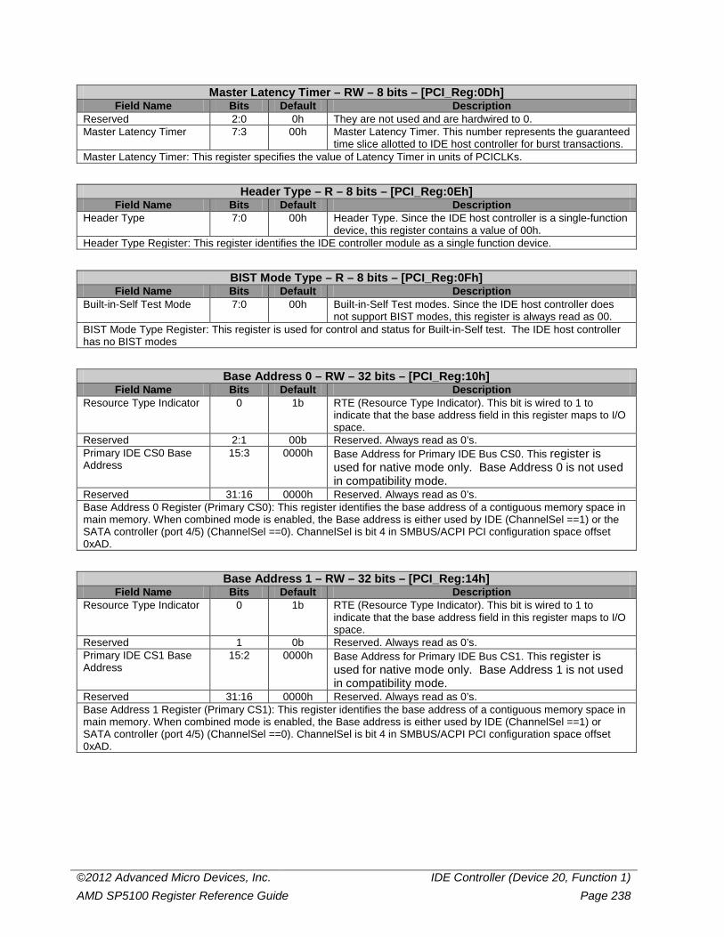
©2012 Advanced Micro Devices, Inc. IDE Controller (Device 20, Function 1) AMD SP5100 Register Reference Guide Page 238
Master Latency Timer – RW – 8 bits – [PCI_Reg:0Dh] Field Name Bits Default Description
Reserved 2:0 0h They are not used and are hardwired to 0. Master Latency Timer 7:3 00h Master Latency Timer. This number represents the guaranteed
time slice allotted to IDE host controller for burst transactions. Master Latency Timer: This register specifies the value of Latency Timer in units of PCICLKs.
Header Type – R – 8 bits – [PCI_Reg:0Eh] Field Name Bits Default Description
Header Type 7:0 00h Header Type. Since the IDE host controller is a single-function device, this register contains a value of 00h.
Header Type Register: This register identifies the IDE controller module as a single function device.
BIST Mode Type – R – 8 bits – [PCI_Reg:0Fh] Field Name Bits Default Description
Built-in-Self Test Mode 7:0 00h Built-in-Self Test modes. Since the IDE host controller does not support BIST modes, this register is always read as 00.
BIST Mode Type Register: This register is used for control and status for Built-in-Self test. The IDE host controller has no BIST modes
Base Address 0 – RW – 32 bits – [PCI_Reg:10h] Field Name Bits Default Description
Resource Type Indicator 0 1b RTE (Resource Type Indicator). This bit is wired to 1 to indicate that the base address field in this register maps to I/O space.
Reserved 2:1 00b Reserved. Always read as 0’s. Primary IDE CS0 Base Address
15:3 0000h Base Address for Primary IDE Bus CS0. This register is used for native mode only. Base Address 0 is not used in compatibility mode.
Reserved 31:16 0000h Reserved. Always read as 0’s. Base Address 0 Register (Primary CS0): This register identifies the base address of a contiguous memory space in main memory. When combined mode is enabled, the Base address is either used by IDE (ChannelSel ==1) or the SATA controller (port 4/5) (ChannelSel ==0). ChannelSel is bit 4 in SMBUS/ACPI PCI configuration space offset 0xAD.
Base Address 1 – RW – 32 bits – [PCI_Reg:14h] Field Name Bits Default Description
Resource Type Indicator 0 1b RTE (Resource Type Indicator). This bit is wired to 1 to indicate that the base address field in this register maps to I/O space.
Reserved 1 0b Reserved. Always read as 0’s. Primary IDE CS1 Base Address
15:2 0000h Base Address for Primary IDE Bus CS1. This register is used for native mode only. Base Address 1 is not used in compatibility mode.
Reserved 31:16 0000h Reserved. Always read as 0’s. Base Address 1 Register (Primary CS1): This register identifies the base address of a contiguous memory space in main memory. When combined mode is enabled, the Base address is either used by IDE (ChannelSel ==1) or SATA controller (port 4/5) (ChannelSel ==0). ChannelSel is bit 4 in SMBUS/ACPI PCI configuration space offset 0xAD.
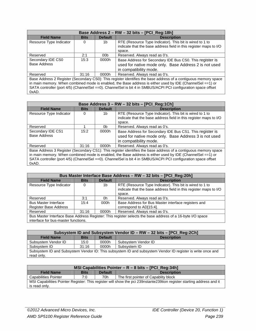
©2012 Advanced Micro Devices, Inc. IDE Controller (Device 20, Function 1) AMD SP5100 Register Reference Guide Page 239
Base Address 2 – RW – 32 bits – [PCI_Reg:18h] Field Name Bits Default Description
Resource Type Indicator 0 1b RTE (Resource Type Indicator). This bit is wired to 1 to indicate that the base address field in this register maps to I/O space.
Reserved 2:1 00b Reserved. Always read as 0’s. Secondary IDE CS0 Base Address
15:3 0000h Base Address for Secondary IDE Bus CS0. This register is used for native mode only. Base Address 2 is not used in compatibility mode.
Reserved 31:16 0000h Reserved. Always read as 0’s. Base Address 2 Register (Secondary CS0): This register identifies the base address of a contiguous memory space in main memory. When combined mode is enabled, the Base address is either used by IDE (ChannelSel ==1) or SATA controller (port 4/5) (ChannelSel ==0). ChannelSel is bit 4 in SMBUS/ACPI PCI configuration space offset 0xAD.
Base Address 3 – RW – 32 bits – [PCI_Reg:1Ch] Field Name Bits Default Description
Resource Type Indicator 0 1b RTE (Resource Type Indicator). This bit is wired to 1 to indicate that the base address field in this register maps to I/O space.
Reserved 1 0b Reserved. Always read as 0’s. Secondary IDE CS1 Base Address
15:2 0000h Base Address for Secondary IDE Bus CS1. This register is used for native mode only. Base Address 3 is not used in compatibility mode.
Reserved 31:16 0000h Reserved. Always read as 0’s. Base Address 3 Register (Secondary CS1): This register identifies the base address of a contiguous memory space in main memory. When combined mode is enabled, the Base address is either used by IDE (ChannelSel ==1) or SATA controller (port 4/5) (ChannelSel ==0). ChannelSel is bit 4 in SMBUS/ACPI PCI configuration space offset 0xAD.
Bus Master Interface Base Address – RW – 32 bits – [PCI_Reg:20h] Field Name Bits Default Description
Resource Type Indicator 0 1b RTE (Resource Type Indicator). This bit is wired to 1 to indicate that the base address field in this register maps to I/O space.
Reserved 3:1 0h Reserved. Always read as 0’s. Bus Master Interface Register Base Address
15:4 000h Base Address for Bus Master interface registers and correspond to AD[15:4].
Reserved 31:16 0000h Reserved. Always read as 0’s. Bus Master Interface Base Address Register: This register selects the base address of a 16-byte I/O space interface for bus-master functions.
Subsystem ID and Subsystem Vendor ID – RW – 32 bits – [PCI_Reg:2Ch] Field Name Bits Default Description
Subsystem Vendor ID 15:0 0000h Subsystem Vendor ID Subsystem ID 31:16 0000h Subsystem ID Subsystem ID and Subsystem Vendor ID: This subsystem ID and subsystem Vendor ID register is write once and read only.
MSI Capabilities Pointer – R – 8 bits – [PCI_Reg:34h] Field Name Bits Default Description
Capabilities Pointer 7:0 70h The first pointer of Capablity block MSI Capabilities Pointer Register: This register will show the pci 239nstante239tion register starting address and it is read only.
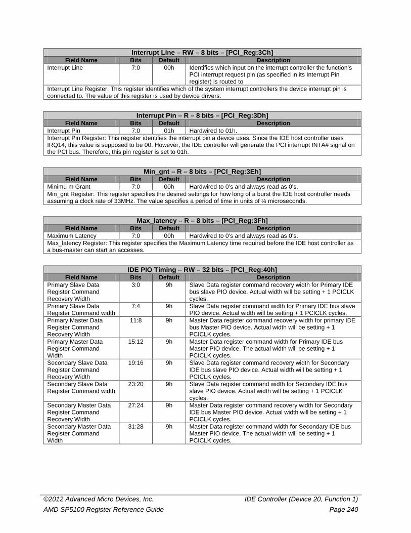
©2012 Advanced Micro Devices, Inc. IDE Controller (Device 20, Function 1) AMD SP5100 Register Reference Guide Page 240
Interrupt Line – RW – 8 bits – [PCI_Reg:3Ch] Field Name Bits Default Description
Interrupt Line 7:0 00h Identifies which input on the interrupt controller the function’s PCI interrupt request pin (as specified in its Interrupt Pin register) is routed to
Interrupt Line Register: This register identifies which of the system interrupt controllers the device interrupt pin is connected to. The value of this register is used by device drivers.
Interrupt Pin – R – 8 bits – [PCI_Reg:3Dh] Field Name Bits Default Description
Interrupt Pin 7:0 01h Hardwired to 01h. Interrupt Pin Register: This register identifies the interrupt pin a device uses. Since the IDE host controller uses IRQ14, this value is supposed to be 00. However, the IDE controller will generate the PCI interrupt INTA# signal on the PCI bus. Therefore, this pin register is set to 01h.
Min_gnt – R – 8 bits – [PCI_Reg:3Eh] Field Name Bits Default Description
Minimu m Grant 7:0 00h Hardwired to 0’s and always read as 0’s. Min_gnt Register: This register specifies the desired settings for how long of a burst the IDE host controller needs assuming a clock rate of 33MHz. The value specifies a period of time in units of ¼ microseconds.
Max_latency – R – 8 bits – [PCI_Reg:3Fh] Field Name Bits Default Description
Maximum Latency 7:0 00h Hardwired to 0’s and always read as 0’s. Max_latency Register: This register specifies the Maximum Latency time required before the IDE host controller as a bus-master can start an accesses.
IDE PIO Timing – RW – 32 bits – [PCI_Reg:40h] Field Name Bits Default Description
Primary Slave Data Register Command Recovery Width
3:0 9h Slave Data register command recovery width for Primary IDE bus slave PIO device. Actual width will be setting + 1 PCICLK cycles.
Primary Slave Data Register Command width
7:4 9h Slave Data register command width for Primary IDE bus slave PIO device. Actual width will be setting + 1 PCICLK cycles.
Primary Master Data Register Command Recovery Width
11:8 9h Master Data register command recovery width for primary IDE bus Master PIO device. Actual width will be setting + 1 PCICLK cycles.
Primary Master Data Register Command Width
15:12 9h Master Data register command width for Primary IDE bus Master PIO device. The actual width will be setting + 1 PCICLK cycles.
Secondary Slave Data Register Command Recovery Width
19:16 9h Slave Data register command recovery width for Secondary IDE bus slave PIO device. Actual width will be setting + 1 PCICLK cycles.
Secondary Slave Data Register Command width
23:20 9h Slave Data register command width for Secondary IDE bus slave PIO device. Actual width will be setting + 1 PCICLK cycles.
Secondary Master Data Register Command Recovery Width
27:24 9h Master Data register command recovery width for Secondary IDE bus Master PIO device. Actual width will be setting + 1 PCICLK cycles.
Secondary Master Data Register Command Width
31:28 9h Master Data register command width for Secondary IDE bus Master PIO device. The actual width will be setting + 1 PCICLK cycles.
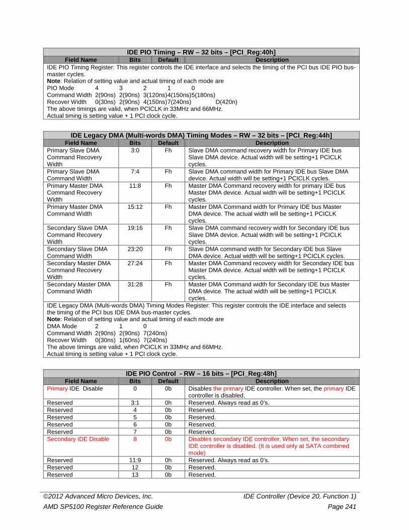
©2012 Advanced Micro Devices, Inc. IDE Controller (Device 20, Function 1) AMD SP5100 Register Reference Guide Page 241
IDE PIO Timing – RW – 32 bits – [PCI_Reg:40h] Field Name Bits Default Description
IDE PIO Timing Register: This register controls the IDE interface and selects the timing of the PCI bus IDE PIO bus-master cycles. Note: Relation of setting value and actual timing of each mode are PIO Mode 4 3 2 1 0 Command Width 2(90ns) 2(90ns) 3(120ns) 4(150ns) 5(180ns) Recover Width 0(30ns) 2(90ns) 4(150ns) 7(240ns) D(420n) The above timings are valid, when PCICLK in 33MHz and 66MHz. Actual timing is setting value + 1 PCI clock cycle.
IDE Legacy DMA (Multi-words DMA) Timing Modes – RW – 32 bits – [PCI_Reg:44h] Field Name Bits Default Description
Primary Slave DMA Command Recovery Width
3:0 Fh Slave DMA command recovery width for Primary IDE bus Slave DMA device. Actual width will be setting+1 PCICLK cycles.
Primary Slave DMA Command Width
7:4 Fh Slave DMA command width for Primary IDE bus Slave DMA device. Actual width will be setting+1 PCICLK cycles.
Primary Master DMA Command Recovery Width
11:8 Fh Master DMA Command recovery width for primary IDE bus Master DMA device. Actual width will be setting+1 PCICLK cycles.
Primary Master DMA Command Width
15:12 Fh Master DMA Command width for Primary IDE bus Master DMA device. The actual width will be setting+1 PCICLK cycles.
Secondary Slave DMA Command Recovery Width
19:16 Fh Slave DMA command recovery width for Secondary IDE bus Slave DMA device. Actual width will be setting+1 PCICLK cycles.
Secondary Slave DMA Command Width
23:20 Fh Slave DMA command width for Secondary IDE bus Slave DMA device. Actual width will be setting+1 PCICLK cycles.
Secondary Master DMA Command Recovery Width
27:24 Fh Master DMA Command recovery width for Secondary IDE bus Master DMA device. Actual width will be setting+1 PCICLK cycles.
Secondary Master DMA Command Width
31:28 Fh Master DMA Command width for Secondary IDE bus Master DMA device. The actual width will be setting+1 PCICLK cycles.
IDE Legacy DMA (Multi-words DMA) Timing Modes Register: This register controls the IDE interface and selects the timing of the PCI bus IDE DMA bus-master cycles. Note: Relation of setting value and actual timing of each mode are DMA Mode 2 1 0 Command Width 2(90ns) 2(90ns) 7(240ns) Recover Width 0(30ns) 1(60ns) 7(240ns) The above timings are valid, when PCICLK in 33MHz and 66MHz. Actual timing is setting value + 1 PCI clock cycle.
IDE PIO Control - RW – 16 bits – [PCI_Reg:48h] Field Name Bits Default Description
Primary IDE Disable 0 0b Disables the primary IDE controller. When set, the primary IDE controller is disabled.
Reserved 3:1 0h Reserved. Always read as 0’s. Reserved 4 0b Reserved. Reserved 5 0b Reserved. Reserved 6 0b Reserved. Reserved 7 0b Reserved. Secondary IDE Disable 8 0b Disables secondary IDE controller. When set, the secondary
IDE controller is disabled. (It is used only at SATA combined mode)
Reserved 11:9 0h Reserved. Always read as 0’s. Reserved 12 0b Reserved. Reserved 13 0b Reserved.
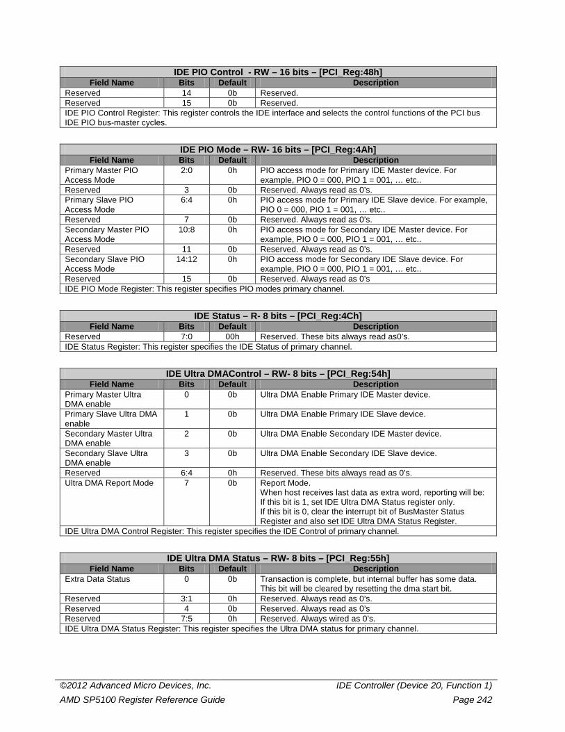
©2012 Advanced Micro Devices, Inc. IDE Controller (Device 20, Function 1) AMD SP5100 Register Reference Guide Page 242
IDE PIO Control - RW – 16 bits – [PCI_Reg:48h] Field Name Bits Default Description
Reserved 14 0b Reserved. Reserved 15 0b Reserved. IDE PIO Control Register: This register controls the IDE interface and selects the control functions of the PCI bus IDE PIO bus-master cycles.
IDE PIO Mode – RW- 16 bits – [PCI_Reg:4Ah] Field Name Bits Default Description
Primary Master PIO Access Mode
2:0 0h PIO access mode for Primary IDE Master device. For example, PIO 0 = 000, PIO 1 = 001, … etc..
Reserved 3 0b Reserved. Always read as 0’s. Primary Slave PIO Access Mode
6:4 0h PIO access mode for Primary IDE Slave device. For example, PIO 0 = 000, PIO 1 = 001, … etc..
Reserved 7 0b Reserved. Always read as 0’s. Secondary Master PIO Access Mode
10:8 0h PIO access mode for Secondary IDE Master device. For example, PIO 0 = 000, PIO 1 = 001, … etc..
Reserved 11 0b Reserved. Always read as 0’s. Secondary Slave PIO Access Mode
14:12 0h PIO access mode for Secondary IDE Slave device. For example, PIO 0 = 000, PIO 1 = 001, … etc..
Reserved 15 0b Reserved. Always read as 0’s IDE PIO Mode Register: This register specifies PIO modes primary channel.
IDE Status – R- 8 bits – [PCI_Reg:4Ch] Field Name Bits Default Description
Reserved 7:0 00h Reserved. These bits always read as0’s. IDE Status Register: This register specifies the IDE Status of primary channel.
IDE Ultra DMAControl – RW- 8 bits – [PCI_Reg:54h] Field Name Bits Default Description
Primary Master Ultra DMA enable
0 0b Ultra DMA Enable Primary IDE Master device.
Primary Slave Ultra DMA enable
1 0b Ultra DMA Enable Primary IDE Slave device.
Secondary Master Ultra DMA enable
2 0b Ultra DMA Enable Secondary IDE Master device.
Secondary Slave Ultra DMA enable
3 0b Ultra DMA Enable Secondary IDE Slave device.
Reserved 6:4 0h Reserved. These bits always read as 0’s. Ultra DMA Report Mode 7 0b Report Mode.
When host receives last data as extra word, reporting will be: If this bit is 1, set IDE Ultra DMA Status register only. If this bit is 0, clear the interrupt bit of BusMaster Status Register and also set IDE Ultra DMA Status Register.
IDE Ultra DMA Control Register: This register specifies the IDE Control of primary channel.
IDE Ultra DMA Status – RW- 8 bits – [PCI_Reg:55h] Field Name Bits Default Description
Extra Data Status 0 0b Transaction is complete, but internal buffer has some data. This bit will be cleared by resetting the dma start bit.
Reserved 3:1 0h Reserved. Always read as 0’s. Reserved 4 0b Reserved. Always read as 0’s Reserved 7:5 0h Reserved. Always wired as 0’s. IDE Ultra DMA Status Register: This register specifies the Ultra DMA status for primary channel.
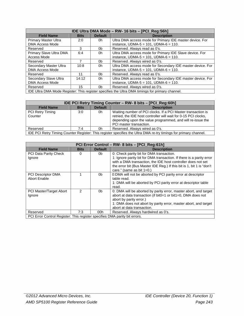
©2012 Advanced Micro Devices, Inc. IDE Controller (Device 20, Function 1) AMD SP5100 Register Reference Guide Page 243
IDE Ultra DMA Mode – RW- 16 bits – [PCI_Reg:56h] Field Name Bits Default Description
Primary Master Ultra DMA Access Mode
2:0 0h Ultra DMA access mode for Primary IDE master device. For instance, UDMA-5 = 101, UDMA-6 = 110.
Reserved 3 0b Reserved. Always read as 0’s. Primary Slave Ultra DMA Access Mode
6:4 0h Ultra DMA access mode for Primary IDE Slave device. For instance, UDMA-5 = 101, UDMA-6 = 110.
Reserved 7 0b Reserved. Always wired as 0’s. Secondary Master Ultra DMA Access Mode
10:8 0h Ultra DMA access mode for Secondary IDE master device. For instance, UDMA-5 = 101, UDMA-6 = 110.
Reserved 11 0b Reserved. Always read as 0’s. Secondary Slave Ultra DMA Access Mode
14:12 0h Ultra DMA access mode for Secondary IDE master device. For instance, UDMA-5 = 101, UDMA-6 = 110.
Reserved 15 0b Reserved. Always wired as 0’s. IDE Ultra DMA Mode Register: This register specifies the Ultra DMA timings for primary channel.
IDE PCI Retry Timing Counter – RW- 8 bits – [PCI_Reg:60h] Field Name Bits Default Description
PCI Retry Timing Counter
3:0 0h Waiting number of PCI clocks. If a PCI Master transaction is retried, the IDE host controller will wait for 0-15 PCI clocks, depending upon the value programmed, and will re-issue the PCI master transaction.
Reserved 7:4 0h Reserved. Always wired as 0’s. IDE PCI Retry Timing Counter Register: This register specifies the Ultra DMA re-try timings for primary channel.
PCI Error Control – RW- 8 bits – [PCI_Reg:61h] Field Name Bits Default Description
PCI Data Parity Check Ignore
0 0b 0: Check parity bit for DMA transaction. 1: Ignore parity bit for DMA transaction. If there is a parity error with a DMA transaction, the IDE host controller does not set the error bit (Bus Master IDE Reg.) If this bit is 1, bit 1 is “don’t care.” (same as bit 1=0.)
PCI Descriptor DMA Abort Enable
1 0b 0:DMA will not be aborted by PCI parity error at descriptor table read. 1: DMA will be aborted by PCI parity error at descriptor table read.
PCI Master/Target Abort Ignore
2 0b 0: DMA will be aborted by parity error, master abort, and target abort at data transaction (if bit0=1 or bit1=0, DMA does not abort by parity error.) 1: DMA does not abort by parity error, master abort, and target abort at data transaction.
Reserved 7:3 00h Reserved. Always hardwired as 0’s. PCI Error Control Register: This register specifies DMA parity bit errors.
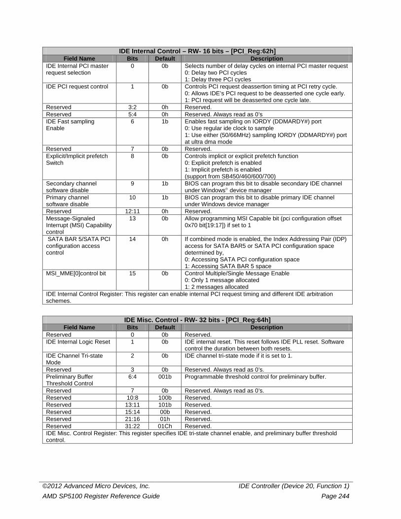
©2012 Advanced Micro Devices, Inc. IDE Controller (Device 20, Function 1) AMD SP5100 Register Reference Guide Page 244
IDE Internal Control – RW- 16 bits – [PCI_Reg:62h] Field Name Bits Default Description
IDE Internal PCI master request selection
0 0b Selects number of delay cycles on internal PCI master request 0: Delay two PCI cycles 1: Delay three PCI cycles
IDE PCI request control 1 0b Controls PCI request deassertion timing at PCI retry cycle. 0: Allows IDE’s PCI request to be deasserted one cycle early. 1: PCI request will be deasserted one cycle late.
Reserved 3:2 0h Reserved. Reserved 5:4 0h Reserved. Always read as 0’s IDE Fast sampling Enable
6 1b Enables fast sampling on IORDY (DDMARDY#) port 0: Use regular ide clock to sample 1: Use either (50/66MHz) sampling IORDY (DDMARDY#) port at ultra dma mode
Reserved 7 0b Reserved. Explicit/Implicit prefetch Switch
8 0b Controls implicit or explicit prefetch function 0: Explicit prefetch is enabled 1: Implicit prefetch is enabled (support from SB450/460/600/700)
Secondary channel software disable
9 1b BIOS can program this bit to disable secondary IDE channel under Windows device manager
Primary channel software disable
10 1b BIOS can program this bit to disable primary IDE channel under Windows device manager
Reserved 12:11 0h Reserved. Message-Signaled Interrupt (MSI) Capability control
13 0b Allow programming MSI Capable bit (pci configuration offset 0x70 bit[19:17]) if set to 1
SATA BAR 5/SATA PCI configuration access control
14 0h If combined mode is enabled, the Index Addressing Pair (IDP) access for SATA BAR5 or SATA PCI configuration space determined by, 0: Accessing SATA PCI configuration space 1: Accessing SATA BAR 5 space
MSI_MME[0]control bit 15 0b Control Multiple/Single Message Enable 0: Only 1 message allocated 1: 2 messages allocated
IDE Internal Control Register: This register can enable internal PCI request timing and different IDE arbitration schemes.
IDE Misc. Control - RW- 32 bits - [PCI_Reg:64h] Field Name Bits Default Description
Reserved 0 0b Reserved. IDE Internal Logic Reset 1 0b IDE internal reset. This reset follows IDE PLL reset. Software
control the duration between both resets. IDE Channel Tri-state Mode
2 0b IDE channel tri-state mode if it is set to 1.
Reserved 3 0b Reserved. Always read as 0’s. Preliminary Buffer Threshold Control
6:4 001b Programmable threshold control for preliminary buffer.
Reserved 7 0b Reserved. Always read as 0’s. Reserved 10:8 100b Reserved. Reserved 13:11 101b Reserved. Reserved 15:14 00b Reserved. Reserved 21:16 01h Reserved. Reserved 31:22 01Ch Reserved. IDE Misc. Control Register: This register specifies IDE tri-state channel enable, and preliminary buffer threshold control.
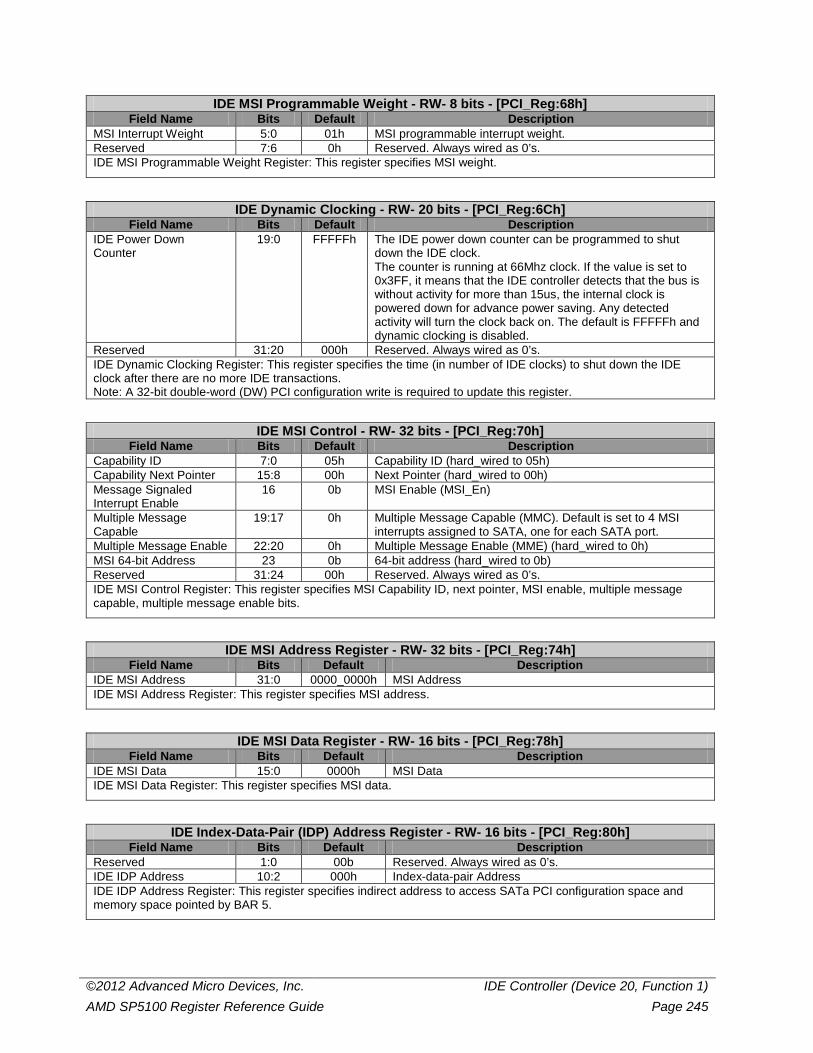
©2012 Advanced Micro Devices, Inc. IDE Controller (Device 20, Function 1) AMD SP5100 Register Reference Guide Page 245
IDE MSI Programmable Weight - RW- 8 bits - [PCI_Reg:68h] Field Name Bits Default Description
MSI Interrupt Weight 5:0 01h MSI programmable interrupt weight. Reserved 7:6 0h Reserved. Always wired as 0’s. IDE MSI Programmable Weight Register: This register specifies MSI weight.
IDE Dynamic Clocking - RW- 20 bits - [PCI_Reg:6Ch] Field Name Bits Default Description
IDE Power Down Counter
19:0 FFFFFh The IDE power down counter can be programmed to shut down the IDE clock. The counter is running at 66Mhz clock. If the value is set to 0x3FF, it means that the IDE controller detects that the bus is without activity for more than 15us, the internal clock is powered down for advance power saving. Any detected activity will turn the clock back on. The default is FFFFFh and dynamic clocking is disabled.
Reserved 31:20 000h Reserved. Always wired as 0’s. IDE Dynamic Clocking Register: This register specifies the time (in number of IDE clocks) to shut down the IDE clock after there are no more IDE transactions. Note: A 32-bit double-word (DW) PCI configuration write is required to update this register.
IDE MSI Control - RW- 32 bits - [PCI_Reg:70h] Field Name Bits Default Description
Capability ID 7:0 05h Capability ID (hard_wired to 05h) Capability Next Pointer 15:8 00h Next Pointer (hard_wired to 00h) Message Signaled Interrupt Enable
16 0b MSI Enable (MSI_En)
Multiple Message Capable
19:17 0h Multiple Message Capable (MMC). Default is set to 4 MSI interrupts assigned to SATA, one for each SATA port.
Multiple Message Enable 22:20 0h Multiple Message Enable (MME) (hard_wired to 0h) MSI 64-bit Address 23 0b 64-bit address (hard_wired to 0b) Reserved 31:24 00h Reserved. Always wired as 0’s. IDE MSI Control Register: This register specifies MSI Capability ID, next pointer, MSI enable, multiple message capable, multiple message enable bits.
IDE MSI Address Register - RW- 32 bits - [PCI_Reg:74h] Field Name Bits Default Description
IDE MSI Address 31:0 0000_0000h MSI Address IDE MSI Address Register: This register specifies MSI address.
IDE MSI Data Register - RW- 16 bits - [PCI_Reg:78h] Field Name Bits Default Description
IDE MSI Data 15:0 0000h MSI Data IDE MSI Data Register: This register specifies MSI data.
IDE Index-Data-Pair (IDP) Address Register - RW- 16 bits - [PCI_Reg:80h] Field Name Bits Default Description
Reserved 1:0 00b Reserved. Always wired as 0’s. IDE IDP Address 10:2 000h Index-data-pair Address IDE IDP Address Register: This register specifies indirect address to access SATa PCI configuration space and memory space pointed by BAR 5.
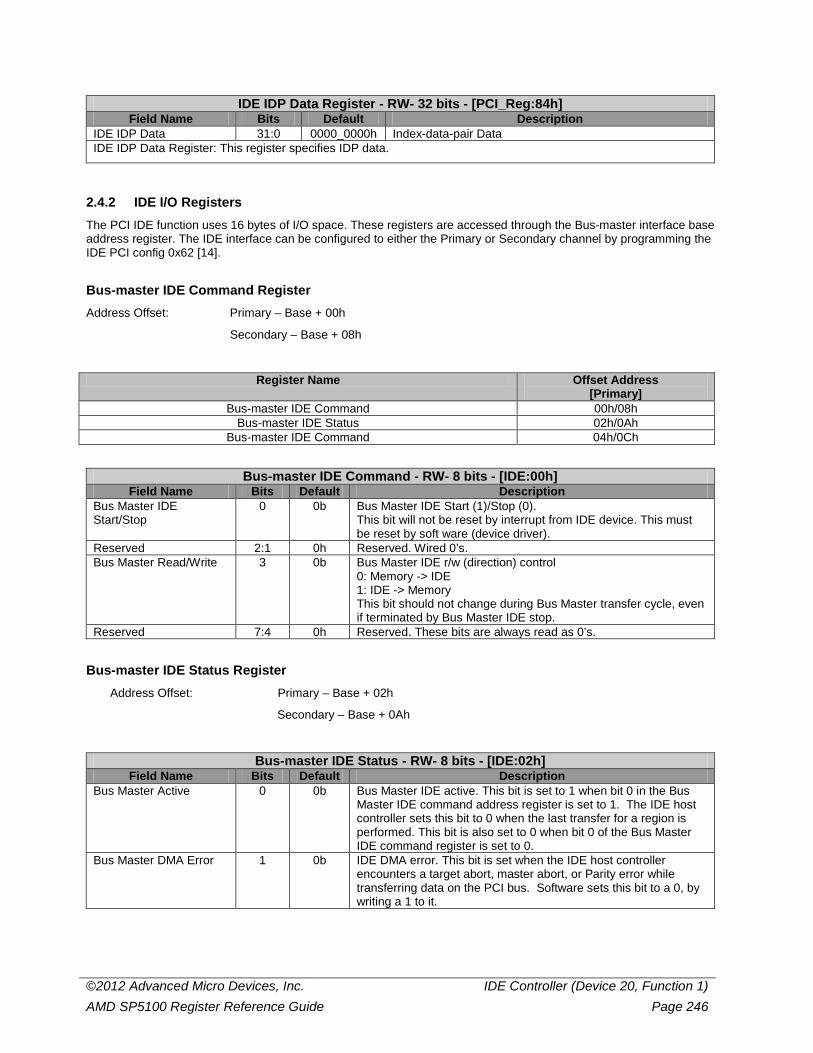
©2012 Advanced Micro Devices, Inc. IDE Controller (Device 20, Function 1) AMD SP5100 Register Reference Guide Page 246
IDE IDP Data Register - RW- 32 bits - [PCI_Reg:84h] Field Name Bits Default Description
IDE IDP Data 31:0 0000_0000h Index-data-pair Data IDE IDP Data Register: This register specifies IDP data.
2.4.2 IDE I/O Registers The PCI IDE function uses 16 bytes of I/O space. These registers are accessed through the Bus-master interface base address register. The IDE interface can be configured to either the Primary or Secondary channel by programming the IDE PCI config 0x62 [14].
Bus-master IDE Command Register Address Offset: Primary – Base + 00h
Secondary – Base + 08h
Register Name Offset Address [Primary]
Bus-master IDE Command 00h/08h Bus-master IDE Status 02h/0Ah
Bus-master IDE Command 04h/0Ch
Bus-master IDE Command - RW- 8 bits - [IDE:00h] Field Name Bits Default Description
Bus Master IDE Start/Stop
0 0b Bus Master IDE Start (1)/Stop (0). This bit will not be reset by interrupt from IDE device. This must be reset by soft ware (device driver).
Reserved 2:1 0h Reserved. Wired 0’s. Bus Master Read/Write 3 0b Bus Master IDE r/w (direction) control
0: Memory -> IDE 1: IDE -> Memory This bit should not change during Bus Master transfer cycle, even if terminated by Bus Master IDE stop.
Reserved 7:4 0h Reserved. These bits are always read as 0’s.
Bus-master IDE Status Register Address Offset: Primary – Base + 02h
Secondary – Base + 0Ah
Bus-master IDE Status - RW- 8 bits - [IDE:02h] Field Name Bits Default Description
Bus Master Active 0 0b Bus Master IDE active. This bit is set to 1 when bit 0 in the Bus Master IDE command address register is set to 1. The IDE host controller sets this bit to 0 when the last transfer for a region is performed. This bit is also set to 0 when bit 0 of the Bus Master IDE command register is set to 0.
Bus Master DMA Error 1 0b IDE DMA error. This bit is set when the IDE host controller encounters a target abort, master abort, or Parity error while transferring data on the PCI bus. Software sets this bit to a 0, by writing a 1 to it.
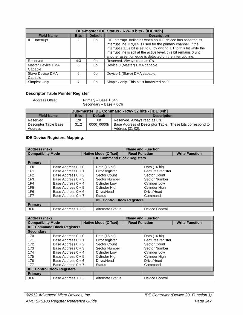
©2012 Advanced Micro Devices, Inc. IDE Controller (Device 20, Function 1) AMD SP5100 Register Reference Guide Page 247
Bus-master IDE Status - RW- 8 bits - [IDE:02h] Field Name Bits Default Description
IDE Interrupt 2 0b IDE Interrupt. Indicates when an IDE device has asserted its interrupt line. IRQ14 is used for the primary channel. If the interrupt status bit is set to 0, by writing a 1 to this bit while the interrupt line is still at the active level, this bit remains 0 until another assertion edge is detected on the interrupt line.
Reserved 4:3 0h Reserved. Always read as 0’s. Master Device DMA Capable
5 0b Device 0 (Master) DMA capable.
Slave Device DMA Capable
6 0b Device 1 (Slave) DMA capable.
Simplex Only 7 0b Simplex only. This bit is hardwired as 0.
Descriptor Table Pointer Register Address Offset: Primary – Base + 04h
Secondary – Base + 0Ch
Bus-master IDE Command - RW- 32 bits - [IDE:04h] Field Name Bits Default Description
Reserved 1:0 0h Reserved. Always read as 0’s. Descriptor Table Base Address
31:2 0000_0000h Base Address of Descriptor Table. These bits correspond to Address [31-02].
IDE Device Registers Mapping:
Address (hex) Name and Function Compatibilty Mode Native Mode (Offset) Read Function Write Function
IDE Command Block Registers Primary 1F0 Base Address 0 + 0 Data (16 bit) Data (16 bit) 1F1 Base Address 0 + 1 Error register Features register 1F2 Base Address 0 + 2 Sector Count Sector Count 1F3 Base Address 0 + 3 Sector Number Sector Number 1F4 Base Address 0 + 4 Cylinder Low Cylinder Low 1F5 Base Address 0 + 5 Cylinder High Cylinder High 1F6 Base Address 0 + 6 Drive/Head Drive/Head 1F7 Base Address 0 + 7 Status Command
IDE Control Block Registers Primary 3F6 Base Address 1 + 2 Alternate Status Device Control
Address (hex) Name and Function Compatibilty Mode Native Mode (Offset) Read Function Write Function IDE Command Block Registers Secondary 170 Base Address 0 + 0 Data (16 bit) Data (16 bit) 171 Base Address 0 + 1 Error register Features register 172 Base Address 0 + 2 Sector Count Sector Count 173 Base Address 0 + 3 Sector Number Sector Number 174 Base Address 0 + 4 Cylinder Low Cylinder Low 175 Base Address 0 + 5 Cylinder High Cylinder High 176 Base Address 0 + 6 Drive/Head Drive/Head 177 Base Address 0 + 7 Status Command IDE Control Block Registers Primary 3F6 Base Address 1 + 2 Alternate Status Device Control
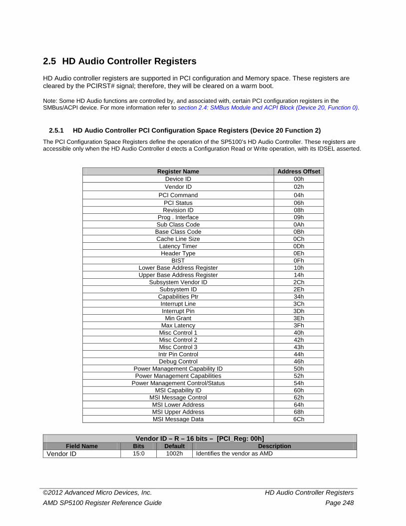
©2012 Advanced Micro Devices, Inc. HD Audio Controller Registers AMD SP5100 Register Reference Guide Page 248
2.5 HD Audio Controller Registers
HD Audio controller registers are supported in PCI configuration and Memory space. These registers are cleared by the PCIRST# signal; therefore, they will be cleared on a warm boot. Note: Some HD Audio functions are controlled by, and associated with, certain PCI configuration registers in the SMBus/ACPI device. For more information refer to section 2.4: SMBus Module and ACPI Block (Device 20, Function 0).
2.5.1 HD Audio Controller PCI Configuration Space Registers (Device 20 Function 2) The PCI Configuration Space Registers define the operation of the SP5100’s HD Audio Controller. These registers are accessible only when the HD Audio Controller d etects a Configuration Read or Write operation, with its IDSEL asserted.
Register Name Address Offset Device ID 00h Vendor ID 02h
PCI Command 04h PCI Status 06h Revision ID 08h
Prog . Interface 09h Sub Class Code 0Ah Base Class Code 0Bh Cache Line Size 0Ch Latency Timer 0Dh Header Type 0Eh
BIST 0Fh Lower Base Address Register 10h Upper Base Address Register 14h
Subsystem Vendor ID 2Ch Subsystem ID 2Eh Capabilities Ptr 34h Interrupt Line 3Ch Interrupt Pin 3Dh Min Grant 3Eh
Max Latency 3Fh Misc Control 1 40h Misc Control 2 42h Misc Control 3 43h Intr Pin Control 44h Debug Control 46h
Power Management Capability ID 50h Power Management Capabilities 52h
Power Management Control/Status 54h MSI Capability ID 60h
MSI Message Control 62h MSI Lower Address 64h MSI Upper Address 68h MSI Message Data 6Ch
Vendor ID – R – 16 bits – [PCI_Reg: 00h] Field Name Bits Default Description
Vendor ID 15:0 1002h Identifies the vendor as AMD
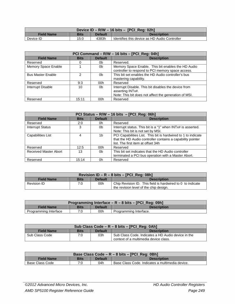
©2012 Advanced Micro Devices, Inc. HD Audio Controller Registers AMD SP5100 Register Reference Guide Page 249
Device ID – R/W – 16 bits – [PCI_Reg: 02h] Field Name Bits Default Description
Device ID 15:0 4383h Identifies this device as HD Audio Controller
PCI Command – R/W – 16 bits – [PCI_Reg: 04h] Field Name Bits Default Description
Reserved 0 0b Reserved. Memory Space Enable 1 0b Memory Space Enable. This bit enables the HD Audio
controller to respond to PCI memory space access. Bus Master Enable 2 0b This bit set enables the HD Audio controller’s bus
mastering capability. Reserved 9:3 00h Reserved Interrupt Disable 10 0b Interrupt Disable. This bit disables the device from
asserting INTx#. Note: This bit does not affect the generation of MSI.
Reserved 15:11 00h Reserved
PCI Status – R/W – 16 bits – [PCI_Reg: 06h] Field Name Bits Default Description
Reserved 2:0 0h Reserved Interrupt Status 3 0b Interrupt status. This bit is a “1” when INTx# is asserted.
Note: This bit is not set by MSI. Capabilities List 4 1b PCI Capabilities List. This bit is hardwired to 1 to indicate
that the HD Audio controller contains a capability pointer list. The first item at offset 34h
Reserved 12:5 00h Reserved Received Master Abort 13 0b This bit set indicates that the HD Audio controller
terminated a PCI bus operation with a Master Abort. Reserved 15:14 0h Reserved
Revision ID – R – 8 bits – [PCI_Reg: 08h] Field Name Bits Default Description
Revision ID 7:0 00h Chip Revision ID. This field is hardwired to 0 to indicate the revision level of the chip design.
Programming Interface – R – 8 bits – [PCI_Reg: 09h] Field Name Bits Default Description
Programming Interface 7:0 00h Programming Interface.
Sub Class Code – R – 8 bits – [PCI_Reg: 0Ah] Field Name Bits Default Description
Sub Class Code 7:0 03h Sub Class Code. Indicates a HD Audio device in the context of a multimedia device class.
Base Class Code – R – 8 bits – [PCI_Reg: 0Bh] Field Name Bits Default Description
Base Class Code 7:0 04h Base Class Code. Indicates a multimedia device.
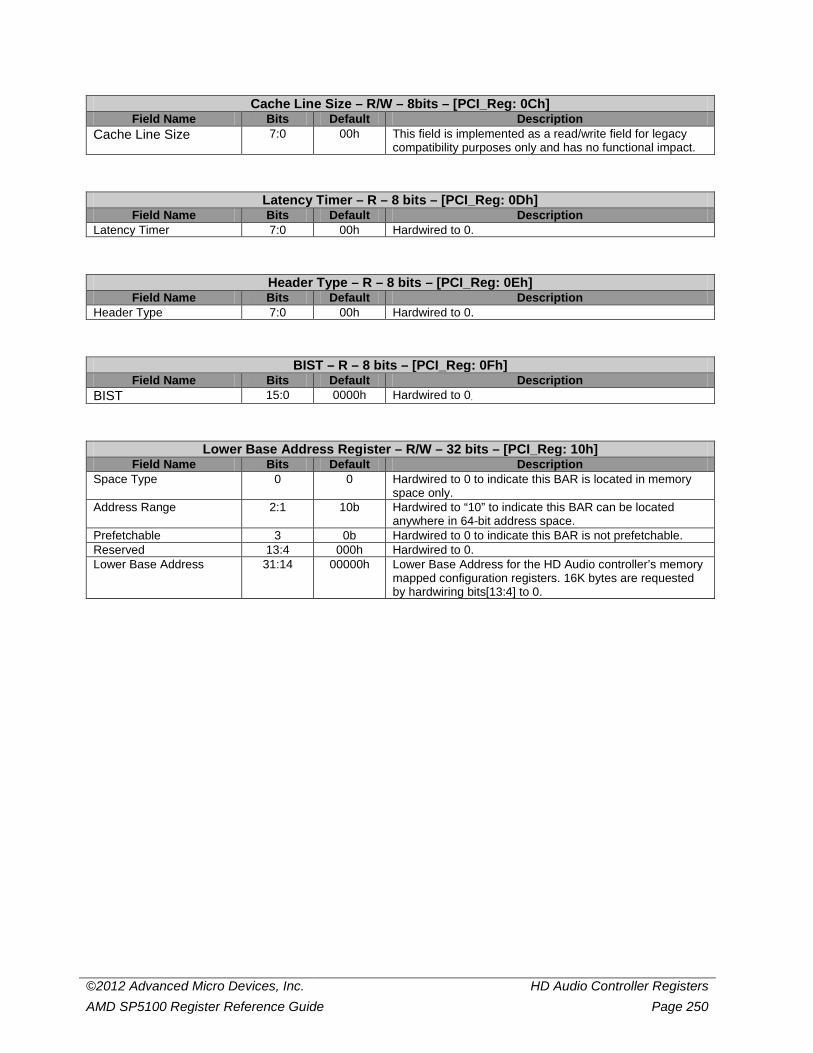
©2012 Advanced Micro Devices, Inc. HD Audio Controller Registers AMD SP5100 Register Reference Guide Page 250
Cache Line Size – R/W – 8bits – [PCI_Reg: 0Ch] Field Name Bits Default Description
Cache Line Size 7:0 00h This field is implemented as a read/write field for legacy compatibility purposes only and has no functional impact.
Latency Timer – R – 8 bits – [PCI_Reg: 0Dh] Field Name Bits Default Description
Latency Timer 7:0 00h Hardwired to 0.
Header Type – R – 8 bits – [PCI_Reg: 0Eh] Field Name Bits Default Description
Header Type 7:0 00h Hardwired to 0.
BIST – R – 8 bits – [PCI_Reg: 0Fh] Field Name Bits Default Description
BIST 15:0 0000h Hardwired to 0.
Lower Base Address Register – R/W – 32 bits – [PCI_Reg: 10h] Field Name Bits Default Description
Space Type 0 0 Hardwired to 0 to indicate this BAR is located in memory space only.
Address Range 2:1 10b Hardwired to “10” to indicate this BAR can be located anywhere in 64-bit address space.
Prefetchable 3 0b Hardwired to 0 to indicate this BAR is not prefetchable. Reserved 13:4 000h Hardwired to 0. Lower Base Address 31:14 00000h Lower Base Address for the HD Audio controller’s memory
mapped configuration registers. 16K bytes are requested by hardwiring bits[13:4] to 0.
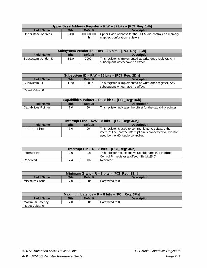
©2012 Advanced Micro Devices, Inc. HD Audio Controller Registers AMD SP5100 Register Reference Guide Page 251
Upper Base Address Register – R/W – 32 bits – [PCI_Reg: 14h] Field Name Bits Default Description
Upper Base Address 31:0 00000000h
Upper Base Address for the HD Audio controller’s memory mapped confuration registers.
Subsystem Vendor ID – R/W – 16 bits – [PCI_Reg: 2Ch] Field Name Bits Default Description
Subsystem Vendor ID 15:0 0000h This register is implemented as write-once register. Any subsequent writes have no effect.
Subsystem ID – R/W – 16 bits – [PCI_Reg: 2Dh] Field Name Bits Default Description
Subsystem ID 15:0 0000h This register is implemented as write-once register. Any subsequent writes have no effect.
Reset Value: 0
Capabilities Pointer – R – 8 bits – [PCI_Reg: 34h] Field Name Bits Default Description
Capabilities Pointer 7:0 50h This register indicates the offset for the capability pointer
Interrupt Line – R/W – 8 bits – [PCI_Reg: 3Ch] Field Name Bits Default Description
Interrupt Line 7:0 00h This register is used to communicate to software the interrupt line that the interrupt pin is connected to. It is not used by the HD Audio controller.
Interrupt Pin – R – 8 bits – [PCI_Reg: 3Dh] Interrupt Pin 3:0 1h This register reflects the value programs into Interrupt
Control Pin register at offset 44h, bits[3:0] Reserved 7:4 0h Reserved
Minimum Grant – R – 8 bits – [PCI_Reg: 3Eh] Field Name Bits Default Description
Minimum Grant 7:0 00h Hardwired to 0.
Maximum Latency – R – 8 bits – [PCI_Reg: 3Fh] Field Name Bits Default Description
Maximum Latency 7:0 00h Hardwired to 0. Reset Value: 0
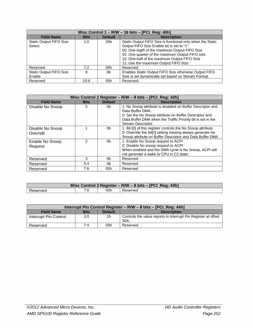
©2012 Advanced Micro Devices, Inc. HD Audio Controller Registers AMD SP5100 Register Reference Guide Page 252
Misc Control 1 – R/W – 16 bits – [PCI_Reg: 40h] Field Name Bits Default Description
Static Output FIFO Size Select
1:0 00b Static Output FIFO Size is functional only when the Static Output FIFO Size Enable bit is set to “1”. 00: One-eigth of the maximum Output FIFO Size 01: One-quarter of the maximum Output FIFO size 10: One-half of the maximum Output FIFO Size 11: Use the maximum Output FIFO Size
Reserved 7:2 00h Reserved Static Output FIFO Size Enable
8 0b Enables Static Output FIFO Size otherwise Output FIFO Size is set dynamically set based on Stream Format.
Reserved 15:9 00h Reserved.
Misc Control 2 Register – R/W – 8 bits – [PCI_Reg: 42h] Field Name Bits Default Description
Disable No Snoop 0 0b 1: No Snoop attribute is disabled on Buffer Descriptor and Data Buffer DMA. 0: Set the No Snoop attribute on Buffer Descriptor and Data Buffer DMA when the Traffic Priority bit is set in the Stream Descriptor.
Disable No Snoop Override
1 0b 1: Bit [0] of this register controls the No Snoop attribute 0: Override the bit[0] setting meaing always generate No Snoop attribute on Buffer Descriptor and Data Buffer DMA
Enable No Snoop Request
2 0b 1: Enable No Snoop request to ACPI 0: Disable No snoop request to ACPI When enabled and the DMA cycle is No Snoop, ACPI will not generate a wake to CPU in C2 state.
Reserved 3 0b Reserved Reserved 5:4 0b Reserved Reserved 7:6 00h Reserved
Misc Control 3 Register – R/W – 8 bits – [PCI_Reg: 43h] Reserved 7:0 00h Reserved
Interrupt Pin Control Register – R/W – 8 bits – [PCI_Reg: 44h] Field Name Bits Default Description
Interrupt Pin Control 3:0 1h Controls the value reports in Interrupt Pin Register at offset 3Dh.
Reserved 7:4 00h Reserved
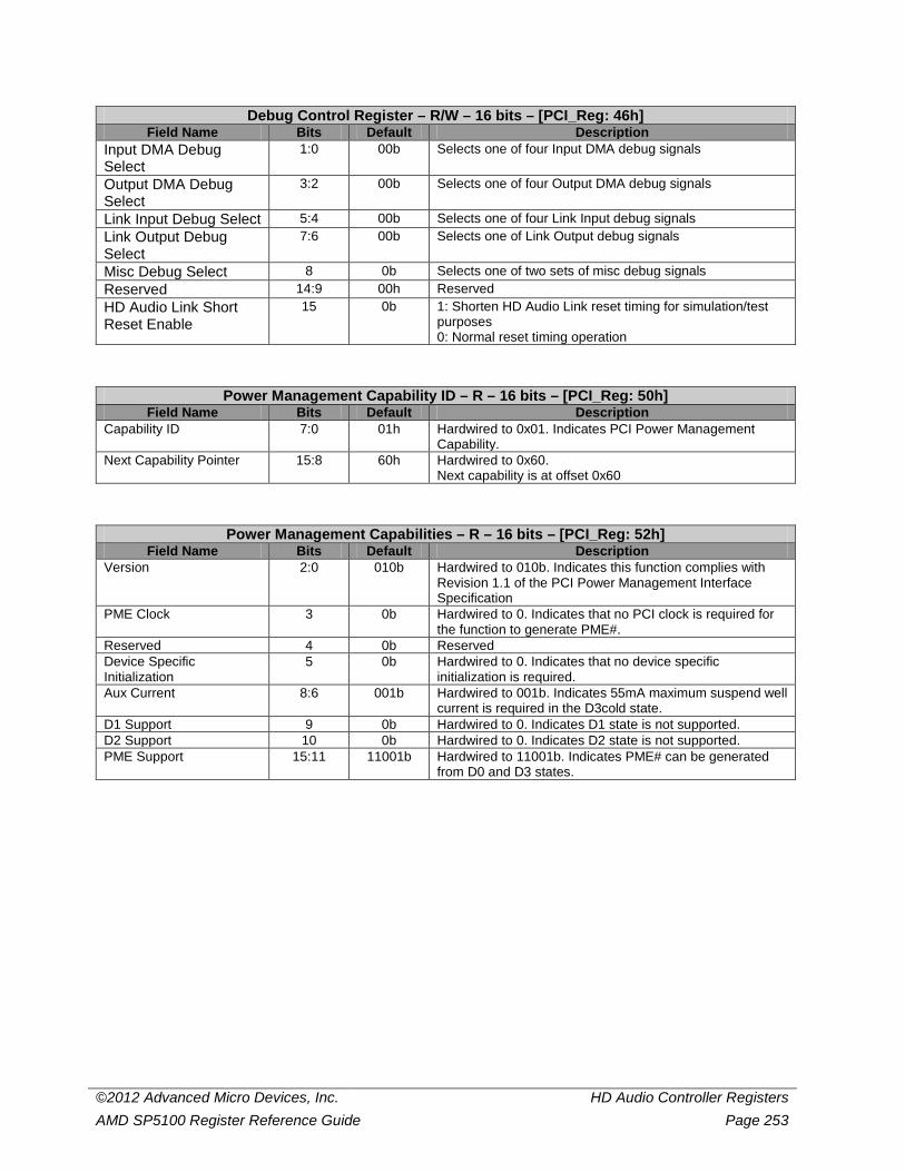
©2012 Advanced Micro Devices, Inc. HD Audio Controller Registers AMD SP5100 Register Reference Guide Page 253
Debug Control Register – R/W – 16 bits – [PCI_Reg: 46h] Field Name Bits Default Description
Input DMA Debug Select
1:0 00b Selects one of four Input DMA debug signals
Output DMA Debug Select
3:2 00b Selects one of four Output DMA debug signals
Link Input Debug Select 5:4 00b Selects one of four Link Input debug signals Link Output Debug Select
7:6 00b Selects one of Link Output debug signals
Misc Debug Select 8 0b Selects one of two sets of misc debug signals Reserved 14:9 00h Reserved HD Audio Link Short Reset Enable
15 0b 1: Shorten HD Audio Link reset timing for simulation/test purposes 0: Normal reset timing operation
Power Management Capability ID – R – 16 bits – [PCI_Reg: 50h] Field Name Bits Default Description
Capability ID 7:0 01h Hardwired to 0x01. Indicates PCI Power Management Capability.
Next Capability Pointer 15:8 60h Hardwired to 0x60. Next capability is at offset 0x60
Power Management Capabilities – R – 16 bits – [PCI_Reg: 52h] Field Name Bits Default Description
Version 2:0 010b Hardwired to 010b. Indicates this function complies with Revision 1.1 of the PCI Power Management Interface Specification
PME Clock 3 0b Hardwired to 0. Indicates that no PCI clock is required for the function to generate PME#.
Reserved 4 0b Reserved Device Specific Initialization
5 0b Hardwired to 0. Indicates that no device specific initialization is required.
Aux Current 8:6 001b Hardwired to 001b. Indicates 55mA maximum suspend well current is required in the D3cold state.
D1 Support 9 0b Hardwired to 0. Indicates D1 state is not supported. D2 Support 10 0b Hardwired to 0. Indicates D2 state is not supported. PME Support 15:11 11001b Hardwired to 11001b. Indicates PME# can be generated
from D0 and D3 states.
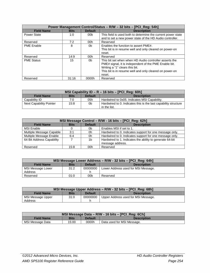
©2012 Advanced Micro Devices, Inc. HD Audio Controller Registers AMD SP5100 Register Reference Guide Page 254
Power Management Control/Status – R/W – 32 bits – [PCI_Reg: 54h] Field Name Bits Default Description
Power State 1:0 00b This field is used both to determine the current power state and to set a new power state of the HD Audio controller.
Reserved 7:2 00h Reserved PME Enable 8 0b Enables the function to assert PME#.
This bit is in resume well and only cleared on power-on reset.
Reserved 14:9 00h Reserved PME Status 15 0b This bit set when when HD Audio controller asserts the
PME# signal, it is independent of the PME Enable bit. Writing a “1” clears this bit. This bit is in resume well and only cleared on power-on reset.
Reserved 31:16 0000h Reserved
MSI Capability ID – R – 16 bits – [PCI_Reg: 60h] Field Name Bits Default Description
Capability ID 7:0 05h Hardwired to 0x05. Indicates MSI Capability. Next Capability Pointer 15:8 0b Hardwired to 0. Indicates this is the last capability structure
in the list.
MSI Message Control – R/W - 16 bits – [PCI_Reg: 62h] Field Name Bits Default Description
MSI Enable 0 0b Enables MSI if set to 1. Multiple Message Capable 3:1 0h Hardwired to 0. Indicates support for one message only. Multiple Message Enable 6:4 0h Hardwired to 0. Indicates support for one message only. 64 Bit Address Capability 7 1b Hardwired to 1. Indicates the ability to generate 64-bit
message address. Reserved 15:8 00h Reserved
MSI Message Lower Address – R/W - 32 bits – [PCI_Reg: 64h] Field Name Bits Default Description
MSI Message Lower Address
31:2 00000000h
Lower Address used for MSI Message.
Reserved 01:0 00b Reserved
MSI Message Upper Address – R/W - 32 bits – [PCI_Reg: 68h] Field Name Bits Default Description
MSI Message Upper Address
31:0 00000000h
Upper Address used for MSI Message.
MSI Message Data – R/W - 16 bits – [PCI_Reg: 6Ch] Field Name Bits Default Description
MSI Message Data 15:00 0000h Data used for MSI Message.
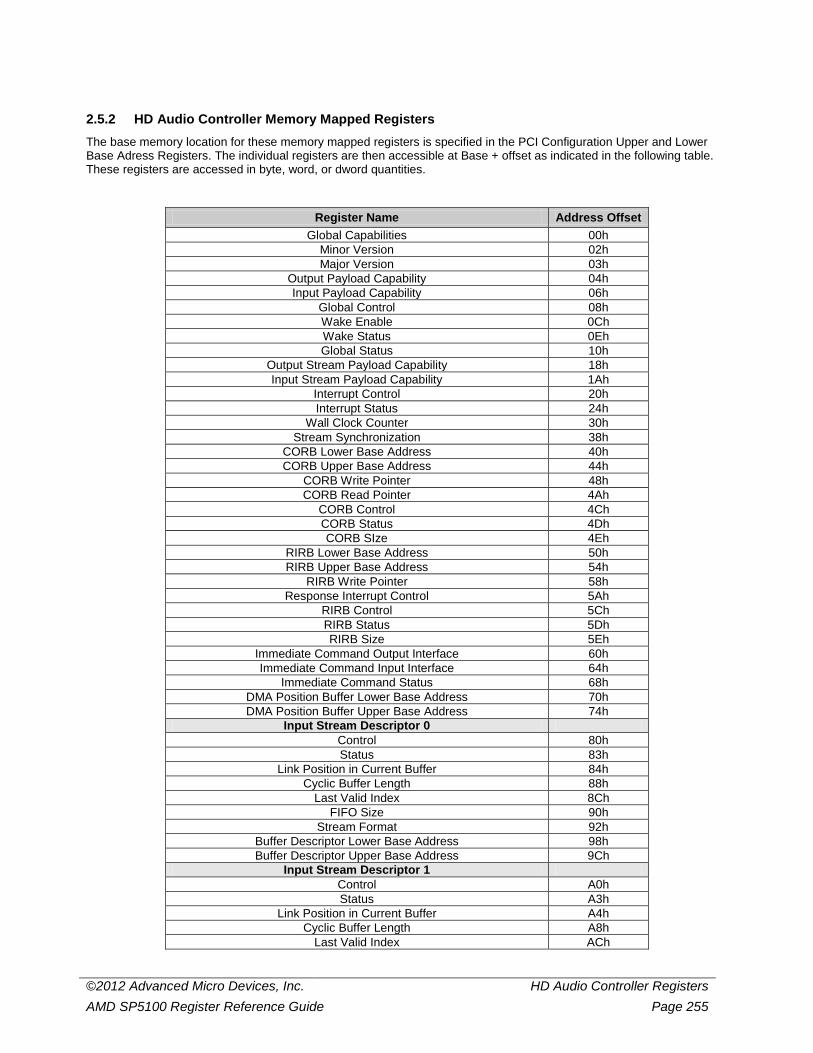
©2012 Advanced Micro Devices, Inc. HD Audio Controller Registers AMD SP5100 Register Reference Guide Page 255
2.5.2 HD Audio Controller Memory Mapped Registers The base memory location for these memory mapped registers is specified in the PCI Configuration Upper and Lower Base Adress Registers. The individual registers are then accessible at Base + offset as indicated in the following table. These registers are accessed in byte, word, or dword quantities.
Register Name Address Offset Global Capabilities 00h
Minor Version 02h Major Version 03h
Output Payload Capability 04h Input Payload Capability 06h
Global Control 08h Wake Enable 0Ch Wake Status 0Eh Global Status 10h
Output Stream Payload Capability 18h Input Stream Payload Capability 1Ah
Interrupt Control 20h Interrupt Status 24h
Wall Clock Counter 30h Stream Synchronization 38h
CORB Lower Base Address 40h CORB Upper Base Address 44h
CORB Write Pointer 48h CORB Read Pointer 4Ah
CORB Control 4Ch CORB Status 4Dh CORB SIze 4Eh
RIRB Lower Base Address 50h RIRB Upper Base Address 54h
RIRB Write Pointer 58h Response Interrupt Control 5Ah
RIRB Control 5Ch RIRB Status 5Dh RIRB Size 5Eh
Immediate Command Output Interface 60h Immediate Command Input Interface 64h
Immediate Command Status 68h DMA Position Buffer Lower Base Address 70h DMA Position Buffer Upper Base Address 74h
Input Stream Descriptor 0 Control 80h Status 83h
Link Position in Current Buffer 84h Cyclic Buffer Length 88h
Last Valid Index 8Ch FIFO Size 90h
Stream Format 92h Buffer Descriptor Lower Base Address 98h Buffer Descriptor Upper Base Address 9Ch
Input Stream Descriptor 1 Control A0h Status A3h
Link Position in Current Buffer A4h Cyclic Buffer Length A8h
Last Valid Index ACh

©2012 Advanced Micro Devices, Inc. HD Audio Controller Registers AMD SP5100 Register Reference Guide Page 256
Register Name Address Offset FIFO Size B0h
Stream Format B2h Buffer Descriptor Lower Base Address B8h Buffer Descriptor Upper Base Address BCh
Input Stream Descriptor 2 Control C0h Status C3h
Link Position in Current Buffer C4h Cyclic Buffer Length C8h
Last Valid Index CCh FIFO Size D0h
Stream Format D2h Buffer Descriptor Lower Base Address D8h Buffer Descriptor Upper Base Address DCh
Input Stream Descriptor 3 Control E0h Status E3h
Link Position in Current Buffer E4h Cyclic Buffer Length E8h
Last Valid Index ECh FIFO Size F0h
Stream Format F2h Buffer Descriptor Lower Base Address F8h Buffer Descriptor Upper Base Address FCh
Output Stream Descriptor 0 Control 100h Status 103h
Link Position in Current Buffer 104h Cyclic Buffer Length 108h
Last Valid Index 10Ch FIFO Size 110h
Stream Format 112h Buffer Descriptor Lower Base Address 118h Buffer Descriptor Upper Base Address 11Ch
Output Stream Descriptor 1 Control 120h Status 123h
Link Position in Current Buffer 124h Cyclic Buffer Length 128h
Last Valid Index 12Ch FIFO Size 130h
Stream Format 132h Buffer Descriptor Lower Base Address 138h Buffer Descriptor Upper Base Address 13Ch
Output Stream Descriptor 2 Control 140h Status 143h
Link Position in Current Buffer 144h Cyclic Buffer Length 148h
Last Valid Index 14Ch FIFO Size 150h
Stream Format 152h Buffer Descriptor Lower Base Address 158h Buffer Descriptor Upper Base Address 15Ch
Output Stream Descriptor 3 Control 160h Status 163h
Link Position in Current Buffer 164h
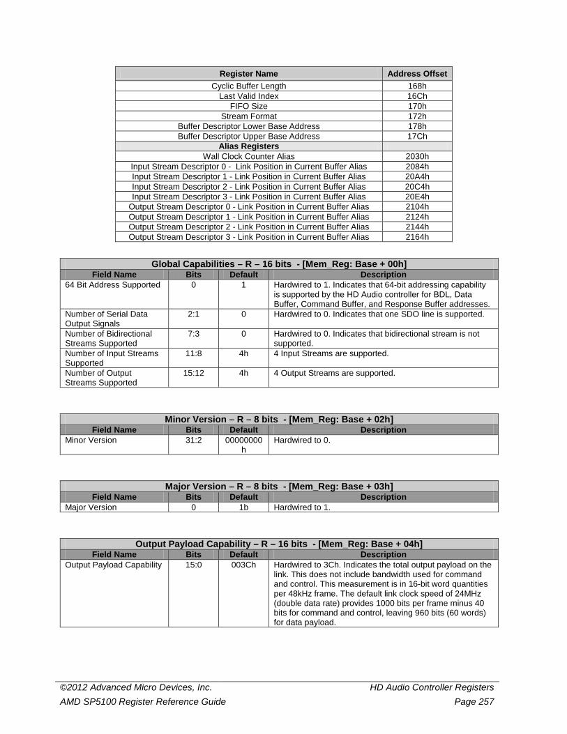
©2012 Advanced Micro Devices, Inc. HD Audio Controller Registers AMD SP5100 Register Reference Guide Page 257
Register Name Address Offset Cyclic Buffer Length 168h
Last Valid Index 16Ch FIFO Size 170h
Stream Format 172h Buffer Descriptor Lower Base Address 178h Buffer Descriptor Upper Base Address 17Ch
Alias Registers Wall Clock Counter Alias 2030h
Input Stream Descriptor 0 - Link Position in Current Buffer Alias 2084h Input Stream Descriptor 1 - Link Position in Current Buffer Alias 20A4h Input Stream Descriptor 2 - Link Position in Current Buffer Alias 20C4h Input Stream Descriptor 3 - Link Position in Current Buffer Alias 20E4h
Output Stream Descriptor 0 - Link Position in Current Buffer Alias 2104h Output Stream Descriptor 1 - Link Position in Current Buffer Alias 2124h Output Stream Descriptor 2 - Link Position in Current Buffer Alias 2144h Output Stream Descriptor 3 - Link Position in Current Buffer Alias 2164h
Global Capabilities – R – 16 bits - [Mem_Reg: Base + 00h] Field Name Bits Default Description
64 Bit Address Supported 0 1 Hardwired to 1. Indicates that 64-bit addressing capability is supported by the HD Audio controller for BDL, Data Buffer, Command Buffer, and Response Buffer addresses.
Number of Serial Data Output Signals
2:1 0 Hardwired to 0. Indicates that one SDO line is supported.
Number of Bidirectional Streams Supported
7:3 0 Hardwired to 0. Indicates that bidirectional stream is not supported.
Number of Input Streams Supported
11:8 4h 4 Input Streams are supported.
Number of Output Streams Supported
15:12 4h 4 Output Streams are supported.
Minor Version – R – 8 bits - [Mem_Reg: Base + 02h] Field Name Bits Default Description
Minor Version 31:2 00000000h
Hardwired to 0.
Major Version – R – 8 bits - [Mem_Reg: Base + 03h] Field Name Bits Default Description
Major Version 0 1b Hardwired to 1.
Output Payload Capability – R – 16 bits - [Mem_Reg: Base + 04h] Field Name Bits Default Description
Output Payload Capability 15:0 003Ch Hardwired to 3Ch. Indicates the total output payload on the link. This does not include bandwidth used for command and control. This measurement is in 16-bit word quantities per 48kHz frame. The default link clock speed of 24MHz (double data rate) provides 1000 bits per frame minus 40 bits for command and control, leaving 960 bits (60 words) for data payload.
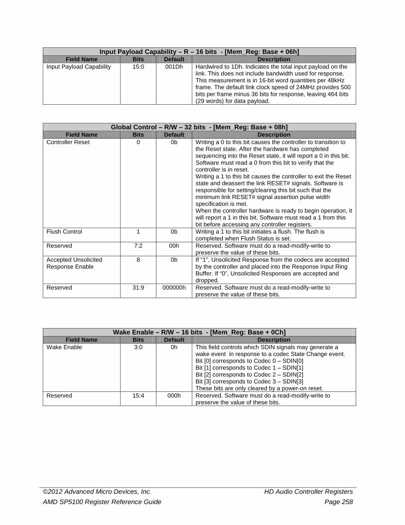
©2012 Advanced Micro Devices, Inc. HD Audio Controller Registers AMD SP5100 Register Reference Guide Page 258
Input Payload Capability – R – 16 bits - [Mem_Reg: Base + 06h] Field Name Bits Default Description
Input Payload Capability 15:0 001Dh Hardwired to 1Dh. Indicates the total input payload on the link. This does not include bandwidth used for response. This measurement is in 16-bit word quantities per 48kHz frame. The default link clock speed of 24MHz provides 500 bits per frame minus 36 bits for response, leaving 464 bits (29 words) for data payload.
Global Control – R/W – 32 bits - [Mem_Reg: Base + 08h] Field Name Bits Default Description
Controller Reset 0 0b Writing a 0 to this bit causes the controller to transition to the Reset state. After the hardware has completed sequencing into the Reset state, it will report a 0 in this bit. Software must read a 0 from this bit to verify that the controller is in reset. Writing a 1 to this bit causes the controller to exit the Reset state and deassert the link RESET# signals. Software is responsible for setting/clearing this bit such that the minimum link RESET# signal assertion pulse width specification is met. When the controller hardware is ready to begin operation, it will report a 1 in this bit. Software must read a 1 from this bit before accessing any controller registers.
Flush Control 1 0b Writing a 1 to this bit initiates a flush. The flush is completed when Flush Status is set.
Reserved 7:2 00h Reserved. Software must do a read-modify-write to preserve the value of these bits.
Accepted Unsolicited Response Enable
8 0b If “1”, Unsolicited Response from the codecs are accepted by the controller and placed into the Response Input Ring Buffer. If “0”, Unsolicited Responses are accepted and dropped.
Reserved 31:9 000000h Reserved. Software must do a read-modify-write to preserve the value of these bits.
Wake Enable – R/W – 16 bits - [Mem_Reg: Base + 0Ch] Field Name Bits Default Description
Wake Enable 3:0 0h This field controls which SDIN signals may generate a wake event in response to a codec State Change event. Bit [0] corresponds to Codec 0 – SDIN[0] Bit [1] corresponds to Codec 1 – SDIN[1] Bit [2] corresponds to Codec 2 – SDIN[2] Bit [3] corresponds to Codec 3 – SDIN[3] These bits are only cleared by a power-on reset.
Reserved 15:4 000h Reserved. Software must do a read-modify-write to preserve the value of these bits.
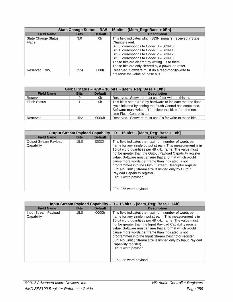
©2012 Advanced Micro Devices, Inc. HD Audio Controller Registers AMD SP5100 Register Reference Guide Page 259
State Change Status – R/W – 16 bits - [Mem_Reg: Base + 0Eh] Field Name Bits Default Description
State Change Status Flags
3:0 0h This field indicates which SDIN signal(s) received a State Change event. Bit [0] corresponds to Codec 0 – SDIN[0] Bit [1] corresponds to Codec 1 – SDIN[1] Bit [2] corresponds to Codec 2 – SDIN[2] Bit [3] corresponds to Codec 3 – SDIN[3] These bits are cleared by writing 1’s to them. These bits are only cleared by a power-on reset.
Reserved (R/W) 15:4 000h Reserved. Software must do a read-modify-write to preserve the value of these bits.
Global Status – R/W – 16 bits - [Mem_Reg: Base + 10h] Field Name Bits Default Description
Reserved 0 0b Reserved. Software must use 0 for write to this bit. Flush Status 1 0b This bit is set to a “1” by hardware to indicate that the flush
cycle initiated by setting the Flush Control has completed. Software must write a “1” to clear this bit before the next time Flush Control is set.
Reserved 15:2 0000h Reserved. Software must use 0’s for write to these bits.
Output Stream Payload Capability – R – 16 bits - [Mem_Reg: Base + 18h] Field Name Bits Default Description
Output Stream Payload Capability
15:0 003Ch This field indicates the maximum number of words per frame for any single output stream. This measurement is in 16-bit word quantities per 48 kHz frame. The value must not be greater than the Output Payload Capability register value. Software must ensure that a format which would cause more words per frame than indicated is not programmed into the Output Stream Descriptor register. 00h: No Limit ( Stream size is limited only by Output Payload Capability register) 01h: 1 word payload : : FFh: 255 word payload
Input Stream Payload Capability – R – 16 bits - [Mem_Reg: Base + 1Ah] Field Name Bits Default Description
Input Stream Payload Capability
15:0 0000h This field indicates the maximum number of words per frame for any single input stream. This measurement is in 16-bit word quantities per 48 kHz frame. The value must not be greater than the Input Payload Capability register value. Software must ensure that a format which would cause more words per frame than indicated is not programmed into the Input Stream Descriptor register. 00h: No Limit ( Stream size is limited only by Input Payload Capability register) 01h: 1 word payload : : FFh: 255 word payload
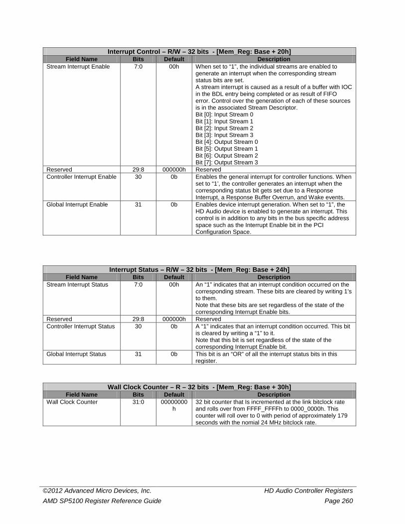
©2012 Advanced Micro Devices, Inc. HD Audio Controller Registers AMD SP5100 Register Reference Guide Page 260
Interrupt Control – R/W – 32 bits - [Mem_Reg: Base + 20h] Field Name Bits Default Description
Stream Interrupt Enable 7:0 00h When set to “1”, the individual streams are enabled to generate an interrupt when the corresponding stream status bits are set. A stream interrupt is caused as a result of a buffer with IOC in the BDL entry being completed or as result of FIFO error. Control over the generation of each of these sources is in the associated Stream Descriptor. Bit [0]: Input Stream 0 Bit [1]: Input Stream 1 Bit [2]: Input Stream 2 Bit [3]: Input Stream 3 Bit [4]: Output Stream 0 Bit [5]: Output Stream 1 Bit [6]: Output Stream 2 Bit [7]: Output Stream 3
Reserved 29:8 000000h Reserved Controller Interrupt Enable 30 0b Enables the general interrupt for controller functions. When
set to “1’, the controller generates an interrupt when the corresponding status bit gets set due to a Response Interrupt, a Response Buffer Overrun, and Wake events.
Global Interrupt Enable 31 0b Enables device interrupt generation. When set to “1”, the HD Audio device is enabled to generate an interrupt. This control is in addition to any bits in the bus specific address space such as the Interrupt Enable bit in the PCI Configuration Space.
Interrupt Status – R/W – 32 bits - [Mem_Reg: Base + 24h] Field Name Bits Default Description
Stream Interrupt Status 7:0 00h An “1” indicates that an interrupt condition occurred on the corresponding stream. These bits are cleared by writing 1’s to them. Note that these bits are set regardless of the state of the corresponding Interrupt Enable bits.
Reserved 29:8 000000h Reserved Controller Interrupt Status 30 0b A “1” indicates that an interrupt condition occurred. This bit
is cleared by writing a “1” to it. Note that this bit is set regardless of the state of the corresponding Interrupt Enable bit.
Global Interrupt Status 31 0b This bit is an “OR” of all the interrupt status bits in this register.
Wall Clock Counter – R – 32 bits - [Mem_Reg: Base + 30h] Field Name Bits Default Description
Wall Clock Counter 31:0 00000000h
32 bit counter that Is incremented at the link bitclock rate and rolls over from FFFF_FFFFh to 0000_0000h. This counter will roll over to 0 with period of approximately 179 seconds with the nomial 24 MHz bitclock rate.

©2012 Advanced Micro Devices, Inc. HD Audio Controller Registers AMD SP5100 Register Reference Guide Page 261
Stream Synchronization – R/W – 32 bits – [Mem_Reg: Base + 38h] Field Name Bits Default Description
Stream Synchronization 7:0 00h These bits when set, block data from being sent on or received from the link. Each bit controls the associated Stream Descriptor. To synchronously start a set of DMA engines, the bits in this register are set to a “1”. The RUN bits for the associated Stream Descriptors can be set to a “1” to start the DMA engines. When all streams are ready, the associated Stream Synchronization bits can all be set to 0 at the same time, and transmission or reception from the link will begin together at the start of the next full link frame. To synchronously stop streams, these bits are set, and the RUN bits in the Stream Descriptors are cleared by software.
Reserved 31:8 000000h Reserved. Software must do a read-modify-write to preserve the value of these bits.
CORB Lower Base Address – R/W – 32 bits – [Mem_Reg: Base + 40h] Field Name Bits Default Description
CORB Lower Base Address Unimplemented Bits
6:0 00h Hardwired to 0. This forces 128-byte buffer alignment for cache line fetch optimizations.
CORB Lower Base Address
31:7 0000000h Upper 25 bits of the 32 bits Lower Base address of the Command Output Ring Buffer, allowing the CORB Base Address to be assigned on any 1 KB boundary. This register must not be written when the DMA engine is running or the DMA transfer may be corrupted.
CORB Upper Base Address – RW – 32 bits – [Mem_Reg: Base + 44h] Field Name Bits Default Description
CORB Upper Base Address
31:0 00000000h
Upper 32 bits address of the CORB. This register must not be written when the DMA engine is running or the DMA transfer may be corrupted.
CORB Write Pointer – R/W – 16 bits – [Mem_Reg: Base + 48h] Field Name Bits Default Description
CORB Write Pointer 7:0 00h Software writes the last valid CORB entry offset into this field in dword granularity. The DMA engine fetches commands from the CORB until the Read Pointer matches the Write Pointer. This supports up to 256 CORB entries. This field may not be written while the DMA engine is running.
Reserved 15:8 00h Reserved. Software must do a read-modify-write to preserve the value of these bits.
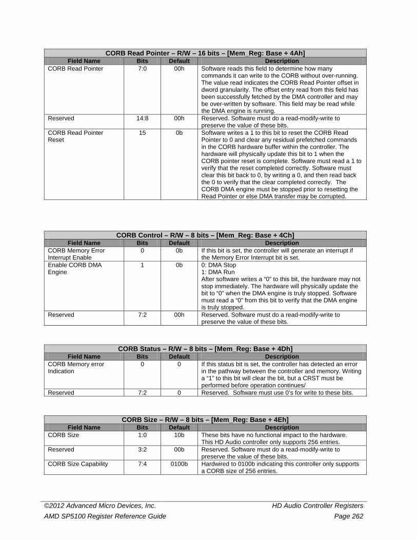
©2012 Advanced Micro Devices, Inc. HD Audio Controller Registers AMD SP5100 Register Reference Guide Page 262
CORB Read Pointer – R/W – 16 bits – [Mem_Reg: Base + 4Ah] Field Name Bits Default Description
CORB Read Pointer 7:0 00h Software reads this field to determine how many commands it can write to the CORB without over-running. The value read indicates the CORB Read Pointer offset in dword granularity. The offset entry read from this field has been successfully fetched by the DMA controller and may be over-written by software. This field may be read while the DMA engine is running.
Reserved 14:8 00h Reserved. Software must do a read-modify-write to preserve the value of these bits.
CORB Read Pointer Reset
15 0b Software writes a 1 to this bit to reset the CORB Read Pointer to 0 and clear any residual prefetched commands in the CORB hardware buffer within the controller. The hardware will physically update this bit to 1 when the CORB pointer reset is complete. Software must read a 1 to verify that the reset completed correctly. Software must clear this bit back to 0, by writing a 0, and then read back the 0 to verify that the clear completed correctly. The CORB DMA engine must be stopped prior to resetting the Read Pointer or else DMA transfer may be corrupted.
CORB Control – R/W – 8 bits – [Mem_Reg: Base + 4Ch] Field Name Bits Default Description
CORB Memory Error Interrupt Enable
0 0b If this bit is set, the controller will generate an interrupt if the Memory Error Interrupt bit is set.
Enable CORB DMA Engine
1 0b 0: DMA Stop 1: DMA Run After software writes a “0” to this bit, the hardware may not stop immediately. The hardware will physically update the bit to “0” when the DMA engine is truly stopped. Software must read a “0” from this bit to verify that the DMA engine is truly stopped.
Reserved 7:2 00h Reserved. Software must do a read-modify-write to preserve the value of these bits.
CORB Status – R/W – 8 bits – [Mem_Reg: Base + 4Dh] Field Name Bits Default Description
CORB Memory error Indication
0 0 If this status bit is set, the controller has detected an error in the pathway between the controller and memory. Writing a “1” to this bit will clear the bit, but a CRST must be performed before operation continues/
Reserved 7:2 0 Reserved. Software must use 0’s for write to these bits.
CORB Size – R/W – 8 bits – [Mem_Reg: Base + 4Eh] Field Name Bits Default Description
CORB Size 1:0 10b These bits have no functional impact to the hardware. This HD Audio controller only supports 256 entries.
Reserved 3:2 00b Reserved. Software must do a read-modify-write to preserve the value of these bits.
CORB Size Capability 7:4 0100b Hardwired to 0100b indicating this controller only supports a CORB size of 256 entries.
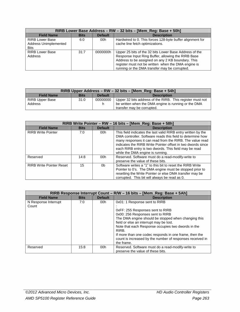
©2012 Advanced Micro Devices, Inc. HD Audio Controller Registers AMD SP5100 Register Reference Guide Page 263
RIRB Lower Base Address – RW – 32 bits – [Mem_Reg: Base + 50h] Field Name Bits Default Description
RIRB Lower Base Address Unimplemented Bits
6:0 00h Hardwired to 0. This forces 128-byte buffer alignment for cache line fetch optimizations.
RIRB Lower Base Address
31:7 0000000h Upper 25 bits of the 32 bits Lower Base Address of the Response Input Ring Buffer, allowing the RIRB Base Address to be assigned on any 2 KB boundary. This register must not be written when the DMA engine is running or the DMA transfer may be corrupted.
RIRB Upper Address – RW – 32 bits – [Mem_Reg: Base + 54h] Field Name Bits Default Description
RIRB Upper Base Address
31:0 00000000h
Upper 32 bits address of the RIRB. This register must not be written when the DMA engine is running or the DMA transfer may be corrupted.
RIRB Write Pointer – RW – 16 bits – [Mem_Reg: Base + 58h] Field Name Bits Default Description
RIRB Write Pointer 7:0 00h This field indicates the last valid RIRB entry written by the DMA controller. Software reads this field to determine how many responses it can read from the RIRB. The value read indicates the RIRB Write Pointer offset in two dwords since each RIRB entry is two dwords. This field may be read while the DMA engine is running.
Reserved 14:8 00h Reserved. Software must do a read-modify-write to preserve the value of these bits.
RIRB Write Pointer Reset 15 0b Software writes a “1” to this bit to reset the RIRB Write Pointer to 0’s. The DMA engine must be stopped prior to resetting the Write Pointer or else DMA transfer may be corrupted. This bit will always be read as 0.
RIRB Response Interrupt Count – R/W – 16 bits – [Mem_Reg: Base + 5Ah] Field Name Bits Default Description
N Response Interrupt Count
7:0 00h 0x01: 1 Response sent to RIRB : 0xFF: 255 Responses sent to RIRB 0x00: 256 Responses sent to RIRB The DMA engine should be stopped when changing this field or else an interrupt may be lost. Note that each Response occupies two dwords in the RIRB. If more than one codec responds in one frame, then the count is increased by the number of responses received in the frame.
Reserved 15:8 00h Reserved. Software must do a read-modify-write to preserve the value of these bits.
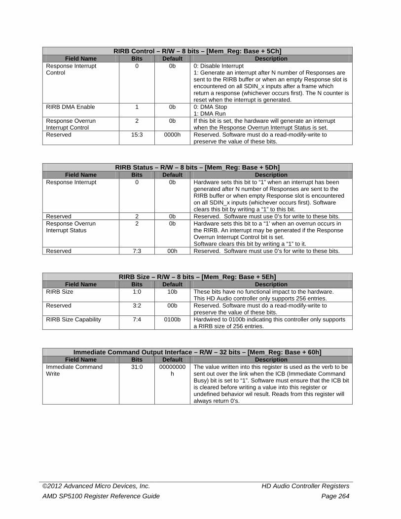
©2012 Advanced Micro Devices, Inc. HD Audio Controller Registers AMD SP5100 Register Reference Guide Page 264
RIRB Control – R/W – 8 bits – [Mem_Reg: Base + 5Ch] Field Name Bits Default Description
Response Interrupt Control
0 0b 0: Disable Interrupt 1: Generate an interrupt after N number of Responses are sent to the RIRB buffer or when an empty Response slot is encountered on all SDIN_x inputs after a frame which return a response (whichever occurs first). The N counter is reset when the interrupt is generated.
RIRB DMA Enable 1 0b 0: DMA Stop 1: DMA Run
Response Overrun Interrupt Control
2 0b If this bit is set, the hardware will generate an interrupt when the Response Overrun Interrupt Status is set.
Reserved 15:3 0000h Reserved. Software must do a read-modify-write to preserve the value of these bits.
RIRB Status – R/W – 8 bits – [Mem_Reg: Base + 5Dh] Field Name Bits Default Description
Response Interrupt 0 0b Hardware sets this bit to “1” when an interrupt has been generated after N number of Responses are sent to the RIRB buffer or when empty Response slot is encountered on all SDIN_x inputs (whichever occurs first). Software clears this bit by writing a “1” to this bit.
Reserved 2 0b Reserved. Software must use 0’s for write to these bits. Response Overrun Interrupt Status
2 0b Hardware sets this bit to a “1’ when an overrun occurs in the RIRB. An interrupt may be generated if the Response Overrun Interrupt Control bit is set. Software clears this bit by writing a “1” to it.
Reserved 7:3 00h Reserved. Software must use 0’s for write to these bits.
RIRB Size – R/W – 8 bits – [Mem_Reg: Base + 5Eh] Field Name Bits Default Description
RIRB Size 1:0 10b These bits have no functional impact to the hardware. This HD Audio controller only supports 256 entries.
Reserved 3:2 00b Reserved. Software must do a read-modify-write to preserve the value of these bits.
RIRB Size Capability 7:4 0100b Hardwired to 0100b indicating this controller only supports a RIRB size of 256 entries.
Immediate Command Output Interface – R/W – 32 bits – [Mem_Reg: Base + 60h] Field Name Bits Default Description
Immediate Command Write
31:0 00000000h
The value written into this register is used as the verb to be sent out over the link when the ICB (Immediate Command Busy) bit is set to “1”. Software must ensure that the ICB bit is cleared before writing a value into this register or undefined behavior wil result. Reads from this register will always return 0’s.
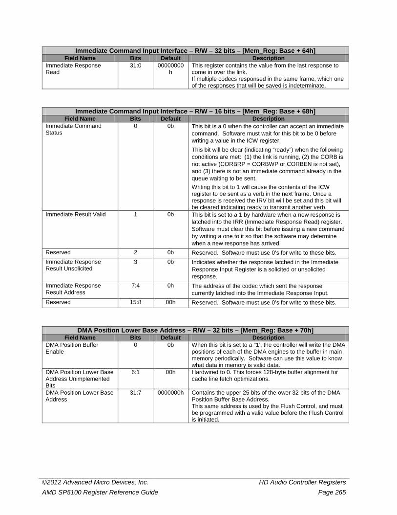
©2012 Advanced Micro Devices, Inc. HD Audio Controller Registers AMD SP5100 Register Reference Guide Page 265
Immediate Command Input Interface – R/W – 32 bits – [Mem_Reg: Base + 64h] Field Name Bits Default Description
Immediate Response Read
31:0 00000000h
This register contains the value from the last response to come in over the link. If multiple codecs responsed in the same frame, which one of the responses that will be saved is indeterminate.
Immediate Command Input Interface – R/W – 16 bits – [Mem_Reg: Base + 68h] Field Name Bits Default Description
Immediate Command Status
0 0b This bit is a 0 when the controller can accept an immediate command. Software must wait for this bit to be 0 before writing a value in the ICW register. This bit will be clear (indicating “ready”) when the following conditions are met: (1) the link is running, (2) the CORB is not active (CORBRP = CORBWP or CORBEN is not set), and (3) there is not an immediate command already in the queue waiting to be sent. Writing this bit to 1 will cause the contents of the ICW register to be sent as a verb in the next frame. Once a response is received the IRV bit will be set and this bit will be cleared indicating ready to transmit another verb.
Immediate Result Valid 1 0b This bit is set to a 1 by hardware when a new response is latched into the IRR (Immediate Response Read) register. Software must clear this bit before issuing a new command by writing a one to it so that the software may determine when a new response has arrived.
Reserved 2 0b Reserved. Software must use 0’s for write to these bits. Immediate Response Result Unsolicited
3 0b Indicates whether the response latched in the Immediate Response Input Register is a solicited or unsolicited response.
Immediate Response Result Address
7:4 0h The address of the codec which sent the response currently latched into the Immediate Response Input.
Reserved 15:8 00h Reserved. Software must use 0’s for write to these bits.
DMA Position Lower Base Address – R/W – 32 bits – [Mem_Reg: Base + 70h] Field Name Bits Default Description
DMA Position Buffer Enable
0 0b When this bit is set to a “1’, the controller will write the DMA positions of each of the DMA engines to the buffer in main memory periodically. Software can use this value to know what data in memory is valid data.
DMA Position Lower Base Address Unimplemented Bits
6:1 00h Hardwired to 0. This forces 128-byte buffer alignment for cache line fetch optimizations.
DMA Position Lower Base Address
31:7 0000000h Contains the upper 25 bits of the ower 32 bits of the DMA Position Buffer Base Address. This same address is used by the Flush Control, and must be programmed with a valid value before the Flush Control is initiated.

©2012 Advanced Micro Devices, Inc. HD Audio Controller Registers AMD SP5100 Register Reference Guide Page 266
DMA Position Upper Base Address – R/W – 32 bits – [Mem_Reg: Base + 74h] Field Name Bits Default Description
DMA Position Upper Base Address
31:0 00000000h
Upper 32 bits of the DMA Position Buffer Base Address. This same address is used by the Flush Control, and must be programmed with a valid value before the Flush Control is initiated.
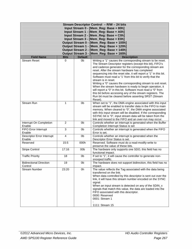
©2012 Advanced Micro Devices, Inc. HD Audio Controller Registers AMD SP5100 Register Reference Guide Page 267
Stream Descriptor Control – R/W – 24 bits Input Stream 0 - [Mem_Reg: Base + 80h] Input Stream 1 - [Mem_Reg: Base + A0h] Input Stream 2 - [Mem_Reg: Base + C0h] Input Stream 3 - [Mem_Reg: Base + E0h]
Output Stream 0 - [Mem_Reg: Base + 100h] Output Stream 1 - [Mem_Reg: Base + 120h] Output Stream 2 - [Mem_Reg: Base + 140h] Output Stream 3 - [Mem_Reg: Base + 160h]
Field Name Bits Default Description Stream Reset 0 0b Writing a “1” causes the corresponding stream to be reset.
The Stream Descriptor registers (except this bit), FIFO’s and cadence generator for the corresponding stream are reset. After the stream hardware has completed sequencing into the reset stte, it will report a “1” in this bit. Software must read a “1’ from this bit to verify that the stream is in reset. Writing a “0” causes the corresponding stream to exit reset. When the stream hardware is ready to begin operation, it will report a “0” in this bit. Software must read a “0” from this bit before accessing any of the stream registers. The Run bit must be cleared before asserting SRST (Stream Reset).
Stream Run 1 0b When set to “1”, the DMA engine associated with this input stream will be enabled to transfer data in the FIFO to main memory. When cleared to “0”, the DMA engine associated with this input stream will be disabled. If the corresponding SSYNC bit is “0”, input stream data will be taken from the link and moved to the FIFO and an over-run may occur.
Interrupt On Completion Enable
2 0b Controls whether an interrupt is generated when the Buffer Completion Interrupt Status is set
FIFO Error Interrupt Enable
3 0b Controls whether an interrupt is generated when the FIFO Error is set.
Descriptor Error Interrupt Enable
4 0b Controls whether an interrupt is generated when the Descriptor Error Status is set.
Reserved 15:5 000h Reserved. Software must do a read-modify-write to preserve the value of these bits.
Stripe Control 17:16 00b The hardware only supports one SDO, this field has no functional impact.
Traffic Priority 18 0b If set to “1”, it will cause the controller to generate non-snooped traffic.
Bidirectional Direction Control
19 0b The hardware does not support bidirection, this field has no impact.
Stream Number 23:20 0h The value reflects the Tag associated with the data being transferred on the link. When data controlled by this descriptor is sent out over the link, it will have this stream number encoded on the SYNC signal. When an input stream is detected on any of the SDIN_x signals that match this value, the data are loaded into the FIFO associated with this descriptor. 0000: Reserved 0001: Stream 1 : 1111: Stream 15
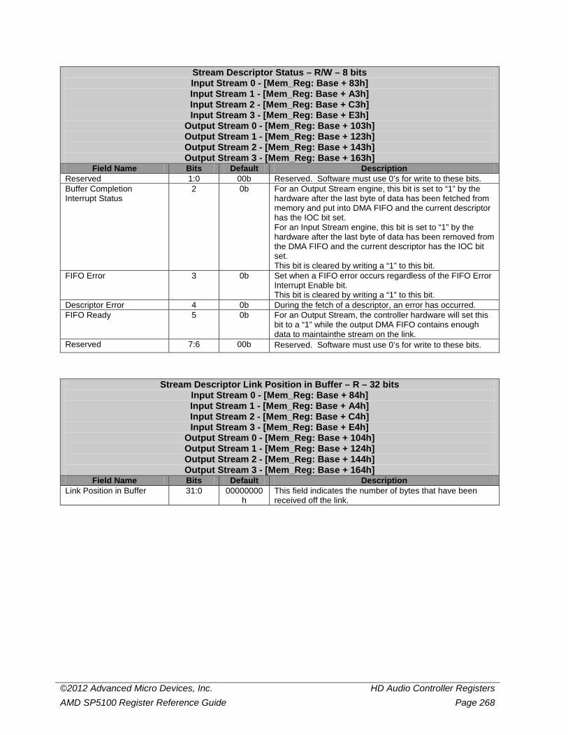
©2012 Advanced Micro Devices, Inc. HD Audio Controller Registers AMD SP5100 Register Reference Guide Page 268
Stream Descriptor Status – R/W – 8 bits Input Stream 0 - [Mem_Reg: Base + 83h] Input Stream 1 - [Mem_Reg: Base + A3h] Input Stream 2 - [Mem_Reg: Base + C3h] Input Stream 3 - [Mem_Reg: Base + E3h]
Output Stream 0 - [Mem_Reg: Base + 103h] Output Stream 1 - [Mem_Reg: Base + 123h] Output Stream 2 - [Mem_Reg: Base + 143h] Output Stream 3 - [Mem_Reg: Base + 163h]
Field Name Bits Default Description Reserved 1:0 00b Reserved. Software must use 0’s for write to these bits. Buffer Completion Interrupt Status
2 0b For an Output Stream engine, this bit is set to “1” by the hardware after the last byte of data has been fetched from memory and put into DMA FIFO and the current descriptor has the IOC bit set. For an Input Stream engine, this bit is set to “1” by the hardware after the last byte of data has been removed from the DMA FIFO and the current descriptor has the IOC bit set. This bit is cleared by writing a “1” to this bit.
FIFO Error 3 0b Set when a FIFO error occurs regardless of the FIFO Error Interrupt Enable bit. This bit is cleared by writing a “1” to this bit.
Descriptor Error 4 0b During the fetch of a descriptor, an error has occurred. FIFO Ready 5 0b For an Output Stream, the controller hardware will set this
bit to a “1” while the output DMA FIFO contains enough data to maintainthe stream on the link.
Reserved 7:6 00b Reserved. Software must use 0’s for write to these bits.
Stream Descriptor Link Position in Buffer – R – 32 bits Input Stream 0 - [Mem_Reg: Base + 84h] Input Stream 1 - [Mem_Reg: Base + A4h] Input Stream 2 - [Mem_Reg: Base + C4h] Input Stream 3 - [Mem_Reg: Base + E4h]
Output Stream 0 - [Mem_Reg: Base + 104h] Output Stream 1 - [Mem_Reg: Base + 124h] Output Stream 2 - [Mem_Reg: Base + 144h] Output Stream 3 - [Mem_Reg: Base + 164h]
Field Name Bits Default Description Link Position in Buffer 31:0 00000000
h This field indicates the number of bytes that have been received off the link.
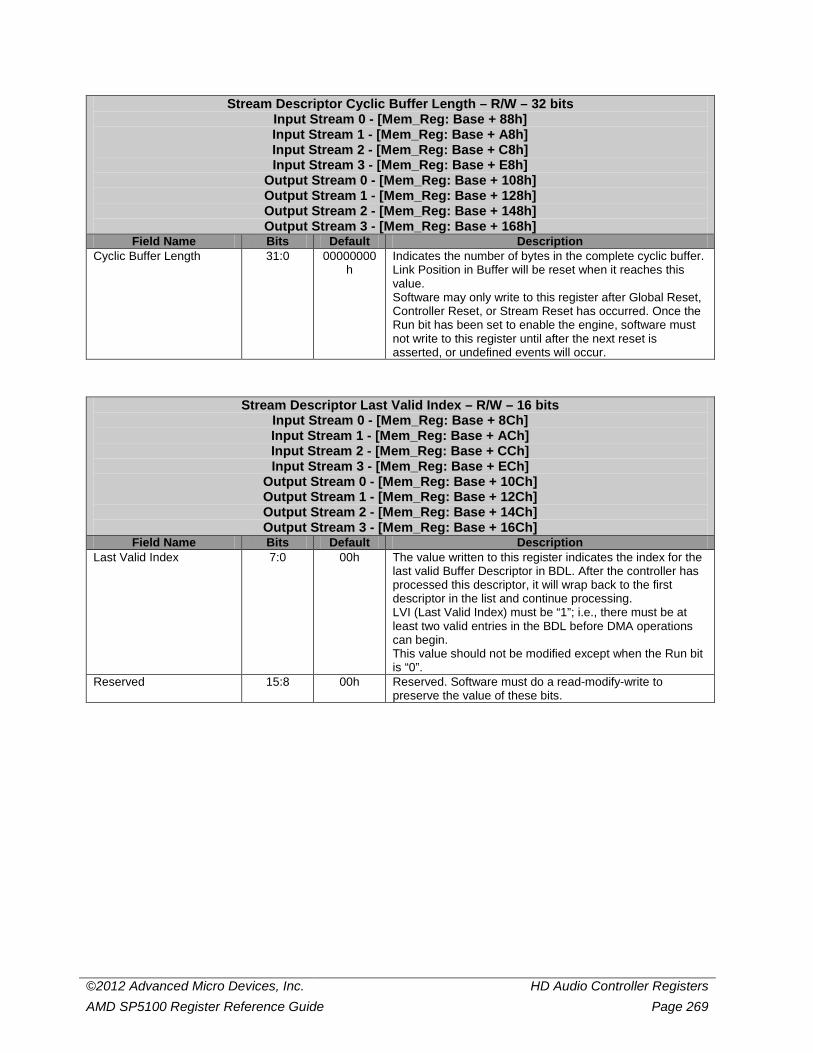
©2012 Advanced Micro Devices, Inc. HD Audio Controller Registers AMD SP5100 Register Reference Guide Page 269
Stream Descriptor Cyclic Buffer Length – R/W – 32 bits Input Stream 0 - [Mem_Reg: Base + 88h] Input Stream 1 - [Mem_Reg: Base + A8h] Input Stream 2 - [Mem_Reg: Base + C8h] Input Stream 3 - [Mem_Reg: Base + E8h]
Output Stream 0 - [Mem_Reg: Base + 108h] Output Stream 1 - [Mem_Reg: Base + 128h] Output Stream 2 - [Mem_Reg: Base + 148h] Output Stream 3 - [Mem_Reg: Base + 168h]
Field Name Bits Default Description Cyclic Buffer Length 31:0 00000000
h Indicates the number of bytes in the complete cyclic buffer. Link Position in Buffer will be reset when it reaches this value. Software may only write to this register after Global Reset, Controller Reset, or Stream Reset has occurred. Once the Run bit has been set to enable the engine, software must not write to this register until after the next reset is asserted, or undefined events will occur.
Stream Descriptor Last Valid Index – R/W – 16 bits Input Stream 0 - [Mem_Reg: Base + 8Ch] Input Stream 1 - [Mem_Reg: Base + ACh] Input Stream 2 - [Mem_Reg: Base + CCh] Input Stream 3 - [Mem_Reg: Base + ECh]
Output Stream 0 - [Mem_Reg: Base + 10Ch] Output Stream 1 - [Mem_Reg: Base + 12Ch] Output Stream 2 - [Mem_Reg: Base + 14Ch] Output Stream 3 - [Mem_Reg: Base + 16Ch]
Field Name Bits Default Description Last Valid Index 7:0 00h The value written to this register indicates the index for the
last valid Buffer Descriptor in BDL. After the controller has processed this descriptor, it will wrap back to the first descriptor in the list and continue processing. LVI (Last Valid Index) must be “1”; i.e., there must be at least two valid entries in the BDL before DMA operations can begin. This value should not be modified except when the Run bit is “0”.
Reserved 15:8 00h Reserved. Software must do a read-modify-write to preserve the value of these bits.
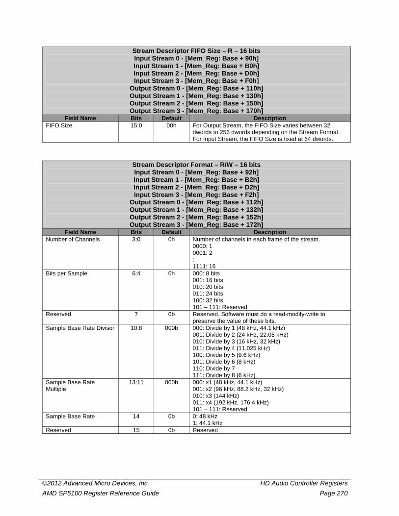
©2012 Advanced Micro Devices, Inc. HD Audio Controller Registers AMD SP5100 Register Reference Guide Page 270
Stream Descriptor FIFO Size – R – 16 bits Input Stream 0 - [Mem_Reg: Base + 90h] Input Stream 1 - [Mem_Reg: Base + B0h] Input Stream 2 - [Mem_Reg: Base + D0h] Input Stream 3 - [Mem_Reg: Base + F0h]
Output Stream 0 - [Mem_Reg: Base + 110h] Output Stream 1 - [Mem_Reg: Base + 130h] Output Stream 2 - [Mem_Reg: Base + 150h] Output Stream 3 - [Mem_Reg: Base + 170h]
Field Name Bits Default Description FIFO Size 15:0 00h For Output Stream, the FIFO Size varies between 32
dwords to 256 dwords depending on the Stream Format. For Input Stream, the FIFO Size is fixed at 64 dwords.
Stream Descriptor Format – R/W – 16 bits Input Stream 0 - [Mem_Reg: Base + 92h] Input Stream 1 - [Mem_Reg: Base + B2h] Input Stream 2 - [Mem_Reg: Base + D2h] Input Stream 3 - [Mem_Reg: Base + F2h]
Output Stream 0 - [Mem_Reg: Base + 112h] Output Stream 1 - [Mem_Reg: Base + 132h] Output Stream 2 - [Mem_Reg: Base + 152h] Output Stream 3 - [Mem_Reg: Base + 172h]
Field Name Bits Default Description Number of Channels 3:0 0h Number of channels in each frame of the stream.
0000: 1 0001: 2 : 1111: 16
Bits per Sample 6:4 0h 000: 8 bits 001: 16 bits 010: 20 bits 011: 24 bits 100: 32 bits 101 – 111: Reserved
Reserved 7 0b Reserved. Software must do a read-modify-write to preserve the value of these bits.
Sample Base Rate Divisor 10:8 000b 000: Divide by 1 (48 kHz, 44.1 kHz) 001: Divide by 2 (24 kHz, 22.05 kHz) 010: Divide by 3 (16 kHz, 32 kHz) 011: Divide by 4 (11.025 kHz) 100: Divide by 5 (9.6 kHz) 101: Divide by 6 (8 kHz) 110: Divide by 7 111: Divide by 8 (6 kHz)
Sample Base Rate Multiple
13:11 000b 000: x1 (48 kHz, 44.1 kHz) 001: x2 (96 kHz, 88.2 kHz, 32 kHz) 010: x3 (144 kHz) 011: x4 (192 kHz, 176.4 kHz) 101 – 111: Reserved
Sample Base Rate 14 0b 0: 48 kHz 1: 44.1 kHz
Reserved 15 0b Reserved

©2012 Advanced Micro Devices, Inc. HD Audio Controller Registers AMD SP5100 Register Reference Guide Page 271
Stream Descriptor BDL Pointer Lower Base Address – R/W – 32 bits Input Stream 0 - [Mem_Reg: Base + 98h] Input Stream 1 - [Mem_Reg: Base + B8h] Input Stream 2 - [Mem_Reg: Base + D8h] Input Stream 3 - [Mem_Reg: Base + F8h]
Output Stream 0 - [Mem_Reg: Base + 138h] Output Stream 2 - [Mem_Reg: Base + 158h] Output Stream 3 - [Mem_Reg: Base + 178h]
Field Name Bits Default Description Reserved 6:0 00h Hardwired to 0’s to force 128 byte alignment of the BDL. Buffer Descriptor List Lower Base Address
31:7 0000000h Upper 25 bits of the lower 32 bit address of the Buffer Descriptor List. This value should not be modified except when the Run bit is “0”.
Stream Descriptor BDL Pointer Upper Base Address – R/W – 32 bits Input Stream 0 - [Mem_Reg: Base + 9Ch] Input Stream 1 - [Mem_Reg: Base + BCh] Input Stream 2 - [Mem_Reg: Base + DCh] Input Stream 3 - [Mem_Reg: Base + FCh]
Output Stream 0 - [Mem_Reg: Base + 11Ch] Output Stream 1 - [Mem_Reg: Base + 13Ch] Output Stream 2 - [Mem_Reg: Base + 15Ch] Output Stream 3 - [Mem_Reg: Base + 17Ch]
Field Name Bits Default Description Buffer Descriptor List Upper Base Address
31:0 00000000h
Upper 32 bit address of the Buffer Descriptor List. This value should not be modified except when the Run bit is “0”.
Wall Clock Counter Alias – R – 32 bits – [Mem_Reg: Base + 2030h] Field Name Bits Default Description
Wall Clock Counter Alias 31:0 00000000h
An alias of the Wall Clock Counter register at offset 0x30. It behaves exactly the same as if the Wall Clock Counter register were being read directly.
Stream Descriptor Link Position in Buffer Alias – R – 32 bits Input Stream 0 - [Mem_Reg: Base + 2084h] Input Stream 1 - [Mem_Reg: Base + 20A4h] Input Stream 2 - [Mem_Reg: Base + 20C4h] Input Stream 3 - [Mem_Reg: Base + 20E4h]
Output Stream 0 - [Mem_Reg: Base + 2104h] Output Stream 1 - [Mem_Reg: Base + 2124h] Output Stream 2 - [Mem_Reg: Base + 2144h] Output Stream 3 - [Mem_Reg: Base + 2164h]
Field Name Bits Default Description Link Position in Buffer Alias
31:0 00000000h
An alias of the Link Position in Buffer register of each Stream Descriptor.
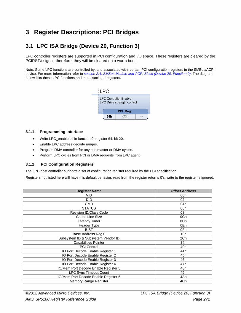
©2012 Advanced Micro Devices, Inc. LPC ISA Bridge (Device 20, Function 3) AMD SP5100 Register Reference Guide Page 272
3 Register Descriptions: PCI Bridges
3.1 LPC ISA Bridge (Device 20, Function 3)
LPC controller registers are supported in PCI configuration and I/O space. These registers are cleared by the PCIRST# signal; therefore, they will be cleared on a warm boot. Note: Some LPC functions are controlled by, and associated with, certain PCI configuration registers in the SMBus/ACPI device. For more information refer to section 2.4: SMBus Module and ACPI Block (Device 20, Function 0). The diagram below lists these LPC functions and the associated registers.
3.1.1 Programming Interface
• Write LPC_enable bit in function 0, register 64, bit 20. • Enable LPC address decode ranges. • Program DMA controller for any bus master or DMA cycles. • Perform LPC cycles from PCI or DMA requests from LPC agent.
3.1.2 PCI Configuration Registers The LPC host controller supports a set of configuration register required by the PCI specification.
Registers not listed here will have this default behavior: read from the register returns 0’s; write to the register is ignored.
Register Name Offset Address VID 00h DID 02h
CMD 04h STATUS 06h
Revision ID/Class Code 08h Cache Line Size 0Ch Latency Timer 0Dh Header Type 0Eh
BIST 0Fh Base Address Reg 0 10h
Subsystem ID & Subsystem Vendor ID 2Ch Capabilities Pointer 34h
PCI Control 40h IO Port Decode Enable Register 1 44h IO Port Decode Enable Register 2 45h IO Port Decode Enable Register 3 46h IO Port Decode Enable Register 4 47h
IO/Mem Port Decode Enable Register 5 48h LPC Sync Timeout Count 49h
IO/Mem Port Decode Enable Register 6 4Ah Memory Range Register 4Ch

©2012 Advanced Micro Devices, Inc. LPC ISA Bridge (Device 20, Function 3) AMD SP5100 Register Reference Guide Page 273
Register Name Offset Address Rom Protect 0 50h Rom Protect 1 54h Rom Protect 2 58h Rom Protect 3 5Ch
PCI Memory Start Address for LPC Target Cycles 60h PCI Memory End Address for LPC Target Cycles 62h
PCI IO base Address for Wide Generic Port 64h LPC ROM Address Range 1 (Start Address) 68h LPC ROM Address Range 1 (End Address) 6Ah LPC ROM Address Range 2 (Start Address) 6Ch LPC ROM Address Range 2 (End Address) 6Eh
Firmware Hub Select 70h Alternative Wide Io Range Enable 74h
Reserved 78h TPM register 7Ch
LPCCLKCntl register 7Dh MSI Capability register 80h TMKBC_BaseAddrLow 84h TMKBC_BaseAddrHigh 88h
TMKBC_Remap 8Ch Wide_IO2 90h
ImcGpioCntrl 92h IMCaCntrl 94h IMCbCntrl 96h
HostOwnLPC 98h ImcOwnLPC 99h
reserved 9Ch SPI Base_Addr A0h
IMC_PortAddress A4h RomDmaSrcAddr B0h
RomDmaTargetAddr B4h RomDmaControl B8h
ImcControl BAh HostControl BBh
ImcInstrRomPage BCh ImcInstrMemPage BEh ImcRomFlashPage C0h ImcLpcMemPage C2h
ImcDataPage C4h ImcGpio_Out C6h ImcGpio_OeB C8h ImcGpioStatus CAh
ImcGpio_PDControl CCh ImcGpio_PUControl CEh
IMCa_Out D0h IMCa_OeB D1h
IMCa_Status D2h IMCa_PDControl D3h IMCa_PUControl D4h
IMCb_Out D5h IMCb_OeB D7h
IMCb_Status D9h IMCb_PDControl DBh IMCb_PUControl DDh
IMC_Misc1 DFh
Note: PCI function 3 configuration registers are described below.
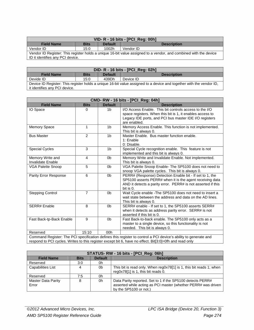
©2012 Advanced Micro Devices, Inc. LPC ISA Bridge (Device 20, Function 3) AMD SP5100 Register Reference Guide Page 274
VID- R - 16 bits - [PCI_Reg: 00h] Field Name Bits Default Description
Vendor ID 15:0 1002h Vendor ID Vendor ID Register: This register holds a unique 16-bit value assigned to a vendor, and combined with the device ID it identifies any PCI device.
DID- R - 16 bits - [PCI_Reg: 02h] Field Name Bits Default Description
Devide ID 15:0 439Dh Device ID Device ID Register: This register holds a unique 16-bit value assigned to a device and together with the vendor ID, it identifies any PCI device.
CMD- RW - 16 bits - [PCI_Reg: 04h] Field Name Bits Default Description
IO Space 0 1b I/O Access Enable. This bit controls access to the I/O space registers. When this bit is 1, it enables access to Legacy IDE ports, and PCI bus master IDE I/O registers are enabled.
Memory Space 1 1b Memory Access Enable. This function is not implemented. This bit is always 0.
Bus Master 2 1b Master Enable. Bus master function enable. 1: Enable 0: Disable.
Special Cycles 3 1b Special Cycle recognition enable. This feature is not implemented and this bit is always 0.
Memory Write and Invalidate Enable
4 0b Memory Write and Invalidate Enable. Not implemented. This bit is always 0.
VGA Palette Snoop 5 0b VGA Palette Snoop Enable- The SP5100 does not need to snoop VGA palette cycles. This bit is always 0.
Parity Error Response 6 0b PERR# (Response) Detection Enable bit - If set to 1, the SP5100 asserts PERR# when it is the agent receiving data AND it detects a parity error. PERR# is not asserted if this bit is 0.
Stepping Control 7 0b Wait Cycle enable -The SP5100 does not need to insert a wait state between the address and data on the AD lines. This bit is always 0.
SERR# Enable 8 0b SERR# enable - If set to 1, the SP5100 asserts SERR# when it detects as address parity error. SERR# is not asserted if this bit is 0.
Fast Back-tp-Back Enable 9 0b Fast Back-to-back enable. The SP5100 only acts as a master to a single device, so this functionality is not needed. This bit is always 0.
Reserved 15:10 00h Command Register: The PCI specification defines this register to control a PCI device’s ability to generate and respond to PCI cycles. Writes to this register except bit 6, have no effect. Bit[3:0]=0fh and read only
STATUS- RW - 16 bits - [PCI_Reg: 06h] Field Name Bits Default Description
Reserved 3:0 0h Capabilities List 4 0b This bit is read only. When reg0x78[1] is 1, this bit reads 1; when
reg0x78[1] is 1, this bit reads 0. Reserved 7:5 0h Master Data Parity Error
8 0h Data Parity reported. Set to 1 if the SP5100 detects PERR# asserted while acting as PCI master (whether PERR# was driven by the SP5100 or not.)
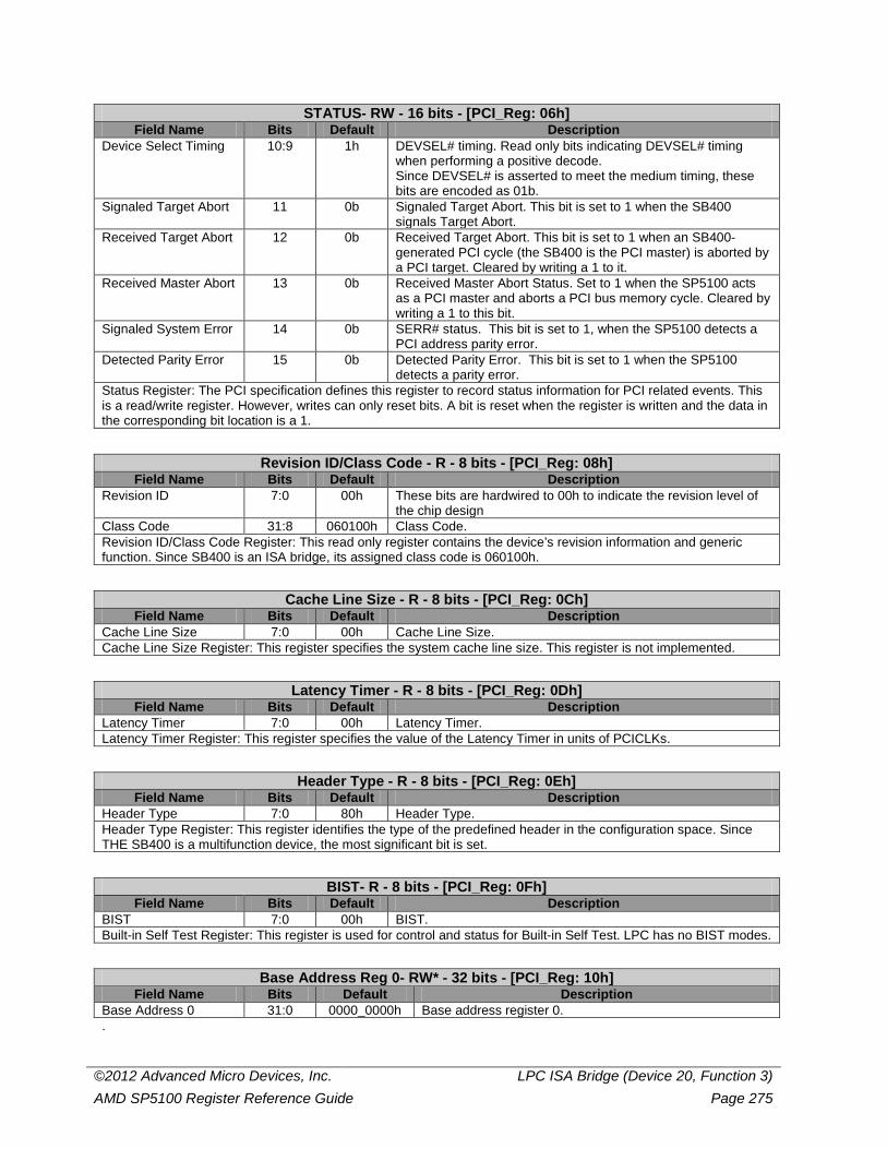
©2012 Advanced Micro Devices, Inc. LPC ISA Bridge (Device 20, Function 3) AMD SP5100 Register Reference Guide Page 275
STATUS- RW - 16 bits - [PCI_Reg: 06h] Field Name Bits Default Description
Device Select Timing 10:9 1h DEVSEL# timing. Read only bits indicating DEVSEL# timing when performing a positive decode. Since DEVSEL# is asserted to meet the medium timing, these bits are encoded as 01b.
Signaled Target Abort 11 0b Signaled Target Abort. This bit is set to 1 when the SB400 signals Target Abort.
Received Target Abort 12 0b Received Target Abort. This bit is set to 1 when an SB400-generated PCI cycle (the SB400 is the PCI master) is aborted by a PCI target. Cleared by writing a 1 to it.
Received Master Abort 13 0b Received Master Abort Status. Set to 1 when the SP5100 acts as a PCI master and aborts a PCI bus memory cycle. Cleared by writing a 1 to this bit.
Signaled System Error 14 0b SERR# status. This bit is set to 1, when the SP5100 detects a PCI address parity error.
Detected Parity Error 15 0b Detected Parity Error. This bit is set to 1 when the SP5100 detects a parity error.
Status Register: The PCI specification defines this register to record status information for PCI related events. This is a read/write register. However, writes can only reset bits. A bit is reset when the register is written and the data in the corresponding bit location is a 1.
Revision ID/Class Code - R - 8 bits - [PCI_Reg: 08h] Field Name Bits Default Description
Revision ID
7:0 00h These bits are hardwired to 00h to indicate the revision level of the chip design
Class Code 31:8 060100h Class Code. Revision ID/Class Code Register: This read only register contains the device’s revision information and generic function. Since SB400 is an ISA bridge, its assigned class code is 060100h.
Cache Line Size - R - 8 bits - [PCI_Reg: 0Ch] Field Name Bits Default Description
Cache Line Size 7:0 00h Cache Line Size. Cache Line Size Register: This register specifies the system cache line size. This register is not implemented.
Latency Timer - R - 8 bits - [PCI_Reg: 0Dh] Field Name Bits Default Description
Latency Timer 7:0 00h Latency Timer. Latency Timer Register: This register specifies the value of the Latency Timer in units of PCICLKs.
Header Type - R - 8 bits - [PCI_Reg: 0Eh] Field Name Bits Default Description
Header Type 7:0 80h Header Type. Header Type Register: This register identifies the type of the predefined header in the configuration space. Since THE SB400 is a multifunction device, the most significant bit is set.
BIST- R - 8 bits - [PCI_Reg: 0Fh] Field Name Bits Default Description
BIST 7:0 00h BIST. Built-in Self Test Register: This register is used for control and status for Built-in Self Test. LPC has no BIST modes.
Base Address Reg 0- RW* - 32 bits - [PCI_Reg: 10h] Field Name Bits Default Description
Base Address 0 31:0 0000_0000h Base address register 0. .
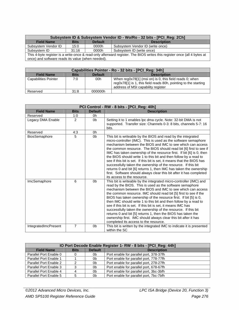
©2012 Advanced Micro Devices, Inc. LPC ISA Bridge (Device 20, Function 3) AMD SP5100 Register Reference Guide Page 276
Subsystem ID & Subsystem Vendor ID - Wo/Ro - 32 bits - [PCI_Reg: 2Ch] Field Name Bits Default Description
Subsystem Vendor ID 15:0 0000h Subsystem Vendor ID (write once) Subsystem ID 31:16 0000h Subsystem ID (write once) This 4-byte register is a write-once & read-only afterward register. The BIOS writes this register once (all 4 bytes at once) and software reads its value (when needed).
Capabilities Pointer - Ro - 32 bits - [PCI_Reg: 34h] Field Name Bits Default Description
Capabilities Pointer 7:0 00h When reg0x78[1] (msi on) is 0, this field reads 0; when reg0x78[1] is 1, this field reads 80h, pointing to the starting address of MSI capability register
Reserved 31:8 000000h
PCI Control - RW - 8 bits - [PCI_Reg: 40h] Field Name Bits Default Description
Reserved 1:0 0h Legacy DMA Enable 2 0b Setting it to 1 enables lpc dma cycle. Note: 32-bit DMA is not
supported. Transfer size: Channels 0-3: 8 bits, channels 5-7: 16 bits.
Reserved 4:3 0h BiosSemaphore 5 0b This bit is writeable by the BIOS and read by the integrated
micro-controller (IMC). This is used as the software semaphore mechanism between the BIOS and IMC to see which can access the common resource. The BIOS should read bit [6] first to see if IMC has taken ownership of the resource first. If bit [6] is 0, then the BIOS should write 1 to this bit and then follow by a read to see if this bit is set. If this bit is set, it means that the BIOS has successfully taken the ownership of the resource. If this bit returns 0 and bit [6] returns 1, then IMC has taken the ownership first. Software should always clear this bit after it has completed its access to the resource.
ImcSemaphore 6 0b This bit is writeable by the integrated micro-controller (IMC) and read by the BIOS. This is used as the software semaphore mechanism between the BIOS and IMC to see which can access the common resource. IMC should read bit [5] first to see if the BIOS has taken ownership of the resource first. If bit [5] is 0, then IMC should write 1 to this bit and then follow by a read to see if this bit is set. If this bit is set, it means IMC has successfully taken the ownership of the resource. If this bit returns 0 and bit [5] returns 1, then the BIOS has taken the ownership first. IMC should always clear this bit after it has completed its access to the resource.
IntegratedImcPresent 7 0b This bit is written by the integrated IMC to indicate it is presented within the SC
IO Port Decode Enable Register 1- RW - 8 bits - [PCI_Reg: 44h] Field Name Bits Default Description
Parallel Port Enable 0 0 0b Port enable for parallel port, 378-37fh Parallel Port Enable 1 1 0b Port enable for parallel port, 778-77fh Parallel Port Enable 2 2 0b Port enable for parallel port, 278-27fh Parallel Port Enable 3 3 0b Port enable for parallel port, 678-67fh Parallel Port Enable 4 4 0b Port enable for parallel port, 3bc-3bfh Parallel Port Enable 5 5 0b Port enable for parallel port, 7bc-7bfh
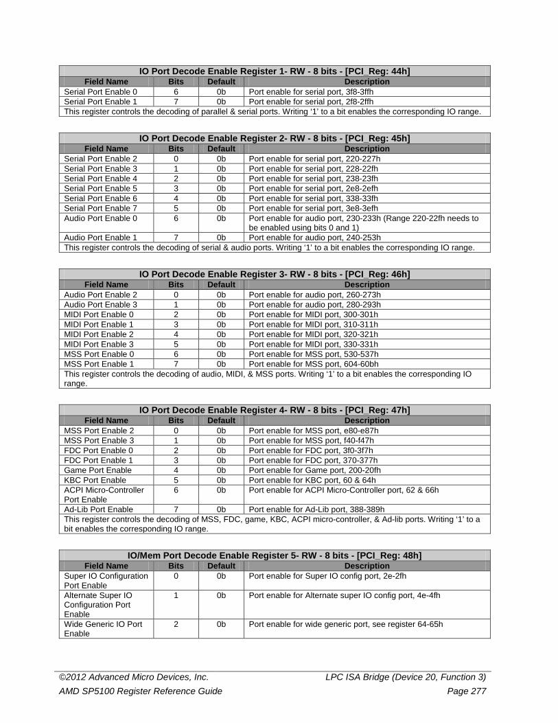
©2012 Advanced Micro Devices, Inc. LPC ISA Bridge (Device 20, Function 3) AMD SP5100 Register Reference Guide Page 277
IO Port Decode Enable Register 1- RW - 8 bits - [PCI_Reg: 44h] Field Name Bits Default Description
Serial Port Enable 0 6 0b Port enable for serial port, 3f8-3ffh Serial Port Enable 1 7 0b Port enable for serial port, 2f8-2ffh This register controls the decoding of parallel & serial ports. Writing ‘1’ to a bit enables the corresponding IO range.
IO Port Decode Enable Register 2- RW - 8 bits - [PCI_Reg: 45h] Field Name Bits Default Description
Serial Port Enable 2 0 0b Port enable for serial port, 220-227h Serial Port Enable 3 1 0b Port enable for serial port, 228-22fh Serial Port Enable 4 2 0b Port enable for serial port, 238-23fh Serial Port Enable 5 3 0b Port enable for serial port, 2e8-2efh Serial Port Enable 6 4 0b Port enable for serial port, 338-33fh Serial Port Enable 7 5 0b Port enable for serial port, 3e8-3efh Audio Port Enable 0 6 0b Port enable for audio port, 230-233h (Range 220-22fh needs to
be enabled using bits 0 and 1) Audio Port Enable 1 7 0b Port enable for audio port, 240-253h This register controls the decoding of serial & audio ports. Writing ‘1’ to a bit enables the corresponding IO range.
IO Port Decode Enable Register 3- RW - 8 bits - [PCI_Reg: 46h] Field Name Bits Default Description
Audio Port Enable 2 0 0b Port enable for audio port, 260-273h Audio Port Enable 3 1 0b Port enable for audio port, 280-293h MIDI Port Enable 0 2 0b Port enable for MIDI port, 300-301h MIDI Port Enable 1 3 0b Port enable for MIDI port, 310-311h MIDI Port Enable 2 4 0b Port enable for MIDI port, 320-321h MIDI Port Enable 3 5 0b Port enable for MIDI port, 330-331h MSS Port Enable 0 6 0b Port enable for MSS port, 530-537h MSS Port Enable 1 7 0b Port enable for MSS port, 604-60bh This register controls the decoding of audio, MIDI, & MSS ports. Writing ‘1’ to a bit enables the corresponding IO range.
IO Port Decode Enable Register 4- RW - 8 bits - [PCI_Reg: 47h] Field Name Bits Default Description
MSS Port Enable 2 0 0b Port enable for MSS port, e80-e87h MSS Port Enable 3 1 0b Port enable for MSS port, f40-f47h FDC Port Enable 0 2 0b Port enable for FDC port, 3f0-3f7h FDC Port Enable 1 3 0b Port enable for FDC port, 370-377h Game Port Enable 4 0b Port enable for Game port, 200-20fh KBC Port Enable 5 0b Port enable for KBC port, 60 & 64h ACPI Micro-Controller Port Enable
6 0b Port enable for ACPI Micro-Controller port, 62 & 66h
Ad-Lib Port Enable 7 0b Port enable for Ad-Lib port, 388-389h This register controls the decoding of MSS, FDC, game, KBC, ACPI micro-controller, & Ad-lib ports. Writing ‘1’ to a bit enables the corresponding IO range.
IO/Mem Port Decode Enable Register 5- RW - 8 bits - [PCI_Reg: 48h] Field Name Bits Default Description
Super IO Configuration Port Enable
0 0b Port enable for Super IO config port, 2e-2fh
Alternate Super IO Configuration Port Enable
1 0b Port enable for Alternate super IO config port, 4e-4fh
Wide Generic IO Port Enable
2 0b Port enable for wide generic port, see register 64-65h
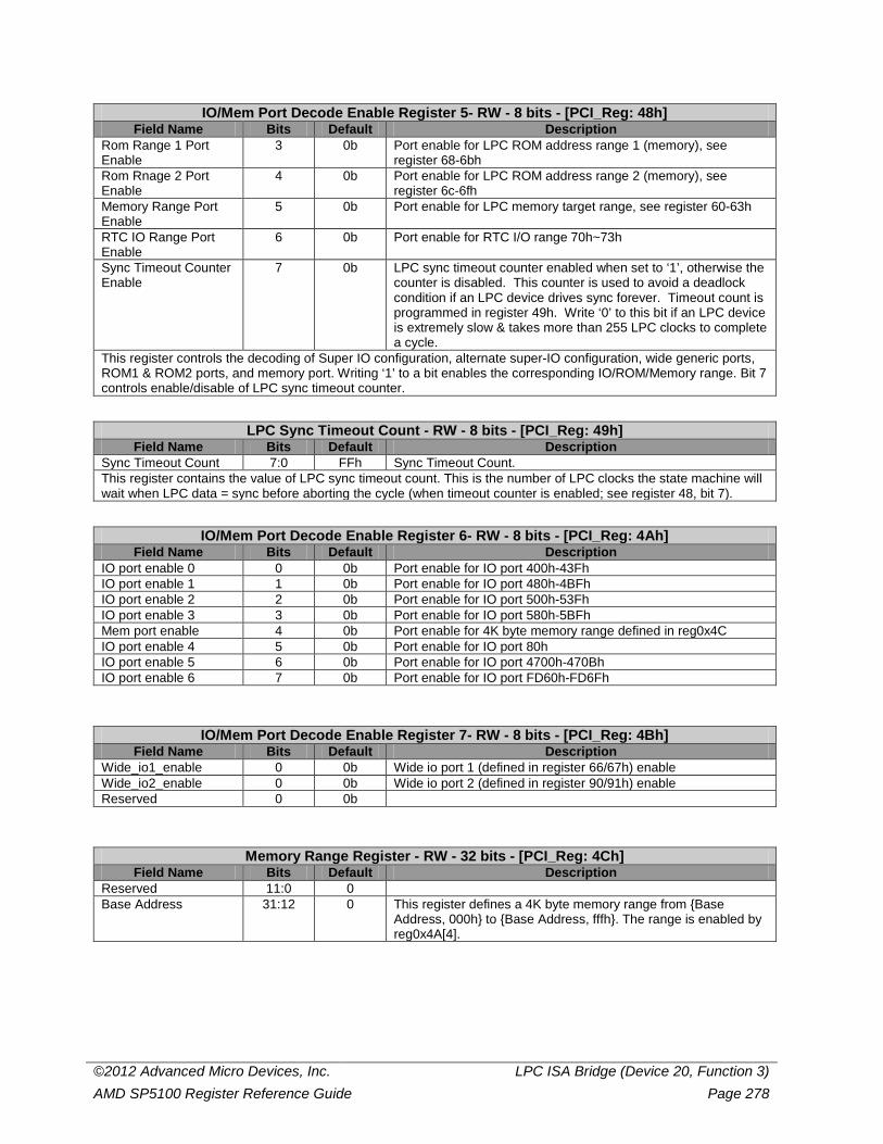
©2012 Advanced Micro Devices, Inc. LPC ISA Bridge (Device 20, Function 3) AMD SP5100 Register Reference Guide Page 278
IO/Mem Port Decode Enable Register 5- RW - 8 bits - [PCI_Reg: 48h] Field Name Bits Default Description
Rom Range 1 Port Enable
3 0b Port enable for LPC ROM address range 1 (memory), see register 68-6bh
Rom Rnage 2 Port Enable
4 0b Port enable for LPC ROM address range 2 (memory), see register 6c-6fh
Memory Range Port Enable
5 0b Port enable for LPC memory target range, see register 60-63h
RTC IO Range Port Enable
6 0b Port enable for RTC I/O range 70h~73h
Sync Timeout Counter Enable
7 0b LPC sync timeout counter enabled when set to ‘1’, otherwise the counter is disabled. This counter is used to avoid a deadlock condition if an LPC device drives sync forever. Timeout count is programmed in register 49h. Write ‘0’ to this bit if an LPC device is extremely slow & takes more than 255 LPC clocks to complete a cycle.
This register controls the decoding of Super IO configuration, alternate super-IO configuration, wide generic ports, ROM1 & ROM2 ports, and memory port. Writing ‘1’ to a bit enables the corresponding IO/ROM/Memory range. Bit 7 controls enable/disable of LPC sync timeout counter.
LPC Sync Timeout Count - RW - 8 bits - [PCI_Reg: 49h] Field Name Bits Default Description
Sync Timeout Count 7:0 FFh Sync Timeout Count. This register contains the value of LPC sync timeout count. This is the number of LPC clocks the state machine will wait when LPC data = sync before aborting the cycle (when timeout counter is enabled; see register 48, bit 7).
IO/Mem Port Decode Enable Register 6- RW - 8 bits - [PCI_Reg: 4Ah] Field Name Bits Default Description
IO port enable 0 0 0b Port enable for IO port 400h-43Fh IO port enable 1 1 0b Port enable for IO port 480h-4BFh IO port enable 2 2 0b Port enable for IO port 500h-53Fh IO port enable 3 3 0b Port enable for IO port 580h-5BFh Mem port enable 4 0b Port enable for 4K byte memory range defined in reg0x4C IO port enable 4 5 0b Port enable for IO port 80h IO port enable 5 6 0b Port enable for IO port 4700h-470Bh IO port enable 6 7 0b Port enable for IO port FD60h-FD6Fh
IO/Mem Port Decode Enable Register 7- RW - 8 bits - [PCI_Reg: 4Bh] Field Name Bits Default Description
Wide_io1_enable 0 0b Wide io port 1 (defined in register 66/67h) enable Wide_io2_enable 0 0b Wide io port 2 (defined in register 90/91h) enable Reserved 0 0b
Memory Range Register - RW - 32 bits - [PCI_Reg: 4Ch] Field Name Bits Default Description
Reserved 11:0 0 Base Address 31:12 0 This register defines a 4K byte memory range from {Base
Address, 000h} to {Base Address, fffh}. The range is enabled by reg0x4A[4].
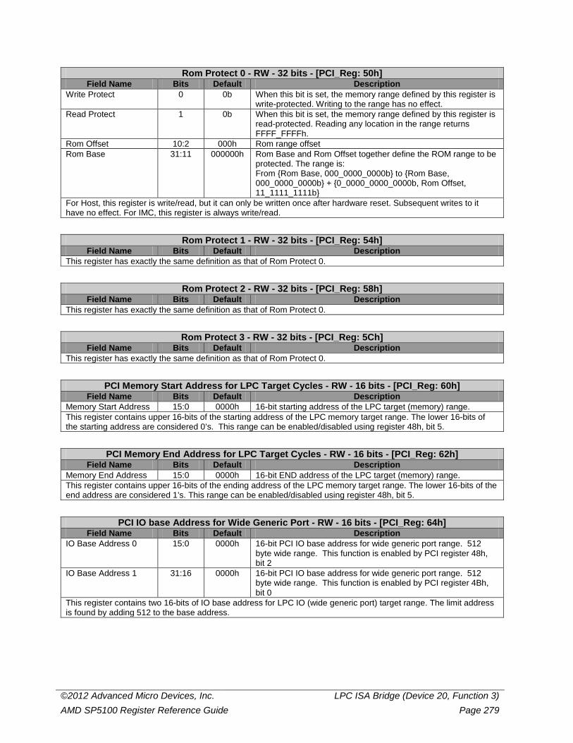
©2012 Advanced Micro Devices, Inc. LPC ISA Bridge (Device 20, Function 3) AMD SP5100 Register Reference Guide Page 279
Rom Protect 0 - RW - 32 bits - [PCI_Reg: 50h] Field Name Bits Default Description
Write Protect 0 0b When this bit is set, the memory range defined by this register is write-protected. Writing to the range has no effect.
Read Protect 1 0b When this bit is set, the memory range defined by this register is read-protected. Reading any location in the range returns FFFF_FFFFh.
Rom Offset 10:2 000h Rom range offset Rom Base 31:11 000000h Rom Base and Rom Offset together define the ROM range to be
protected. The range is: From {Rom Base, 000_0000_0000b} to {Rom Base, 000_0000_0000b} + {0_0000_0000_0000b, Rom Offset, 11_1111_1111b}
For Host, this register is write/read, but it can only be written once after hardware reset. Subsequent writes to it have no effect. For IMC, this register is always write/read.
Rom Protect 1 - RW - 32 bits - [PCI_Reg: 54h] Field Name Bits Default Description
This register has exactly the same definition as that of Rom Protect 0.
Rom Protect 2 - RW - 32 bits - [PCI_Reg: 58h] Field Name Bits Default Description
This register has exactly the same definition as that of Rom Protect 0.
Rom Protect 3 - RW - 32 bits - [PCI_Reg: 5Ch] Field Name Bits Default Description
This register has exactly the same definition as that of Rom Protect 0.
PCI Memory Start Address for LPC Target Cycles - RW - 16 bits - [PCI_Reg: 60h] Field Name Bits Default Description
Memory Start Address 15:0 0000h 16-bit starting address of the LPC target (memory) range. This register contains upper 16-bits of the starting address of the LPC memory target range. The lower 16-bits of the starting address are considered 0’s. This range can be enabled/disabled using register 48h, bit 5.
PCI Memory End Address for LPC Target Cycles - RW - 16 bits - [PCI_Reg: 62h] Field Name Bits Default Description
Memory End Address 15:0 0000h 16-bit END address of the LPC target (memory) range. This register contains upper 16-bits of the ending address of the LPC memory target range. The lower 16-bits of the end address are considered 1’s. This range can be enabled/disabled using register 48h, bit 5.
PCI IO base Address for Wide Generic Port - RW - 16 bits - [PCI_Reg: 64h] Field Name Bits Default Description
IO Base Address 0 15:0 0000h 16-bit PCI IO base address for wide generic port range. 512 byte wide range. This function is enabled by PCI register 48h, bit 2
IO Base Address 1 31:16 0000h 16-bit PCI IO base address for wide generic port range. 512 byte wide range. This function is enabled by PCI register 4Bh, bit 0
This register contains two 16-bits of IO base address for LPC IO (wide generic port) target range. The limit address is found by adding 512 to the base address.
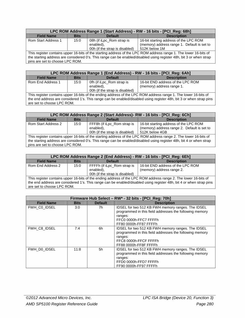
©2012 Advanced Micro Devices, Inc. LPC ISA Bridge (Device 20, Function 3) AMD SP5100 Register Reference Guide Page 280
LPC ROM Address Range 1 (Start Address) - RW - 16 bits - [PCI_Reg: 68h] Field Name Bits Default Description
Rom Start Address 1 15:0 08h (if iLpc_Rom strap is enabled), 00h (if the strap is disabled)
16-bit starting address of the LPC ROM (memory) address range 1. Default is set to 512K below 1M
This register contains upper 16-bits of the starting address of the LPC ROM address range 1. The lower 16-bits of the starting address are considered 0’s. This range can be enabled/disabled using register 48h, bit 3 or when strap pins are set to choose LPC ROM.
LPC ROM Address Range 1 (End Address) - RW - 16 bits - [PCI_Reg: 6Ah] Field Name Bits Default Description
Rom End Address 1 15:0 0fh (if iLpc_Rom strap is enabled), 00h (if the strap is disabled)
16-bit END address of the LPC ROM (memory) address range 1.
This register contains upper 16-bits of the ending address of the LPC ROM address range 1. The lower 16-bits of the end address are considered 1’s. This range can be enabled/disabled using register 48h, bit 3 or when strap pins are set to choose LPC ROM.
LPC ROM Address Range 2 (Start Address)- RW - 16 bits - [PCI_Reg: 6Ch] Field Name Bits Default Description
Rom Start Address 2 15:0 FFF8h (if iLpc_Rom strap is enabled), 00h (if the strap is disabled)
16-bit starting address of the LPC ROM (memory) address range 2. Default is set to 512K below 4GB
This register contains upper 16-bits of the starting address of the LPC ROM address range 2. The lower 16-bits of the starting address are considered 0’s. This range can be enabled/disabled using register 48h, bit 4 or when strap pins are set to choose LPC ROM.
LPC ROM Address Range 2 (End Address) - RW - 16 bits - [PCI_Reg: 6Eh] Field Name Bits Default Description
Rom End Address 2 15:0 FFFFh (if iLpc_Rom strap is enabled), 00h (if the strap is disabled)
16-bit END address of the LPC ROM (memory) address range 2.
This register contains upper 16-bits of the ending address of the LPC ROM address range 2. The lower 16-bits of the end address are considered 1’s. This range can be enabled/disabled using register 48h, bit 4 or when strap pins are set to choose LPC ROM.
Firmware Hub Select – RW* - 32 bits - [PCI_Reg: 70h] Field Name Bits Default Description
FWH_C0_IDSEL 3:0 7h IDSEL for two 512 KB FWH memory ranges. The IDSEL programmed in this field addresses the following memory ranges: FFC0 0000h-FFC7 FFFFh FF80 0000h-FF87 FFFFh
FWH_C8_IDSEL 7:4 6h IDSEL for two 512 KB FWH memory ranges. The IDSEL programmed in this field addresses the following memory ranges: FFC8 0000h-FFCF FFFFh FF88 0000h-FF8F FFFFh
FWH_D0_IDSEL 11:8 5h IDSEL for two 512 KB FWH memory ranges. The IDSEL programmed in this field addresses the following memory ranges: FFD0 0000h-FFD7 FFFFh FF90 0000h-FF97 FFFFh
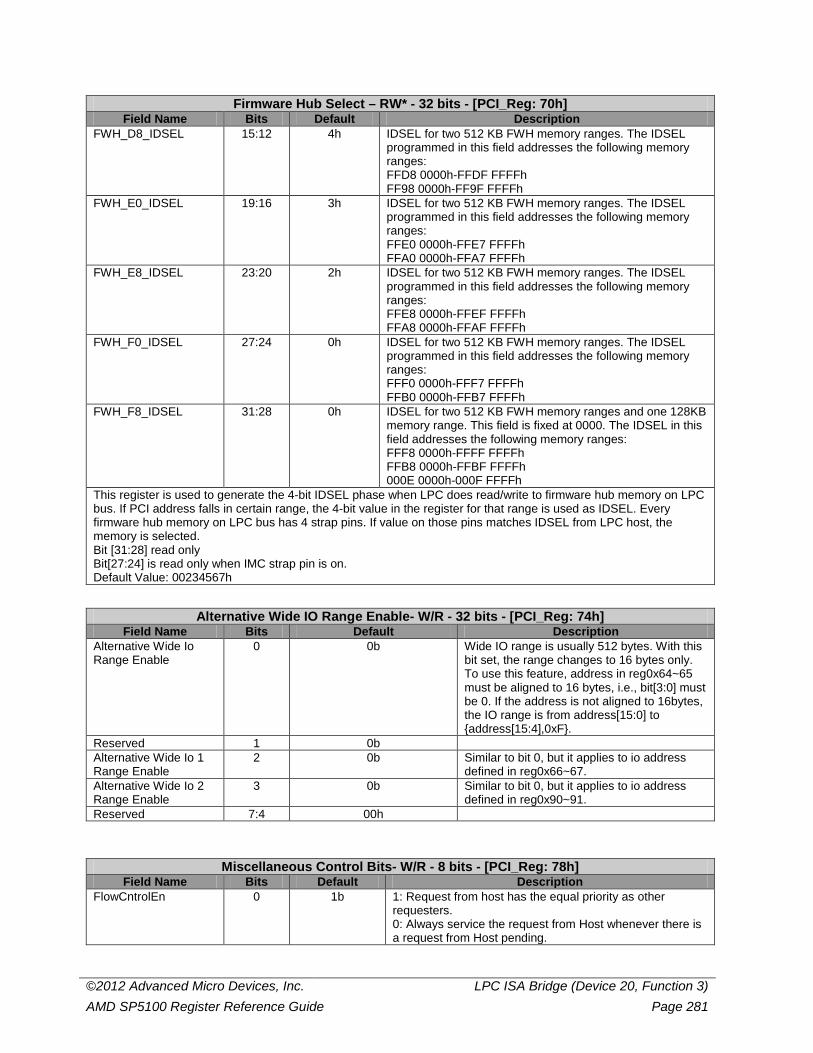
©2012 Advanced Micro Devices, Inc. LPC ISA Bridge (Device 20, Function 3) AMD SP5100 Register Reference Guide Page 281
Firmware Hub Select – RW* - 32 bits - [PCI_Reg: 70h] Field Name Bits Default Description
FWH_D8_IDSEL 15:12 4h IDSEL for two 512 KB FWH memory ranges. The IDSEL programmed in this field addresses the following memory ranges: FFD8 0000h-FFDF FFFFh FF98 0000h-FF9F FFFFh
FWH_E0_IDSEL 19:16 3h IDSEL for two 512 KB FWH memory ranges. The IDSEL programmed in this field addresses the following memory ranges: FFE0 0000h-FFE7 FFFFh FFA0 0000h-FFA7 FFFFh
FWH_E8_IDSEL 23:20 2h IDSEL for two 512 KB FWH memory ranges. The IDSEL programmed in this field addresses the following memory ranges: FFE8 0000h-FFEF FFFFh FFA8 0000h-FFAF FFFFh
FWH_F0_IDSEL 27:24 0h IDSEL for two 512 KB FWH memory ranges. The IDSEL programmed in this field addresses the following memory ranges: FFF0 0000h-FFF7 FFFFh FFB0 0000h-FFB7 FFFFh
FWH_F8_IDSEL 31:28 0h IDSEL for two 512 KB FWH memory ranges and one 128KB memory range. This field is fixed at 0000. The IDSEL in this field addresses the following memory ranges: FFF8 0000h-FFFF FFFFh FFB8 0000h-FFBF FFFFh 000E 0000h-000F FFFFh
This register is used to generate the 4-bit IDSEL phase when LPC does read/write to firmware hub memory on LPC bus. If PCI address falls in certain range, the 4-bit value in the register for that range is used as IDSEL. Every firmware hub memory on LPC bus has 4 strap pins. If value on those pins matches IDSEL from LPC host, the memory is selected. Bit [31:28] read only Bit[27:24] is read only when IMC strap pin is on. Default Value: 00234567h
Alternative Wide IO Range Enable- W/R - 32 bits - [PCI_Reg: 74h] Field Name Bits Default Description
Alternative Wide Io Range Enable
0 0b Wide IO range is usually 512 bytes. With this bit set, the range changes to 16 bytes only. To use this feature, address in reg0x64~65 must be aligned to 16 bytes, i.e., bit[3:0] must be 0. If the address is not aligned to 16bytes, the IO range is from address[15:0] to {address[15:4],0xF}.
Reserved 1 0b Alternative Wide Io 1 Range Enable
2 0b Similar to bit 0, but it applies to io address defined in reg0x66~67.
Alternative Wide Io 2 Range Enable
3 0b Similar to bit 0, but it applies to io address defined in reg0x90~91.
Reserved 7:4 00h
Miscellaneous Control Bits- W/R - 8 bits - [PCI_Reg: 78h] Field Name Bits Default Description
FlowCntrolEn 0 1b 1: Request from host has the equal priority as other requesters. 0: Always service the request from Host whenever there is a request from Host pending.
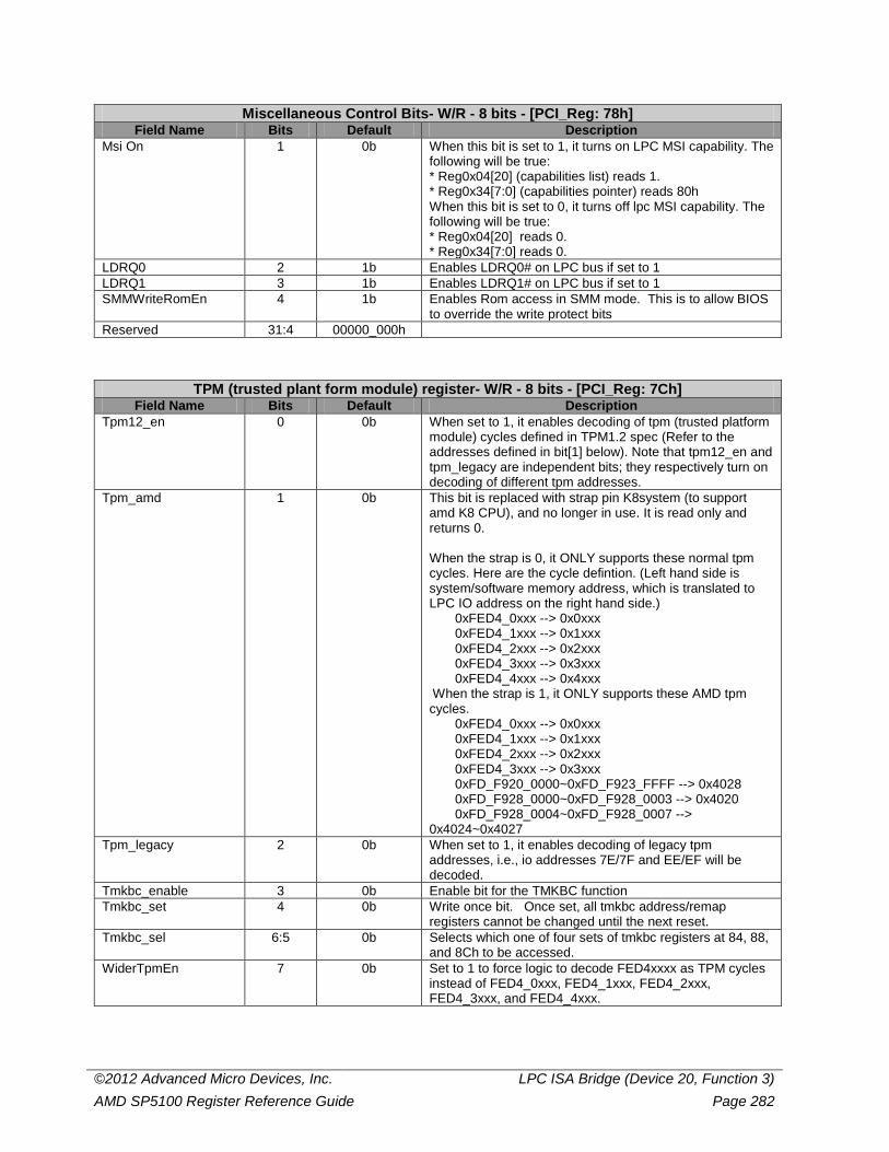
©2012 Advanced Micro Devices, Inc. LPC ISA Bridge (Device 20, Function 3) AMD SP5100 Register Reference Guide Page 282
Miscellaneous Control Bits- W/R - 8 bits - [PCI_Reg: 78h] Field Name Bits Default Description
Msi On 1 0b When this bit is set to 1, it turns on LPC MSI capability. The following will be true: * Reg0x04[20] (capabilities list) reads 1. * Reg0x34[7:0] (capabilities pointer) reads 80h When this bit is set to 0, it turns off lpc MSI capability. The following will be true: * Reg0x04[20] reads 0. * Reg0x34[7:0] reads 0.
LDRQ0 2 1b Enables LDRQ0# on LPC bus if set to 1 LDRQ1 3 1b Enables LDRQ1# on LPC bus if set to 1 SMMWriteRomEn 4 1b Enables Rom access in SMM mode. This is to allow BIOS
to override the write protect bits Reserved 31:4 00000_000h
TPM (trusted plant form module) register- W/R - 8 bits - [PCI_Reg: 7Ch] Field Name Bits Default Description
Tpm12_en 0 0b When set to 1, it enables decoding of tpm (trusted platform module) cycles defined in TPM1.2 spec (Refer to the addresses defined in bit[1] below). Note that tpm12_en and tpm_legacy are independent bits; they respectively turn on decoding of different tpm addresses.
Tpm_amd 1 0b This bit is replaced with strap pin K8system (to support amd K8 CPU), and no longer in use. It is read only and returns 0. When the strap is 0, it ONLY supports these normal tpm cycles. Here are the cycle defintion. (Left hand side is system/software memory address, which is translated to LPC IO address on the right hand side.) 0xFED4_0xxx --> 0x0xxx 0xFED4_1xxx --> 0x1xxx 0xFED4_2xxx --> 0x2xxx 0xFED4_3xxx --> 0x3xxx 0xFED4_4xxx --> 0x4xxx When the strap is 1, it ONLY supports these AMD tpm cycles. 0xFED4_0xxx --> 0x0xxx 0xFED4_1xxx --> 0x1xxx 0xFED4_2xxx --> 0x2xxx 0xFED4_3xxx --> 0x3xxx 0xFD_F920_0000~0xFD_F923_FFFF --> 0x4028 0xFD_F928_0000~0xFD_F928_0003 --> 0x4020 0xFD_F928_0004~0xFD_F928_0007 --> 0x4024~0x4027
Tpm_legacy 2 0b When set to 1, it enables decoding of legacy tpm addresses, i.e., io addresses 7E/7F and EE/EF will be decoded.
Tmkbc_enable 3 0b Enable bit for the TMKBC function Tmkbc_set 4 0b Write once bit. Once set, all tmkbc address/remap
registers cannot be changed until the next reset. Tmkbc_sel 6:5 0b Selects which one of four sets of tmkbc registers at 84, 88,
and 8Ch to be accessed. WiderTpmEn 7 0b Set to 1 to force logic to decode FED4xxxx as TPM cycles
instead of FED4_0xxx, FED4_1xxx, FED4_2xxx, FED4_3xxx, and FED4_4xxx.
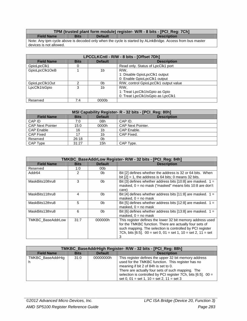
©2012 Advanced Micro Devices, Inc. LPC ISA Bridge (Device 20, Function 3) AMD SP5100 Register Reference Guide Page 283
TPM (trusted plant form module) register- W/R - 8 bits - [PCI_Reg: 7Ch] Field Name Bits Default Description
Note: Any tpm cycle above is decoded only when the cycle is started by ALinkBridge. Access from bus master devices is not allowed.
LPCCLKCntl - R/W - 8 bits - [Offset 7Dh] Field Name Bits Default Description
GpioLpcClk1 0 Read only. Status of LpcClk1 port GpioLpcClk1OeB 1 1b R/W,
1: Disable GpioLpcClk1 output 0: Enable GpioLpcClk1 output
GpioLpcClk1Out 2 0b R/W, control GpioLpcClk1 output value LpcClk1IsGpio 3 1b R/W,
1: Treat LpcClk1IsGpio as Gpio 0: Treat LpcClk1IsGpio as LpcClk1
Reserved 7:4 0000b
MSI Capability Register- R - 32 bits - [PCI_Reg: 80h] Field Name Bits Default Description
CAP ID 7:0 08h CAP ID. CAP Next Pointer 15:0 0000h CAP Next Pointer. CAP Enable 16 1b CAP Enable. CAP Fixed 17 1b CAP Fixed. Reserved 26:18 0b CAP Type 31:27 15h CAP Type.
TMKBC_BaseAddrLow Register- R/W - 32 bits - [PCI_Reg: 84h] Field Name Bits Default Description
Reserved 1:0 00b Addr64 2 0b Bit [2] defines whether the address is 32 or 64 bits. When
bit [2] = 1, the address is 64 bits; 0 means 32 bits. MaskBits10thru8 3 0b Bit [3] defines whether address bits [10:8] are masked. 1 =
masked, 0 = no mask (“masked” means bits 10:8 are don’t care)
MaskBits11thru8 4 0b Bit [4] defines whether address bits [11:8] are masked. 1 = masked, 0 = no mask
MaskBits12thru8 5 0b Bit [5] defines whether address bits [12:8] are masked. 1 = masked, 0 = no mask
MaskBits13thru8 6 0b Bit [6] defines whether address bits [13:8] are masked. 1 = masked, 0 = no mask
TMKBC_BaseAddrLow 31:7 000000h This register defines the lower 32 bit memory address used for the TMKBC function. There are actually four sets of such mapping. The selection is controlled by PCI register 7Ch, bits [6:5]. 00 = set 0, 01 = set 1, 10 = set 2, 11 = set 3
TMKBC_BaseAddrHigh Register- R/W - 32 bits - [PCI_Reg: 88h] Field Name Bits Default Description
TMKBC_BaseAddrHigh
31:0 00000000h This register defines the upper 32 bit memory address used for the TMKBC function. This register has no meaning if bit 2 of 84h is set to 0. There are actually four sets of such mapping. The selection is controlled by PCI register 7Ch, bits [6:5]. 00 = set 0, 01 = set 1, 10 = set 2, 11 = set 3
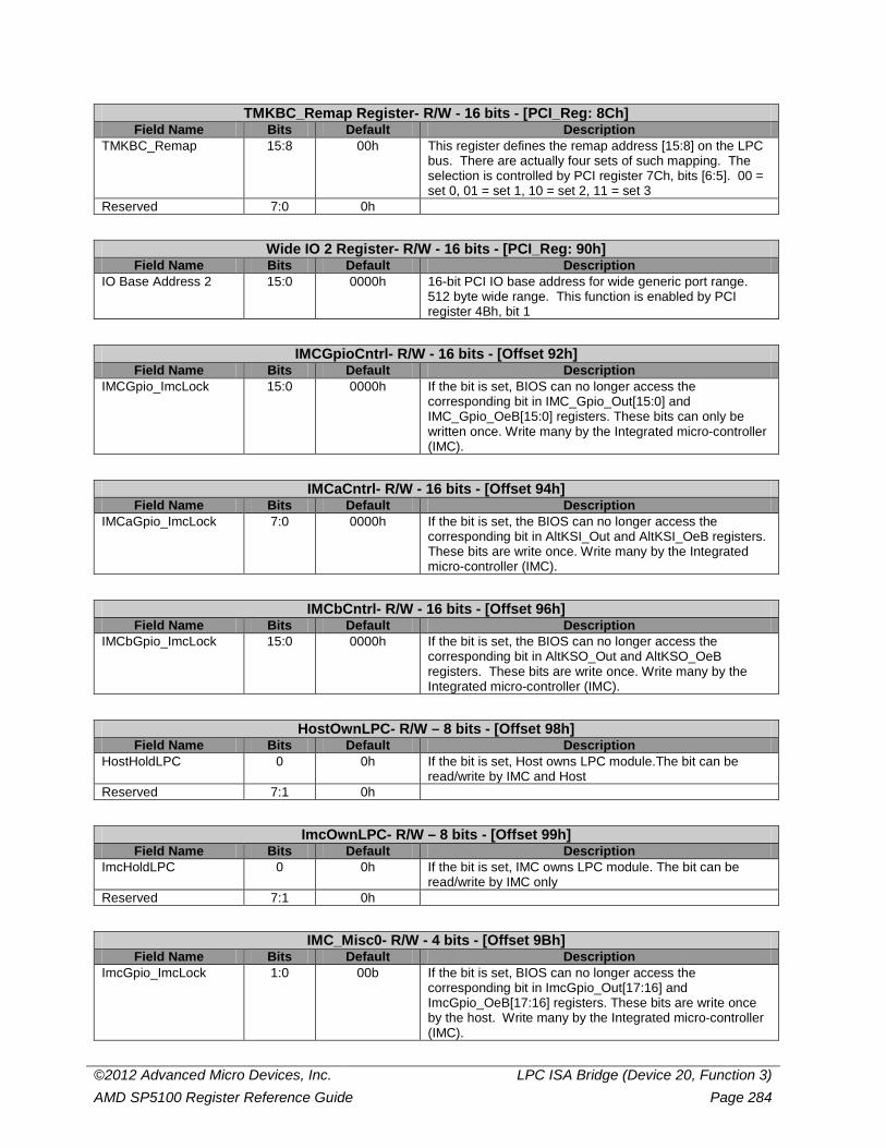
©2012 Advanced Micro Devices, Inc. LPC ISA Bridge (Device 20, Function 3) AMD SP5100 Register Reference Guide Page 284
TMKBC_Remap Register- R/W - 16 bits - [PCI_Reg: 8Ch] Field Name Bits Default Description
TMKBC_Remap 15:8 00h This register defines the remap address [15:8] on the LPC bus. There are actually four sets of such mapping. The selection is controlled by PCI register 7Ch, bits [6:5]. 00 = set 0, 01 = set 1, 10 = set 2, 11 = set 3
Reserved 7:0 0h
Wide IO 2 Register- R/W - 16 bits - [PCI_Reg: 90h] Field Name Bits Default Description
IO Base Address 2 15:0 0000h 16-bit PCI IO base address for wide generic port range. 512 byte wide range. This function is enabled by PCI register 4Bh, bit 1
IMCGpioCntrl- R/W - 16 bits - [Offset 92h] Field Name Bits Default Description
IMCGpio_ImcLock 15:0 0000h If the bit is set, BIOS can no longer access the corresponding bit in IMC_Gpio_Out[15:0] and IMC_Gpio_OeB[15:0] registers. These bits can only be written once. Write many by the Integrated micro-controller (IMC).
IMCaCntrl- R/W - 16 bits - [Offset 94h] Field Name Bits Default Description
IMCaGpio_ImcLock 7:0 0000h If the bit is set, the BIOS can no longer access the corresponding bit in AltKSI_Out and AltKSI_OeB registers. These bits are write once. Write many by the Integrated micro-controller (IMC).
IMCbCntrl- R/W - 16 bits - [Offset 96h] Field Name Bits Default Description
IMCbGpio_ImcLock 15:0 0000h If the bit is set, the BIOS can no longer access the corresponding bit in AltKSO_Out and AltKSO_OeB registers. These bits are write once. Write many by the Integrated micro-controller (IMC).
HostOwnLPC- R/W – 8 bits - [Offset 98h] Field Name Bits Default Description
HostHoldLPC 0 0h If the bit is set, Host owns LPC module.The bit can be read/write by IMC and Host
Reserved 7:1 0h
ImcOwnLPC- R/W – 8 bits - [Offset 99h] Field Name Bits Default Description
ImcHoldLPC 0 0h If the bit is set, IMC owns LPC module. The bit can be read/write by IMC only
Reserved 7:1 0h
IMC_Misc0- R/W - 4 bits - [Offset 9Bh] Field Name Bits Default Description
ImcGpio_ImcLock 1:0 00b If the bit is set, BIOS can no longer access the corresponding bit in ImcGpio_Out[17:16] and ImcGpio_OeB[17:16] registers. These bits are write once by the host. Write many by the Integrated micro-controller (IMC).
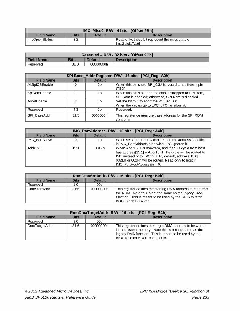
©2012 Advanced Micro Devices, Inc. LPC ISA Bridge (Device 20, Function 3) AMD SP5100 Register Reference Guide Page 285
IMC_Misc0- R/W - 4 bits - [Offset 9Bh] Field Name Bits Default Description
ImcGpio_Status 3:2 ---- Read only, those bit represent the input state of ImcGpio[17,16]
Reserved – R/W - 32 bits - [Offset 9Ch] Field Name Bits Default Description Reserved 31:0 00000000h
SPI Base_Addr Register- R/W - 16 bits - [PCI_Reg: A0h] Field Name Bits Default Description
AltSpiCSEnable 0 0b When this bit is set, SPI_CS# is routed to a different pin (TBD)
SpiRomEnable 1 1b When this bit is set and the chip is strapped to SPI Rom, SPI Rom is enabled; otherwise, SPI Rom is disabled.
AbortEnable 2 0b Set the bit to 1 to abort the PCI request. When the cycles go to LPC, LPC will abort it.
Reserved 4:3 0b Reserved. SPI_BaseAddr 31:5 0000000h This register defines the base address for the SPI ROM
controller
IMC_PortAddress- R/W - 16 bits - [PCI_Reg: A4h] Field Name Bits Default Description
IMC_PortActive 0 1b When sets it to 1, LPC can decode the address specified in IMC_PortAddress otherwise LPC ignores it.
Addr15_1 15:1 0017h When Addr15_1 is non-zero, and if an IO cycle from host has address[15:1] = Addr15_1, the cycle will be routed to IMC instead of to LPC bus. By default, address[15:0] = 002Eh or 002Fh will be routed. Read-only to host if IMC_PortHostAccessEn = 0.
RomDmaSrcAddr- R/W - 16 bits - [PCI_Reg: B0h] Field Name Bits Default Description
Reserved 1:0 00b DmaStartAddr 31:6 00000000h This register defines the starting DMA address to read from
the ROM. Note this is not the same as the legacy DMA function. This is meant to be used by the BIOS to fetch BOOT codes quicker.
RomDmaTargetAddr- R/W - 16 bits - [PCI_Reg: B4h] Field Name Bits Default Description
Reserved 5:0 00b DmaTargetAddr 31:6 00000000h This register defines the target DMA address to be written
in the system memory. Note this is not the same as the legacy DMA function. This is meant to be used by the BIOS to fetch BOOT codes quicker.
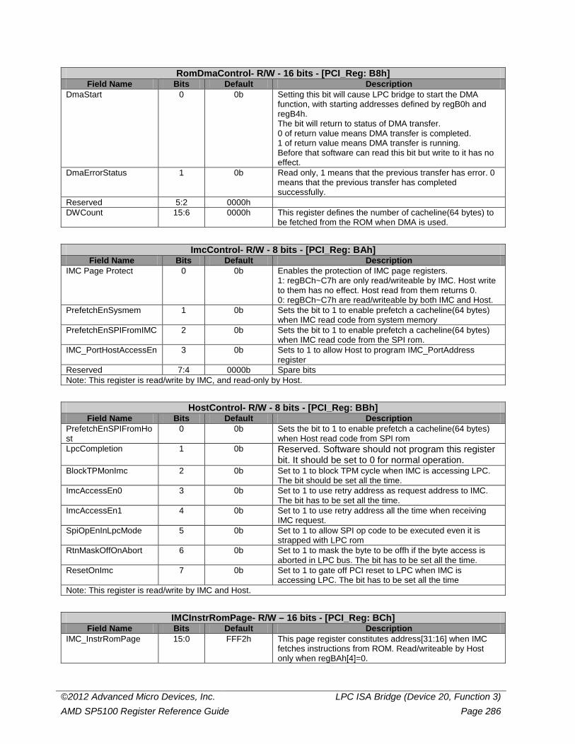
©2012 Advanced Micro Devices, Inc. LPC ISA Bridge (Device 20, Function 3) AMD SP5100 Register Reference Guide Page 286
RomDmaControl- R/W - 16 bits - [PCI_Reg: B8h] Field Name Bits Default Description
DmaStart 0 0b Setting this bit will cause LPC bridge to start the DMA function, with starting addresses defined by regB0h and regB4h. The bit will return to status of DMA transfer. 0 of return value means DMA transfer is completed. 1 of return value means DMA transfer is running. Before that software can read this bit but write to it has no effect.
DmaErrorStatus 1 0b Read only, 1 means that the previous transfer has error. 0 means that the previous transfer has completed successfully.
Reserved 5:2 0000h DWCount 15:6 0000h This register defines the number of cacheline(64 bytes) to
be fetched from the ROM when DMA is used.
ImcControl- R/W - 8 bits - [PCI_Reg: BAh] Field Name Bits Default Description
IMC Page Protect 0 0b Enables the protection of IMC page registers. 1: regBCh~C7h are only read/writeable by IMC. Host write to them has no effect. Host read from them returns 0. 0: regBCh~C7h are read/writeable by both IMC and Host.
PrefetchEnSysmem 1 0b Sets the bit to 1 to enable prefetch a cacheline(64 bytes) when IMC read code from system memory
PrefetchEnSPIFromIMC 2 0b Sets the bit to 1 to enable prefetch a cacheline(64 bytes) when IMC read code from the SPI rom.
IMC_PortHostAccessEn 3 0b Sets to 1 to allow Host to program IMC_PortAddress register
Reserved 7:4 0000b Spare bits Note: This register is read/write by IMC, and read-only by Host.
HostControl- R/W - 8 bits - [PCI_Reg: BBh] Field Name Bits Default Description
PrefetchEnSPIFromHost
0 0b Sets the bit to 1 to enable prefetch a cacheline(64 bytes) when Host read code from SPI rom
LpcCompletion 1 0b Reserved. Software should not program this register bit. It should be set to 0 for normal operation.
BlockTPMonImc 2 0b Set to 1 to block TPM cycle when IMC is accessing LPC. The bit should be set all the time.
ImcAccessEn0 3 0b Set to 1 to use retry address as request address to IMC. The bit has to be set all the time.
ImcAccessEn1 4 0b Set to 1 to use retry address all the time when receiving IMC request.
SpiOpEnInLpcMode 5 0b Set to 1 to allow SPI op code to be executed even it is strapped with LPC rom
RtnMaskOffOnAbort 6 0b Set to 1 to mask the byte to be offh if the byte access is aborted in LPC bus. The bit has to be set all the time.
ResetOnImc 7 0b Set to 1 to gate off PCI reset to LPC when IMC is accessing LPC. The bit has to be set all the time
Note: This register is read/write by IMC and Host.
IMCInstrRomPage- R/W – 16 bits - [PCI_Reg: BCh] Field Name Bits Default Description
IMC_InstrRomPage 15:0 FFF2h This page register constitutes address[31:16] when IMC fetches instructions from ROM. Read/writeable by Host only when regBAh[4]=0.
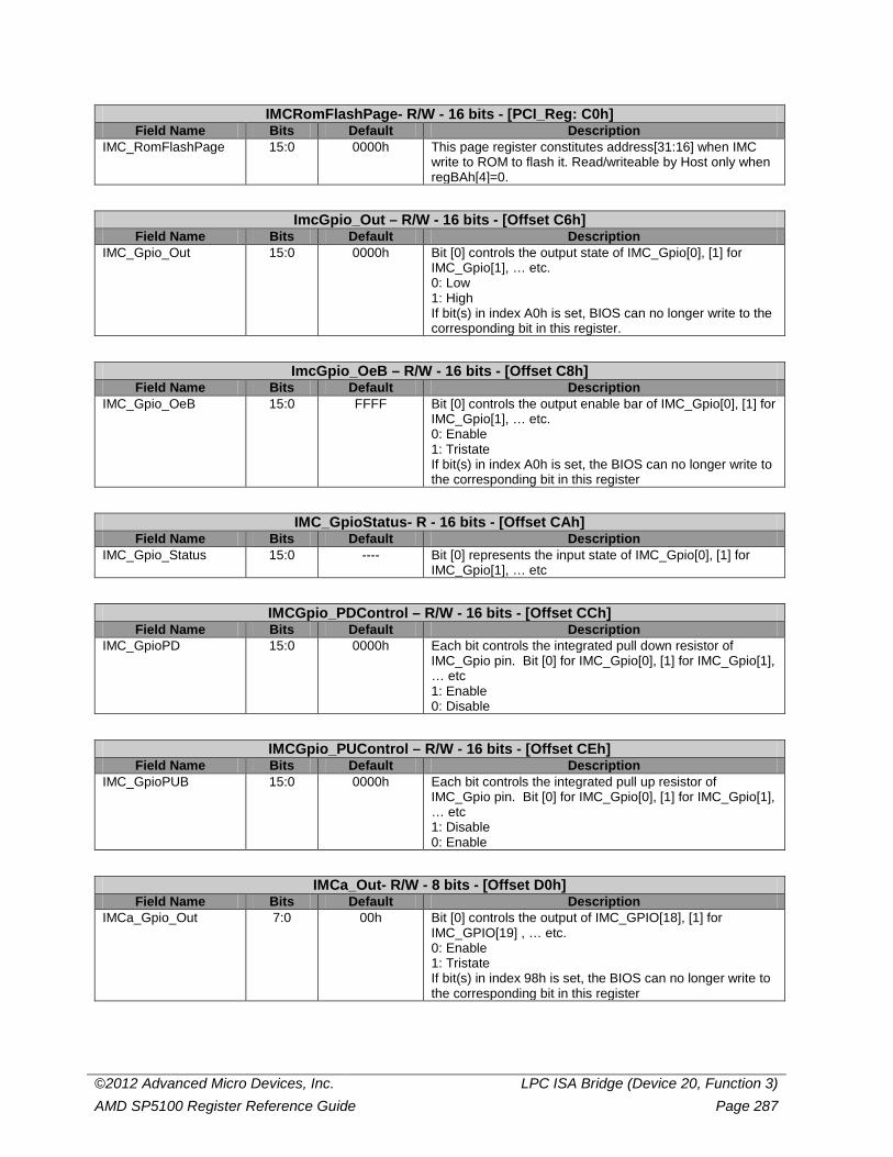
©2012 Advanced Micro Devices, Inc. LPC ISA Bridge (Device 20, Function 3) AMD SP5100 Register Reference Guide Page 287
IMCRomFlashPage- R/W - 16 bits - [PCI_Reg: C0h] Field Name Bits Default Description
IMC_RomFlashPage 15:0 0000h This page register constitutes address[31:16] when IMC write to ROM to flash it. Read/writeable by Host only when regBAh[4]=0.
ImcGpio_Out – R/W - 16 bits - [Offset C6h] Field Name Bits Default Description
IMC_Gpio_Out 15:0 0000h Bit [0] controls the output state of IMC_Gpio[0], [1] for IMC_Gpio[1], … etc. 0: Low 1: High If bit(s) in index A0h is set, BIOS can no longer write to the corresponding bit in this register.
ImcGpio_OeB – R/W - 16 bits - [Offset C8h] Field Name Bits Default Description
IMC_Gpio_OeB 15:0 FFFF Bit [0] controls the output enable bar of IMC_Gpio[0], [1] for IMC_Gpio[1], … etc. 0: Enable 1: Tristate If bit(s) in index A0h is set, the BIOS can no longer write to the corresponding bit in this register
IMC_GpioStatus- R - 16 bits - [Offset CAh] Field Name Bits Default Description
IMC_Gpio_Status 15:0 ---- Bit [0] represents the input state of IMC_Gpio[0], [1] for IMC_Gpio[1], … etc
IMCGpio_PDControl – R/W - 16 bits - [Offset CCh] Field Name Bits Default Description
IMC_GpioPD 15:0 0000h Each bit controls the integrated pull down resistor of IMC_Gpio pin. Bit [0] for IMC_Gpio[0], [1] for IMC_Gpio[1], … etc 1: Enable 0: Disable
IMCGpio_PUControl – R/W - 16 bits - [Offset CEh] Field Name Bits Default Description
IMC_GpioPUB 15:0 0000h Each bit controls the integrated pull up resistor of IMC_Gpio pin. Bit [0] for IMC_Gpio[0], [1] for IMC_Gpio[1], … etc 1: Disable 0: Enable
IMCa_Out- R/W - 8 bits - [Offset D0h] Field Name Bits Default Description
IMCa_Gpio_Out 7:0 00h Bit [0] controls the output of IMC_GPIO[18], [1] for IMC_GPIO[19] , … etc. 0: Enable 1: Tristate If bit(s) in index 98h is set, the BIOS can no longer write to the corresponding bit in this register
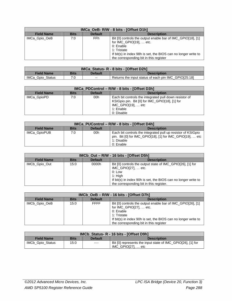
©2012 Advanced Micro Devices, Inc. LPC ISA Bridge (Device 20, Function 3) AMD SP5100 Register Reference Guide Page 288
IMCa_OeB- R/W - 8 bits - [Offset D1h] Field Name Bits Default Description
IMCa_Gpio_OeB 7:0 FFh Bit [0] controls the output enable bar of IMC_GPIO[18], [1] for IMC_GPIO[19], … etc. 0: Enable 1: Tristate If bit(s) in index 98h is set, the BIOS can no longer write to the corresponding bit in this register
IMCa_Status- R - 8 bits - [Offset D2h] Field Name Bits Default Description
IMCa_Gpio_Status 7:0 -- Returns the input status of each pin IMC_GPIO[25:18]
IMCa_PDControl – R/W - 8 bits - [Offset D3h] Field Name Bits Default Description
IMCa_GpioPD 7:0 00h Each bit controls the integrated pull down resistor of KSIGpio pin. Bit [0] for IMC_GPIO[18], [1] for IMC_GPIO[19], … etc 1: Enable 0: Disable
IMCa_PUControl – R/W - 8 bits - [Offset D4h] Field Name Bits Default Description
IMCa_GpioPUB 7:0 00h Each bit controls the integrated pull up resistor of KSIGpio pin. Bit [0] for IMC_GPIO[18], [1] for IMC_GPIO[19], … etc 1: Disable 0: Enable
IMCb_Out – R/W - 16 bits - [Offset D5h] Field Name Bits Default Description
IMCb_Gpio_Out 15:0 0000h Bit [0] controls the output state of IMC_GPIO[26], [1] for IMC_GPIO[27], … etc. 0: Low 1: High If bit(s) in index 90h is set, the BIOS can no longer write to the corresponding bit in this register.
IMCb_OeB – R/W - 16 bits - [Offset D7h] Field Name Bits Default Description
IMCb_Gpio_OeB 15:0 FFFF Bit [0] controls the output enable bar of IMC_GPIO[26], [1] for IMC_GPIO[27], … etc. 0: Enable 1: Tristate If bit(s) in index 90h is set, the BIOS can no longer write to the corresponding bit in this register
IMCb_Status- R - 16 bits - [Offset D9h] Field Name Bits Default Description
IMCb_Gpio_Status 15:0 ---- Bit [0] represents the input state of IMC_GPIO[26], [1] for IMC_GPIO[27], … etc
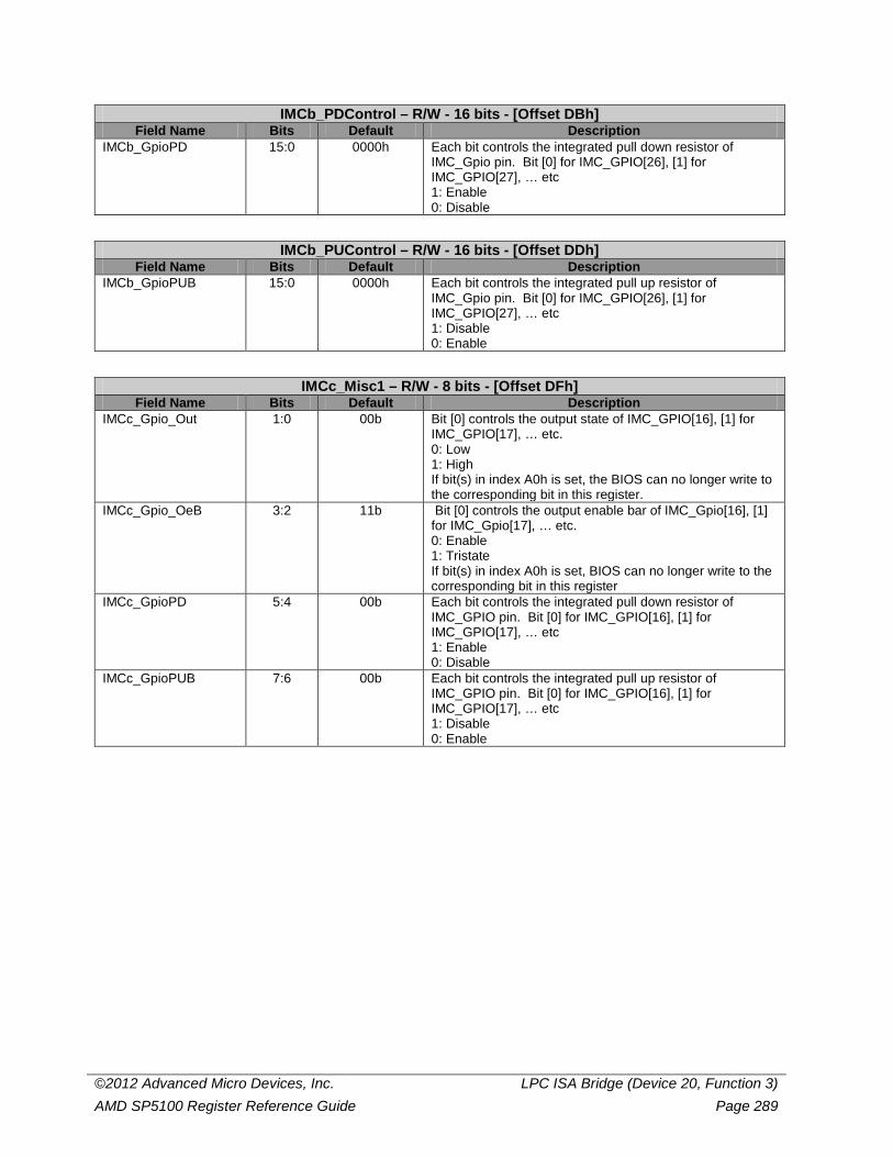
©2012 Advanced Micro Devices, Inc. LPC ISA Bridge (Device 20, Function 3) AMD SP5100 Register Reference Guide Page 289
IMCb_PDControl – R/W - 16 bits - [Offset DBh] Field Name Bits Default Description
IMCb_GpioPD 15:0 0000h Each bit controls the integrated pull down resistor of IMC_Gpio pin. Bit [0] for IMC_GPIO[26], [1] for IMC_GPIO[27], … etc 1: Enable 0: Disable
IMCb_PUControl – R/W - 16 bits - [Offset DDh] Field Name Bits Default Description
IMCb_GpioPUB 15:0 0000h Each bit controls the integrated pull up resistor of IMC_Gpio pin. Bit [0] for IMC_GPIO[26], [1] for IMC_GPIO[27], … etc 1: Disable 0: Enable
IMCc_Misc1 – R/W - 8 bits - [Offset DFh] Field Name Bits Default Description
IMCc_Gpio_Out 1:0 00b Bit [0] controls the output state of IMC_GPIO[16], [1] for IMC_GPIO[17], … etc. 0: Low 1: High If bit(s) in index A0h is set, the BIOS can no longer write to the corresponding bit in this register.
IMCc_Gpio_OeB 3:2 11b Bit [0] controls the output enable bar of IMC_Gpio[16], [1] for IMC_Gpio[17], … etc. 0: Enable 1: Tristate If bit(s) in index A0h is set, BIOS can no longer write to the corresponding bit in this register
IMCc_GpioPD 5:4 00b Each bit controls the integrated pull down resistor of IMC_GPIO pin. Bit [0] for IMC_GPIO[16], [1] for IMC_GPIO[17], … etc 1: Enable 0: Disable
IMCc_GpioPUB 7:6 00b Each bit controls the integrated pull up resistor of IMC_GPIO pin. Bit [0] for IMC_GPIO[16], [1] for IMC_GPIO[17], … etc 1: Disable 0: Enable
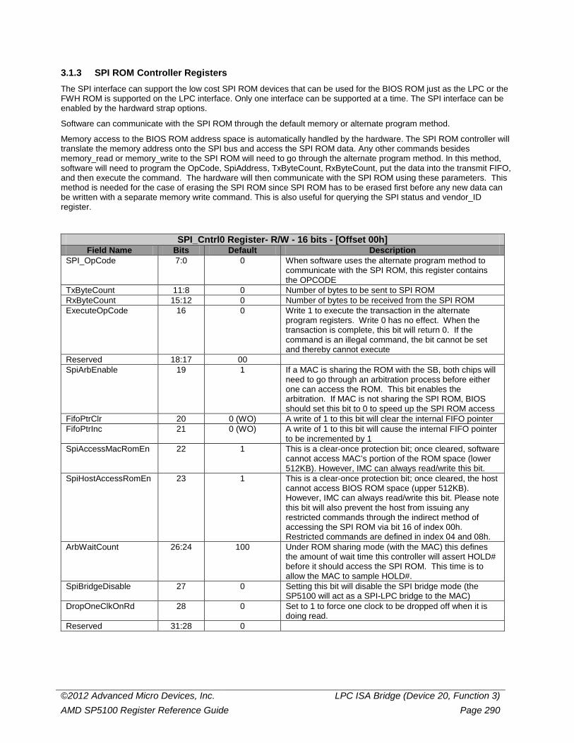
©2012 Advanced Micro Devices, Inc. LPC ISA Bridge (Device 20, Function 3) AMD SP5100 Register Reference Guide Page 290
3.1.3 SPI ROM Controller Registers The SPI interface can support the low cost SPI ROM devices that can be used for the BIOS ROM just as the LPC or the FWH ROM is supported on the LPC interface. Only one interface can be supported at a time. The SPI interface can be enabled by the hardward strap options.
Software can communicate with the SPI ROM through the default memory or alternate program method.
Memory access to the BIOS ROM address space is automatically handled by the hardware. The SPI ROM controller will translate the memory address onto the SPI bus and access the SPI ROM data. Any other commands besides memory_read or memory_write to the SPI ROM will need to go through the alternate program method. In this method, software will need to program the OpCode, SpiAddress, TxByteCount, RxByteCount, put the data into the transmit FIFO, and then execute the command. The hardware will then communicate with the SPI ROM using these parameters. This method is needed for the case of erasing the SPI ROM since SPI ROM has to be erased first before any new data can be written with a separate memory write command. This is also useful for querying the SPI status and vendor_ID register.
SPI_Cntrl0 Register- R/W - 16 bits - [Offset 00h] Field Name Bits Default Description
SPI_OpCode 7:0 0 When software uses the alternate program method to communicate with the SPI ROM, this register contains the OPCODE
TxByteCount 11:8 0 Number of bytes to be sent to SPI ROM RxByteCount 15:12 0 Number of bytes to be received from the SPI ROM ExecuteOpCode 16 0 Write 1 to execute the transaction in the alternate
program registers. Write 0 has no effect. When the transaction is complete, this bit will return 0. If the command is an illegal command, the bit cannot be set and thereby cannot execute
Reserved 18:17 00 SpiArbEnable 19 1 If a MAC is sharing the ROM with the SB, both chips will
need to go through an arbitration process before either one can access the ROM. This bit enables the arbitration. If MAC is not sharing the SPI ROM, BIOS should set this bit to 0 to speed up the SPI ROM access
FifoPtrClr 20 0 (WO) A write of 1 to this bit will clear the internal FIFO pointer FifoPtrInc 21 0 (WO) A write of 1 to this bit will cause the internal FIFO pointer
to be incremented by 1 SpiAccessMacRomEn 22 1 This is a clear-once protection bit; once cleared, software
cannot access MAC’s portion of the ROM space (lower 512KB). However, IMC can always read/write this bit.
SpiHostAccessRomEn 23 1 This is a clear-once protection bit; once cleared, the host cannot access BIOS ROM space (upper 512KB). However, IMC can always read/write this bit. Please note this bit will also prevent the host from issuing any restricted commands through the indirect method of accessing the SPI ROM via bit 16 of index 00h. Restricted commands are defined in index 04 and 08h.
ArbWaitCount 26:24 100 Under ROM sharing mode (with the MAC) this defines the amount of wait time this controller will assert HOLD# before it should access the SPI ROM. This time is to allow the MAC to sample HOLD#.
SpiBridgeDisable 27 0 Setting this bit will disable the SPI bridge mode (the SP5100 will act as a SPI-LPC bridge to the MAC)
DropOneClkOnRd 28 0 Set to 1 to force one clock to be dropped off when it is doing read.
Reserved 31:28 0
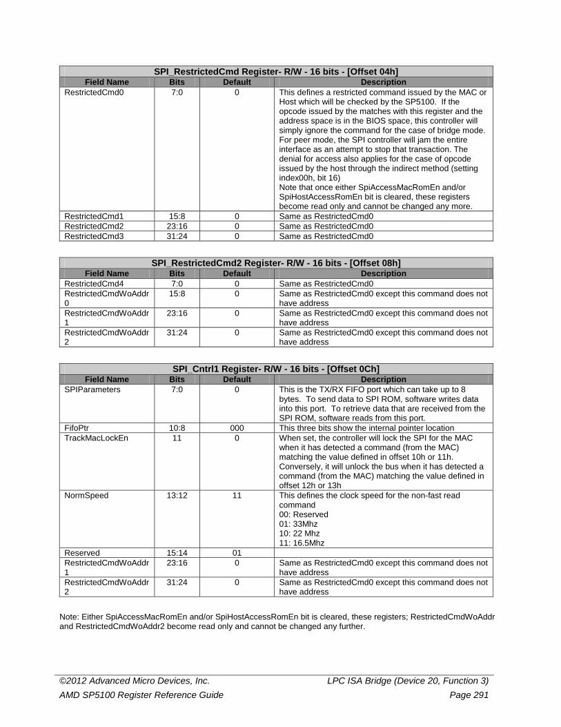
©2012 Advanced Micro Devices, Inc. LPC ISA Bridge (Device 20, Function 3) AMD SP5100 Register Reference Guide Page 291
SPI_RestrictedCmd Register- R/W - 16 bits - [Offset 04h] Field Name Bits Default Description
RestrictedCmd0 7:0 0 This defines a restricted command issued by the MAC or Host which will be checked by the SP5100. If the opcode issued by the matches with this register and the address space is in the BIOS space, this controller will simply ignore the command for the case of bridge mode. For peer mode, the SPI controller will jam the entire interface as an attempt to stop that transaction. The denial for access also applies for the case of opcode issued by the host through the indirect method (setting index00h, bit 16) Note that once either SpiAccessMacRomEn and/or SpiHostAccessRomEn bit is cleared, these registers become read only and cannot be changed any more.
RestrictedCmd1 15:8 0 Same as RestrictedCmd0 RestrictedCmd2 23:16 0 Same as RestrictedCmd0 RestrictedCmd3 31:24 0 Same as RestrictedCmd0
SPI_RestrictedCmd2 Register- R/W - 16 bits - [Offset 08h] Field Name Bits Default Description
RestrictedCmd4 7:0 0 Same as RestrictedCmd0 RestrictedCmdWoAddr0
15:8 0 Same as RestrictedCmd0 except this command does not have address
RestrictedCmdWoAddr1
23:16 0 Same as RestrictedCmd0 except this command does not have address
RestrictedCmdWoAddr2
31:24 0 Same as RestrictedCmd0 except this command does not have address
SPI_Cntrl1 Register- R/W - 16 bits - [Offset 0Ch] Field Name Bits Default Description
SPIParameters 7:0 0 This is the TX/RX FIFO port which can take up to 8 bytes. To send data to SPI ROM, software writes data into this port. To retrieve data that are received from the SPI ROM, software reads from this port.
FifoPtr 10:8 000 This three bits show the internal pointer location TrackMacLockEn 11 0 When set, the controller will lock the SPI for the MAC
when it has detected a command (from the MAC) matching the value defined in offset 10h or 11h. Conversely, it will unlock the bus when it has detected a command (from the MAC) matching the value defined in offset 12h or 13h
NormSpeed 13:12 11 This defines the clock speed for the non-fast read command 00: Reserved 01: 33Mhz 10: 22 Mhz 11: 16.5Mhz
Reserved 15:14 01 RestrictedCmdWoAddr1
23:16 0 Same as RestrictedCmd0 except this command does not have address
RestrictedCmdWoAddr2
31:24 0 Same as RestrictedCmd0 except this command does not have address
Note: Either SpiAccessMacRomEn and/or SpiHostAccessRomEn bit is cleared, these registers; RestrictedCmdWoAddr and RestrictedCmdWoAddr2 become read only and cannot be changed any further.
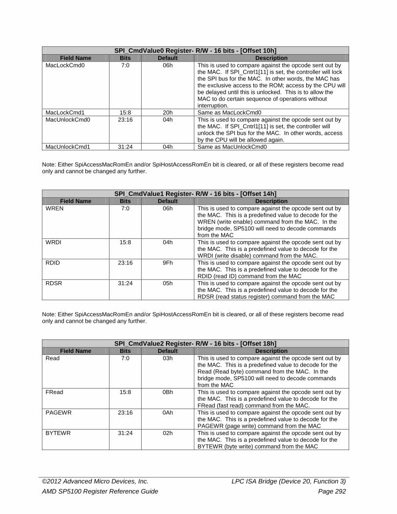
©2012 Advanced Micro Devices, Inc. LPC ISA Bridge (Device 20, Function 3) AMD SP5100 Register Reference Guide Page 292
SPI_CmdValue0 Register- R/W - 16 bits - [Offset 10h] Field Name Bits Default Description
MacLockCmd0 7:0 06h This is used to compare against the opcode sent out by the MAC. If SPI_Cntrl1[11] is set, the controller will lock the SPI bus for the MAC. In other words, the MAC has the exclusive access to the ROM; access by the CPU will be delayed until this is unlocked. This is to allow the MAC to do certain sequence of operations without interruption.
MacLockCmd1 15:8 20h Same as MacLockCmd0 MacUnlockCmd0 23:16 04h This is used to compare against the opcode sent out by
the MAC. If SPI_Cntrl1[11] is set, the controller will unlock the SPI bus for the MAC. In other words, access by the CPU will be allowed again.
MacUnlockCmd1 31:24 04h Same as MacUnlockCmd0
Note: Either SpiAccessMacRomEn and/or SpiHostAccessRomEn bit is cleared, or all of these registers become read only and cannot be changed any further.
SPI_CmdValue1 Register- R/W - 16 bits - [Offset 14h] Field Name Bits Default Description
WREN 7:0 06h This is used to compare against the opcode sent out by the MAC. This is a predefined value to decode for the WREN (write enable) command from the MAC. In the bridge mode, SP5100 will need to decode commands from the MAC
WRDI 15:8 04h This is used to compare against the opcode sent out by the MAC. This is a predefined value to decode for the WRDI (write disable) command from the MAC.
RDID 23:16 9Fh This is used to compare against the opcode sent out by the MAC. This is a predefined value to decode for the RDID (read ID) command from the MAC
RDSR 31:24 05h This is used to compare against the opcode sent out by the MAC. This is a predefined value to decode for the RDSR (read status register) command from the MAC
Note: Either SpiAccessMacRomEn and/or SpiHostAccessRomEn bit is cleared, or all of these registers become read only and cannot be changed any further.
SPI_CmdValue2 Register- R/W - 16 bits - [Offset 18h] Field Name Bits Default Description
Read 7:0 03h This is used to compare against the opcode sent out by the MAC. This is a predefined value to decode for the Read (Read byte) command from the MAC. In the bridge mode, SP5100 will need to decode commands from the MAC
FRead 15:8 0Bh This is used to compare against the opcode sent out by the MAC. This is a predefined value to decode for the FRead (fast read) command from the MAC.
PAGEWR 23:16 0Ah This is used to compare against the opcode sent out by the MAC. This is a predefined value to decode for the PAGEWR (page write) command from the MAC
BYTEWR 31:24 02h This is used to compare against the opcode sent out by the MAC. This is a predefined value to decode for the BYTEWR (byte write) command from the MAC
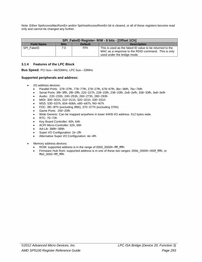
©2012 Advanced Micro Devices, Inc. LPC ISA Bridge (Device 20, Function 3) AMD SP5100 Register Reference Guide Page 293
Note: Either SpiAccessMacRomEn and/or SpiHostAccessRomEn bit is cleared, or all of these registers become read only and cannot be changed any further.
SPI_FakeID Register- R/W - 8 bits - [Offset 1Ch] Field Name Bits Default Description
SPI_FakeID 7:0 FFh This is used as the faked ID value to be returned to the MAC as a response to the RDID command. This is only used under the bridge mode.
3.1.4 Features of the LPC Block
Bus Speed: PCI bus—66/33MHz, LPC bus—33MHz Supported peripherals and address:
• I/O address devices: • Parallel Ports: 378~37fh, 778~77fh, 278~27fh, 678~67fh, 3bc~3bfh, 7bc~7bfh • Serial Ports: 3f8~3ffh, 2f8~2ffh, 220~227h, 228~22fh, 238~23fh, 2e8~2efh, 338~33fh, 3e8~3efh • Audio: 220~233h, 240~253h, 260~273h, 280~293h • MIDI: 300~301h, 310~311h, 320~321h, 330~331h • MSS: 530~537h, 604~60bh, e80~e87h, f40~f47h • FDC: 3f0~3f7h (excluding 3f6h), 370~377h (excluding 376h) • Game Ports: 200~20fh • Wide Generic: Can be mapped anywhere in lower 64KB I/O address. 512 bytes wide. • RTC: 70~73h • Key Board Controller: 60h, 64h • ACPI Micro-Controller: 62h, 66h • Ad-Lib: 388h~389h • Super I/O Configuration: 2e~2fh • Alternative Super I/O Configuration: 4e~4fh
• Memory address devices:
• ROM: supported address is in the range of 0000_0000h~ffff_ffffh • Firmware Hub Rom: supported address is in one of these two ranges: 000e_0000h~000f_ffffh, or
ffb0_0000~ffff_ffffh
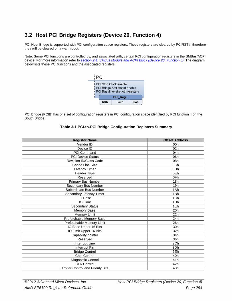
©2012 Advanced Micro Devices, Inc. Host PCI Bridge Registers (Device 20, Function 4) AMD SP5100 Register Reference Guide Page 294
3.2 Host PCI Bridge Registers (Device 20, Function 4) PCI Host Bridge is supported with PCI configuration space registers. These registers are cleared by PCIRST#; therefore they will be cleared on a warm boot. Note: Some PCI functions are controlled by, and associated with, certain PCI configuration registers in the SMBus/ACPI device. For more information refer to section 2.4: SMBus Module and ACPI Block (Device 20, Function 0). The diagram below lists these PCI functions and the associated registers.
PCI Bridge (PCIB) has one set of configuration registers in PCI configuration space identified by PCI function 4 on the South Bridge.
Table 3-1 PCI-to-PCI Bridge Configuration Registers Summary
Register Name Offset Address Vendor ID 00h Device ID 02h
PCI Command 04h PCI Device Status 06h
Revision ID/Class Code 08h Cache Line Size 0Ch Latency Timer 0Dh Header Type 0Eh
Reserved 0Fh Primary Bus Number 18h
Secondary Bus Number 19h Subordinate Bus Number 1Ah Secondary Latency Timer 1Bh
IO Base 1Ch IO Limit 1Dh
Secondary Status 1Eh Memory Base 20h Memory Limit 22h
Prefetchable Memory Base 24h Prefetchable Memory Limit 26h
IO Base Upper 16 Bits 30h IO Limit Upper 16 Bits 32h
Capability pointer 34h Reserved 36h
Interrupt Line 3Ch Interrupt Pin 3Dh
Bridge Control 3Eh Chip Control 40h
Diagnostic Control 41h CLK Control 42h
Arbiter Control and Priority Bits 43h
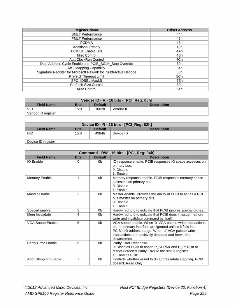
©2012 Advanced Micro Devices, Inc. Host PCI Bridge Registers (Device 20, Function 4) AMD SP5100 Register Reference Guide Page 295
Register Name Offset Address SMLT Performance 44h PMLT Performance 46h
PCDMA 48h Additional Priority 49h
PCICLK Enable Bits 4Ah Misc Control 4Bh
AutoClockRun Control 4Ch Dual Address Cycle Enable and PCIB_SCLK_Stop Override 50h
MSI Mapping Capability 54h Signature Register for Microsoft Rework for Subtractive Decode 58h
Prefetch Timeout Limit 5Ch SPCI IDSEL MaskB 5Eh
Prefetch Size Control 60h Misc Control 64h
Vender ID - R - 16 bits - [PCI_Reg: 00h] Field Name Bits Default Description
VID 15:0 1002h Vendor ID Vendor ID register
Device ID - R - 16 bits - [PCI_Reg: 02h] Field Name Bits Default Description
DID 15:0 4384h Device ID
Device ID register
Command - RW - 16 bits - [PCI_Reg: 04h] Field Name Bits Default Description
IO Enable 0 0b IO response enable. PCIB responses IO space accesses on primary bus. 0: Disable 1: Enable
Memory Enable 1 0b Memory response enable. PCIB responses memory space accesses on primary bus. 0: Disable 1: Enable
Master Enable 2 0b Master enable. Provides the ability of PCIB to act as a PCI bus master on primary bus. 0: Disable 1: Enable
Special Enable 3 0b Hardwired to 0 to indicate that PCIB ignores special cycles. Mem Invalidate 4 0b Hardwired to 0 to indicate that PCIB doesn’t issue memory
write and invalidate command by itself. VGA Snoop Enable 5 0b VGA snoop enable. When ‘0’ VGA palette write transactions
on the primary interface are ignored unless it falls into PCIB’s IO address range. When ‘1’ VGA palette write transactions are positively decoded and forwarded downstream.
Parity Error Enable 6 0b Parity Error Response. 0: Disables PCIB to assert P_SERR# and P_PERR# or report Detected Parity Error to the status register 1: Enables PCIB.
Addr Stepping Enable 7 0b Controls whether or not to do address/data stepping, PCIB doesn’t. Read Only
©2012 Advanced Micro Devices, Inc. Host PCI Bridge Registers (Device 20, Function 4) AMD SP5100 Register Reference Guide Page 296
Command - RW - 16 bits - [PCI_Reg: 04h] Field Name Bits Default Description
System Error Enable 8 0b SERR# enable. 0: Disables PCIB to assert P_SERR# and report Signaled System Error bit 1: Enables PCIB.
Fast Back-to-Back Enable
9 0b Hardwired to 0 to indicate that PCIB is not capable of issuing fast back-to-back transactions on the primary bus.
Reserved 15:10 00h Reserved PCI Command register
Status- RW - 16 bits - [PCI_Reg: 06h] Field Name Bits Default Description
Reserved 3:0 0h Reserved Capabilities List 4 0b Read only. This bit is 1 when Offset 40h [3] = 1. At other
time this bit is 0. 0: The bridge does not support the Capabilities List 1: The bridge supports the Capabilities List (Offset 34h is the pointer to the data structure).
66MHz Capable 5 1b Hardwired to 1 to indicate PCIB support of 66MHz primary interface.
Reserved 6 0b Reserved Fast Back-to-Back Capbable
7 1b Hardwired to 1 to indicate PCIB is capable of accepting fast back-to-back transactions on the primary bus.
Master Parity Error 8 0b Master Data Parity Error, assertion of P_PERR# (when PCIB acts as a master) is received, write clears it.
DevSel Timing 9:10 01b Hardwired to 01b to indicate PCIB will assert DEVSEL# with medium timing.
Target Abort 11 0b Signaled Target Abort, write clears it. Received Target Abort 12 0b Received Target Abort, write clears it. Received Master Abort 13 0b Received Master Abort, write clears it. Master Abort 14 0b Signaled System Error bit, write clears it. Parity Error 15 0b Detected Parity Error, PCIB detected a parity error and will
assert P_PERR#, write clears it. PCI device status register.
Revision ID/Class Code- R - 32 bits - [PCI_Reg: 08h] Field Name Bits Default Description
Revision ID 7:0 00h These bits are hardwired to 00h to indicate the revision level of the chip design (for the SP5100).
Class Code 31:8 060401h/ 060400h
A class code of 06h indicates a bridge device, a subclass code of 04h indicates PCI bridge and a programming interface of ‘01h’ indicates subtractive decoding on primary bus is supported. Based on Reg0x4B[7], this register is programmed as positive decode bridge or subtractive decode bridge.
Revision ID/Class Code register.
Cache Line Size- RW - 8 bits - [PCI_Reg: 0Ch] Field Name Bits Default Description
Cache Line Size 7:0 00h Read Only Cache line size register
Primary Master Latency Timer- RW - 8 bits - [PCI_Reg: 0Dh] Field Name Bits Default Description
Prim Latency Timer 7:0 00h Primary master latency timer. Sets the minimum time that the Primary bus master can retain the ownership of the bus.
©2012 Advanced Micro Devices, Inc. Host PCI Bridge Registers (Device 20, Function 4) AMD SP5100 Register Reference Guide Page 297
Primary Master Latency Timer- RW - 8 bits - [PCI_Reg: 0Dh] Field Name Bits Default Description
Primary Master Latency timer register
Header Type- R - 8 bits - [PCI_Reg: 0Eh] Field Name Bits Default Description
Header Type 7:0 81h Indicates the bridge is a multi-function device. Header type register
Primary Bus Number- RW - 8 bits - [PCI_Reg: 18h] Field Name Bits Default Description
Primary Bus Number 7:0 00h Bus number of the PCI bus to which the primary interface is connected.
Primary Bus Number register
Secondary Bus Number - RW - 8 bits - [PCI_Reg: 19h] Field Name Bits Default Description
Secondary Bus Number 7:0 00h Bus number of the PCI bus to which the secondary interface is connected.
Secondary Bus Number register
SUBBN- RW - 8 bits - [PCI_Reg: 1Ah] Field Name Bits Default Description
SubordinateBusNum 7:0 00h Bus number of the highest numbered PCI bus behind PCIB. Subordinate Bus Number register
Secondary Latency Timber- RW - 8 bits - [PCI_Reg: 1Bh] Field Name Bits Default Description
Secondary Latency Timer
7:0 00h Secondary Master latency control timer. Sets the minimum time that the Secondary bus master can retain the ownership of the bus.
Secondary Master Latency Timer register
IO Base- RW - 8 bits - [PCI_Reg: 1Ch] Field Name Bits Default Description
IO16 1:0 00b Indicates a 16-bit IO address space. Read Only Can be changed to 32-bit when bit[29] of regx48 is set
Reserved 3:2 00b Reserved IOBase 7:4 0h Defines the bits [15:12] of the base address of 16-bit or 32-
bit IO space. IO base register
IO Limit- RW - 16 bits - [PCI_Reg: 1Dh] Field Name Bits Default Description
IO16 1:0 00b Indicates a 16-bit IO address space. Read Only Can be changed to 32-bit when bit[29] of regx48 is set
Reserved 3:2 00b Reserved IO Limit 7:4 0h Defines bits [15:12] of the limit of 16-bit or 32-bit IO space. IO Limit register
Secondary Status- RW - 16 bits - [PCI_Reg: 1Eh] Field Name Bits Default Description
Reserved 4:0 00h Reserved
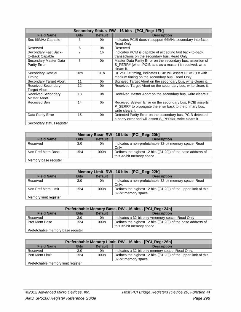
©2012 Advanced Micro Devices, Inc. Host PCI Bridge Registers (Device 20, Function 4) AMD SP5100 Register Reference Guide Page 298
Secondary Status- RW - 16 bits - [PCI_Reg: 1Eh] Field Name Bits Default Description
Sec 66MHz Capable 5 0b Indicates PCIB doesn’t support 66MHz secondary interface. Read Only.
Reserved 6 0b Reserved Secondary Fast Back-to-Back Capable
7 1b Indicates PCIB is capable of accepting fast back-to-back transactions on the secondary bus. Read Only.
Secondary Master Data Parity Error
8 0b Master Data Parity Error on the secondary bus, assertion of S_PERR# (when PCIB acts as a master) is received, write clears it.
Secondary DevSel Timing
10:9 01b DEVSEL# timing, indicates PCIB will assert DEVSEL# with medium timing on the secondary bus. Read Only.
Secondary Target Abort 11 0b Signaled Target Abort on the secondary bus, write clears it. Received Secondary Target Abort
12 0b Received Target Abort on the secondary bus, write clears it.
Received Secondary Master Abort
13 0b Received Master Abort on the secondary bus, write clears it.
Received Serr 14 0b Received System Error on the secondary bus, PCIB asserts P_SERR# to propagate the error back to the primary bus, write clears it.
Data Parity Error 15 0b Detected Parity Error on the secondary bus, PCIB detected a parity error and will assert S_PERR#, write clears it.
Secondary status register
Memory Base- RW - 16 bits - [PCI_Reg: 20h] Field Name Bits Default Description
Reserved 3:0 0h Indicates a non-prefetchable 32-bit memory space. Read Only
Non Pref Mem Base 15:4 000h Defines the highest 12 bits ([31:20]) of the base address of this 32-bit memory space.
Memory base register
Memory Limit- RW - 16 bits - [PCI_Reg: 22h] Field Name Bits Default Description
Reserved 3:0 0h Indicates a non-prefetchable 32-bit memory space. Read Only.
Non Pref Mem Limit 15:4 000h Defines the highest 12 bits ([31:20]) of the upper limit of this 32-bit memory space.
Memory limit register
Prefetchable Memory Base- RW - 16 bits - [PCI_Reg: 24h] Field Name Bits Default Description
Reserved 3:0 0h Indicates a 32-bit only +memory space. Read Only Pref Mem Base 15:4 000h Defines the highest 12 bits ([31:20]) of the base address of
this 32-bit memory space. Prefetchable memory base register
Prefetchable Memory Limit- RW - 16 bits - [PCI_Reg: 26h] Field Name Bits Default Description
Reserved 3:0 0h Indicates a 32-bit only memory space. Read Only. Perf Mem Limit 15:4 000h Defines the highest 12 bits ([31:20]) of the upper limit of this
32-bit memory space. Prefetchable memory limit register
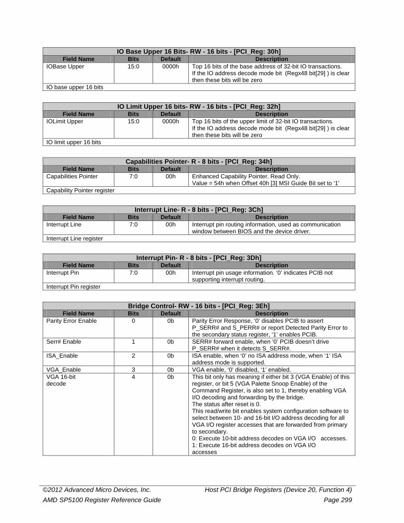
©2012 Advanced Micro Devices, Inc. Host PCI Bridge Registers (Device 20, Function 4) AMD SP5100 Register Reference Guide Page 299
IO Base Upper 16 Bits- RW - 16 bits - [PCI_Reg: 30h] Field Name Bits Default Description
IOBase Upper 15:0 0000h Top 16 bits of the base address of 32-bit IO transactions. If the IO address decode mode bit (Regx48 bit[29] ) is clear then these bits will be zero
IO base upper 16 bits
IO Limit Upper 16 bits- RW - 16 bits - [PCI_Reg: 32h] Field Name Bits Default Description
IOLimit Upper 15:0 0000h Top 16 bits of the upper limit of 32-bit IO transactions. If the IO address decode mode bit (Regx48 bit[29] ) is clear then these bits will be zero
IO limit upper 16 bits
Capabilities Pointer- R - 8 bits - [PCI_Reg: 34h] Field Name Bits Default Description
Capabilities Pointer 7:0 00h Enhanced Capability Pointer. Read Only. Value = 54h when Offset 40h [3] MSI Guide Bit set to ‘1’
Capability Pointer register
Interrupt Line- R - 8 bits - [PCI_Reg: 3Ch] Field Name Bits Default Description
Interrupt Line 7:0 00h Interrupt pin routing information, used as communication window between BIOS and the device driver.
Interrupt Line register
Interrupt Pin- R - 8 bits - [PCI_Reg: 3Dh] Field Name Bits Default Description
Interrupt Pin 7:0 00h Interrupt pin usage information. ‘0’ indicates PCIB not supporting interrupt routing.
Interrupt Pin register
Bridge Control- RW - 16 bits - [PCI_Reg: 3Eh] Field Name Bits Default Description
Parity Error Enable 0 0b Parity Error Response, ‘0’ disables PCIB to assert P_SERR# and S_PERR# or report Detected Parity Error to the secondary status register, ‘1’ enables PCIB.
Serr# Enable 1 0b SERR# forward enable, when ‘0’ PCIB doesn’t drive P_SERR# when it detects S_SERR#.
ISA_Enable 2 0b ISA enable, when ‘0’ no ISA address mode, when ‘1’ ISA address mode is supported.
VGA_Enable 3 0b VGA enable, ‘0’ disabled, ‘1’ enabled. VGA 16-bit decode
4 0b This bit only has meaning if either bit 3 (VGA Enable) of this register, or bit 5 (VGA Palette Snoop Enable) of the Command Register, is also set to 1, thereby enabling VGA I/O decoding and forwarding by the bridge. The status after reset is 0. This read/write bit enables system configuration software to select between 10- and 16-bit I/O address decoding for all VGA I/O register accesses that are forwarded from primary to secondary. 0: Execute 10-bit address decodes on VGA I/O accesses. 1: Execute 16-bit address decodes on VGA I/O accesses
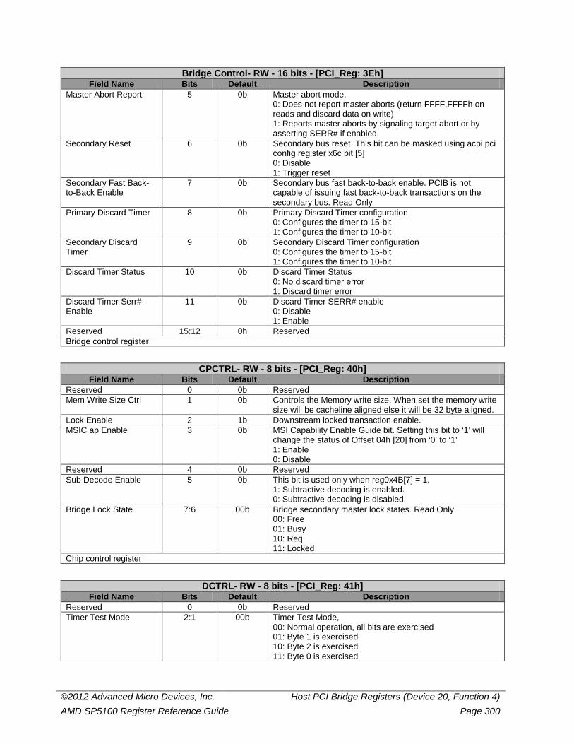
©2012 Advanced Micro Devices, Inc. Host PCI Bridge Registers (Device 20, Function 4) AMD SP5100 Register Reference Guide Page 300
Bridge Control- RW - 16 bits - [PCI_Reg: 3Eh] Field Name Bits Default Description
Master Abort Report 5 0b Master abort mode. 0: Does not report master aborts (return FFFF,FFFFh on reads and discard data on write) 1: Reports master aborts by signaling target abort or by asserting SERR# if enabled.
Secondary Reset 6 0b Secondary bus reset. This bit can be masked using acpi pci config register x6c bit [5] 0: Disable 1: Trigger reset
Secondary Fast Back-to-Back Enable
7 0b Secondary bus fast back-to-back enable. PCIB is not capable of issuing fast back-to-back transactions on the secondary bus. Read Only
Primary Discard Timer 8 0b Primary Discard Timer configuration 0: Configures the timer to 15-bit 1: Configures the timer to 10-bit
Secondary Discard Timer
9 0b Secondary Discard Timer configuration 0: Configures the timer to 15-bit 1: Configures the timer to 10-bit
Discard Timer Status 10 0b Discard Timer Status 0: No discard timer error 1: Discard timer error
Discard Timer Serr# Enable
11 0b Discard Timer SERR# enable 0: Disable 1: Enable
Reserved 15:12 0h Reserved Bridge control register
CPCTRL- RW - 8 bits - [PCI_Reg: 40h] Field Name Bits Default Description
Reserved 0 0b Reserved Mem Write Size Ctrl 1 0b Controls the Memory write size. When set the memory write
size will be cacheline aligned else it will be 32 byte aligned. Lock Enable 2 1b Downstream locked transaction enable. MSIC ap Enable 3 0b MSI Capability Enable Guide bit. Setting this bit to ‘1’ will
change the status of Offset 04h [20] from ‘0’ to ‘1’ 1: Enable 0: Disable
Reserved 4 0b Reserved Sub Decode Enable 5 0b This bit is used only when reg0x4B[7] = 1.
1: Subtractive decoding is enabled. 0: Subtractive decoding is disabled.
Bridge Lock State 7:6 00b Bridge secondary master lock states. Read Only 00: Free 01: Busy 10: Req 11: Locked
Chip control register
DCTRL- RW - 8 bits - [PCI_Reg: 41h] Field Name Bits Default Description
Reserved 0 0b Reserved Timer Test Mode 2:1 00b Timer Test Mode,
00: Normal operation, all bits are exercised 01: Byte 1 is exercised 10: Byte 2 is exercised 11: Byte 0 is exercised
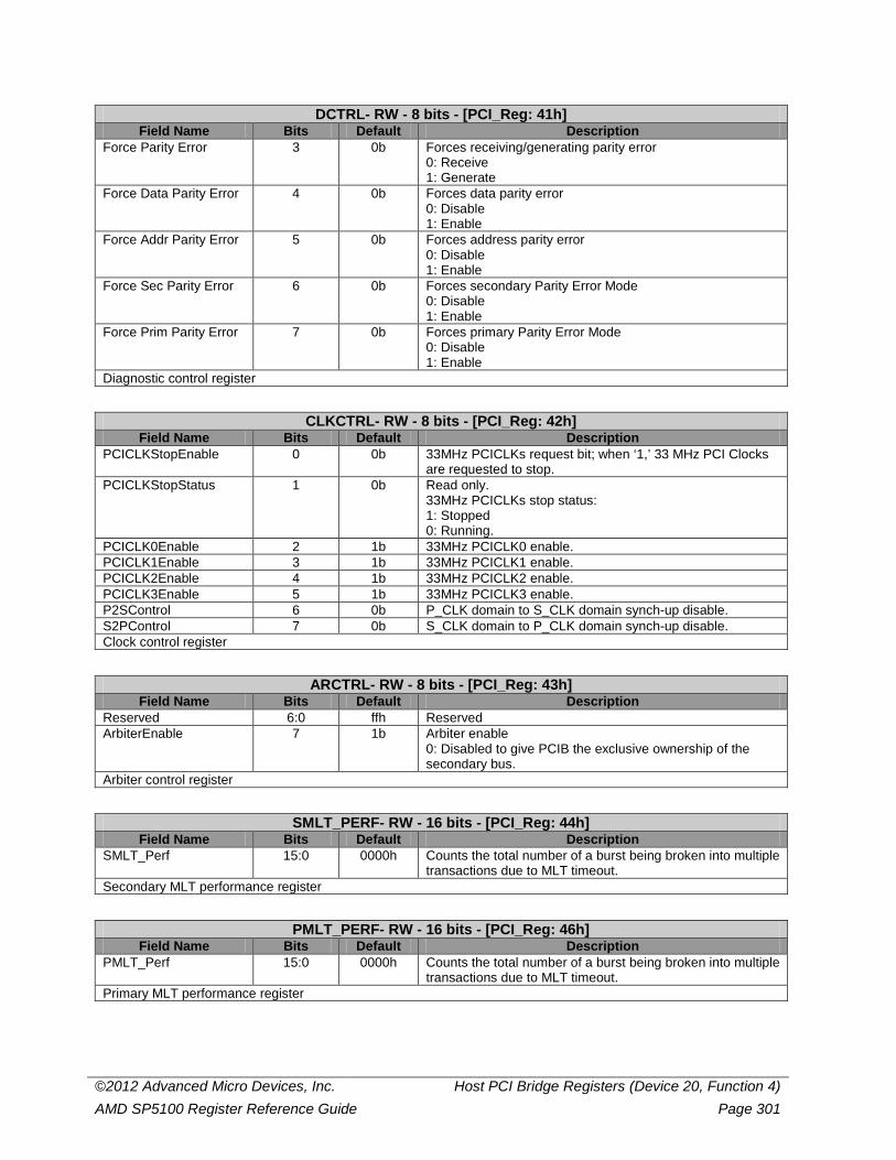
©2012 Advanced Micro Devices, Inc. Host PCI Bridge Registers (Device 20, Function 4) AMD SP5100 Register Reference Guide Page 301
DCTRL- RW - 8 bits - [PCI_Reg: 41h] Field Name Bits Default Description
Force Parity Error 3 0b Forces receiving/generating parity error 0: Receive 1: Generate
Force Data Parity Error 4 0b Forces data parity error 0: Disable 1: Enable
Force Addr Parity Error 5 0b Forces address parity error 0: Disable 1: Enable
Force Sec Parity Error 6 0b Forces secondary Parity Error Mode 0: Disable 1: Enable
Force Prim Parity Error 7 0b Forces primary Parity Error Mode 0: Disable 1: Enable
Diagnostic control register
CLKCTRL- RW - 8 bits - [PCI_Reg: 42h] Field Name Bits Default Description
PCICLKStopEnable 0 0b 33MHz PCICLKs request bit; when ‘1,’ 33 MHz PCI Clocks are requested to stop.
PCICLKStopStatus 1 0b Read only. 33MHz PCICLKs stop status: 1: Stopped 0: Running.
PCICLK0Enable 2 1b 33MHz PCICLK0 enable. PCICLK1Enable 3 1b 33MHz PCICLK1 enable. PCICLK2Enable 4 1b 33MHz PCICLK2 enable. PCICLK3Enable 5 1b 33MHz PCICLK3 enable. P2SControl 6 0b P_CLK domain to S_CLK domain synch-up disable. S2PControl 7 0b S_CLK domain to P_CLK domain synch-up disable. Clock control register
ARCTRL- RW - 8 bits - [PCI_Reg: 43h] Field Name Bits Default Description
Reserved 6:0 ffh Reserved ArbiterEnable 7 1b Arbiter enable
0: Disabled to give PCIB the exclusive ownership of the secondary bus.
Arbiter control register
SMLT_PERF- RW - 16 bits - [PCI_Reg: 44h] Field Name Bits Default Description
SMLT_Perf 15:0 0000h Counts the total number of a burst being broken into multiple transactions due to MLT timeout.
Secondary MLT performance register
PMLT_PERF- RW - 16 bits - [PCI_Reg: 46h] Field Name Bits Default Description
PMLT_Perf 15:0 0000h Counts the total number of a burst being broken into multiple transactions due to MLT timeout.
Primary MLT performance register
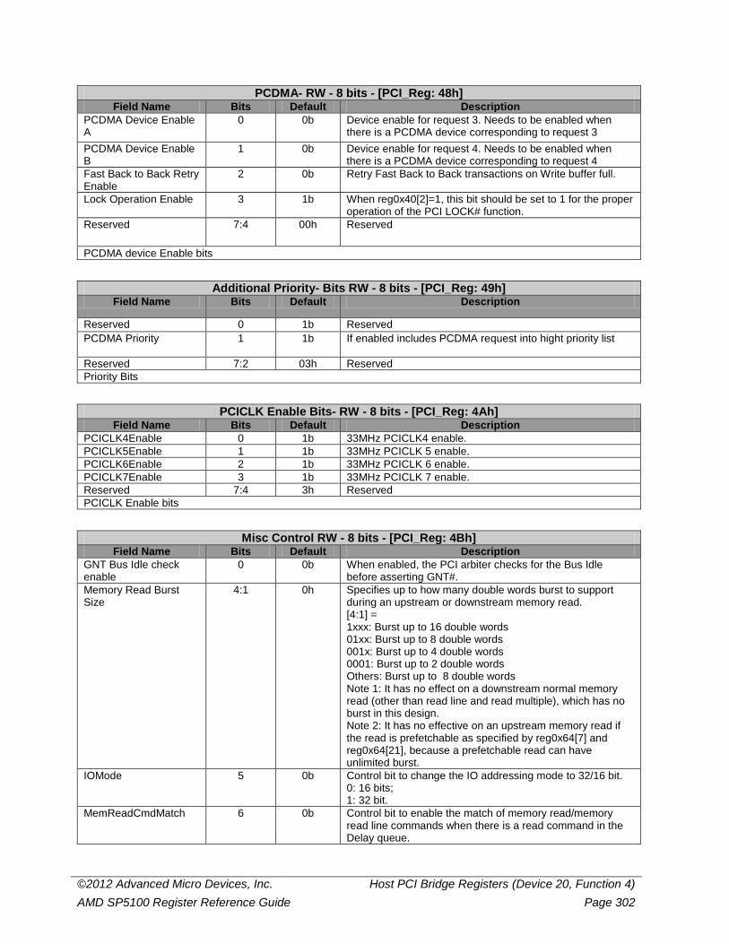
©2012 Advanced Micro Devices, Inc. Host PCI Bridge Registers (Device 20, Function 4) AMD SP5100 Register Reference Guide Page 302
PCDMA- RW - 8 bits - [PCI_Reg: 48h] Field Name Bits Default Description
PCDMA Device Enable A
0 0b Device enable for request 3. Needs to be enabled when there is a PCDMA device corresponding to request 3
PCDMA Device Enable B
1 0b Device enable for request 4. Needs to be enabled when there is a PCDMA device corresponding to request 4
Fast Back to Back Retry Enable
2 0b Retry Fast Back to Back transactions on Write buffer full.
Lock Operation Enable 3 1b When reg0x40[2]=1, this bit should be set to 1 for the proper operation of the PCI LOCK# function.
Reserved 7:4 00h Reserved
PCDMA device Enable bits
Additional Priority- Bits RW - 8 bits - [PCI_Reg: 49h] Field Name Bits Default Description
Reserved 0 1b Reserved PCDMA Priority 1 1b If enabled includes PCDMA request into hight priority list
Reserved 7:2 03h Reserved Priority Bits
PCICLK Enable Bits- RW - 8 bits - [PCI_Reg: 4Ah] Field Name Bits Default Description
PCICLK4Enable 0 1b 33MHz PCICLK4 enable. PCICLK5Enable 1 1b 33MHz PCICLK 5 enable. PCICLK6Enable 2 1b 33MHz PCICLK 6 enable. PCICLK7Enable 3 1b 33MHz PCICLK 7 enable. Reserved 7:4 3h Reserved PCICLK Enable bits
Misc Control RW - 8 bits - [PCI_Reg: 4Bh] Field Name Bits Default Description
GNT Bus Idle check enable
0 0b When enabled, the PCI arbiter checks for the Bus Idle before asserting GNT#.
Memory Read Burst Size
4:1 0h Specifies up to how many double words burst to support during an upstream or downstream memory read. [4:1] = 1xxx: Burst up to 16 double words 01xx: Burst up to 8 double words 001x: Burst up to 4 double words 0001: Burst up to 2 double words Others: Burst up to 8 double words Note 1: It has no effect on a downstream normal memory read (other than read line and read multiple), which has no burst in this design. Note 2: It has no effective on an upstream memory read if the read is prefetchable as specified by reg0x64[7] and reg0x64[21], because a prefetchable read can have unlimited burst.
IOMode 5 0b Control bit to change the IO addressing mode to 32/16 bit. 0: 16 bits; 1: 32 bit.
MemReadCmdMatch 6 0b Control bit to enable the match of memory read/memory read line commands when there is a read command in the Delay queue.
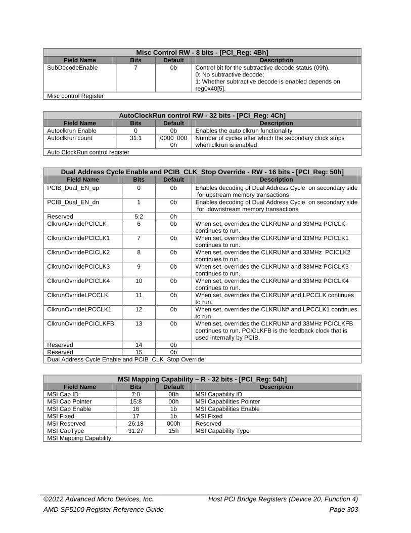
©2012 Advanced Micro Devices, Inc. Host PCI Bridge Registers (Device 20, Function 4) AMD SP5100 Register Reference Guide Page 303
Misc Control RW - 8 bits - [PCI_Reg: 4Bh] Field Name Bits Default Description
SubDecodeEnable 7 0b Control bit for the subtractive decode status (09h). 0: No subtractive decode; 1: Whether subtractive decode is enabled depends on reg0x40[5].
Misc control Register
AutoClockRun control RW - 32 bits - [PCI_Reg: 4Ch] Field Name Bits Default Description
Autoclkrun Enable 0 0b Enables the auto clkrun functionality Autoclkrun count 31:1 0000_000
0h Number of cycles after which the secondary clock stops when clkrun is enabled
Auto ClockRun control register
Dual Address Cycle Enable and PCIB_CLK_Stop Override - RW - 16 bits - [PCI_Reg: 50h] Field Name Bits Default Description
PCIB_Dual_EN_up 0 0b Enables decoding of Dual Address Cycle on secondary side for upstream memory transactions
PCIB_Dual_EN_dn 1 0b Enables decoding of Dual Address Cycle on secondary side for downstream memory transactions
Reserved 5:2 0h ClkrunOvrridePCICLK 6 0b When set, overrides the CLKRUN# and 33MHz PCICLK
continues to run. ClkrunOvrridePCICLK1 7 0b When set, overrides the CLKRUN# and 33MHz PCICLK1
continues to run. ClkrunOvrridePCICLK2 8 0b When set, overrides the CLKRUN# and 33MHz PCICLK2
continues to run. ClkrunOvrridePCICLK3 9 0b When set, overrides the CLKRUN# and 33MHz PCICLK3
continues to run. ClkrunOvrridePCICLK4 10 0b When set, overrides the CLKRUN# and 33MHz PCICLK4
continues to run. ClkrunOvrrideLPCCLK 11 0b When set, overrides the CLKRUN# and LPCCLK continues
to run. ClkrunOvrrideLPCCLK1 12 0b When set, overrides the CLKRUN# and LPCCLK1 continues
to run ClkrunOvrridePCICLKFB 13 0b When set, overrides the CLKRUN# and 33MHz PCICLKFB
continues to run. PCICLKFB is the feedback clock that is used internally by PCIB.
Reserved 14 0b Reserved 15 0b Dual Address Cycle Enable and PCIB_CLK_Stop Override
MSI Mapping Capability – R - 32 bits - [PCI_Reg: 54h] Field Name Bits Default Description
MSI Cap ID 7:0 08h MSI Capability ID MSI Cap Pointer 15:8 00h MSI Capabilities Pointer MSI Cap Enable 16 1b MSI Capabilities Enable MSI Fixed 17 1b MSI Fixed MSI Reserved 26:18 000h Reserved MSI CapType 31:27 15h MSI Capability Type MSI Mapping Capability

©2012 Advanced Micro Devices, Inc. Host PCI Bridge Registers (Device 20, Function 4) AMD SP5100 Register Reference Guide Page 304
Signature Register for Microsoft Rework for Subtractive Decode - R - 32 bits - [PCI_Reg: 58h]
Field Name Bits Default Description Signature Register for Microsoft Rework for Subtractive Decode
31:0 00000000h
When Microsoft Rework for Subtractive Decode is done, this register will contain the signature value
Signature Register for Microsoft Rework for Subtractive Decode
Prefetch Timeout Limit - 16 bits - [PCI_Reg: 5Ch] Field Name Bits Default Description
Prefetch Timeout Limit 15:0 0085h When deep prefetch is enabled (reg0x64[7]=1), this timer determines when to flush the staled data in the buffer. Each count is 30ns
SPCI IDSEL MaskB - 16 bits - [PCI_Reg: 5Eh] Field Name Bits Default Description
PCI IDSEL MaskB 15:0 FFFFh Each bit represents the masking the specific device on the PCI bus. The purpose of this register is to hide the device from OS 0: The corresponding IDSEL bit is masked 1: The corresponding IDSEL bit is not masked.
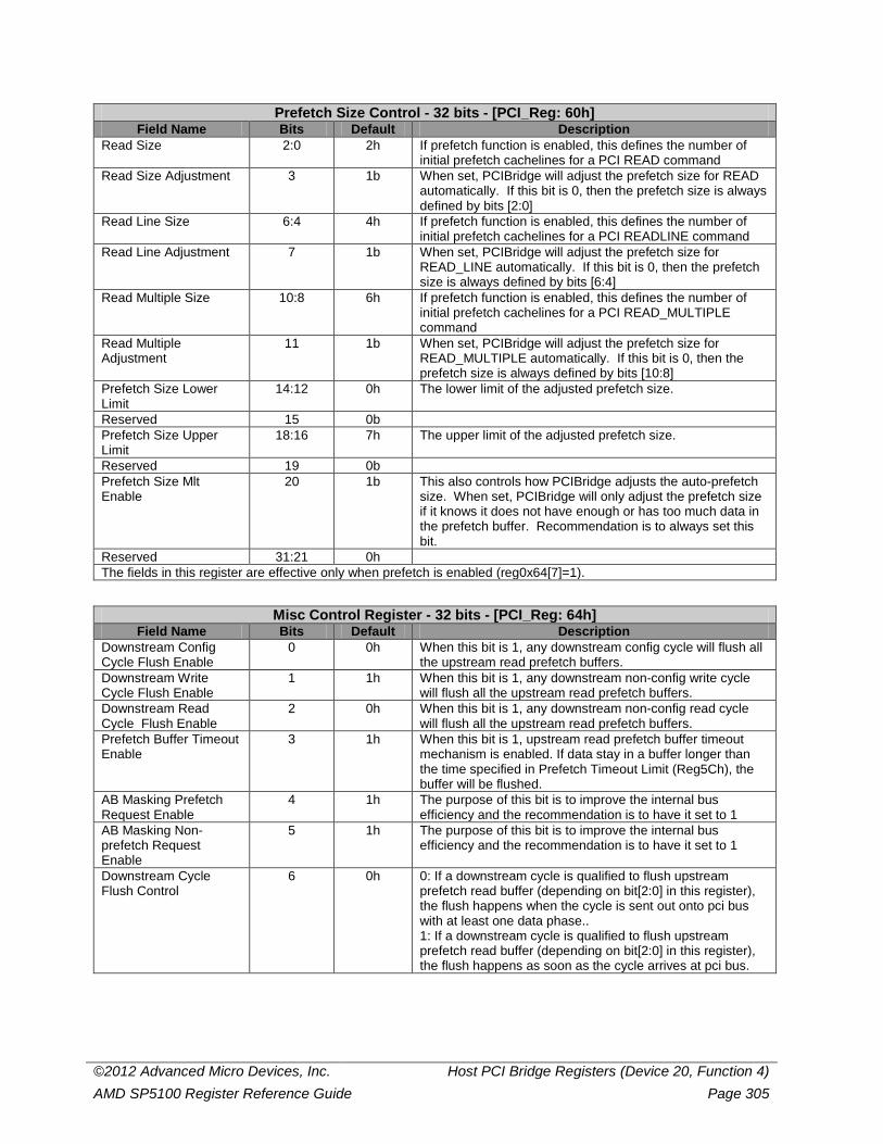
©2012 Advanced Micro Devices, Inc. Host PCI Bridge Registers (Device 20, Function 4) AMD SP5100 Register Reference Guide Page 305
Prefetch Size Control - 32 bits - [PCI_Reg: 60h] Field Name Bits Default Description
Read Size 2:0 2h If prefetch function is enabled, this defines the number of initial prefetch cachelines for a PCI READ command
Read Size Adjustment 3 1b When set, PCIBridge will adjust the prefetch size for READ automatically. If this bit is 0, then the prefetch size is always defined by bits [2:0]
Read Line Size 6:4 4h If prefetch function is enabled, this defines the number of initial prefetch cachelines for a PCI READLINE command
Read Line Adjustment 7 1b When set, PCIBridge will adjust the prefetch size for READ_LINE automatically. If this bit is 0, then the prefetch size is always defined by bits [6:4]
Read Multiple Size 10:8 6h If prefetch function is enabled, this defines the number of initial prefetch cachelines for a PCI READ_MULTIPLE command
Read Multiple Adjustment
11 1b When set, PCIBridge will adjust the prefetch size for READ_MULTIPLE automatically. If this bit is 0, then the prefetch size is always defined by bits [10:8]
Prefetch Size Lower Limit
14:12 0h The lower limit of the adjusted prefetch size.
Reserved 15 0b Prefetch Size Upper Limit
18:16 7h The upper limit of the adjusted prefetch size.
Reserved 19 0b Prefetch Size Mlt Enable
20 1b This also controls how PCIBridge adjusts the auto-prefetch size. When set, PCIBridge will only adjust the prefetch size if it knows it does not have enough or has too much data in the prefetch buffer. Recommendation is to always set this bit.
Reserved 31:21 0h The fields in this register are effective only when prefetch is enabled (reg0x64[7]=1).
Misc Control Register - 32 bits - [PCI_Reg: 64h] Field Name Bits Default Description
Downstream Config Cycle Flush Enable
0 0h When this bit is 1, any downstream config cycle will flush all the upstream read prefetch buffers.
Downstream Write Cycle Flush Enable
1 1h When this bit is 1, any downstream non-config write cycle will flush all the upstream read prefetch buffers.
Downstream Read Cycle Flush Enable
2 0h When this bit is 1, any downstream non-config read cycle will flush all the upstream read prefetch buffers.
Prefetch Buffer Timeout Enable
3 1h When this bit is 1, upstream read prefetch buffer timeout mechanism is enabled. If data stay in a buffer longer than the time specified in Prefetch Timeout Limit (Reg5Ch), the buffer will be flushed.
AB Masking Prefetch Request Enable
4 1h The purpose of this bit is to improve the internal bus efficiency and the recommendation is to have it set to 1
AB Masking Non-prefetch Request Enable
5 1h The purpose of this bit is to improve the internal bus efficiency and the recommendation is to have it set to 1
Downstream Cycle Flush Control
6 0h 0: If a downstream cycle is qualified to flush upstream prefetch read buffer (depending on bit[2:0] in this register), the flush happens when the cycle is sent out onto pci bus with at least one data phase.. 1: If a downstream cycle is qualified to flush upstream prefetch read buffer (depending on bit[2:0] in this register), the flush happens as soon as the cycle arrives at pci bus.
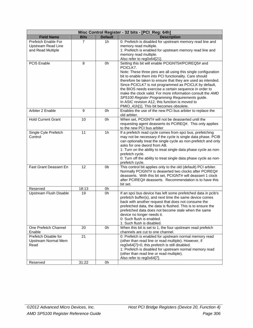
©2012 Advanced Micro Devices, Inc. Host PCI Bridge Registers (Device 20, Function 4) AMD SP5100 Register Reference Guide Page 306
Misc Control Register - 32 bits - [PCI_Reg: 64h] Field Name Bits Default Description
Prefetch Enable For Upstream Read Line and Read Multiple
7 1h 0: Prefetch is disabled for upstream memory read line and memory read multiple. 1: Prefetch is enabled for upstream memory read line and memory read multiple. Also refer to reg0x64[21].
PCI5 Enable 8 0h Setting this bit will enable PCIGNT5#/PCIREQ5# and PCICLK7. Note: These three pins are all using this single configuration bit to enable them into PCI functionality. Care should therefore be taken to ensure that they are used as intended. Since PCICLK7 is not programmed as PCICLK by default, the BIOS needs exercise a certain sequence in order to make the clock valid. For more information consult the AMD SP5100 Register Programming Requirements guide. In ASIC revision A12, this function is moved to PMIO_41h[1]. This bit becomes obsolete.
Arbiter 2 Enable 9 0h Enables the use of the new PCI bus arbiter to replace the old arbiter.
Hold Current Grant 10 0h When set, PCIGNT# will not be deasserted until the requesting agent deasserts its PCIREQ#. This only applies to the new PCI bus arbiter
Single Cyle Prefetch Control
11 1h If a prefetch read cycle comes from spci bus, prefetching may not be necessary if the cycle is single data phase. PCIB can optionally treat the single cycle as non-prefetch and only asks for one dword from AB. 1: Turn on the ability to treat single data phase cycle as non-prefetch cycle. 0: Turn off the ability to treat single data phase cycle as non-prefetch cycle.
Fast Grant Deassert En 12 0b This control bit applies only to the old (default) PCI arbiter. Normally PCIGNT# is deaserted two clocks after PCIREQ# deasserts. With this bit set, PCIGNT# will deassert 1 clock after PCIREQ# deasserts. Recommendation is to have this bit set.
Reserved 18:13 0h Upstream Flush Disable 19 0h If an spci bus device has left some prefetched data in pcib's
prefetch buffer(s), and next time the same device comes back with another request that does not consume the prefetched data, the data is flushed. This is to ensure the prefetched data does not become stale when the same device no longer needs it. 0: Such flush is enabled. 1: Such flush is disabled.
One Prefetch Channel Enable
20 0h When this bit is set to 1, the four upstream read prefetch channels are cut to one channel.
Prefetch Disable for Upstream Normal Mem Read
21 0: Prefetch is enabled for upstream normal memory read (other than read line or read multiple). However, if reg0x64[7]=0, this prefetch is still disabled. 1: Prefetch is disabled for upstream normal memory read (other than read line or read multiple). Also refer to reg0x64[7].
Reserved 31:22 0h
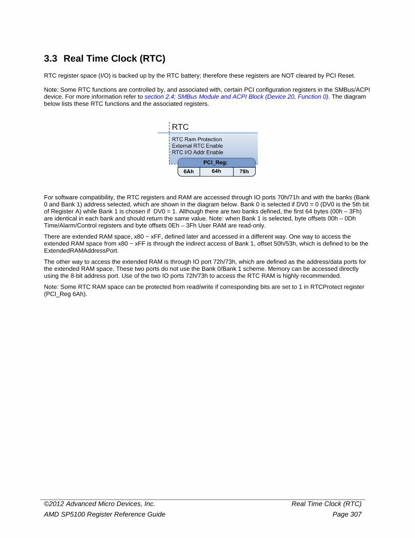
©2012 Advanced Micro Devices, Inc. Real Time Clock (RTC) AMD SP5100 Register Reference Guide Page 307
3.3 Real Time Clock (RTC) RTC register space (I/O) is backed up by the RTC battery; therefore these registers are NOT cleared by PCI Reset. Note: Some RTC functions are controlled by, and associated with, certain PCI configuration registers in the SMBus/ACPI device. For more information refer to section 2.4: SMBus Module and ACPI Block (Device 20, Function 0). The diagram below lists these RTC functions and the associated registers.
For software compatibility, the RTC registers and RAM are accessed through IO ports 70h/71h and with the banks (Bank 0 and Bank 1) address selected, which are shown in the diagram below. Bank 0 is selected if DV0 = 0 (DV0 is the 5th bit of Register A) while Bank 1 is chosen if DV0 = 1. Although there are two banks defined, the first 64 bytes (00h – 3Fh) are identical in each bank and should return the same value. Note: when Bank 1 is selected, byte offsets 00h – 0Dh Time/Alarm/Control registers and byte offsets 0Eh – 3Fh User RAM are read-only.
There are extended RAM space, x80 ~ xFF, defined later and accessed in a different way. One way to access the extended RAM space from x80 ~ xFF is through the indirect access of Bank 1, offset 50h/53h, which is defined to be the ExtendedRAMAddressPort.
The other way to access the extended RAM is through IO port 72h/73h, which are defined as the address/data ports for the extended RAM space. These two ports do not use the Bank 0/Bank 1 scheme. Memory can be accessed directly using the 8-bit address port. Use of the two IO ports 72h/73h to access the RTC RAM is highly recommended.
Note: Some RTC RAM space can be protected from read/write if corresponding bits are set to 1 in RTCProtect register (PCI_Reg 6Ah).
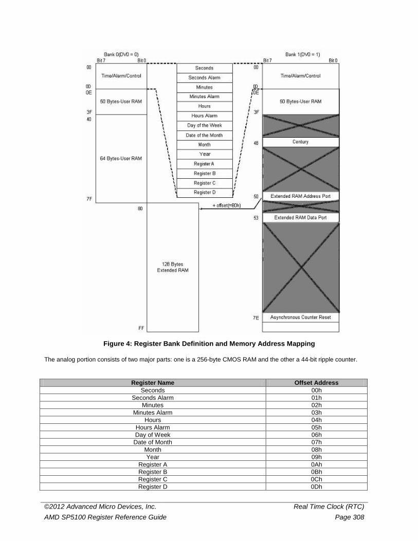
©2012 Advanced Micro Devices, Inc. Real Time Clock (RTC) AMD SP5100 Register Reference Guide Page 308
Figure 4: Register Bank Definition and Memory Address Mapping
The analog portion consists of two major parts: one is a 256-byte CMOS RAM and the other a 44-bit ripple counter.
Register Name Offset Address Seconds 00h
Seconds Alarm 01h Minutes 02h
Minutes Alarm 03h Hours 04h
Hours Alarm 05h Day of Week 06h
Date of Month 07h Month 08h Year 09h
Register A 0Ah Register B 0Bh Register C 0Ch Register D 0Dh

©2012 Advanced Micro Devices, Inc. Real Time Clock (RTC) AMD SP5100 Register Reference Guide Page 309
Register Name Offset Address AltCentury (when DV0=0) 32h
Century (when DV0=1) 48h Extended RAM Address Port 50h
Extended RAM Data Port 53h RTC Time Clear 7Eh
RTC RAM Enable 7Fh
Note: Registers that are implemented in the internal RTC are described below.
Seconds - RW – 8 bits - [RTC_Reg: 00h] Field Name Bits Default Description
Seconds 7:0 00h Binary-Code-Decimal format. Range:00 – 59 This register can be set by software (set bit of Register B = 1) or can be automatically updated by hardware every second. When set by software, hardware updating is disabled.
Seconds register
Seconds Alarm - RW – 8 bits - [RTC_Reg: 01h] Field Name Bits Default Description
Seconds Alarm 7:0 00h Binary-Code-Decimal format. If set bit = 1, the Seconds Alarm Register will never match with Seconds Register, else If bits [7:6] = [11], the Seconds Alarm Register always matches with Seconds Register.
Seconds Alarm register
Minutes - RW – 8 bits - [RTC_Reg: 02h] Field Name Bits Default Description
Minutes 7:0 00h Binary-Code-Decimal format. Range:00 – 59 This register can be set by software (set bit of Register B = 1) or can be automatically updated by hardware every minute. When set by software, hardware updating is disabled.
Minutes register
Minutes Alarm - RW – 8 bits - [RTC_Reg: 03h] Field Name Bits Default Description
Minutes Alarm 7:0 00h Binary-Code-Decimal format. If set bit = 1, the Minutes Alarm Register will never match with Minutes Register, else If bits [7:6] = [11], the Minutes Alarm Register always matches with Minutes Register.
Minutes Alarm register
Hours - RW – 8 bits - [RTC_Reg: 04h] Field Name Bits Default Description
Hours 7:0 00h Binary-Code-Decimal format. Range:00 – 23 This register can be set by software (set bit of Register B = 1) or can be automatically updated by hardware every hour. When set by software, hardware updating is disabled.
Hours register
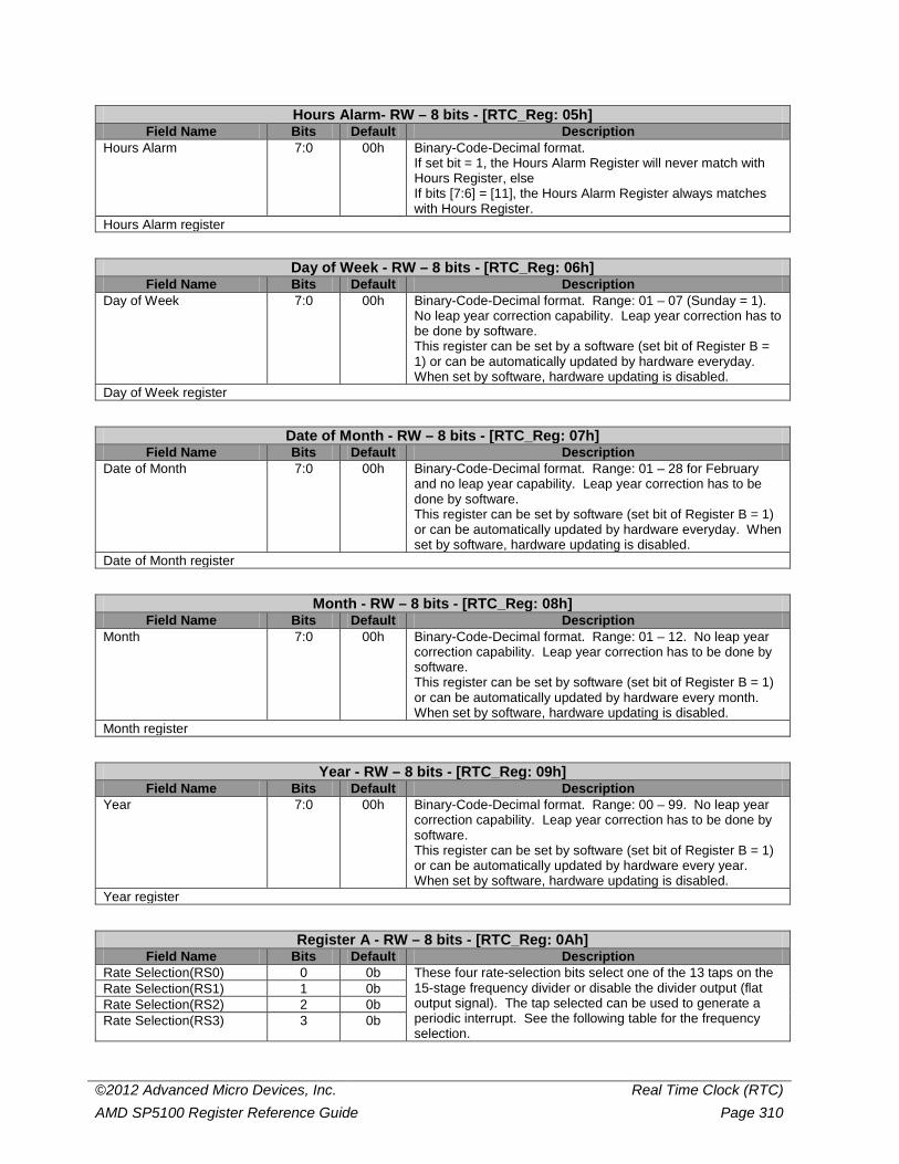
©2012 Advanced Micro Devices, Inc. Real Time Clock (RTC) AMD SP5100 Register Reference Guide Page 310
Hours Alarm- RW – 8 bits - [RTC_Reg: 05h] Field Name Bits Default Description
Hours Alarm 7:0 00h Binary-Code-Decimal format. If set bit = 1, the Hours Alarm Register will never match with Hours Register, else If bits [7:6] = [11], the Hours Alarm Register always matches with Hours Register.
Hours Alarm register
Day of Week - RW – 8 bits - [RTC_Reg: 06h] Field Name Bits Default Description
Day of Week 7:0 00h Binary-Code-Decimal format. Range: 01 – 07 (Sunday = 1). No leap year correction capability. Leap year correction has to be done by software. This register can be set by a software (set bit of Register B = 1) or can be automatically updated by hardware everyday. When set by software, hardware updating is disabled.
Day of Week register
Date of Month - RW – 8 bits - [RTC_Reg: 07h] Field Name Bits Default Description
Date of Month 7:0 00h Binary-Code-Decimal format. Range: 01 – 28 for February and no leap year capability. Leap year correction has to be done by software. This register can be set by software (set bit of Register B = 1) or can be automatically updated by hardware everyday. When set by software, hardware updating is disabled.
Date of Month register
Month - RW – 8 bits - [RTC_Reg: 08h] Field Name Bits Default Description
Month 7:0 00h Binary-Code-Decimal format. Range: 01 – 12. No leap year correction capability. Leap year correction has to be done by software. This register can be set by software (set bit of Register B = 1) or can be automatically updated by hardware every month. When set by software, hardware updating is disabled.
Month register
Year - RW – 8 bits - [RTC_Reg: 09h] Field Name Bits Default Description
Year 7:0 00h Binary-Code-Decimal format. Range: 00 – 99. No leap year correction capability. Leap year correction has to be done by software. This register can be set by software (set bit of Register B = 1) or can be automatically updated by hardware every year. When set by software, hardware updating is disabled.
Year register
Register A - RW – 8 bits - [RTC_Reg: 0Ah] Field Name Bits Default Description
Rate Selection(RS0) 0 0b These four rate-selection bits select one of the 13 taps on the 15-stage frequency divider or disable the divider output (flat output signal). The tap selected can be used to generate a periodic interrupt. See the following table for the frequency selection.
Rate Selection(RS1) 1 0b Rate Selection(RS2) 2 0b Rate Selection(RS3) 3 0b
©2012 Advanced Micro Devices, Inc. Real Time Clock (RTC) AMD SP5100 Register Reference Guide Page 311
Register A - RW – 8 bits - [RTC_Reg: 0Ah] Field Name Bits Default Description
Bank Selection(DV0) 4 0b DV0 = 0 selects Bank 0; DV0 = 1 selects Bank 1. The SP5100, it has an alternate way to access the RAM without the use of bank select bit. Port 72/73 can be used as the index to access the full 256 bytes of RAM directly.
Reserved 6:5 Update In Progress(UIP) See Note.
7 0b If set bit = 1, UIP is cleared. If UIP = 1, the update transfer will soon occur. If UIP = 0, the update transfer will not occur for at least 244us. [Read-only]
Register A: Control register Note: SP5100 A12 :The UIP high pulse is 270 µS Typical when SS on SRC clock is OFF and 100µ min when SRC SS is ON.
Rate Selection Bits Tap Frequency(Interrupt Rate) RS3 RS2 RS1 RS0 0 0 0 0 Flat Signal(None) 0 0 0 1 256 Hz (3.90625 ms) 0 0 1 0 128 Hz (7.8125 ms) 0 0 1 1 8.192 kHz (122.070 us) 0 1 0 0 4.096 kHz (244.141 us) 0 1 0 1 2.048 kHz (488.281 us) 0 1 1 0 1.024 kHz (976.5625 us) 0 1 1 1 512 Hz (1.953125 ms) 1 0 0 0 256 Hz (3.90625 ms) 1 0 0 1 128 Hz (7.8125 ms) 1 0 1 0 64 Hz (15.625 ms) 1 0 1 1 32 Hz (31.25 ms) 1 1 0 0 16 Hz (62.5 ms) 1 1 0 1 8 Hz (125 ms) 1 1 1 0 4 Hz (250 ms) 1 1 1 1 2 Hz (500 ms)
Register B - RW – 8 bits - [RTC_Reg: 0Bh] Field Name Bits Default Description
Daylight Saving Enable 0 0b Both this bit and RtcExt_Reg: 00h bit[0] need to be set to 1 to enable RTC daylight saving feature.
HourMode 1 0b Hour mode 0: 12 hour mode 1: 24 hour mode
Reserved 3:2 00 Update Ended Interrupt Enable(UIE) 4 0b UIE enables the Update End Flag (UF) bit in
Register C to assert IRQ. If set bit = 1, UIE is cleared.
Alarm Interrupt Enable (AIE) 5 0b AIE enables the Alarm Flag (AF) bit in Register C to assert IRQ.
Periodic Interrupt Enable (PIE) 6 0b PIE enables the Periodic Interrupt Flag (PF) bit in Register C to assert IRQ.
Set new time (SET) 7 0b If set bit = 1, no internal updating for Time Registers is allowed. If set bit = 0, the Time Registers are updated every second.
Register B: Control register

©2012 Advanced Micro Devices, Inc. Real Time Clock (RTC) AMD SP5100 Register Reference Guide Page 312
Register C - R – 8 bits - [RTC_Reg: 0Ch] Field Name Bits Default Description
Reserved 3:0 0h Update Ended Interrupt Flag(UF) 4 0b This bit is set to one after each update cycle.
Reading Register C clears UF. Alarm Interrupt Flag (AF) 5 0b This bit is set to one if second, minute and hour time
has matched the second, minute and hour alarm time. Reading Register C clears AF bit.
Periodic Interrupt Flag (PF) 6 0b This bit is set to one when an edge is detected on the selected tap (through RS3 to RS0) of the frequency divider. Reading Register C clears PF bit.
Interrupt Request Flag (IRQF) 7 0b Logically, IRQF = (PF*PIE)+(AF*AIE)+(UF*UIE)+(WF*WIE) where WF and WIE are defined in Extended Control Register 4A and 4B. Reading Register C clears IRQF bit. Any time the IRQF bit is set to one, the #IRQ pin is driven low.
Register C: Control register
DateAlarm - RW – 8 bits - [RTC_Reg: 0Dh] Field Name Bits Default Description
DateAlarm 5:0 00h DateAlarm in BCD format and is considered when it is set to non-zero value. If this value is set to 0, then date is not compared for alarm generation.
Scratchbit 6 0b VRT 7 1b Valid RAM and Time; refer to VRT_T1 and VRT_T2
registers (PMIO 3E/3F) Date Alarm Register
AltCentury - RW – 8 bits - [RTC_Reg: 32h] Field Name Bits Default Description
AltCentury 7:0 00h (This register is accessed only when DV0=0 and PM_Reg 7Ch Bit4=1.) Binary-Code-Decimal format. Leap year correction is done through hardware. This register can be set by software (set bit of Register B = 1) or can be automatically updated by hardware every century. When set by software, hardware updating is disabled.
AltCentury Register
Century - RW – 8 bits - [RTC_Reg: 48h] Field Name Bits Default Description
Century 7:0 00h (This register is accessed only when DV0=1) Binary-Code-Decimal format. Leap year correction is done through hardware. This register can be set by software (set bit of Register B = 1) or can be automatically updated by hardware every century. When set by software, hardware updating is disabled.
Century Register
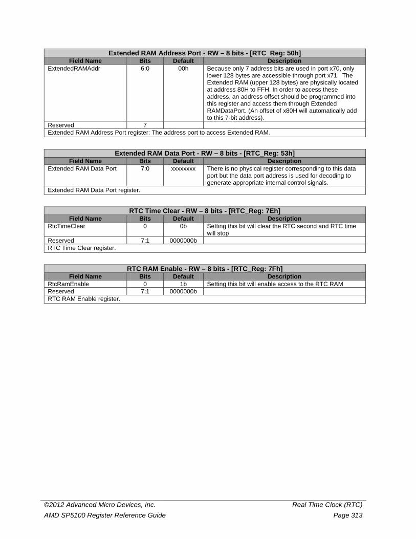
©2012 Advanced Micro Devices, Inc. Real Time Clock (RTC) AMD SP5100 Register Reference Guide Page 313
Extended RAM Address Port - RW – 8 bits - [RTC_Reg: 50h] Field Name Bits Default Description
ExtendedRAMAddr 6:0 00h Because only 7 address bits are used in port x70, only lower 128 bytes are accessible through port x71. The Extended RAM (upper 128 bytes) are physically located at address 80H to FFH. In order to access these address, an address offset should be programmed into this register and access them through Extended RAMDataPort. (An offset of x80H will automatically add to this 7-bit address).
Reserved 7 Extended RAM Address Port register: The address port to access Extended RAM.
Extended RAM Data Port - RW – 8 bits - [RTC_Reg: 53h] Field Name Bits Default Description
Extended RAM Data Port 7:0 xxxxxxxx There is no physical register corresponding to this data port but the data port address is used for decoding to generate appropriate internal control signals.
Extended RAM Data Port register.
RTC Time Clear - RW – 8 bits - [RTC_Reg: 7Eh] Field Name Bits Default Description
RtcTimeClear 0 0b Setting this bit will clear the RTC second and RTC time will stop
Reserved 7:1 0000000b RTC Time Clear register.
RTC RAM Enable - RW – 8 bits - [RTC_Reg: 7Fh] Field Name Bits Default Description
RtcRamEnable 0 1b Setting this bit will enable access to the RTC RAM Reserved 7:1 0000000b RTC RAM Enable register.
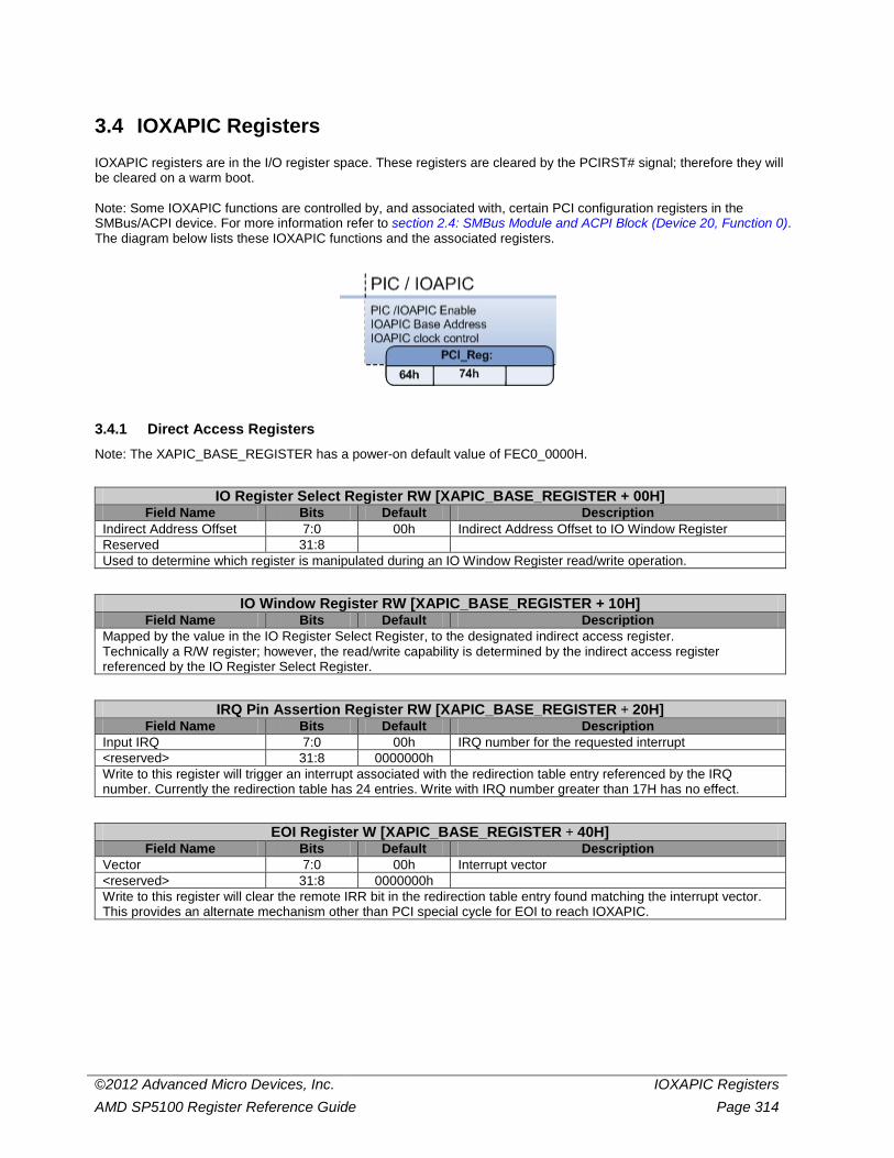
©2012 Advanced Micro Devices, Inc. IOXAPIC Registers AMD SP5100 Register Reference Guide Page 314
3.4 IOXAPIC Registers IOXAPIC registers are in the I/O register space. These registers are cleared by the PCIRST# signal; therefore they will be cleared on a warm boot. Note: Some IOXAPIC functions are controlled by, and associated with, certain PCI configuration registers in the SMBus/ACPI device. For more information refer to section 2.4: SMBus Module and ACPI Block (Device 20, Function 0). The diagram below lists these IOXAPIC functions and the associated registers.
3.4.1 Direct Access Registers Note: The XAPIC_BASE_REGISTER has a power-on default value of FEC0_0000H.
IO Register Select Register RW [XAPIC_BASE_REGISTER + 00H] Field Name Bits Default Description
Indirect Address Offset 7:0 00h Indirect Address Offset to IO Window Register Reserved 31:8 Used to determine which register is manipulated during an IO Window Register read/write operation.
IO Window Register RW [XAPIC_BASE_REGISTER + 10H] Field Name Bits Default Description
Mapped by the value in the IO Register Select Register, to the designated indirect access register. Technically a R/W register; however, the read/write capability is determined by the indirect access register referenced by the IO Register Select Register.
IRQ Pin Assertion Register RW [XAPIC_BASE_REGISTER + 20H] Field Name Bits Default Description
Input IRQ 7:0 00h IRQ number for the requested interrupt <reserved> 31:8 0000000h Write to this register will trigger an interrupt associated with the redirection table entry referenced by the IRQ number. Currently the redirection table has 24 entries. Write with IRQ number greater than 17H has no effect.
EOI Register W [XAPIC_BASE_REGISTER + 40H] Field Name Bits Default Description
Vector 7:0 00h Interrupt vector <reserved> 31:8 0000000h Write to this register will clear the remote IRR bit in the redirection table entry found matching the interrupt vector. This provides an alternate mechanism other than PCI special cycle for EOI to reach IOXAPIC.
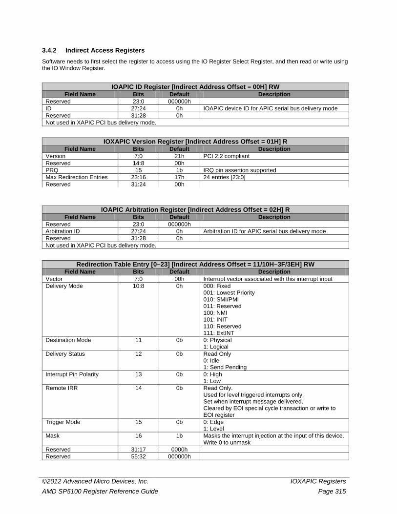
©2012 Advanced Micro Devices, Inc. IOXAPIC Registers AMD SP5100 Register Reference Guide Page 315
3.4.2 Indirect Access Registers Software needs to first select the register to access using the IO Register Select Register, and then read or write using the IO Window Register.
IOAPIC ID Register [Indirect Address Offset = 00H] RW Field Name Bits Default Description
Reserved 23:0 000000h ID 27:24 0h IOAPIC device ID for APIC serial bus delivery mode Reserved 31:28 0h Not used in XAPIC PCI bus delivery mode.
IOXAPIC Version Register [Indirect Address Offset = 01H] R Field Name Bits Default Description
Version 7:0 21h PCI 2.2 compliant Reserved 14:8 00h PRQ 15 1b IRQ pin assertion supported Max Redirection Entries 23:16 17h 24 entries [23:0] Reserved 31:24 00h
IOAPIC Arbitration Register [Indirect Address Offset = 02H] R Field Name Bits Default Description
Reserved 23:0 000000h Arbitration ID 27:24 0h Arbitration ID for APIC serial bus delivery mode Reserved 31:28 0h Not used in XAPIC PCI bus delivery mode.
Redirection Table Entry [0–23] [Indirect Address Offset = 11/10H–3F/3EH] RW Field Name Bits Default Description
Vector 7:0 00h Interrupt vector associated with this interrupt input Delivery Mode 10:8 0h 000: Fixed
001: Lowest Priority 010: SMI/PMI 011: Reserved 100: NMI 101: INIT 110: Reserved 111: ExtINT
Destination Mode 11 0b 0: Physical 1: Logical
Delivery Status 12 0b Read Only 0: Idle 1: Send Pending
Interrupt Pin Polarity 13 0b 0: High 1: Low
Remote IRR 14 0b Read Only. Used for level triggered interrupts only. Set when interrupt message delivered. Cleared by EOI special cycle transaction or write to EOI register
Trigger Mode 15 0b 0: Edge 1: Level
Mask 16 1b Masks the interrupt injection at the input of this device. Write 0 to unmask
Reserved 31:17 0000h Reserved 55:32 000000h

©2012 Advanced Micro Devices, Inc. IOXAPIC Registers AMD SP5100 Register Reference Guide Page 316
Redirection Table Entry [0–23] [Indirect Address Offset = 11/10H–3F/3EH] RW Field Name Bits Default Description
Destination ID 63:56 0 Bits [19:12] of the address field of the interrupt message

©2012 Advanced Micro Devices, Inc. Revision History AMD SP5100 Register Reference Guide Page 317
Appendix A: Revision History
Date Rev. Comment August, 2012 3.03 2.4.3.2: Power Management (PM) Registers:
Updated WatchDogTimerControl [PM_Reg:69h] 2.3.4 USB1/ USB2 EHCI PCI Configuration Registers:
Updated EHCI Misc Control [PCI_Reg: 50h] January, 2011 3.02 Update to register EHCI Misc Control [PCI_Reg: 50h] -- added bit[26] description. November, 2010 3.00 Public release based on internal version rev 2.07.