AGA AW - The Stanford University...
36
Transcript of AGA AW - The Stanford University...

PPP:
A GATE-LEVEL POWER SIMULATOR
A WORLD WIDE WEB APPLICATION
Alessandro Bogliolo
Luca BeniniGiovanni De Micheli
Bruno Ricc�o
Technical Report: CSL-TR-96-691
March 1996
This work was partially supported by NSF (under contract MIP-9421129)
and by AEI (under grant De Castro)


i
PPP: A Gate-Level Power Simulator
A World Wide Web Application
Alessandro Bogliolo Luca Benini Giovanni De Micheli Bruno Ricc�o1
Technical Report: CSL-TR-96-691
March 1996
Computer Systems Laboratory
Departments of Electrical Engineering and Computer Science
Stanford University
Stanford, CA 94305-9040
Abstract
Power consumption is an increasingly important constraint for complex ICs. Accurate and
e�cient power estimations are required at any level of abstraction to steer the design process.
PPP is a Web-based integrated environment for synthesis and simulation of low-power CMOS
circuits. We describe the simulation engine of PPP and we propose a new paradigm for tool
integration.
The simulation engine of PPP is a gate-level simulator that achieves accuracy comparable
with electrical simulation, while keeping performance competitive with traditional gate-level
techniques. This is done by using advanced symbolic models of the basic library cells, that
exploit the understanding of the main phenomena involved in power consumption. In order
to maintain full compatibility with gate-level design tools, we use VERILOG-XL as simulation
platform. The accuracy obtained on benchmark circuits is always within 6% from SPICE also
for single-gate/single-pattern power analysis, thus providing the local information needed to
optimize the design.
Interface and tool integration issues have been addressed using a Web-based approach. The
graphical interface of PPP is a dynamically generated tree of interactive HTML pages that allow
the user to access and execute the tool through the Internet by using his/her own Web-browser.
No software installation is required and all the details of data transfer and tool communication
are hidden to the user.
Key Words and Phrases: Power consumption, Symbolic gate model, Gate-level simulation,
CAD tool integration, Web-based application
1With the DEIS, University of Bologna, viale Risorgimento 2, 40135 Bologna, Italy.

Copyright c 1996
Alessandro Bogliolo, Luca Benini, Giovanni De Micheli and Bruno Ricc�o

iii
Contents
1 Introduction 1
2 Gate-Level Power Simulation 2
2.1 Cell-Based Power Simulation : : : : : : : : : : : : : : : : : : : : : : : : : : : : : 3
3 A New Approach 5
3.1 Basic Idea : : : : : : : : : : : : : : : : : : : : : : : : : : : : : : : : : : : : : : : : 5
3.2 Advanced Gate Models : : : : : : : : : : : : : : : : : : : : : : : : : : : : : : : : : 6
3.3 Evaluating Ec : : : : : : : : : : : : : : : : : : : : : : : : : : : : : : : : : : : : : : 6
3.4 Evaluating Ew : : : : : : : : : : : : : : : : : : : : : : : : : : : : : : : : : : : : : 8
3.5 Multiple Transitions : : : : : : : : : : : : : : : : : : : : : : : : : : : : : : : : : : 8
3.6 Timing Information : : : : : : : : : : : : : : : : : : : : : : : : : : : : : : : : : : 10
3.7 Sequential Elements : : : : : : : : : : : : : : : : : : : : : : : : : : : : : : : : : : 11
3.7.1 Static Sequential Elements : : : : : : : : : : : : : : : : : : : : : : : : : : 11
3.7.2 Dynamic Elements : : : : : : : : : : : : : : : : : : : : : : : : : : : : : : : 12
3.8 Implementation : : : : : : : : : : : : : : : : : : : : : : : : : : : : : : : : : : : : : 13
4 Web-Based Tool Development 13
4.1 Motivations and Background : : : : : : : : : : : : : : : : : : : : : : : : : : : : : 13
4.2 The PPP Paradigm : : : : : : : : : : : : : : : : : : : : : : : : : : : : : : : : : : : 14
5 Tool Architecture 16
5.1 Application Layer : : : : : : : : : : : : : : : : : : : : : : : : : : : : : : : : : : : : 16
5.2 Communication Layer : : : : : : : : : : : : : : : : : : : : : : : : : : : : : : : : : 17
5.3 Interface Layer : : : : : : : : : : : : : : : : : : : : : : : : : : : : : : : : : : : : : 18
5.4 Bandwidth management : : : : : : : : : : : : : : : : : : : : : : : : : : : : : : : : 18
5.5 Implementation Details : : : : : : : : : : : : : : : : : : : : : : : : : : : : : : : : 19
6 PPP User Session 20
6.1 Circuit Speci�cation and Mapping : : : : : : : : : : : : : : : : : : : : : : : : : : 21
6.2 Simulation Setup : : : : : : : : : : : : : : : : : : : : : : : : : : : : : : : : : : : : 22
6.3 Power Simulation : : : : : : : : : : : : : : : : : : : : : : : : : : : : : : : : : : : : 24
7 Experimental Results 25
8 Conclusions and Future Work 27
9 Acknowledgements 28


Introduction 1
1 Introduction
Power dissipation in VLSI systems has recently become a critical metric for design evaluation.
A large number of power estimation techniques have been recently proposed [1, 2, 3, 4], based on
models at di�erent levels of abstraction, ranging from electrical level to architectural level [5, 6,
7]. Electrical-level simulators produce the most accurate results, but are often very demanding
in terms of computational resources. Moreover, the large number of simulations needed to reach
a reliable estimate of average power dissipation further restricts the class of circuits that can be
analyzed with electrical simulators in a reasonable time.
At a higher level of abstraction, logic-level simulation allows power estimation for very large
blocks, often enabling full-chip simulation. As a consequence, for CMOS digital circuits, logic-
level simulation is usually the preferred tool for validation and debugging, and the large majority
of designers is highly familiar with logic simulation tools. Mainly for these reasons, many
attempts have been made to provide power estimation at the logic level. In the simplest model,
power is estimated observing the switching activity at the output of the basic logic blocks of
the circuit (weighted by the load capacitance). The advantage of this model is that it enables
the application of pattern independent techniques, which provide an estimate of the average
switching activity without actually simulating the circuit with a large number of test patterns
[2].
Power estimation based on switching activity has however limited accuracy, mainly because it
does not consider phenomena such as non-instantaneous signal transitions, spurious transitions
(glitches) and gate internal capacitances, that may have a sizable impact on the total power
dissipation. In order to overcome these di�culties, advanced logic simulation techniques have
been proposed that allow increased accuracy, while maintaining the abstraction at the logic level
[8, 9, 10]. In these approaches, lookup tables are obtained by electrical simulation of the basic
building blocks, and the collected data are then used during gate-level simulation.
Although these techniques reported promising results, they have two main limitations. First,
they do not assume any model for the internal structure of the basic building blocks (gates).
Second, they do not deal with multiple input transitions that are not perfectly aligned in time,
with misalignments smaller than the propagation delay of the gate. In this work we propose a
more accurate model based on the structure of the gate (and on the physical understanding of
the electrical phenomena involved in power dissipation) that overcomes the limitations above
mentioned, while keeping computational e�ciency competitive with traditional gate-level power
simulation.
Our technique exploits a BDD-based symbolic model for describing the charge and discharge
of parasitic (and load) capacitances and the ow of short circuit current. Lookup tables are
used only for modeling the timing behavior of the circuit (as it is commonly done in full-delay
simulation), therefore power simulation only marginally increases the memory usage. Our model
is exible and can be used to accurately estimate power dissipation for gates in a large range of

2 CSL-TR-96-691
load and input conditions. As a result, our method is highly accurate also for single gate (local)
power estimate, allowing the individuation of critical gates during design optimization.
We have implemented our algorithms using VERILOG-XL as simulation platform, therefore
maintaining full compatibility with design environments based on VERILOG HDL. For our test
library the accuracy on local power estimation is within 6% from SPICE under a wide range
of fan-in and fan-out conditions, while the accuracy on the average power dissipation for large
benchmarks is even higher. The speed penalty with respect to unit-delay VERILOG simulation
is within a factor of 6, while the speedup with respect to fast SPICE simulation ranges from two
to three orders of magnitude.
We have used our simulator as the starting point for the development of a CAD tool that we
called PPP. PPP has been conceived as an integrated environment for simulation and synthesis
of low-power CMOS circuits. Its main features are modularity, machine independence, resource
distribution and remote execution. All these features are implemented by following a new tool
integration and interfacing paradigm based on the World Wide Web. The graphical interface
of PPP is a net of interactive HTML pages that can be accessed through the Internet using
traditional Web-browsers.
In the next section we discuss the main issues involved in gate-level power simulation. In
section 3 we introduce our model of power consumption in CMOS gates and we describe how to
use it in an event-driven simulation context. In section 4 we introduce the PPP-paradigm for
Web-based tool integration and interfacing. The architecture of PPP is then described in section
5 and a typical user session is exempli�ed in section 6. In section 7 we report the experimental
results obtained on a large set of benchmark circuits and in section 8 we draw conclusions.
2 Gate-Level Power Simulation
Traditional gate-level power estimates are based on the simplifying assumption that the supply
current required by a CMOS circuit is essentially spent on charging load capacitances at the
outputs of the switching gates. Because of this assumption, the inner structure of the gates is
neglected and the average power consumption is evaluated simply by looking at the switching
activity (toggle count) and the capacitive load at the gate outputs.
In this way, however, the actual power consumption can be heavily underestimated since
several parasitic phenomena (such as short-circuit currents, charging and discharging of internal
capacitances and charge sharing) that may have a sizable impact on the global power, cannot
be captured.
Example 1 Fig. 1 represents a CMOS realization of a three inputs OR gate. Starting from the
input con�guration x = 100, consider a transition of the input signal x1 from 1 to 0 (boldfacing
is hereafter used to denote Boolean vectors: x = [x1x2x3]). The only e�ect of this transition that
can be captured at logic level is the discharging of CL, that does not cause any current from power

Gate-Level Power Simulation 3
2
CL
1C
CL
x1 x2 x3
x1
x2
x3
x1
x3
x2
Vdd
C
C3
out
Vdd
Vdd
outOR
11
2
3
n V
V2
3V
n
n n V4 4
Figure 1: CMOS realization of a three input OR gate. Parasitics are modeled by means of four constant
capacitors to ground: C1 = C2 = 11fF , C3 = 157fF and CL = 136fF .
supply. However, a sizable power is actually drawn by the gate due to the charging of internal
capacitances and to the presence of transient conductive paths from power-supply to ground. In
particular, the power consumption is of 0.22mW (according to HSPICE) for an input transition
of 0.1ns and a clock period of 20ns. This is of the same order of the supply power required for
a rising transition of the output node, even with an additional load of 50fF . 2
Moreover, spurious transitions (glitches) that may represent the 20% of the switching activity
[11], cannot be accurately accounted for, due to the use of simpli�ed cell delay models.
Example 2 At a logic level of abstraction, changing the inputs of the OR gate of Fig. 1 from
x = 100 to x = 010 does not cause any e�ect. However, a misalignment between the falling and
rising edges of input signals x1 and x2 (i.e., x2 rising 0.4ns after x1 has fallen), may give rise to
a power consumption of 0.08mW (according to HSPICE), because of two phenomena (see Fig.
1):
i) a double, spurious transition (glitch) at the output node, causing the charging/discharging
of both CL and C3, and
ii) short-circuit currents through both the CMOS stages. 2
In principle, the above mentioned limitations can be overcome by taking advantage, during
gate-level simulation, of previously collected information about the basic building blocks of the
circuit.
2.1 Cell-Based Power Simulation
Cell-based power estimation [8] improves upon simple logic-level estimation and consists of the
two steps paradigm of cell characterization and logic simulation. The characterization phase
includes a set of electrical simulations of each library-cell for all possible input transitions and

4 CSL-TR-96-691
for a wide range of fan-in and fan-out conditions. Timing and power information obtained in
this way is used to construct lookup tables for each library-cell.
Logic simulation is then performed by a back-annotated event-driven simulator. Whenever
a transition occurs at the input of a gate, both the propagation delay and the energy drawn by
the gate are read on the corresponding lookup tables. Notice that during simulation, the gate
is seen as a black-box, no information about its internal structure and status is exploited.
In principle, as long as the lookup tables have entries corresponding to the actual fan-in/fan-
out conditions of each gate of the circuit, the back-annotated gate-level simulation reaches the
accuracy of the electrical one. However, the power consumption and the propagation delay of
library cells cannot be pre-characterized for all possible transitions and for all possible values of
parameters they depend on (input slopes and skews, output loads). In practice, instead, electrical
simulations are performed only for single input transitions and for a given set of typical values
of the I/O parameters, thus reducing both the number of electrical simulations and the size of
the lookup tables. The subsequent discretization ultimately impairs the accuracy of the power
estimate. On the other hand, the results of electrical simulations are not accurately �t by any
elementary algebraic function of input patterns and I/O parameters.
Moreover, the power consumption of a CMOS cell actually depends on the charge status of
its internal capacitances, that is usually neglected in the context of gate-level simulation, giving
rise to further approximations.
Example 3 With respect to Fig. 1, consider a transition from x = 101 to x = 001. The actual
energy drawn by the OR gate corresponding to this input transition depends on the charge status
of its internal capacitances. In particular, no supply energy is required if both C1 and C2 have
already been charged at Vdd by a previously applied input vector x = 001, while otherwise 0.44pJ
(22�W with a 20ns cycle-time) are dissipated. Hence, internal voltages should also be taken into
account in order to obtain accurate power estimates. 2
Recently, more re�ned methods have been proposed that partially exploit the knowledge
of the power consuming phenomena inside the cells. In [10] it is observed that the power
dissipated by a cell is characterized by two radically di�erent behaviors depending on the ratio
between slope of the input and output transitions. If the ratio is larger than one, short circuit
current becomes important, while if it is smaller this contribution is less relevant. Based on
this observation, a model is proposed in which two di�erent �tting formulas are used depending
on the above mentioned ratio. The accuracy in this approach is limited by the simple analytic
model and the by lack of information on the internal state of the cells.
In [9] a �nite-state machine (FSM) model for the cell is proposed, in which the internal charge
status of the gate is modeled, and the power dissipated during input transitions is represented by
weights associated with the state transitions of the FSM. However, the power dissipated during a
transition depends not only on the initial and �nal charge status, but also on the capacitive load
A New Approach 5
and on the slope of input and output transitions. This dependency is not explicitly modeled,
thus requiring the use of (large) lookup tables associated with each transition.
Moreover, both techniques do not model accurately signal waveforms, multiple misaligned
input transitions and parasitic phenomena causing intermediate voltage levels (such as signal
glitches and charge sharing). In the next section, we present a new cell-based approach that
overcomes the above limitations.
3 A New Approach
As mentioned before, cell-based power estimation techniques must compromise between the size
of the lookup tables and the accuracy of the estimates. In order to obtain a better trade-o�
between e�ciency and accuracy, we use an advanced model of power consumption in CMOS
cells, based on the understanding of the electrical phenomena involved.
3.1 Basic Idea
In principle, the supply current I(t) drawn by a CMOS cell corresponding to an input transition
(namely, from xi to xf) can be viewed as consisting of two contributions:
� a charging current Ic(t), that increases the total charge of internal and load capacitors,
and
� a wasted current Iw(t), that does not a�ect the charge status of the cell.
The energy drawn by the cell during the whole transition can accordingly be partitioned into
two contributions:
Ec =Z
tf
ti
VddIc(t)dt; Ew =Z
tf
ti
VddIw(t)dt:
Apexes i and f are hereafter used to denote the beginning and the end of a given transition,
respectively.
In general, even if we run accurate electrical simulations, we cannot distinguish between the
two portions of supply current (Ic and Iw). However, we can evaluate Ec simply by looking at
the charge status of the cell. In fact, since I = dq
dt, Ec can be expressed as
Ec = Vdd
Ztf
ti
Ic(t)dt = Vdd �Q; (1)
where �Q is the total charge provided by Vdd to internal and load capacitors. �Q can therefore
be computed by the following equation:
�Q =Xj2S
�qj ; (2)

6 CSL-TR-96-691
where S is the set of connected nodes with a connection to Vdd for input vector xf , and �qi
is the charge increase at node ni: �qj = Cj(Vf
j� V i
j). It is worth noting that Ec does NOT
depend on the I/O parameters, and its computation ultimately requires only the knowledge of
the charge status (or voltage level) at each node of the cell.
The wasted energy (Ew = E � Ec), on the other hand, does NOT depend on the internal
charge status, and can be approximated by a (linear) function of the I/O parameters, obtained
by �tting the results of electrical simulations.
3.2 Advanced Gate Models
For each cell, we provide the layout-extracted internal capacitances and we model the parasitics
with constant capacitors to ground, as shown in Fig. 1. We denote by N the ordered set of cell
nodes (n1; n2; :::; nN), including primary outputs, and by Ci the capacitance between node ni
and ground.
In order to compute Ec, we need to know the voltage level at each node at the beginning and
at the end of any transition. Moreover, we need to dynamically determine the set (S) of nodes
connected to power supply. To solve these problems, we keep track of the Boolean conditions
enabling the connection of each node to ground (Vss), to Vdd and to each other node in the cell.
These conditions make up a connection matrix M(x), with N rows and N columns
associated with the cell nodes: entry mi;j(x) of the matrix is a Boolean function of the cell
inputs, taking value 1 for those input con�gurations for which a conductive path exists between
nodes ni and nj . Two additional columns (namely N + 1 and N + 2) are used to represent the
connectivity to power supply (d) and ground (s).
Example 4 For the OR gate of Fig. 1, the elements of the �rst row of the connection matrix
are: m1;1(x) = 1, m1;2(x) = x02, m1;3(x) = x0
2x03, m1;4(x) = 0, m1;d(x) = x0
1, and m1;s(x) =
x1(x2 + x3). The output node is denoted by n4. 2
The e�cient handling of the connection matrix is obtained by using Reduced Ordered Binary
Decision Diagrams (BDDs) to represent Boolean functions [12]. To this purpose notice that the
square sub-matrix consisting of the �rstN columns ofM(x) is symmetrical, and the BDD-based
representation allows a consistent amount of sharing among its entries.
It is also worth noting thatM(x) is constructed only once for all, during the characterization
phase. At run-time, for each input pattern x the connection status is then obtained fromM(x)
in linear time, by simple BDD evaluations.
3.3 Evaluating Ec
During logic simulation, the connection matrix is used both to compute Ec and to update the
charge status. In particular, the total charge provided by power supply to the internal and load

A New Approach 7
capacitors can be easily evaluated using the column of M associated with Vdd. For a generic
cell with N nodes (including primary output nodes), Equation (2) can be rewritten as:
�Q =NXi=1
mi;d(xf)Ci(V
f
i� V i
i): (3)
Example 5 With respect to Fig. 1, the Boolean conditions enabling the connection of each
node of the OR gate to power supply are: m1;d(x) = x01, m2;d(x) = x0
1x02, m3;d(x) = x0
1x02x03,
m4;d(x) = x1 + x2 + x3. For instance, the charge provided by Vdd when the cell inputs switch to
xf = 011 is then expressed by:
�Q = C1(Vf
1 � V i
1) + C4(V
f
4 � V i
4);
where C4 corresponds to the output load CL. 2
Equation (3) requires the complete knowledge of node voltages at the beginning and at the
end of the transition. Node voltages are updated by exploiting the connection matrix:
Vf
i= mi;d(x
f)Vdd +mi;s(xf)Vss +mi;float(x
f)
PN
j=0mi;j(xf)CjV
i
jPN
j=0mi;j(xf)Cj
; (4)
where mi;float(xf) takes value 1 whenever node ni is oating: mi;float = m0
i;dm0
i;s. In practice,
mi;d(x), mi;s(x) and mi;float(xf) work as mutually exclusive selection functions:
� if ni is connected to power supply (mi;d = 1), the new value of Vi is Vdd;
� if ni is connected to ground (mi;s = 1), the new value of Vi is Vss;
� if ni is oating (mi;float = 1), the new value of Vi is computed by taking into account the
charge sharing with other channel-connected nodes.
Example 6 Consider a transition to xf = 101 at the inputs to the OR gate of Fig. 1. At the
end of the transition, node n1 is oating and connected only to n2. So, the new value of V1 is
given by the charge sharing between n1 and n2:
Vf
1 =C1V
i
1 + C2Vi
2
C1 + C2
:
2
Notice that Equation (4) also allows us to take implicitly into account the e�ect of threshold
drop on the voltage levels of internal nodes connected to Vdd (Vss) through n-channel (p-channel)
transistors [13]. For a generic node (say, ni) this is done simply by replacing the nominal values
of Vdd and Vss, with values obtained from electrical simulations (namely, Vddi and Vssi) taking
into account transistor threshold drops.
The main source of error in our estimation of Ec is then the constant capacitor to ground
model ( oating capacitors are modeled as capacitors to ground). The e�ect of nonlinear time-
varying junction capacitances and feedthrough parasitic capacitances are approximatively ac-
counted for in the Ew component of energy dissipation.

8 CSL-TR-96-691
3.4 Evaluating Ew
The main contribution to Ew is due to the presence of short circuit currents from power supply to
ground. The connection matrix can be used to detect conditions for which there is a transient
open path between Vdd and Vss. In practice, a wasted current is drawn from power supply
whenever a node that was connected to Vdd for input vector xi is connected to Vss for input
vector xf , or viceversa. For a generic cell with N nodes, this condition is expressed by
fw(xi;xf) =
NXi=1
[mi;d(xi)mi;s(x
f) +mi;s(xi)mi;d(x
f)]: (5)
If fw = 0, then Ew = 0; if fw = 1, instead, Ew depends on fan-in and fan-out conditions,
represented by the input slopes S1; :::; Sn and by the output load CL. Corresponding to any
transition, however, short circuit currents are not in uenced by those input (output) parameters
associated with input (output) signals that don't change.
Since there are no simple closed-form models for the wasted contribution to power consump-
tion, we approximate Ew with a �rst-order function of the I/O parameters:
Ew = fw(c1S1 + :::+ cnSn + cn+1foutCL); (6)
where fout is a Boolean ag taking value 1 corresponding to output transitions (fout = out(xf )�
out(xi)), and the input slopes are set to 0 if the corresponding inputs do not change (xfi=
xii=) Si = 0). Pattern dependency is thus implicitly accounted for.
Coe�cients c1; :::; cn+1 are computed with min-square �tting of values obtained by circuit
simulation. It is important to notice that the computation of Ew requires a number of �tting
coe�cients that is linear in the number of inputs and outputs of the cell.
3.5 Multiple Transitions
Although the model described above is accurate for perfectly aligned multiple input transitions,
this assumption is often violated in practice. In the majority of cases, multiple input transitions
are slightly misaligned, possibly by short times (compared to the transition time of the gate).
In this case a model that computes the power dissipation observing single input transitions
may produce large errors, because it will consider a slightly misaligned multiple transition as a
sequence of full transitions.
Assume that a two input transition from input pattern xi to xf is not perfectly aligned.
The misalignment causes an intermediate pattern (say, xm) to appear at the input of the gate
for a short period of time. Assume � to be the delay between the misaligned input transitions
(i.e., the input skew). We call transient time the time Ti!m needed to reach 90% of the total
charge transfer from Vdd to capacitances in the gate (caused by the transition xi ! xm). There
are two limit situations:

A New Approach 9
0e+00 2e-09 4e-09Input Skew (sec)
0e+00
4e-12
8e-12
Ene
rgy
(J)
HSPICEOur method
Figure 2: E�ect of the input skew on the energy drawn by a three inputs OR gate corresponding to an input
transition from xi = 100 to x
f = 011.
� If � << Ti!m, pattern xm does not appear at the inputs and the energy dissipated is
E = Ei!f .
� On the other hand, if � > Ti!m, we have two complete transitions and the total energy
dissipation is E = Ei!m +Em!f .
We approximate the intermediate cases using a linear interpolation between the two limits,
as shown in Fig. 2. Namely:
E = (Ei!m + Em!f)�
Ti!m
+Ei!f(1��
Ti!m
): (7)
Clearly this formula holds if � < Ti!m, while if this is not true we have E = Ei!m + Em!f .
Example 7 Consider the OR gate of Fig. 1, and assume that a multiple input transition occurs
from xi = 100 to xf = 011, with a misalignment (�) of 1ns between the falling edge of x1 and
the rising edges of x2 and x3. As shown in Fig. 3.a, the input misalignment gives rise to an
intermediate input pattern xm = 000. By electrical simulation, the total energy drawn by the
cell is of 4:15pJ.
Since the transient time (Ti!m = 1:7ns) is greater than the input skew (� = 1ns), to evaluate
E at logic level we refer to the two limit situations of simultaneous and disjoint input transitions
(Figg. 3.b and 3.c), providing:
Ei!f = 0:41pJ,
Ei!m = 4:42pJ, Em!f = 3:37pJ,

10 CSL-TR-96-691
x2x3
x1
τ
t
Vx2x3
x1
x2x3
x1
i mT
100
00
0 011
100
100
100
00
0011
011
00
0
i mTτ
V1
V2
V3
V1
V2 V3
V1V2
V3 V3
V2
V1
i mTτ ttt t
VVVV
a) b) c) d)
011
t
V
t
V τ
t
V
x1
x2x3
Figure 3: a) Symbolic representation of the e�ects of a misaligned multiple transition on the internal voltages
of the OR gate of Fig. 1. At logic level, we can handle only the two limit situations of b) perfectly aligned input
edges, and c) sequences of completely disjoint transitions. However, good estimates of the internal voltages can
be obtained in any other case (d) by means of linear interpolation.
respectively. The actual energy estimate is then provided by the following linear interpolation:
E = 0:41(1�1
1:7) + (4:42 + 3:37)
1
1:7pJ = 4:58pJ;
with an error of 4:8% from SPICE. 2
The same approach is used to approximate the charge status of the cell at the end of slightly
misaligned multiple transitions, as shown in Fig. 3.d.
The linear approximation is obviously exact at the boundaries, but its accuracy depends on
the de�nition of Ti!m. In general, Ti!m is strongly pattern dependent and it is not equal to the
delay used for event propagation. This is shown in the next section.
3.6 Timing Information
As mentioned in previous sections, the power drawn by a cell depends not only on the input
patterns applied, but also on signal waveforms and arrival times. At the logic level, however,
signal slopes are neither represented nor propagated, and simple delay models (such as unit
delay) are used for scheduling the events. These approximations have a critical impact on the
accuracy of power estimates.
To solve this problem, we provide accurate models of the three main parameters representing
the time behavior of each library-cell:
� the propagation delay D (used by the simulator for the event scheduling),
� the output slope Sout (used for power estimation of the driven gates),
� the transient time T (used to handle misaligned multiple transitions).

A New Approach 11
0
10
1
x 2
x 1
LATCH1
LATCH2
D
CLK
Q
Figure 4: Static implementation of an edge triggered D register composed of two level sensitive latches.
We approximate these parameters with pattern-dependent functions of both the output load
(CL) and the average input slope (Savg):
D = c0d(x) + c1d(x)Savg + c2d(x)CL;
Sout = c0s(x) + c1s(x)Savg + c2s(x)CL; (8)
T = c0t(x) + c1t(x)Savg + c2t(x)CL:
The pattern dependent coe�cients c are determined by means of electrical simulations during
the library characterization phase: for each �nal input con�guration xf a set of min-square �tting
coe�cients is obtained.
In principle, we obtain 2n di�erent values for each coe�cient. In practice, however, the
majority of them do not change within large sets of input con�gurations. Hence, the number
of possible assignements of the �tting coe�cients is usually small and their pattern dependence
can be e�ciently modeled by means of ADDs [14].
3.7 Sequential Elements
In order to describe the model of power consumption in CMOS gates, we have always referred to
a static combinational cell (namely, a CMOS implementation of a three input OR gate). In this
section we remove this restriction by extending the approach to static and dynamic sequential
elements.
3.7.1 Static Sequential Elements
The gate-level representation of a static sequential circuit is always characterized by the presence
of feedback signals. Consider the edge triggered register of Fig. 4. At gate level, it can be
represented either as a net of six interconnected combinational elements (four inverters and two
multiplexers) with two external feedbacks (x1 and x2), or as a sequence of two latches (LATCH1
and LATCH2) with internal feedback.
In the �rst case no change is required. Our gate model is directly applied to each component,
while feedback signals are explicitly handled by the event scheduling mechanism provided by

12 CSL-TR-96-691
n2n
n
n 3
4
5
6 7nnn 1
CLK
DQ
Figure 5: Dynamic CMOS implementation of an edge triggered D register.
the simulation platform (needless to say, the initial state of the sequential elements has to be
speci�ed in order to obtain signi�cant simulation results).
In the second case, the whole latches need to be modeled as basic building blocks. We refer
to the negative level-sensitive latch of Fig. 4 (namely, LATCH1) with inputs D and CLK and
output x1. Because of the internal feedback, neither the functionality nor the connectivity of the
cell (i.e., the values of the connection matrix entries) can be inferred from the knowledge of the
current input pattern. Nevertheless, we want to express the connection matrix as a combinational
function of Boolean variables. To this purpose, the last value of the feedback signal (x1) is to
be considered as an additional control variable for the connection matrix: M(D;CLK; x1).
Notice that x1 is also the primary output of the cell, and there is a row of the connection
matrix associated with it. During simulation, the new value of x1 is then provided by the model
itself. The use of the same signal both as independent and as dependent variable is the implicit
representation of the internal feedback.
In general, the connection matrix of a sequential element will be a combinational function
of both primary inputs and feedback variables. This is the only extension required to deal with
sequential components.
3.7.2 Dynamic Elements
Dynamic CMOS logics exploit the memory e�ects associated with the charge retention at the
internal ( oating) nodes of a cell. On the other hand, in section 2.1 we remarked that the charge
status at the internal nodes of a CMOS cell may have a sizable impact on power consumption.
We then constructed a state-dependent symbolic model that takes into account charge retentions
at internal nodes. As a consequence, our cell model is inherently able to capture dynamic e�ects
associated with internal parasitic capacitances.
From a structural point of view, the only di�erence between static and dynamic CMOS logics
is that in dynamic logic oating nodes may be used to drive CMOS stages.
Example 8 Consider for instance the dynamic edge triggered register shown in Fig. 5. The
second CMOS stage is driven by internal node n2, that is oating when D = 0 and CLK = 1. In
Web-Based Tool Development 13
this case, neither the logic value of n2 nor the connectivity of the subsequent stage can be inferred
from the current values of D and CLK. Nevertheless, the charge status at n2 is provided by our
cell model, and the connectivity of the second CMOS stage can be expressed as a combinational
function of CLK and n2. 2
In general, to deal with dynamic cells we do not require additional information, but we
need to partition the connection matrix and change the sequence of steps involved in model
evaluation. In particular, the submatrices associated with cascaded stages must be evaluated in
sequence, in order to use partial results to drive the subsequent evaluations.
Example 9 For instance, the connection matrix of the �rst stage of the register shown in Fig.
5, is
m1;1 = 1 m1;2 = CLK0 m1;d = D0 m1;g = CLK 0D
m2;1 = CLK0 m2;2 = 1 m2;d = CLK0D0 m2;g = D
Whenever an input event occurs, the matrix is evaluated to obtain Vn2 from Eq. (4). Then, the
connection matrix of the second stage can be evaluated using n2 as input variable.
m3;4 = 1 m3;4 = n2 m3;d = n2CLK0 m3;g = CLK
m4;3 = n2 m4;4 = 1 m4;d = CLK0 m4;g = n2CLK2
In summary, the entries of the connection matrix associated with a generic (combinational
or sequential) CMOS cell may be functions of primary inputs, internal variables, and previous
values of feedback signals.
3.8 Implementation
Routines for both the construction of the connection matrix and the min-square �tting of elec-
trical simulations have been implemented in C using standard packages for BDD and matrix
manipulations. VERILOG-XL has been used as simulation platform. The pre-characterized
symbolic models of library cells have been written as C functions and made available from logic
simulation using the Programming Language Interface (PLI) of VERILOG-XL.
Our simulator has been used as the starting point for the development of PPP, a fully
integrated synthesis and simulation environment with short learning curve and architecture-
independent Web-based interface. The innovative aspects of the implementation of PPP are
described in the next section.
4 Web-Based Tool Development
4.1 Motivations and Background
The number of tools needed to implement complex systems is ever increasing, and such tools are
generally provided by a myriad of suppliers. Integration of EDA tools into uni�ed frameworks

14 CSL-TR-96-691
prompts for an increasing e�ort in the creation of standard interfaces [15, 16]. The de�nition
of standard formats for design descriptions such as VHDL and EDIF has been an important
milestone in this direction. However, the user interfaces provided by di�erent EDA vendors still
lack in uniformity and compatibility.
Moreover, as computer networking becomes pervasive, design teams will be geographically
dispersed, and the need for reliable and straightforward communication paradigms will steadily
grow. Computationally demanding tasks (optimization and/or simulation of large circuits) could
be performed on high-performance servers remotely connected to the designers by Internet links.
Again, a uniform user interface should be provided in this concurrent and distributed engineering
environment.
The opportunities for commercial EDA vendors are promising as well. New tool usage
paradigms may emerge: users could temporarily connect to a tool provider, perform a speci�c
task and be billed on a usage-time basis. Similarly, demos can be performed across the network, a
much more e�ective form of advertisement, because it gives the perspective user direct hands-on
experience. Necessary conditions for such new paradigms to be successful is again the existence
of a general and friendly user interface for remote connections and execution control.
The explosive di�usion of an user-friendly and powerful interface such as the World Wide
Web [17] (WWW) has prompted several attempts directed to exploit its features in the CAD-
EDA area. Virtually every computer user is familiar with the WWW, and Web browsers provide
an uniform interface to a number of di�erent communication protocols. A Web-based interface
to CAD tools is an important step toward standardization and distributed tool integration.
Preliminary results in this direction have been reported in [18] and [19]. In both this works
the designer's need for geographically disperse and heterogeneous information is addressed and
simple protocols for remote batch execution are described: the user can request services to remote
tools, that will perform the required tasks and return the results. The interaction between users
and tools is sparse and loose.
E�ective execution of remote tools requires a much higher level of interaction: the user
should be allowed to change the setting of a parameterized tool run, preview partial result,
access visual information like waveforms and network schematics, modify networks and update
design databases.
4.2 The PPP Paradigm
PPP has been conceived as a modular system composed of interacting tools that may run on
di�erent machines and be (possibly) provided by di�erent vendors or contributors. The main
target of PPP is the synthesis and the simulation of low-power CMOS circuits, but its modularity
allows us to interface with general-purpose commercial and academic tools.
The user accesses PPP using his/her own Web browser, with no additional requirements on
hardware or software installation. The tools can reside on remote servers or on the local machine.

Web-Based Tool Development 15
PPPBrowser
Database
Tool
WWW
CLIENT SERVER
Kernel
Figure 6: User interaction with PPP
This is fully transparent to the user. The graphical user interface (GUI) of PPP is exactly the
same used for Web navigation and no additional e�ort needs to be spent in familiarizing with a
new GUI when the user �rst accesses the system.
In the design of PPP, we focused on two key ideas: plug-and-play modularity and architecture-
independent interactive remote execution. Plug-and-play modularity allows new tools to be
integrated in PPP with little e�ort and no modi�cations. The impact on other tools already
embedded in the environment is negligible. Remote execution can be seen as an advanced
caching strategy. Upon invocation, a resource in PPP can maintain its state throughout a se-
quence of interactions. The state information is not necessary saved on �les to avoid the penalty
of iterated disk accesses (or, worse, of sending data across the Internet), but it is kept in memory
because the resource does not terminate its execution after every interaction with the user.
From the user's point of view, PPP appears as a remote HTTP server and each user can
access it by simply inserting a pointer to the PPP URL in his/her bookmark �le. This is
the only setup operation required. Figure 6 represents the user interaction with PPP. The
rectangles denote di�erent machines connected to the Internet. PPP is the core of a distributed
architecture. It manages two di�erent kinds of interface: connection to the client and connection
to the resources (tools and databases). The arrows represent Internet protocols (FTP, HTTP,
mail, etc).
Multiple users are allowed to concurrently access PPP, similarly to a traditional WWW
server. Figure 6 depicts a centralized structure. The PPP kernel manages all interactions
between the users and the tools. In the next section we will describe the organization of the
PPP kernel and the overall architecture.

16 CSL-TR-96-691
USERS
APPLICATION
COMMUNICATION
INTERFACE High Bandwidth (images)
Low Bandwidth (menu choices)
Security
Load Control
Format Conversion
Res
ourc
e 1
Res
ourc
e 2
Res
ourc
e 3
Res
ourc
e 4
Res
ourc
e 5
Res
ourc
e 6
Figure 7: The layered architecture of PPP. Resources represented with shaded rectangles require an high degree
of interactivity.
5 Tool Architecture
PPP is build upon a layered architecture, following a well-known software engineering paradigm.
The three layers are: application, communication and interface. The organization of PPP is
shown in Figure 7. The top two layers are embedded in the kernel, while the application layer
is distributed. Application is at the bottom of the hierarchy and manages the interaction with
the tools and the information sources.
5.1 Application Layer
The synthesis and simulation tools embedded in PPP represent the bulk of the application
layer and are called resources. No constraint is posed on the target architecture and on the
programming language used for the implementation of the resources. The resources may run
on di�erent machines. Two levels of interaction between resources and the above layers are
possible. The simplest interaction is stateless connection: the tool performs some manipulation
on the input data, produces an output and terminates the execution. Stateless connection is
not truly stateless, because the information about previous invocations may be stored in �les.
Nevertheless, retrieving the state from �les imposes heavy performance penalties when highly
interactive operation is required (for example, during an user-controlled optimization session).
Stateless connection resembles the batch execution features described in [18, 19].
For applications where higher interactivity is required, we provide a novel paradigm called
interactive remote execution. Once started, the resource does not terminate its execution after
every command, but it simply waits for another command to be issued. The resource becomes
a server that awaits for service requests from the client (the user) keeping complete information

Tool Architecture 17
about past requests and their results. Resources that provide interactive remote execution must
satisfy some requirements on their external interface. In particular, it must be possible to
interactively receive data from another process without terminating the execution. Interactive
remote execution is required for running optimization and validation tools that perform user-
assisted tasks.
Example 10 An application requiring interactive remote execution is logic optimization, where
the user can decide among di�erent optimization strategies by observing the quality of interme-
diate results. In contrast, a long simulation is a typical example of batch execution. After setting
up the simulation parameters, the user dispatches the run and does not need to interact with the
tool until the run terminates.
5.2 Communication Layer
The communication layer represents the core of the PPP architecture. Its purposes are the
following.
� Process users' requests and translate them in a format that is accepted by the resources.
� Collect the results produced by the resources and provide them to the users in a read-
able/downloadable format.
� Manage data �les provided by the users and/or created by the resources and store them
where retrieval will be faster.
� Provide security. Di�erent users work on private space and should not be allowed to
interact unless they explicitly require to work on a shared design. Access identi�cation
should be enforced.
� Manage server's resources. If PPP runs on multiple machines, the communication layer
can direct the requests of the users toward unloaded machines.
All functionalities listed above are in some degree implemented in PPP. Each user works
in a separate space, where input �les and results are stored. User access authentication is
enforced by a password mechanism. All format conversions are performed transparently. Since
the resources run on di�erent machines, the communication layer must be implemented as a
distributed multiprocess application. In the current implementation, scheduling of resources,
con icts and mutual exclusion are managed using simple message �les on a shared �le system.
While this solution is simple and e�ective, it requires that all machines running resources share
a common �le system. This requirement may become a limitation and will likely be removed in
future versions.

18 CSL-TR-96-691
Example 11 Format conversion is a typical function performed in the communication layer.
For instance, in PPP part of the synthesis process is performed by SIS [20]. The output format
provided by SIS is BLIF. The simulation tool encased in PPP (our customized version of Verilog-
XL) accepts �les in Verilog HDL. The conversion between BLIF and Verilog is performed by a
process in the communication layer. The conversion is completely transparent to the user.
5.3 Interface Layer
Interface is the uppermost layer, with which the user interacts. The largest part of the interface
layer is directly supported by the WEB browser. If the interaction is limited to simple menu-
based communication, the form feature provided by HTML [21] is su�cient. The same holds
for small images and graphs. This is however not su�cient. In many cases, the users wants to
specify the input or examine the output in more complex ways.
We call high-bandwidth the kind of interaction for which the WEB browser does not provide
satisfying performance. Examples of high-bandwidth interactions are transfers of large input �les
(i.e. the networks that the user wants to simulate/optimize) and interactive graphical output
(such as waveform or network browsing). In these cases alternate mechanisms for interaction
must be provided. For user-originated communication such as the transfer of input �les, we
currently use the FTP protocol.
For resource-originated communication, such as waveform display, more advanced mecha-
nisms are needed. The resource generates output data �les, the communication layer then takes
care of transforming the data in a graphical output that is sent to the user. The user can
view the graphical output using helper programs or directly through the limited image display
capability of the WEB browser.
Example 12 After simulation, the users speci�es the signals he/she wants to view. This in-
formation is communicated to PPP (this is a typical low-bandwidth interaction) using a form.
From the simulation output �les, the relevant signal transitions are extracted and a waveform
image is generated to be sent back to the user. This is a high bandwidth interaction.
5.4 Bandwidth management
A fundamental issue in the design of all layers of PPP is bandwidth management. Although
local area networks (LAN) can usually provide the bandwidth required for most data transfers,
PPP is not limited to run on LANs. When some of the connections are supported by a wide
area network (WAN), the bandwidth of the data transfer has to be reduced as much as possible.
In the current implementation, the only critical connection is between the PPP kernel and the
client. On this connection, bandwidth-critical applications are those involving massive data
transfer and a high degree of interactivity. In this case, the level of interaction with the resource
is so high that we may want to transfer the resource itself on the client's side.

Tool Architecture 19
An example of critical application is waveform display. In the current implementation of
PPP, we try to minimize the bandwidth required by sending to the client compressed images of
the waveforms. This solution is satisfying only if the user does not need to dynamically update
the waveform view very frequently. The advantage of this approach is that the user does not
need any dedicated support for waveform display. More aggressive bandwidth reduction can
be achieved without requiring the user to install dedicated programs. To this purpose, it is
necessary to enable the transmission of executable code across the network. Languages such as
JAVA [22] and TCL [23] allow this kind of interaction.
5.5 Implementation Details
During a typical user session, PPP appears as a tree of HTML forms that can be navigated by
the user. In reality, the HTML pages are dynamically created by PERL scripts controlled by the
user's commands. The set of PERL scripts that generates the HTML forms for the user is the
interface layer of PPP. Although the interaction allowed by HTML forms is limited and not very
exible, the GUI is straightforward and familiar to any user. As a consequence, a completely
inexperienced user can obtain results after a single PPP session.
The communication layer is composed by another set of PERL scripts. The user does not
directly access the communication layer, but its commands are parsed by the scripts in the inter-
face layer, translated, and sent to the communication layer. The scripts in the communication
layers perform mainly translation and setup tasks to prepare the environment needed for tool
execution. Another important function performed in the communication layer is the choice of
the machine on which the requested tool will run.
Finally, the environment is ready for the execution of the tools. Tool execution is managed
by the application layer. If basic batch runs are requested, the tool is simply executed with
the input information provided by the communication layer. Tools that execute in batch mode
can be incorporated in PPP with minimal e�ort: the interface and communication layers are
modi�ed to allow the user to access the tool and to provide the �les needed for the batch run.
When interactive remote execution is required, the process of linking the tool to PPP is less
straightforward. The standard input and output channels must be re-directed to a script that
manages the interaction with the interface layer. The script is run when the user speci�es a
command, it translates the input format and it sends the command to the tool. The script then
waits for the results of the command to be sent back by the tool. The results are saved on �les
or sent directly to the user after being translated to HTML. Finally the script terminates the
execution, closing the contact with the tool and the interface layer. Notice that the tool does
not terminate the execution, thus the state of the program remains in the main memory until
the user explicitly asks to terminate the session. Whenever a new command is issued by the
user, the interaction with the tool is managed by a new run of the communication script.
Setting a tool for interactive remote execution requires i) the ability of redirecting the stan-

20 CSL-TR-96-691
Script Script Script Script
SIS
read OK read OK map circ_stats OK quit doneread_blif read_lib
Communication
Application
Interface
Figure 8: An example of interactive remote execution: SIS session
dard input and output of the tool, ii) the implementation of the communication script with
the characteristics described above. In the current implementation of PPP, interactive remote
execution is available for SIS.
Example 13 In Figure 8 we show a diagram representing multiple commands during a SIS
session performed with the interactive remote execution paradigm. Time proceeds from left to
right. Arrows represent the duration of processes. Dots represent their start and termination
points.
When the user issues a command a process in the interface layer is started to translate the
command in the format required by SIS (the duration of this process is very short, therefore it
is represented as a single dot). In the communication layer a process is started (with the label
Script) to manage the interaction between SIS and the user. The command is then passed to SIS.
When SIS returns the result the script will pass it to the interface layer that will translate it to
HTML and serve it to the users. Then the communication process terminates, but the execution
of SIS does not terminate until the user issues the quit command.
6 PPP User Session
To give a more concrete understanding of the features provided by PPP, we describe a simulation
session.
User identi�cation is enforced to access PPP. The access point is an HTML form asking for
user's name, password and e-mail address. When the form is applied, the main menu of PPP
appears and two directories are created on the server �le-system to allow the user to work in

PPP User Session 21
a private space: an I/O directory that can be accessed from the client for explicit �le transfers
based on FTP, and a (hidden) work directory used by the system to store intermediate results.
Three sets of interacting tools can be accessed from the main page of PPP: circuit opti-
mization and mapping, test sequence speci�cation and power simulation. All these tools are
embedded into a uni�ed framework that hides to the user the details of their interaction. A
typical user session consists of visiting all the three environments, possibly iteratively, directly
from the Web-browser. Partial results are always available and visible from any tool. The (par-
tial) result of a synthesis session is taken as the default circuit for simulation, and its inputs are
the default signals handled by the pattern generation tools. In the following we describe step
by step a simulation session.
6.1 Circuit Speci�cation and Mapping
Since the simulation engine of PPP is a cell-based gate-level simulator, the circuit to be simulated
is �rst mapped onto a pre-characterized cell library. This is done using the circuit speci�cation
form, that is directly accessible from the main page. Three �elds need to be speci�ed: i) the
name of the �le containing the circuit description (slif, blif and verilog are supported), ii) the
name of a pre-characterized cell library, and iii) the optimization options that will be used
during the mapping. The circuit is read from the user I/O directory, where the user can put
his/her own circuits using a standard �le transfer protocol. Notice that the user I/O directory
will not be removed at the end of the simulation session. The user can retrieve his/her own �les
whenever he/she accesses PPP. To avoid excessive disk usage on the server, a hard limit is put
on the amount of space available to each user. Moreover, unused I/O directories are deleted
after a few days.
The cell library has to be selected by the user. At the moment only one library has been
characterized, but future releases will allow the user to automatically characterize his/her own
library according to the cell model described in section 3. Optimization options can also be
speci�ed for the mapping, and a batch run of logic optimization and library binding is run. A
form-based menu is available to select the optimization options. When applying the form, SIS
[20] is remotely run to map the circuit onto the library. The mapped circuit is then stored into
a new �le in the user's I/O directory and it is taken as default circuit for simulation. Since
PPP uses Verilog-XL as simulation platform, a Verilog description of the mapped circuit is also
created and stored in the work directory. Circuit statistics are available at any time in terms of
input, output and gate counts, number of state variables and library cells used.
Alternatively, the user can start an interactive optimization session. If this option is selected,
a command prompt is displayed. The user issues optimization commands at the prompt, the
synthesis tool executes them and reports to the user. Notice that the interactive optimization
session is an example of a tighter interaction level than that allowed by batch run. Between
two consecutive optimization commands, the synthesis tool does not terminate execution, thus

22 CSL-TR-96-691
Figure 9: User interaction with PPP: simulation setup
the structure of the network is kept in the memory of the machine running the tool. For
large networks, this kind of interaction is paramount to obtain acceptable latency between two
successive user commands.
After optimization and mapping, the circuit is ready to be simulated with a default test
sequence of 100 random test vectors applied with a 20ns time period. To specify a di�er-
ent simulation setup, test-synthesis tools are provided. They can be accessed by choosing the
simulation-setup entry of the main menu.
6.2 Simulation Setup
The simulation setup can be either read from a �le in the user's I/O directory or speci�ed using
the interactive interface of PPP. In this case, three main HTML forms are available to specify:
i) global parameters, ii) constant and clock signals and iii) generic inputs. Global parameters
include the simulation style (either random or deterministic), the test size and the time step
between input patterns.

PPP User Session 23
Figure 10: User interaction with PPP: waveform display
The constant and clock signals speci�cation form (Fig. 9) allows the user to specify some
signals (selected among the list of current circuit inputs) to behave either as a periodic waveform
or as a constant. In the �rst case clock period, duty cycle and skew can be arbitrarily set. In
the second case a logic value is to be speci�ed. Speci�cations are applied to the selected signals
whenever the form is submitted.
Similar forms are available to specify input signals that will not have a square or constant
behavior. In deterministic simulation, these signals will be set to 0 by default, but an arbitrary
test sequence can be either read from a �le or interactively speci�ed. In random simulation,
50% signal and transition probabilities are used by default to generate random test sequences,
but di�erent values can be assigned. At any time, the current simulation setup can be analyzed,
modi�ed, or saved in a �le for later re-use.

24 CSL-TR-96-691
0
2
4
6
8
10
12
14
16
18
0 100 200 300 400 500
Our MethodSPICE
Experiments
En
erg
y (p
J)
Figure 11: Accuracy from SPICE of our model of a three input OR gate. Results refer to a set of 540 experiments
obtained by applying to the cell all possible input pairs, and by varying fanin and fanout conditions in a wide
range of realistic values.
6.3 Power Simulation
The PPP simulator is accessed by choosing the power simulation option of the main menu. From
the �rst page of the simulation interface the user is allowed to: i) look at the circuit statistics, ii)
look at the current simulation setup, iii) run the simulator by applying the current simulation
setup to the current circuit, and iv) analyze the results of the last simulation run.
A simulation run consists of a remote execution of our simulator and causes the updating of
simulation results. CPU and memory consumptions are reported at the end of each simulation
run.
There are two sets of simulation results: time-domain waveforms and statistical analysis.
The Web-based waveform display is shown in Fig. 10. It consists of a HTML form that allows
the user to select the signals to be displayed among the list of all available data. Both Boolean
signals (inputs, outputs, clocks and state variables) and analog waveforms (supply energy and
power) can be displayed. A signal is selected by specifying its scale factor (i.e., its vertical
magni�cation) to be di�erent than 0 (that is the default value). The time range can also be
speci�ed. When the form is applied, data are processed, the waveform plot is saved in a GIF
�le and a hyperlink is created to access the GIF �le from the Web-browser. Fig. 10 shows the
result of two subsequent applications of the interface form on the same set of data (namely the
results of a PPP simulation of sequential benchmark S208). Two Boolean signals (clock CK
and input C4) and two analog waveforms (the partial estimate for the average power and the
supply energy drawn by the circuit for each input pattern) are displayed together for di�erent
time ranges.

Experimental Results 25
benchmark test HSPICE PPP error
name gates length P(mW) CPU(s) RAM P(mW) CPU(s) RAM %
C17 6 100 0.435 62.4 0.2M 0.432 0.5 0.2M 0.7
C432 215 100 11.510 3120.0 3.0M 10.954 13.0 1.5M 4.8
C499 496 100 21.926 7276.2 6.2M 22.884 32.7 3.2M 4.1
C880 342 60 16.262 2881.7 4.8M 16.405 13.9 2.3M 0.9
C1355 584 50 23.689 4076.6 7.1M 24.101 18.4 3.8M 1.7
C1908 602 50 33.018 5841.5 8.2M 33.920 22.4 3.9M 2.7
C3540 1165 50 { { { 71.250 59.2 7.7M {
C5315 1877 100 { { { 130.413 165.3 12.4M {
C7552 2892 100 { { { 222.823 272.7 18.3M {
cmb 50 100 1.305 444.9 0.8M 1.329 2.7 0.4M 1.8
decod 54 100 1.385 412.7 0.7M 1.400 2.7 0.4M 1.1
parity 75 100 2.381 591.4 1.0M 2.302 3.6 0.6M 3.4
pcler8 80 100 2.959 742.5 1.3M 3.028 3.3 0.6M 2.3
count 113 100 4.985 1290.9 1.9M 5.081 5.9 0.9M 1.9
comp 163 100 6.700 1698.6 2.1M 6.832 9.6 1.1M 1.9
b9 121 100 4.822 1206.9 1.8M 4.755 6.6 0.9M 1.4
frg1 124 100 4.934 1316.6 1.8M 4.957 7.5 0.9M 0.5
x1 345 100 13.660 4439.7 4.8M 13.336 20.5 2.4M 2.4
x4 487 100 26.698 4445.2 6.7M 25.549 26.0 3.3M 4.3
alu2 359 50 17.881 3362.6 5.5M 18.550 12.4 2.4M 3.6
alu4 716 50 31.565 14765.9 12.2M 32.878 22.9 4.7M 4.0
frg2 1253 50 { { { 57.746 35.0 8.5M {
k2 1943 100 { { { 51.742 73.9 13.4M {
Table 1: Experimental results on combinational benchmark circuits. Data refer to sequences of random generated
test-vectors with 20ns clock periods (missing results mean that the corresponding simulation exceeded 10 hours
of CPU and/or 20 Mbytes of RAM.
A similar interface is available for statistical results. In particular, statistical data are col-
lected about the local average power consumption (i.e., the power consumption of each cell) and
the total energy drawn by the circuit corresponding to each input transition. Statistical results
are shown in terms of standard deviation and minimum, maximum and mean values. Moreover,
plots of the probability distributions are remotely generated and made accessible to the user by
means of hyperlinks.
7 Experimental Results
We have tested PPP using a low-power CMOS [24] library (including complex gates, two-level
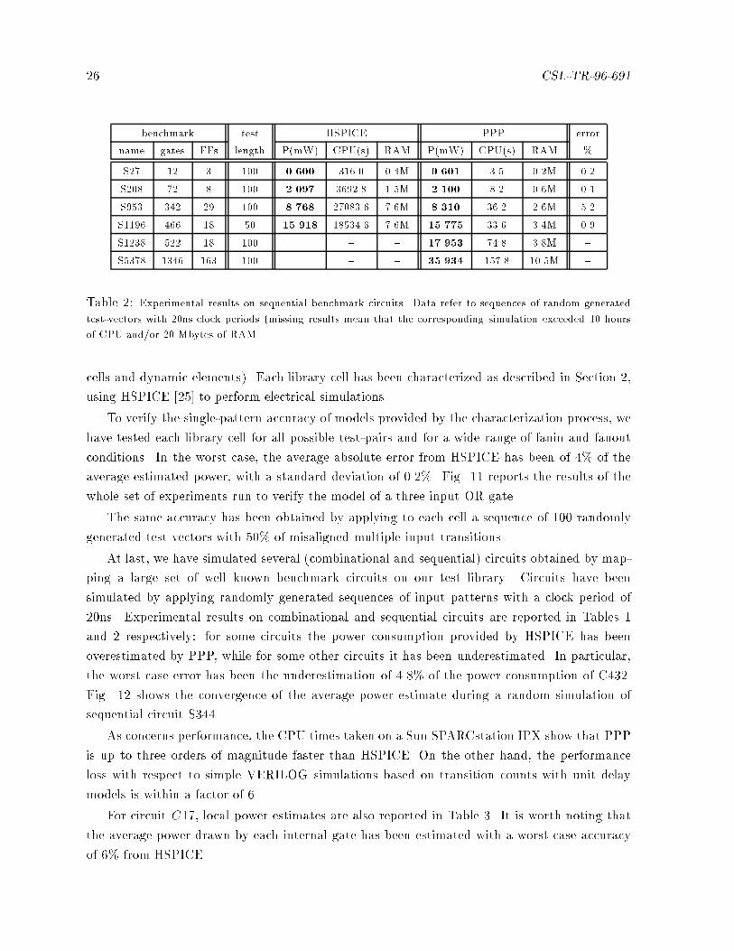
26 CSL-TR-96-691
benchmark test HSPICE PPP error
name gates FFs length P(mW) CPU(s) RAM P(mW) CPU(s) RAM %
S27 12 3 100 0.600 316.0 0.4M 0.601 3.5 0.2M 0.2
S208 72 8 100 2.097 3692.8 1.5M 2.100 8.2 0.6M 0.1
S953 342 29 100 8.768 27083.6 7.6M 8.310 36.2 2.6M 5.2
S1196 466 18 50 15.918 18534.6 7.6M 15.775 33.6 3.4M 0.9
S1238 522 18 100 { { { 17.953 74.8 3.8M {
S5378 1346 163 100 { { { 35.934 157.8 10.5M {
Table 2: Experimental results on sequential benchmark circuits. Data refer to sequences of random generated
test-vectors with 20ns clock periods (missing results mean that the corresponding simulation exceeded 10 hours
of CPU and/or 20 Mbytes of RAM.
cells and dynamic elements). Each library cell has been characterized as described in Section 2,
using HSPICE [25] to perform electrical simulations.
To verify the single-pattern accuracy of models provided by the characterization process, we
have tested each library cell for all possible test-pairs and for a wide range of fanin and fanout
conditions. In the worst case, the average absolute error from HSPICE has been of 4% of the
average estimated power, with a standard deviation of 0.2%. Fig. 11 reports the results of the
whole set of experiments run to verify the model of a three input OR gate.
The same accuracy has been obtained by applying to each cell a sequence of 100 randomly
generated test vectors with 50% of misaligned multiple input transitions.
At last, we have simulated several (combinational and sequential) circuits obtained by map-
ping a large set of well known benchmark circuits on our test library. Circuits have been
simulated by applying randomly generated sequences of input patterns with a clock period of
20ns. Experimental results on combinational and sequential circuits are reported in Tables 1
and 2 respectively: for some circuits the power consumption provided by HSPICE has been
overestimated by PPP, while for some other circuits it has been underestimated. In particular,
the worst case error has been the underestimation of 4.8% of the power consumption of C432.
Fig. 12 shows the convergence of the average power estimate during a random simulation of
sequential circuit S344.
As concerns performance, the CPU times taken on a Sun SPARCstation IPX show that PPP
is up to three orders of magnitude faster than HSPICE. On the other hand, the performance
loss with respect to simple VERILOG simulations based on transition counts with unit delay
models is within a factor of 6.
For circuit C17, local power estimates are also reported in Table 3. It is worth noting that
the average power drawn by each internal gate has been estimated with a worst case accuracy
of 6% from HSPICE.

Conclusions and Future Work 27
0 500 1000 1500 2000time (ns)
0
2000
4000
6000
pow
er (
uW)
Figure 12: Convergence of the average power estimation during a random simulation of circuit S208 with 100
test patterns. A 20ns clock period has been used.
8 Conclusions and Future Work
In this work we presented a cell characterization and logic simulation algorithm that reduces the
gap between the accuracy of electrical and logic-level power estimation for cell-based designs.
Statistical uncertainties on device characteristics or inaccuracies on wiring capacitance extraction
and modeling may lead to mismatches between circuit simulation and measured values that are
larger than the inaccuracy of our simulator. As a consequence, our simulation technique gives
the designer a level of con�dence on power dissipation estimates comparable to those attainable
with computationally expensive circuit simulation. The high local accuracy makes our tool a
valuable source of information for power optimization algorithms that operate locally within a
gate-level network.
Our technique achieves better accuracy than previously presented approaches and requires
storage of lookup tables with size similar to those required for logic simulation with accurate
delay. Important e�ects such as charge sharing, short circuit current, and misaligned multiple
input transitions are taken into account. Moreover, we use as simulation platform a well known
VERILOG simulator such as VERILOG-XL, making the interface with pre-existing design ows
and RTL simulation completely straightforward.
The customized Verilog simulator has been embedded in PPP, an integrated Web-based
environment for the simulation of low-power VLSI systems. We have described the architecture
and the implementation of PPP. We believe that PPP is an example of a new paradigm for
distributed network-based applications, where the connectivity o�ered by Internet is exploited
not only for retrieving information but also to dispatch and control execution.
On-going work is focused on integrating more advanced functionalities in PPP. New algo-
rithms for behavioral power estimation will be included in future versions of the tool. Moreover,

28 CSL-TR-96-691
Cell Power (mW) Error
# HSPICE PPP (mW) (%)
0 0.032 0.031 -0.001 3
1 0.038 0.037 -0.001 3
2 0.043 0.042 -0.001 2
3 0.156 0.154 -0.002 1
4 0.032 0.030 -0.002 6
5 0.134 0.138 +0.004 3
tot 0.435 0.432 -0.003 1
Table 3: Local power consumption of a NAND-only realization of benchmark circuit C17. Data refer to a
sequence of 100 random generated test vectors, with a 20ns clock period.
we are currently developing algorithms that will allow accurate estimation of current waveforms
at the logic level. Synthesis tools for low-power will be integrated in PPP as well. In summary,
the implementation of PPP demonstrates the feasibility of one key concept: a uniform user
interface for a heterogeneous set of EDA tools based on the WWW.
9 Acknowledgements
We would like to thank Michele Favalli at DEIS, University of Bologna, for many useful sugges-
tions.

29
References
[1] C. Huang, B. Zhang, et al., \The design and implementation of Powermill," in Proc. of IEEE Symp. on Low
Power Electronics, pp. 105{110, 1995.
[2] F. Najm, \A survey of power estimation techniques in VLSI circuits," IEEE Transaction on VLSI Systems,
vol. 2, no. 4, pp. 446{455, 1994.
[3] C. Y. Tsui, M. Pedram, and A. Despain, \E�cient Estimation of Dynamic Power Dissipation under a Real
Delay Model," in Proc. of IEEE Int.l Conf. On Computer Aided Design, pp. 224{228, 1993.
[4] R. Marculescu, D. Marculescu, and M. Pedram, \Logic level power estimation considering spatiotemporal
correlations," in Proc. of IEEE Int.l Conf. On Computer Design, pp. 294{299, 1994.
[5] D. Liu and C. Svensson, \Power consumption estimation in CMOS VLSI chips," IEEE J. of Solid State
Circuit, vol. 29, no. 6, pp. 663{670, 1994.
[6] P. Landman and J. Rabaey, \Architectural power analysis, the Dual Bit Type method," IEEE Transaction
on VLSI Systems, vol. 3, no. 2, pp. 173{187, 1995.
[7] R. S. Martin and J. Knight, \Power-Pro�ler: optimizing ASICs power consumption at the behavioral level,"
in Proc. of Design Automation Conf., pp. 42{47, 1995.
[8] B. J. George et al., \Power analysis and characterization for semi-custom desing," in Proc. of Int.l Workshop
on Low Power Design, pp. 215{218, 1994.
[9] J.-Y. Lin et al., \A cell-based power estimation in CMOS combinational circuits," in Proc. of IEEE Int.l
Conf. On Computer Aided Design, pp. 304{309, 1994.
[10] H. Sarin and A. McNelly, \A power modeling and characterization method for logic simulation," in Proc. of
IEEE Custom Integrated Circuits Conference, pp. 363{366, 1995.
[11] L. Benini, M. Favalli, and B. Ricc�o, \Analysis of hazard contribution to power dissipation in CMOS IC's,"
in Proc. of Int.l Workshop on Low Power Design, pp. 27{32, 1994.
[12] R. E. Bryant, \Graph-based algorithms for boolean function manipulation," IEEE Transaction on Comput-
ers, vol. 35, no. 8, pp. 677 { 691, 1986.
[13] N. Weste and K. Eshraghian, Principles of CMOS VLSI Design (Second Edition). Addison-Wesley, 1992.
[14] R. Bahar et al., \Algebraic decision diagrams and their applications," in Proc. of IEEE Int.l Conf. On
Computer Aided Design, pp. 188{191, 1993.
[15] T. J. Barnes et al., Electronic CAD frameworks. Kluwer Academic Publishers, 1992.
[16] A. Bededenfeld and R. Camposano, \Tool integration and construction using generated graph-based design
representation," in Proc. of Design Automation Conf., pp. 94{99, 1995.
[17] T. Berners-Lee et al., \The world-wide web," Communications of the ACM, vol. 37, no. 8, pp. 76 { 82, 1994.
[18] M. J. Silva and R. H. Katz, \The case for design using the World Wide Web," in Proc. of Design Automation
Conf., pp. 579{585, 1995.
[19] P. G. Ploger et al., \WWW Based structuring of codesigns," in Proc. of Int.l Symposium on System Synthesis,
pp. 138{143, 1995.
[20] E. Sentovich et al., \Sequential circuit design using synthesis and optimization," in Proc. of IEEE Int.l Conf.
On Computer Design, pp. 328{333, 1992.
[21] \HyperText Markup Language (HTML)," Working and background materials, http://www.w3.org/
hypertext/WWW/MarkUp/MarkUp.html.

30 CSL-TR-96-691
[22] Sun Microsystems, \The JAVA language environment: a white paper," http://java.sun.com/whitePaper/
java-whitepaper-1.html.
[23] J. K. Ousterhout, Tcl and the Tk toolkit. Addison-Wesley, 1994.
[24] T. Burd, \Current Estimation in MOS IC Logic Circuits," in M. S. Report UC Berkeley, UCB/ERLM94/89.
[25] HSPICE User's Manual. Meta-Software Inc., Campbell-CA.