Advanced CMOS Device Physics :...
24
Raphaël CLERC Associate Professor at Grenoble INP University Researcher at IMEP [email protected] Advanced CMOS Device Physics : Introduction
Transcript of Advanced CMOS Device Physics :...

Raphaël CLERC
Associate Professor at Grenoble INP University
Researcher at IMEP
Advanced CMOS Device Physics :Introduction

Objectives :
Outline of the lectures :
INTRODUCTION :
an overview of Nanoelectronics
an overview of MOSFET device engineering issues
PART 1 : review of long channel device physics
PART 2 : advanced features (short channel effects and velocity saturation)
• Give an overview of the advanced MOSFET device physics issues
• Address in more details some specific aspects, including scaling
• Learn some analytical models useful to understand and analyze device performances

INTRODUCTION : an overview of Nanoelectronics
• Electronics History
• Overview in research in Nanoelectronics (logic application)
• Main Players in Europe

Electronics History
Transistor inventors (1948)
BRATTAINExperimentalist
BARDEENTheorician
SHOCKLEYTheorician
1926 : First transistor Patent (J. E. Lilienfeld)
1948 : Bipolar Transistor (Schockley, Brattain and Bardeen)
1954 : First Silicon Transistor (TI)
1958 : Integrated Circuit (J. Kilby)
1960 : MOS transistor (M. Atalla, D. Kahng)
1971 : Microprocessor (INTEL)
IC inventor J. Kilby (1958)First IC (1958)
First Transisor (1948)

An overview of Resarch
in Nanoelectronics (Logic)
Single electron devices, Molecular
devices,
Ferromagnetic logic devices, Spintronics
MEMS
Plastic Electronics
New Material for Power Electronics : SiC, GaN
SOI devicesFinFet devices
MultiGate Devices
High Mobility Materials Ge, III V for ultra scaled devices :
Low dimensional structures including carbon nanotube
FETs, nanowire FETs, nanoribbon graphene.
INTEL's Trigate FET
(VLSI'06)
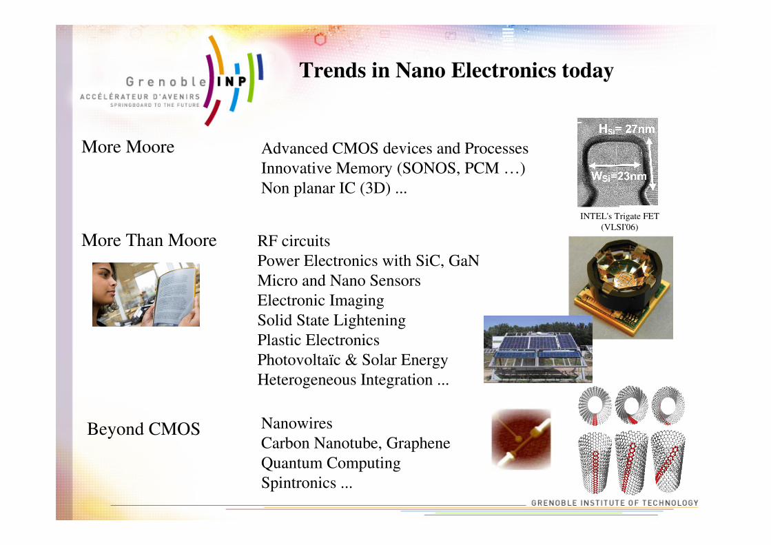
Beyond CMOS Nanowires
Carbon Nanotube, Graphene
Quantum Computing
Spintronics ...
More Moore Advanced CMOS devices and Processes
Innovative Memory (SONOS, PCM …)
Non planar IC (3D) ...
INTEL's Trigate FET
(VLSI'06)
More Than Moore RF circuits
Power Electronics with SiC, GaN
Micro and Nano Sensors
Electronic Imaging
Solid State Lightening
Plastic Electronics
Photovoltaïc & Solar Energy
Heterogeneous Integration ...
Trends in Nano Electronics today
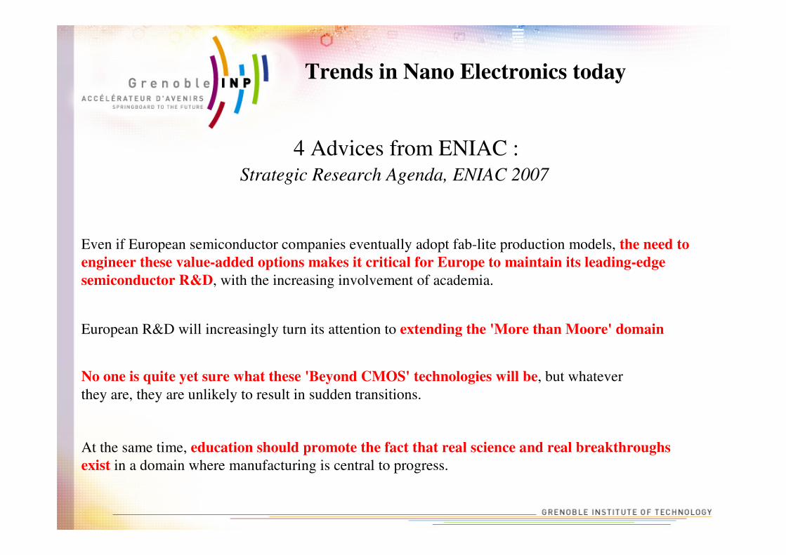
Even if European semiconductor companies eventually adopt fab-lite production models, the need to
engineer these value-added options makes it critical for Europe to maintain its leading-edge
semiconductor R&D, with the increasing involvement of academia.
European R&D will increasingly turn its attention to extending the 'More than Moore' domain
At the same time, education should promote the fact that real science and real breakthroughs
exist in a domain where manufacturing is central to progress.
Trends in Nano Electronics today
4 Advices from ENIAC :
No one is quite yet sure what these 'Beyond CMOS' technologies will be, but whatever
they are, they are unlikely to result in sudden transitions.
Strategic Research Agenda, ENIAC 2007

Main Players in
Semiconductor Industry
In Europe :
• ST
• Infineon
(in alliance with IBM)
Research :
LETI (Minatec)
IMEC
INTRODUCTION : an overview of MOSFET device engineering issues
• The very basic of MOSFET device physics (recap) :
Operation principle, figure of merits, High Performance and Low Power MOSFET, Scaling
• Overview of challenges in MOSFET Physics and Technology today :
Issues of in conventional bulk devices, solutions under investigation
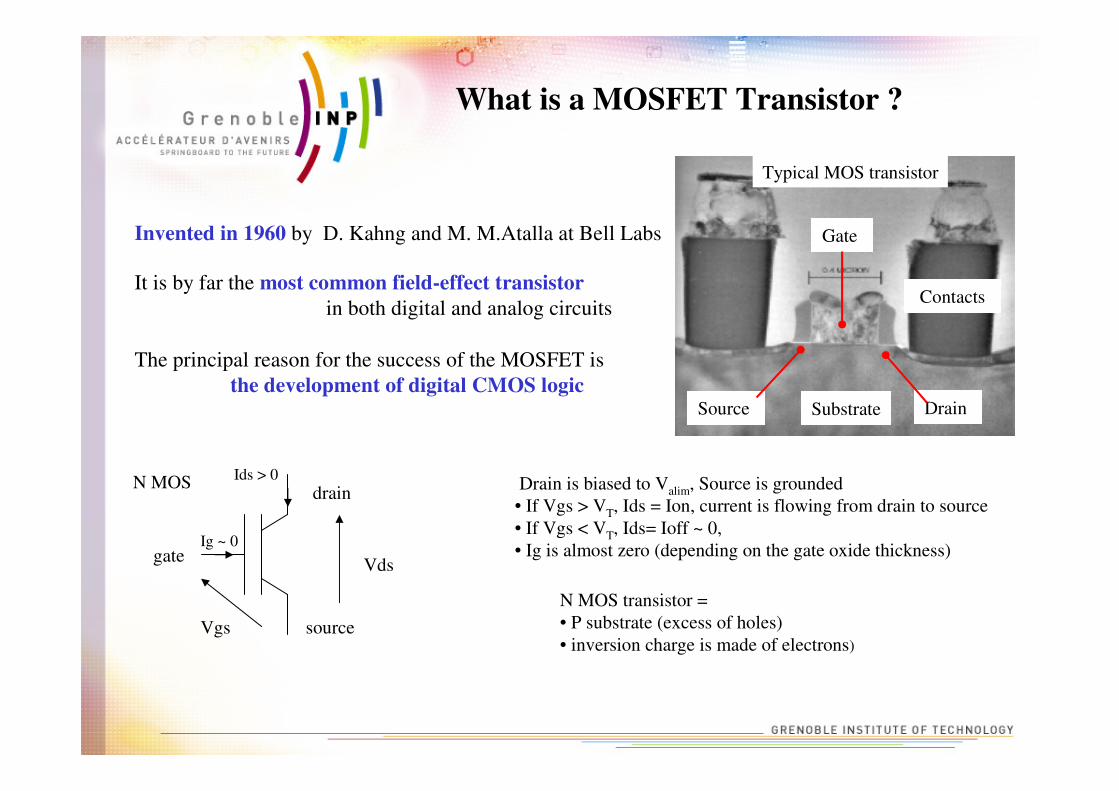
What is a MOSFET Transistor ?
source
drain
gate
Vgs
Vds
Ids > 0
Ig ~ 0
Drain is biased to Valim, Source is grounded
• If Vgs > VT, Ids = Ion, current is flowing from drain to source
• If Vgs < VT, Ids= Ioff ~ 0,
• Ig is almost zero (depending on the gate oxide thickness)
N MOS transistor =
• P substrate (excess of holes)
• inversion charge is made of electrons)
N MOS
Gate
Source Drain
Typical MOS transistor
Contacts
Substrate
It is by far the most common field-effect transistor
in both digital and analog circuits
Invented in 1960 by D. Kahng and M. M.Atalla at Bell Labs
The principal reason for the success of the MOSFET is
the development of digital CMOS logic

Main MOSFET figures of merit
An important calculated output parameter is the intrinsic
MOSFET delay, τ = CV/I, where C is the total gate capacitance (including parasitic gate overlap and fringing capacitance) per micron transistor width, V is the power supply voltage (Vdd), and Ion is the saturation drive current per micron transistor width.
τ is a good metric for the intrinsic MOSFET delay, and hence 1/ ττττ is a good metric for the maximum intrinsic MOSFET switching frequency.
intrinsic MOSFET delay :on
dd
I
V C=τ
Vds =Vdd >> kT / e
Gate Voltage Vgs (V)
Cu
rren
t Id
s(i
n L
OG
sca
le)
(µA
/µm
)
Threshold voltage VT
SubthresholdSlope
Vds << kT / e
Ion
Ioff
Vdd0( THE INTERNATIONAL TECHNOLOGY ROADMAP
FOR SEMICONDUCTORS: 2007 )
(For digital CMOS application)
ds gs dd ds dd ds gs dd ds dd
eff
I (V V / 2, V V ) I (V V ,V V / 2)I
2
= = + = =
=A more accurate criteria :
"The effective drive current in CMOS inverters",
M. H. Na et al., proc. IEDM 2002.
on ds gs dd ds ddI I (V V , V V )= = =

Particular role of VT in Ion / Ioff trade off
Gate Voltage Vgs (V)
An increase in threshold voltage VT results in :
Assuming a constant subthreshold slope …
An decreaseof Ioff
An decrease of Ion
Cu
rren
t I d
s(i
n L
OG
sca
le)
(µA
/µm
)

High-performance logic refers to chips of high complexity, high performance, and high power dissipation,
such as microprocessor unit (MPU) chips for desktop PCs, servers, etc.
For the high-performance logic, the driver is the MOSFET intrinsic performance metric, 1/τ. Specifically, the target is
an average 17% per year increase in 1/τ, which matches the historic rate of improvement in device performance.
Meeting this target is an important enabler for the desired rate of improvement in the chip clock speed.
The transistors for high-performance ICs have both the highest performance and the highest leakage current of all, and hence the physical gate length and all the other transistor dimensions are most rapidly scaled for high performance logic.
Low-power logic refers to chips for mobile systems, where the allowable power dissipation and hence the
allowable leakage currents are limited by battery life.
There are two major categories within low-power, low operating power (LOP) and low standby power (LSTP) logic.
LOP chips are typically for relatively high-performance mobile applications, such as notebook computers, where the battery is likely to be high capacity and the focus is on reduced operating (i.e., dynamic) power dissipation.
LSTP chips are typically for lower performance, lower cost consumer type applications, such as consumer cellular telephones, with lower battery capacity and an emphasis on the lowest possible static power dissipation, i.e., the lowest possible leakage current.
The LSTP and LOP curves for 1/τ scaling show similar effects, although the overall performance increase is ~13-
14%/year for these.
Concepts of High Performance
and Low power MOSFETs
MOSFET Scaling
2007 2010 2013 2016 20190
10
20
30
65 nm node
45 nm node
32 nm node
22 nm node
16 nm node
Year
Ch
ann
el L
eng
th(n
m)
11 Å
6.5 Å
5 ÅEOT
EOT =
Equivalent Oxide
Thickness (nm)
High Performance
scaling
( THE INTERNATIONAL TECHNOLOGY ROADMAP FOR SEMICONDUCTORS: 2007 )
Why scaling ?
to pack more and more devices in a given chip area.
(i.e. more functionality in the same area)
reduction of the chip cost (at same functionality)
smaller transistors are expected to switch faster.
The main device dimensions are the transistor length, width, and the oxide thickness,
each (used to) scale with a factor of 0.7 per node.
High Performance

The End of « Happy Scaling »
30 40 50 60 70500
1000
1500
2000
Technological node (nm)
Ion
curr
ent
(µA
/µm
)
nMOS
pMOS
INTEL HP
20 30 40 50 60 7020
40
60
Technological node (nm)
Ph
ysi
cal
gat
e le
ngth
(n
m) INTEL HP 65 nm
45 nm
32 nm
• Performances keep increasing according Moore Law
• However, transistor dimension remains approximately constant
• The cause of performance improvement is no longer simple scaling, but the introduction of booster
( strain, metal gate …)
Scaling at constant voltage does not sufficiently improve performance

High K materials (HfO2?)• low level of tunnel current
• but … low quality interface
• reduction of mobility
• reduce polydepletion
• mandatory for High K materials
• but …VFB
Series resistance :Gate and source and drain silicidation
Strained silicon channel :• improve mobility on long channel
• may ? improve performance
on short channels
Metallic Gate :
Major problem :• control of short channel effects require high doping level
• high doping level kill mobility
Main issues in conventional Bulk MOSFET
Doping fluctuations :• small numbers of doping atoms
• induce VT and Ion Ioff fluctuations
With scaling of planar bulk MOSFETs, the channel doping will need to be increased to undesirably high levels in order to gain adequate control of short-channel effects and to set the threshold voltage properly. As a result of the high channel doping, the mobility of holes and electrons will be reduced.( THE INTERNATIONAL TECHNOLOGY ROADMAP FOR
SEMICONDUCTORS: 2005 )

Technology Today
INTEL 32 nm High Performance Technology (IEDM 2009)
• BULK Technology
• Gate Length L = 30 nm
• EOT 0.9 nm
• Dual High K Metal Gates
Strain Boosters :
PMOS : embedded Source and Drain SiGe + nitride stress capping layer
NMOS : Stress Memorization Techniques + nitride stress capping layer
NMOS Ion = 1620 µA / µm
PMOS Ion = 1370 µA / µm
Vdd = 1V and Ioff = 100 nA/µm
INTEL 32 nm (IEDM 2009)
INTEL 45 nm (VLSI 2008)

Better than bulk CMOS ? :
Fully Depleted MOSFETs
Fully depleted
SOI devices
Main advantage :• control of SCE and DIBL is achieved by thin body thickness
Due to the challenges with scaling planar bulk MOSFETs, advanced devices such as ultra-thin body fully depleted SOI
MOSFETs and multiple-gate MOSFETs (e.g., FinFETs) are expected to be eventually implemented. Since such devices will
typically have lightly doped channels and the threshold voltage will be controlled by the metal gate electrode’s work function, the challenges associated with high channel doping and stochastic dopant variation in planar bulk MOSFETs will be avoided,
but numerous new challenges are expected. Amongst the most critical of such challenges will be controlling the body
thickness and its variability for these ultra-thin structures, and setting the metal gate electrode work function to its desired
value. As with the planar bulk MOSFET, it will be highly challenging to reduce the parasitic series source/drain resistance
(Rsd) to tolerable values, but here the ultra-thin body is an added difficulty.( THE INTERNATIONAL TECHNOLOGY ROADMAP FOR SEMICONDUCTORS: 2005 )
Body

Double gate Transistors
DG SOI or SON
FIN FET
Devices
Gate All- Around
(GAA) Devices
Better than bulk CMOS ? :
Multigate devices
Main advantage :• control of SCE and DIBL is achieved by thin body thickness and the number of gates

0
0.2
0.4
0.6
0.8
1
20 40 60 80
Channel Length (nm)
Sili
con thic
kness t
si/ L r
atio
Double Gate
Single Gate
Quadruple Gate
Criteria : 6 lc > L > 8 lc
Better than bulk CMOS ? :
Multigate devices
Main advantage :• control of SCE and DIBL is achieved by thin body thickness and the number of gates

1 22 a µ /µ + bR =
P
0 0.2 0.4 0.6 0.8 10
1
2
3
Trigate (a = b)
a /P =1 / 4
a / P = 1
a / P = 2
Curr
ent (n
orm
aliz
ed to S
G)
Ratio Base / Pitch (b / P)
µ1 / µ2 = 0.5
W ’
Section :
Si Si
b
a
P insulator
one fingerGate
Better than bulk CMOS ? :
Multigate devices
Main issue: Multi fingers is hard to scale

Better than bulk CMOS ? :
Multigate devices
« World's First Demonstration of 22nm 3-D Tri-Gate Transistors »
« Intel putting fins on at 22 nm »Don Scansen
5/4/2011 12:39 PM EDT

Devices in the future
according the ITRS

Conclusions :
• MOSFETs factor of merits : Ion, Ioff, VT, S how to control them ?
• What are the « short channel » effects ?
Why does the control of short channel effect require to highly dope the channel in Bulk MOSFET device ?
• What are the advantages of Fully Depleted MOSFET and Multigate MOSFET ?
• What are quantum effects ?
These lectures should answer the following questions :