ESD Protection Device Simulation and Design - Silvaco · PDF fileESD Protection Device...
26
ESD Protection Device Simulation and Design
Transcript of ESD Protection Device Simulation and Design - Silvaco · PDF fileESD Protection Device...
ESD Protection Device Simulation and Design
ESD Protection Device Simulation and Design
• Electrostatic Discharge (ESD) is one of the major reliability issues in Integrated Circuits today
• ESD is a high current (1A) short duration (1ns to 100ns) event • Simulation gives physical insight into what mechanisms cause ESD
destruction and how device designs can be altered to be more resistant to ESD
• When modeling electrothermal interactions in semiconductor devices experiencing ESD pulses time–dependency and lattice heating must be included
• Real test conditions require that the device and its interaction with an external circuit are both simulated
Introduction
- 2 -
ESD Protection Device Simulation and Design
• Q1: Which Simulation Tools Are Used For ESD Related Problems?
• Q2: How are Silvaco Tools used for ESD Simulation?
Electrostatic Discharge (ESD) Simulation
- 3 -

ESD Protection Device Simulation and Design
• Atlas/Giga solves self-consistently the drift-diffusion semiconductor equations and the heat flow equation in the semiconductor and the heat sinks • Self-consistent solution of the heat flow equation using Wachutka’s thermodynamically
rigorous model which includes all thermal sources (Joule, Thomson and Recombination Heat)
• Dependencies of all electrical and thermal material parameters on the local lattice temperature (mobility, impact ionization, etc.)
• Arbitrary thermal boundary conditions, including thermal resistors and heat sinks, are allowed
• DC and transient analysis
Giga- Electrothermal Effects in Semiconductors
- 4 -
ESD Protection Device Simulation and Design
• Atlas/Giga/MixedMode solves both the embedded physically based Atlas devices and the connected spice circuit elements, simultaneously and self-consistently to provide a complete circuit solution to ESD event. • Links Atlas devices to a SPICE type circuit simulator • Multiple Atlas devices with independent models may be included in a single circuit • The SPICE input language is used for circuit specification • The usual SPICE primitives are available, and most commercially developed SPICE
models are supported • DC and transient analysis
MixedMode- Device-Circuit Interactions
- 5 -
ESD Protection Device Simulation and Design
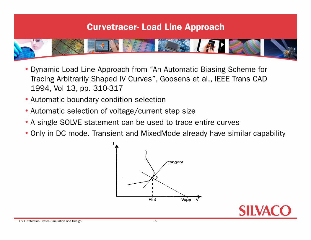
• Dynamic Load Line Approach from “An Automatic Biasing Scheme for Tracing Arbitrarily Shaped IV Curves”, Goosens et al., IEEE Trans CAD 1994, Vol 13, pp. 310-317
• Automatic boundary condition selection • Automatic selection of voltage/current step size • A single SOLVE statement can be used to trace entire curves • Only in DC mode. Transient and MixedMode already have similar capability
Curvetracer- Load Line Approach
- 6 -
ESD Protection Device Simulation and Design
• Atlas supports different arithmetic precision. Supported precision levels include:
Precision (bits): 64 80 128 160 256
• For well-converged solutions, run-time increases with precision. The increase is especially significant at the highest precision levels. On the other hand, certain problems that have difficulty converging at the lower precision levels are likely to run faster if the precision level is increased
Extended Precision Mode
- 7 -
ESD Protection Device Simulation and Design
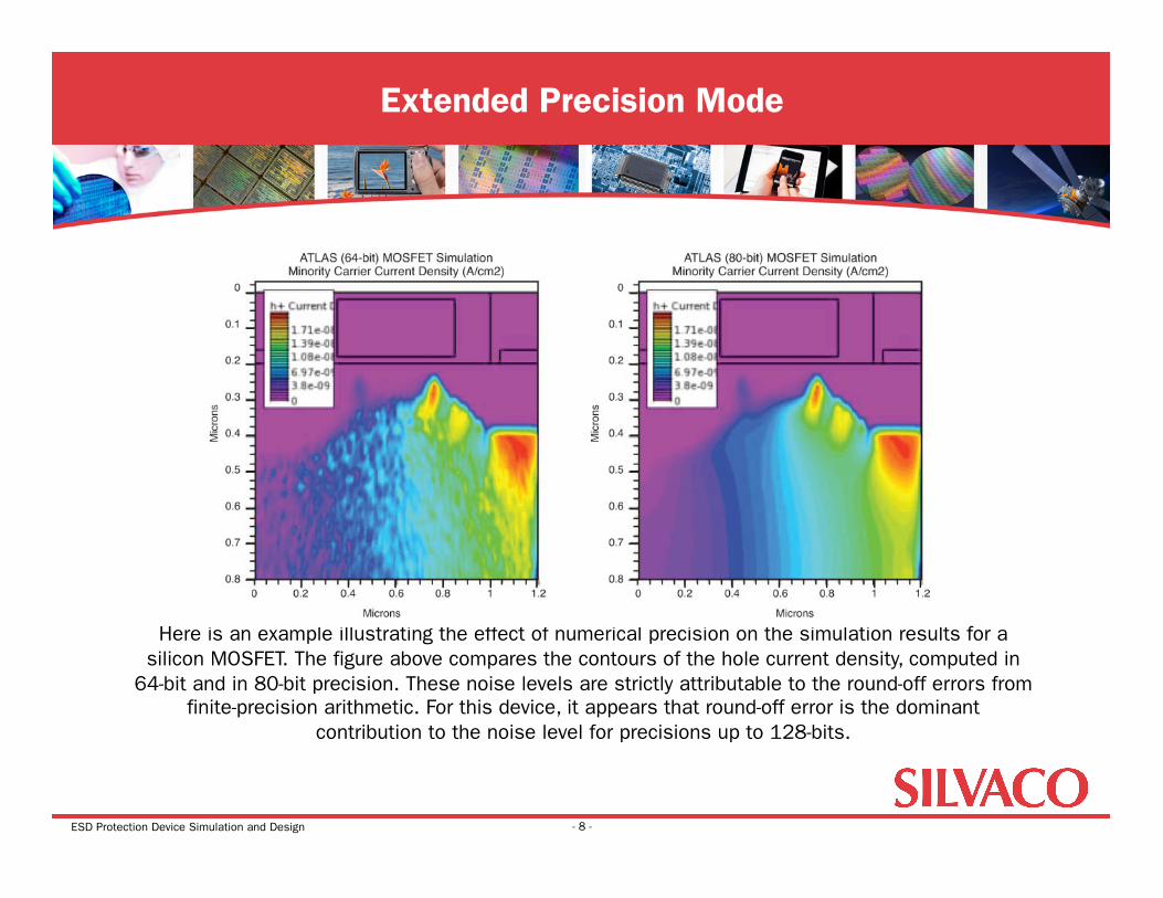
Here is an example illustrating the effect of numerical precision on the simulation results for a silicon MOSFET. The figure above compares the contours of the hole current density, computed in
64-bit and in 80-bit precision. These noise levels are strictly attributable to the round-off errors from finite-precision arithmetic. For this device, it appears that round-off error is the dominant
contribution to the noise level for precisions up to 128-bits.
Extended Precision Mode
- 8 -
ESD Protection Device Simulation and Design
• Silvaco and TMA TCAD software share a common legacy from Stanford University
• Athena is T-Supreme4™ compatible • Atlas is MEDICI™ compatible • This compatibility allows:
• Direct loading of input deck syntax • Support for the same physical models • Use of the same legacy material parameters
• Direct loading of TMA TIF format structure files • Sharing of users’ existing calibration coefficients
• TMA Users can migrate to Silvaco software easily • T-Supreme4 and MEDICI are trademarks of Synopsis Inc
Comprehensive TMA Compatibility
- 9 -
ESD Protection Device Simulation and Design
• Atlas Simulation Results • Silicon Controlled Rectifier (SCR) Latch-up
• Atlas/Giga Simulation Results • CMOS Protection Device Under HBM Test • MOS Second Breakdown
• Atlas/Giga/MixedMode Simulation Results • CMOS Protection Device Under CDM Test
• SmartSpice Simulation Results • CMOS Protection Device Under HBM Test
Typical Application Examples
- 10 -
ESD Protection Device Simulation and Design
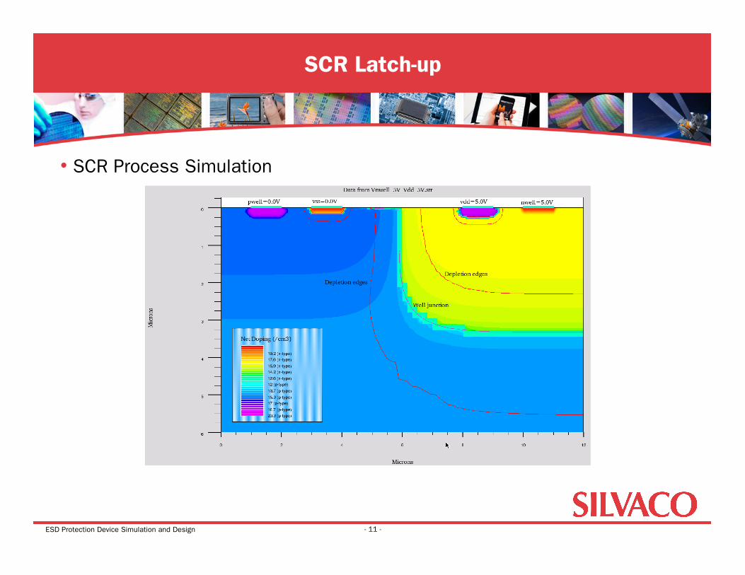
• SCR Process Simulation
SCR Latch-up
- 11 -

ESD Protection Device Simulation and Design
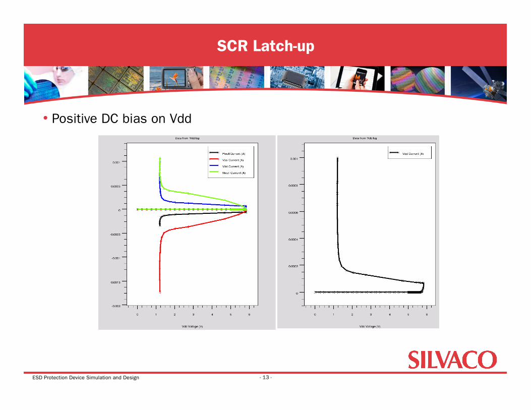
• DC Latch-up Simulation Step 1. Bias Vdd and Nwell to 5V 2. Apply positive bias ramp to Vdd, trace curve until Idd=1mA/um 3. Apply negative bias ramp to Vss, trace curve until Iss=1mA/um 4. Analyze curve to measure trigger voltage and holding current
SCR Latch-up
- 12 -
ESD Protection Device Simulation and Design
• Positive DC bias on Vdd
SCR Latch-up
- 13 -
ESD Protection Device Simulation and Design
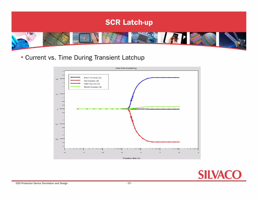
• Transient Device Simulation Setup 1. Bias Vdd and Nwell to 5V 2. Apply -1V pulse to Vss for several nanoseconds 3. Return Vss to zero continue simulation for 1us 4. Analyze current-time plot to analyze trigger point
SCR Latch-up
- 14 -
ESD Protection Device Simulation and Design
• Current vs. Time During Transient Latchup
SCR Latch-up
- 15 -
ESD Protection Device Simulation and Design
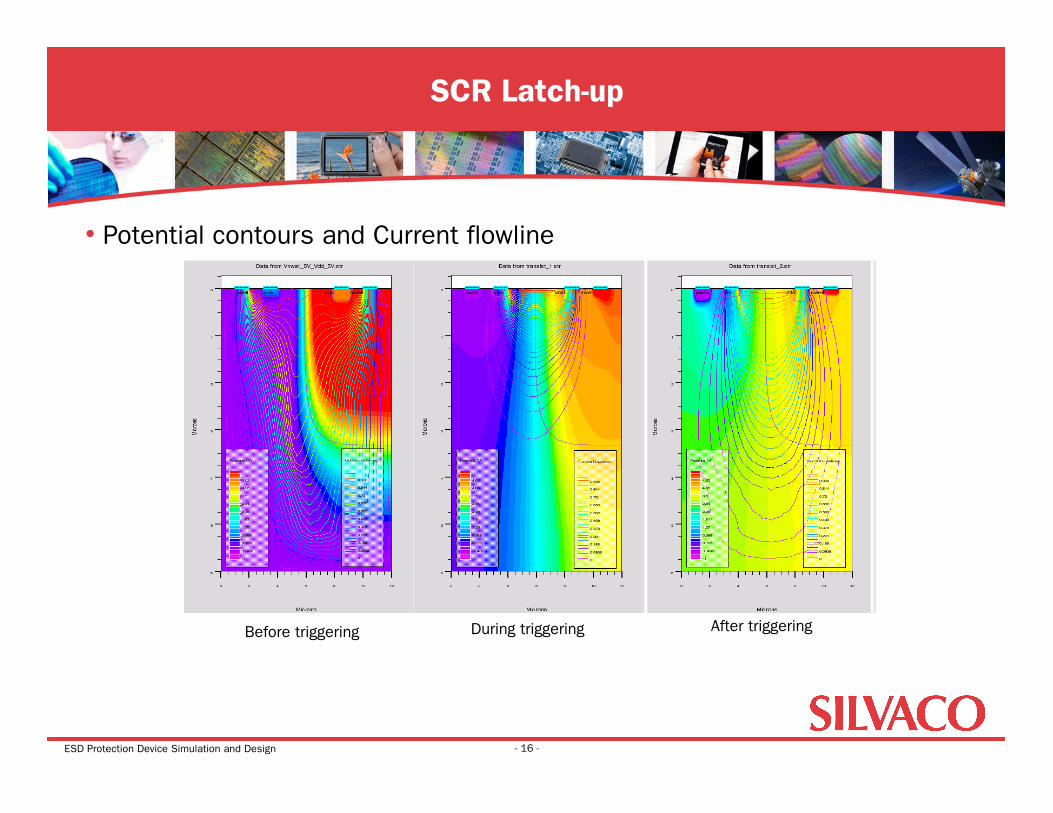
• Potential contours and Current flowline
SCR Latch-up
- 16 -
Before triggering During triggering After triggering
ESD Protection Device Simulation and Design
• HBM model consists of a 10ns linear current ramp followed by an exponential current drop with a time constant of 150ns
• For realistic simulation it is necessary to model the self-heating at high current levels • The local heating has to be combined with temperature dependent models for mobility,
recombination and impact ionization. • The combination of the complex transient pulse and advanced models means that ESD
pulse simulations are computationally intensive
CMOS Protection Device Under HBM Test
- 17 -
ESD Protection Device Simulation and Design
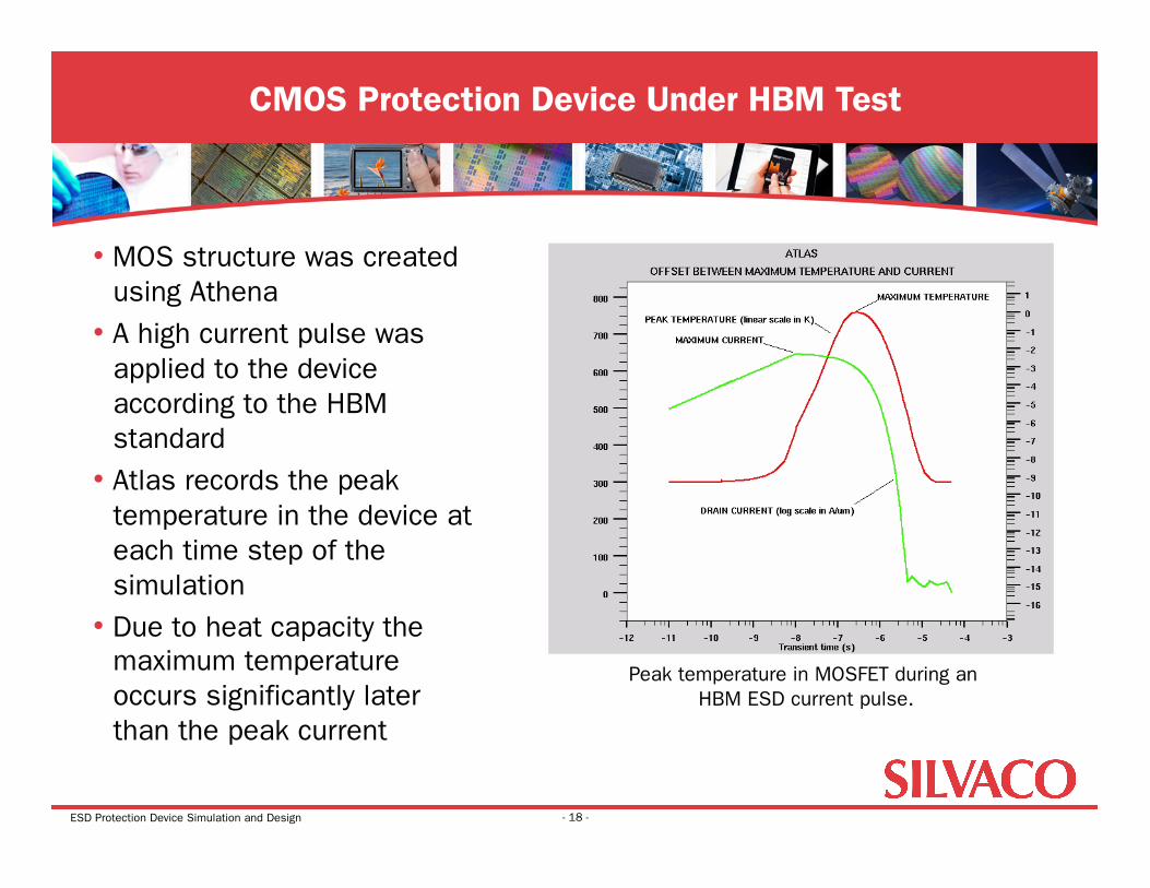
• MOS structure was created using Athena
• A high current pulse was applied to the device according to the HBM standard
• Atlas records the peak temperature in the device at each time step of the simulation
• Due to heat capacity the maximum temperature occurs significantly later than the peak current
CMOS Protection Device Under HBM Test
- 18 -
Peak temperature in MOSFET during an HBM ESD current pulse.
ESD Protection Device Simulation and Design
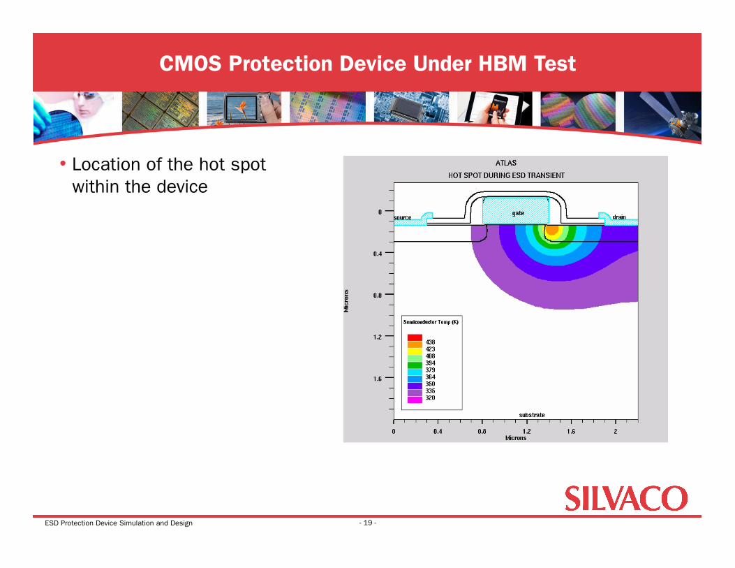
• Location of the hot spot within the device
CMOS Protection Device Under HBM Test
- 19 -
ESD Protection Device Simulation and Design
• Typical applications of ESD simulations are to examine the ESD performance of different drain engineering designs, to examine the position of the drain contact with respect to the hot spot and to observe the peak electric field across the gate oxide
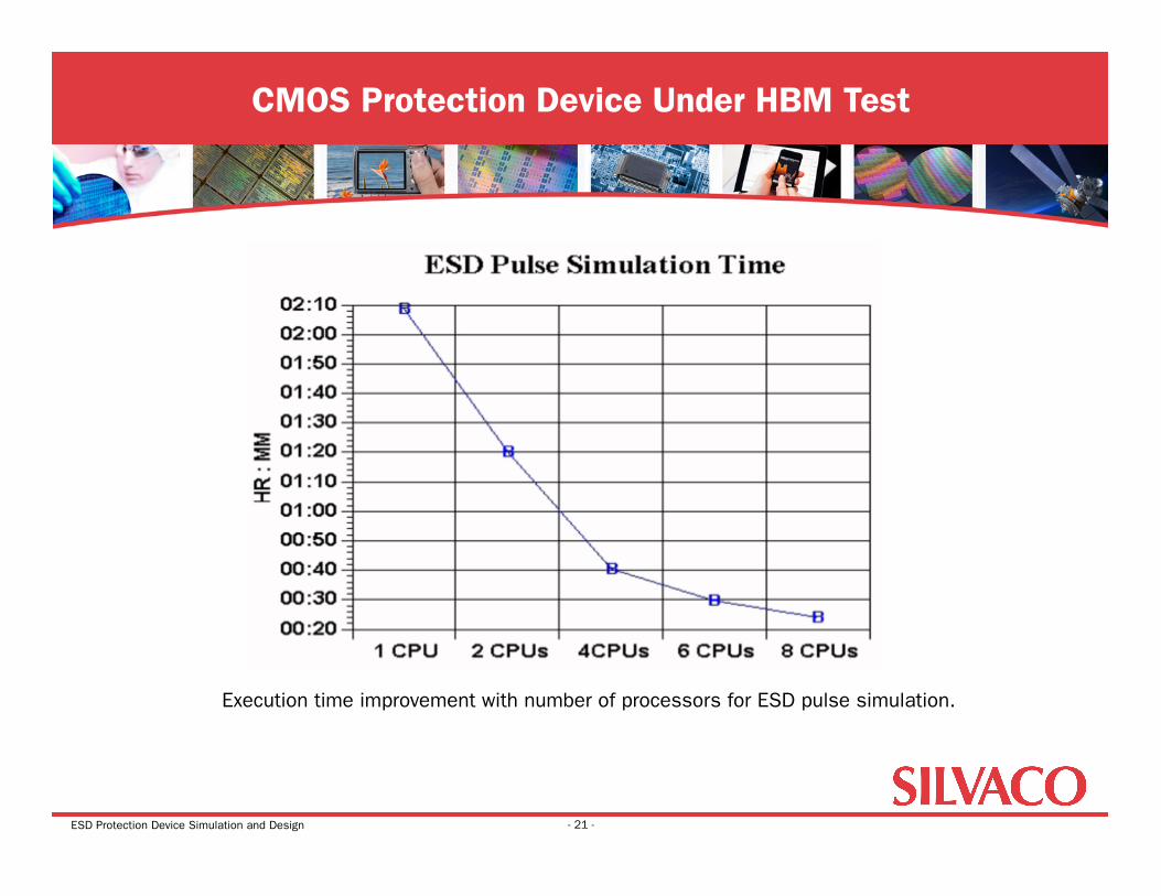
• This simulation was executed using parallel Atlas with increasing number of processors • The reduction in execution time vs the number of processors is shown in the following
slides • A high efficiency is seen even though the mesh used is not large
CMOS Protection Device Under HBM Test
- 20 -
ESD Protection Device Simulation and Design
CMOS Protection Device Under HBM Test
- 21 -
Execution time improvement with number of processors for ESD pulse simulation.
ESD Protection Device Simulation and Design
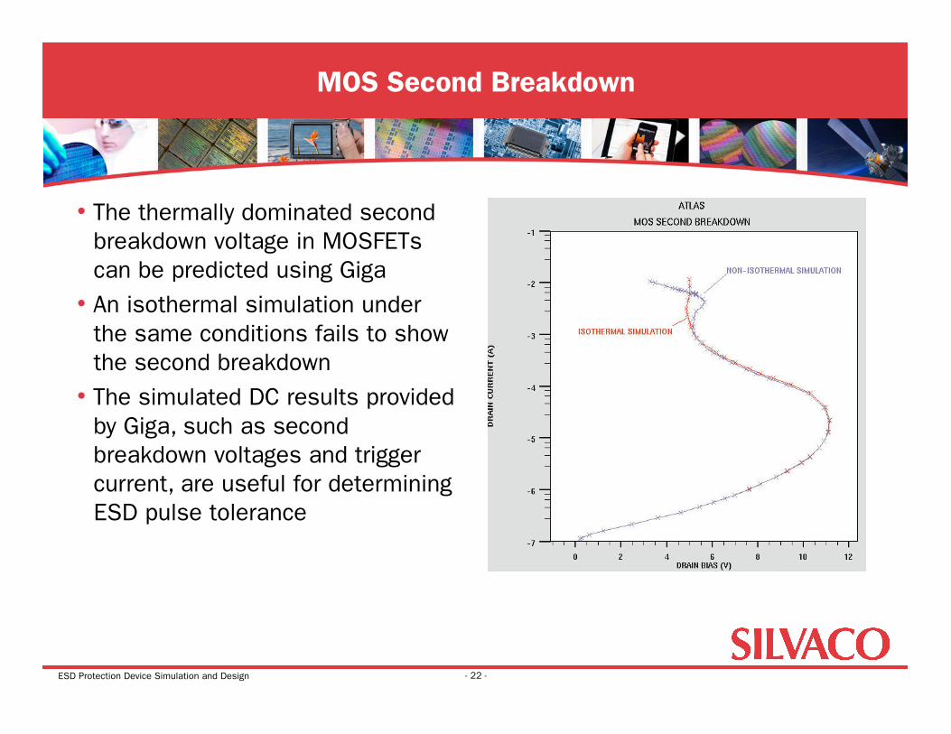
• The thermally dominated second breakdown voltage in MOSFETs can be predicted using Giga
• An isothermal simulation under the same conditions fails to show the second breakdown
• The simulated DC results provided by Giga, such as second breakdown voltages and trigger current, are useful for determining ESD pulse tolerance
MOS Second Breakdown
- 22 -
ESD Protection Device Simulation and Design
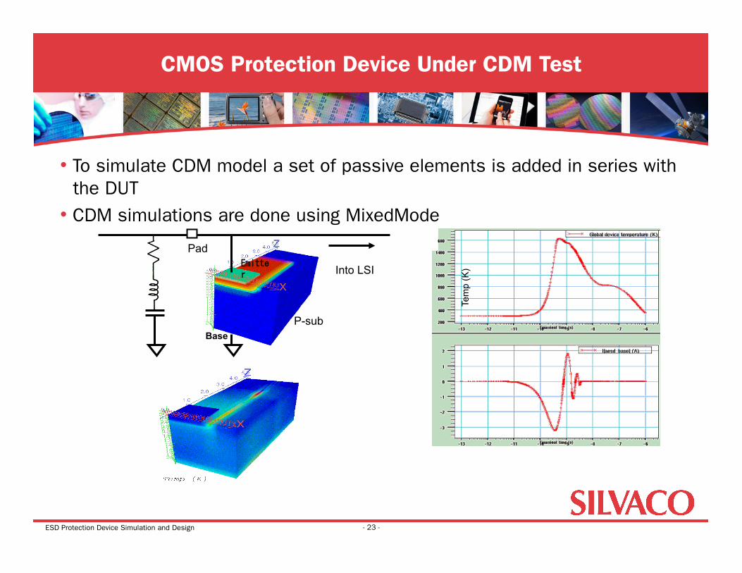
• To simulate CDM model a set of passive elements is added in series with the DUT
• CDM simulations are done using MixedMode
CMOS Protection Device Under CDM Test
- 23 -
Into LSI
Pad Emitter
Base P-sub
Tem
p (K
)
ESD Protection Device Simulation and Design
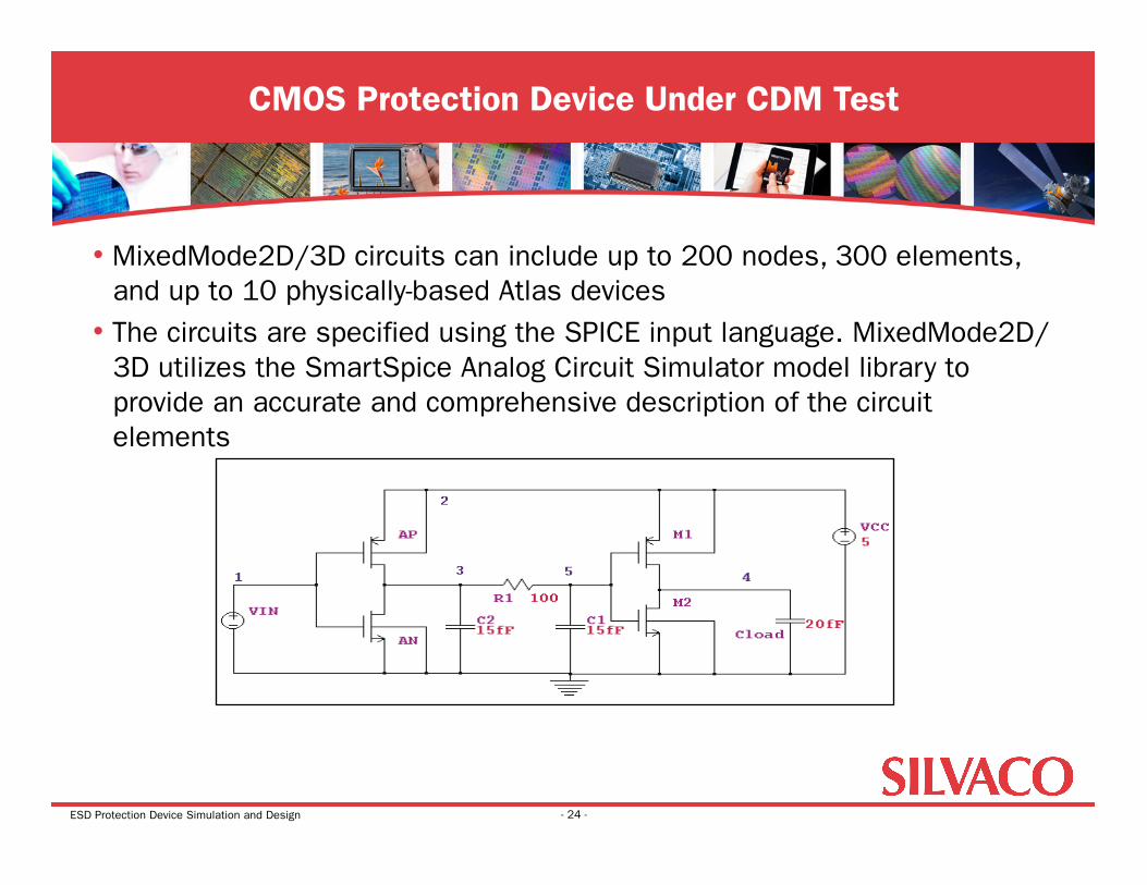
• MixedMode2D/3D circuits can include up to 200 nodes, 300 elements, and up to 10 physically-based Atlas devices
• The circuits are specified using the SPICE input language. MixedMode2D/3D utilizes the SmartSpice Analog Circuit Simulator model library to provide an accurate and comprehensive description of the circuit elements
CMOS Protection Device Under CDM Test
- 24 -
ESD Protection Device Simulation and Design
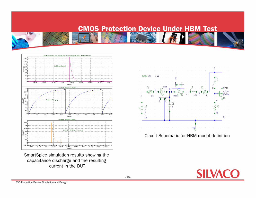
CMOS Protection Device Under HBM Test
Circuit Schematic for HBM model definition
SmartSpice simulation results showing the capacitance discharge and the resulting
current in the DUT
- 25 -
ESD Protection Device Simulation and Design
• ESD is a real threat to IC reliability • Treating ESD-related problem is very challenging • The use of TCAD helps to understand and optimize ESD design protection
and therefore reducing IC development costs and time • However specific device physics and numerics are needed to obtain
reliable results • Automation and Optimization can be performed using Virtual Wafer Fab
Conclusion
- 26 -