ACPL-339J Dual-Output Gate Drive Optocoupler Interface ... · cross conduction at external MOSFET...
23
CAUTION: It is advised that normal static precautions be taken in handling and assembly of this component to prevent damage and/or degradation which may be induced by ESD. Description The ACPL-339J is an advanced 1.0 A dual-output, easy-to- use, intelligent IGBT and Power MOSFET gate drive opto- coupler interface. Uniquely designed to support MOSFET buffer of various current ratings, the ACPL-339J makes it easier for system engineers to support different system power ratings using one hardware platform by inter- changing the MOSFET buffers and power IGBT/MOSFET switches. These changes can be made without redesign- ing the critical circuit isolation and short-circuit protec- tion. This concept maximizes gate drive design scalabil- ity for motor control and power conversion applications ranging from low to high power ratings. The ACPL-339J contains a AlGaAs LED. The LED is optically coupled to an integrated circuit with two power output stages with active timing control to prevent cross conduction at external MOSFET buffer. It is also integrated with features such as V CE detection, under voltage lockout (UVLO), “soft” IGBT turn-off, and isolated open collector fault feedback to provide maximum design flexibility and circuit protection. The ACPL-339J has an insulation voltage of V IORM = 1414 V peak in IEC/EN/DIN EN 60747-5-5. Functional Diagram Features • Dual output drive for external NMOS and PMOS buffer • 1.0 A minimum peak output current • Active timing control to prevent cross conduction in MOSFET buffer • IGBT desaturation detection • Isolated DESAT and UVLO fault feedback • Configurable “Soft” shutdown during fault • Under Voltage Lock-Out Protection (UVLO) with Hysteresis for positive and negative power supply • 300 ns maximum propagation delay over temperature range. • 6.0 mA to 10.0 mA Low LED input current • 25 kV/µs Minimum Common Mode Rejection (CMR) at V CM = 1500 V • Wide Operating V CC Range: 15 to 30 Volts • Industrial temperature range: -40° C to 105° C • SO-16 package • Safety Approval Pending – UL Recognized 5000 V RMS for 1 min. – CSA – IEC/EN/DIN EN 60747-5-5 V IORM = 1414 V peak Applications • IGBT/Power MOSFET gate drive Interface • AC and brushless DC motor drives • Renewable energy inverters • Industrial Inverters • Switching power supplies 13 SHIELD SHIELD D R I V E R DESAT V CC2 V OUTP V EE V CC1 V GND1 FAULT ANODE CATHODE V GMOS 3 2, 4 6 7 5, 8 12 16 15 14 UVLO_P LED1 LED2 V E V OUTN 11 9 UVLO_N DESAT Drive Logic & Overlap Protection ACPL-339J Dual-Output Gate Drive Optocoupler Interface with Integrated (V CE ) DESAT Detection, FAULT and UVLO Status Feedback Data Sheet
Transcript of ACPL-339J Dual-Output Gate Drive Optocoupler Interface ... · cross conduction at external MOSFET...

CAUTION: It is advised that normal static precautions be taken in handling and assembly of this component to prevent damage and/or degradation which may be induced by ESD.
DescriptionThe ACPL-339J is an advanced 1.0 A dual-output, easy-to-use, intelligent IGBT and Power MOSFET gate drive opto-coupler interface. Uniquely designed to support MOSFET buffer of various current ratings, the ACPL-339J makes it easier for system engineers to support different system power ratings using one hardware platform by inter-changing the MOSFET buffers and power IGBT/MOSFET switches. These changes can be made without redesign-ing the critical circuit isolation and short-circuit protec-tion. This concept maximizes gate drive design scalabil-ity for motor control and power conversion applications ranging from low to high power ratings.
The ACPL-339J contains a AlGaAs LED. The LED is optically coupled to an integrated circuit with two power output stages with active timing control to prevent cross conduction at external MOSFET buffer. It is also integrated with features such as VCE detection, under voltage lockout (UVLO), “soft” IGBT turn-off, and isolated open collector fault feedback to provide maximum design flexibility and circuit protection. The ACPL-339J has an insulation voltage of VIORM = 1414 Vpeak in IEC/EN/DIN EN 60747-5-5.
Functional Diagram
Features• Dual output drive for external NMOS and PMOS buffer
• 1.0 A minimum peak output current
• Active timing control to prevent cross conduction in MOSFET buffer
• IGBT desaturation detection
• Isolated DESAT and UVLO fault feedback
• Configurable “Soft” shutdown during fault
• Under Voltage Lock-Out Protection (UVLO) with Hysteresis for positive and negative power supply
• 300 ns maximum propagation delay over temperature range.
• 6.0 mA to 10.0 mA Low LED input current
• 25 kV/µs Minimum Common Mode Rejection (CMR) at VCM = 1500 V
• Wide Operating VCC Range: 15 to 30 Volts
• Industrial temperature range: -40° C to 105° C
• SO-16 package
• Safety Approval Pending– UL Recognized 5000 VRMS for 1 min.– CSA – IEC/EN/DIN EN 60747-5-5 VIORM = 1414 Vpeak
Applications• IGBT/Power MOSFET gate drive Interface
• AC and brushless DC motor drives
• Renewable energy inverters
• Industrial Inverters
• Switching power supplies
13
SHIELD
SHIELD
DRIVER
DESAT
VCC2
VOUTP
VEEVCC1
VGND1
FAULT
ANODE
CATHODE
VGMOS
3
2, 4
6
7
5, 8
12
16
15
14
UVLO_P
LED1
LED2
VE
VOUTN11
9
UVLO_N
DESAT
Drive Logic& Overlap
Protection
ACPL-339JDual-Output Gate Drive Optocoupler Interface with Integrated (VCE) DESAT Detection, FAULT and UVLO Status Feedback
Data Sheet
2
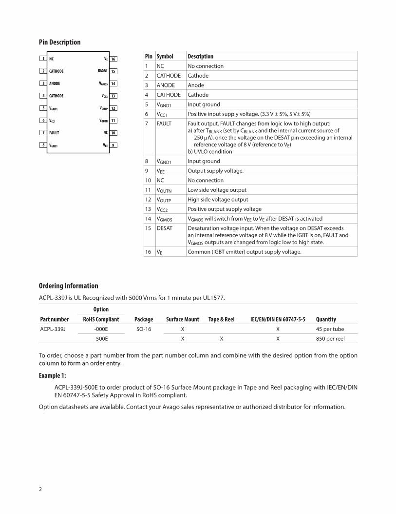
Pin Description
1
2
3
4
5
6
7
8
16
15
14
13
12
11
10
9
VE
DESAT
VCC2
NC
VOUTN
VGMOS
VEE
NC
FAULT
VGND1
CATHODE
VCC1
ANODE
CATHODE
VGND1
VOUTP
Pin Symbol Description1 NC No connection
2 CATHODE Cathode
3 ANODE Anode
4 CATHODE Cathode
5 VGND1 Input ground
6 VCC1 Positive input supply voltage. (3.3 V ± 5%, 5 V± 5%)
7 FAULT Fault output. FAULT changes from logic low to high output:a) after TBLANK (set by CBLANK and the internal current source of 250 µA), once the voltage on the DESAT pin exceeding an internal reference voltage of 8 V (reference to VE)b) UVLO condition
8 VGND1 Input ground
9 VEE Output supply voltage.
10 NC No connection
11 VOUTN Low side voltage output
12 VOUTP High side voltage output
13 VCC2 Positive output supply voltage
14 VGMOS VGMOS will switch from VEE to VE after DESAT is activated
15 DESAT Desaturation voltage input. When the voltage on DESAT exceeds an internal reference voltage of 8 V while the IGBT is on, FAULT and VGMOS outputs are changed from logic low to high state.
16 VE Common (IGBT emitter) output supply voltage.
Ordering InformationACPL-339J is UL Recognized with 5000 Vrms for 1 minute per UL1577.
Part number
Option
Package Surface Mount Tape & Reel IEC/EN/DIN EN 60747-5-5 QuantityRoHS CompliantACPL-339J -000E SO-16 X X 45 per tube
-500E X X X 850 per reel
To order, choose a part number from the part number column and combine with the desired option from the option column to form an order entry.
Example 1:
ACPL-339J-500E to order product of SO-16 Surface Mount package in Tape and Reel packaging with IEC/EN/DIN EN 60747-5-5 Safety Approval in RoHS compliant.
Option datasheets are available. Contact your Avago sales representative or authorized distributor for information.

3
Package Outline DrawingsACPL-339J 16-Lead Surface Mount Package
Recommended Pb-Free IR ProfileRecommended reflow condition as per JEDEC Standard, J-STD-020 (latest revision). Non- Halide Flux should be used.
Regulatory InformationThe ACPL-339J is pending approval by the following organizations:
IEC/EN/DIN EN 60747-5-5Maximum working insulation voltage VIORM = 1414 VPEAK
ULApproval under UL 1577, component recognition program up to VISO = 50000 VRMS. File E55361.
CSAApproval under CSA Component Acceptance Notice #5, File CA 88324.
Dimensions in inches (millimeters)
Notes: Initial and continued variation in the color of the ACPL-339J’s white mold compound is normal and does note affect device performance or reliability.
Floating Lead Protrusion is 0.25 mm (10 mils) max.
9
0.295 ± 0.010(7.493 ± 0.254)
10111213141516
87654321
0.018(0.457)
0.138 ± 0.005(3.505 ± 0.127)
9°
0.406 ± 0.10(10.312 ± 0.254)
0.408 ± 0.010(10.160 ± 0.254)
0.025 MIN.0.008 ± 0.003
(0.203 ± 0.076)STANDOFF
0.345 ± 0.010(8.986 ± 0.254)
0-8°
0.018(0.457)
0.050(1.270)
ALL LEADSTO BECOPLANAR± 0.002
A 339JYYWW
TYPE NUMBERDATE CODE
0.458 (11.63)
0.085 (2.16)
0.025 (0.64 )LAND PATTERN RECOMMENDATION
4
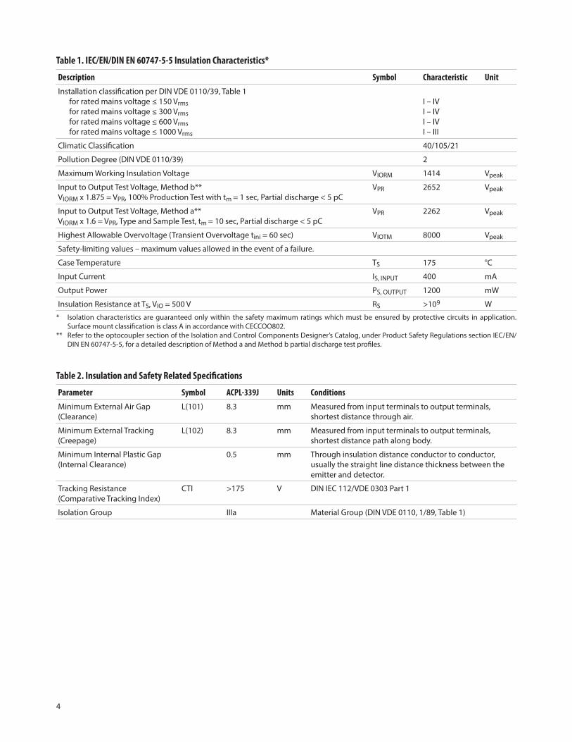
Table 1. IEC/EN/DIN EN 60747-5-5 Insulation Characteristics*
Description Symbol Characteristic UnitInstallation classification per DIN VDE 0110/39, Table 1
for rated mains voltage ≤ 150 Vrmsfor rated mains voltage ≤ 300 Vrmsfor rated mains voltage ≤ 600 Vrmsfor rated mains voltage ≤ 1000 Vrms
I – IVI – IVI – IVI – III
Climatic Classification 40/105/21
Pollution Degree (DIN VDE 0110/39) 2
Maximum Working Insulation Voltage VIORM 1414 Vpeak
Input to Output Test Voltage, Method b**VIORM x 1.875 = VPR, 100% Production Test with tm = 1 sec, Partial discharge < 5 pC
VPR 2652 Vpeak
Input to Output Test Voltage, Method a**VIORM x 1.6 = VPR, Type and Sample Test, tm = 10 sec, Partial discharge < 5 pC
VPR 2262 Vpeak
Highest Allowable Overvoltage (Transient Overvoltage tini = 60 sec) VIOTM 8000 Vpeak
Safety-limiting values – maximum values allowed in the event of a failure.
Case Temperature TS 175 °C
Input Current IS, INPUT 400 mA
Output Power PS, OUTPUT 1200 mW
Insulation Resistance at TS, VIO = 500 V RS >109 W
* Isolation characteristics are guaranteed only within the safety maximum ratings which must be ensured by protective circuits in application. Surface mount classification is class A in accordance with CECCOO802.
** Refer to the optocoupler section of the Isolation and Control Components Designer’s Catalog, under Product Safety Regulations section IEC/EN/DIN EN 60747-5-5, for a detailed description of Method a and Method b partial discharge test profiles.
Table 2. Insulation and Safety Related Specifications
Parameter Symbol ACPL-339J Units ConditionsMinimum External Air Gap (Clearance)
L(101) 8.3 mm Measured from input terminals to output terminals, shortest distance through air.
Minimum External Tracking (Creepage)
L(102) 8.3 mm Measured from input terminals to output terminals, shortest distance path along body.
Minimum Internal Plastic Gap (Internal Clearance)
0.5 mm Through insulation distance conductor to conductor, usually the straight line distance thickness between the emitter and detector.
Tracking Resistance (Comparative Tracking Index)
CTI >175 V DIN IEC 112/VDE 0303 Part 1
Isolation Group IIIa Material Group (DIN VDE 0110, 1/89, Table 1)

5
Table 3. Absolute Maximum Ratings
Parameter Symbol Min. Max. Units NoteStorage Temperature TS -55 125 °C
Operating Temperature TA -40 105 °C
Output IC Junction Temperature TJ 125 °C
Average Input Current IF(AVG) 25 mA 1
Peak Transient Input Current(< 1 µs pulse width, 300 pps)
IF(TRAN) 1.0 A
Reverse Input Voltage VR 5 V
“High” Peak Output Current IOH(PEAK) 5.5 A 2
“Low” Peak Output Current IOL(PEAK) 5.5 A 2
Positive Input Supply Voltage VCC1 0 7 V
FAULT Output Current IFAULT 8 mA
FAULT Pin Voltage VFAULT -0.5 VCC1 V
Total Output Supply Voltage (VCC2 – VEE) 0 35 V
Negative Output Supply Voltage (VE – VEE) 0 17 V
Positive Output Supply Voltage (VCC2 – VE) 0 35 – (VE – VEE) V
High Side Output Voltage VOUTP(PEAK) VE – 0.5 VCC2 + 0.5 V
Low Side Output Voltage VOUTN(PEAK) VEE – 0.5 VE + 0.5 V
DESAT Voltage VDESAT VE – 0.5 VCC2 + 0.5 V
VGMOS Voltage VGMOS VEE – 0.5 VE + 0.5 V
Output IC Power Dissipation PO 600 mW 3
Input LED Power Dissipation PI 150 mW 4
Notes:1. Derate linearly above 70° C free-air temperature at a rate of 0.3 mA/°C.2. Maximum pulse width = 10 µs 3. Derate linearly above 95° C free-air temperature at a rate of 20 mW/°C.4. Derate linearly above 95° C free-air temperature at a rate of 4 mW/°C. The maximum LED junction temperature should not exceed 125° C.
Table 4. Recommended Operating Conditions
Parameter Symbol Min. Max. Units NoteOperating Temperature TA -40 105 °C
Positive input supply voltage VCC1 3.3 5.5 V
Total Output Supply Voltage (VCC2 – VEE) 21 30 V
Negative Output Supply Voltage (VE – VEE) 6 15 V
Positive Output Supply Voltage (VCC2 – VE) 15 30 – (VE – VEE) V
Input Current (ON) IF(ON) 6 10 mA
Input Voltage (OFF) VF(OFF) -3.6 0.8 V

6
Table 5. Electrical Specifications (DC)Unless otherwise noted, all typical values at TA = 25° C, VCC1 = 3.3 V or 5 V, VCC2 – VE = 15 V, VE – VEE = 8 V; all Minimum/Maximum specifications are at Recommended Operating Conditions.
Parameter Symbol Min. Typ. Max. Units Test Conditions Fig. NoteVOUTP High Level Output Current
IOUTPH -1 A VCC2 – VOUTP ≤ 15 V 3 1
VOUTP Low Level Output Current
IOUTPL 1 A VOUTP – VE ≤ 15 V 4 1
VOUTN High Level Output Current
IOUTNH -1 A VE – VOUTN ≤ 8 V 3 1
VOUTN Low Level Output Current
IOUTNL 1 A VOUTN - VEE ≤ 8 V 4 1
VOUTP High Level Output RDSON
ROUTPH 3.5 7 Ω IOUTP = -1 A, VF = 0 V 3, 5 1
VOUTP Low Level Output RDSON
ROUTPL 1.5 4 Ω IOUTP = 1 A, IF = 8 mA 4, 6 1
VOUTN High Level Output RDSON
ROUTNH 3.5 7 Ω IOUTN = -1 A, VF = 0 V 3, 5 1
VOUTN Low Level Output RDSON
ROUTNL 1.5 4 Ω IOUTN = 1 A, IF = 8 mA 4, 6 1
VOUTP High Level Output Voltage
VOUTPH VCC2 – 0.60 VCC2 – 0.30 V IOUTP = -100 mA, VF = 0 V 1 2, 4, 5
VOUTP Low Level Output Voltage
VOUTPL VE + 0.14 VE + 0.50 V IOUTP = 100 mA, IF = 8 mA 2
VOUTN High Level Output Voltage
VOUTNH VE – 0.60 VE – 0.30 V IOUTN = -100 mA, VF = 0 V 1 3, 4, 5
VOUTN Low Level Output Voltage
VOUTNL VEE + 0.12 VEE + 0.60 V IOUTN = 100 mA, IF = 8 mA 2
VGMOS High Level Output Current
IOUTGH -80 mA VE – VGMOS ≤ 8 V, IF = 8 mA, DESAT = Open
VGMOS Low Level Output Current
IOUTGL 80 mA VGMOS – VEE ≤ 8 V, VF = 0 V, DESAT = Open
VGMOS High Level Output RDSON
ROUTGH 22 30 Ω IOUTG = -80 mA, IF = 8 mA 7
VGMOS Low Level Output RDSON
ROUTGL 6 10 Ω IOUTN = 80 mA, VF = 0 V, DESAT = Open
8
VGMOS High Level Output Voltage
VOUTGH VE V IOUTG = 0 mA, IF = 8 mA, DESAT = Open
VGMOS Low Level Output Voltage
VOUTGL VEE V IOUTN = 0 mA, VF = 0 V, DESAT = Open
High Level Output Supply Current (VCC2)
ICC2H 8.5 12 mA VF = 0 V, No Load 9, 10
Low Level Output Supply Current (VCC2)
ICC2L 8.5 12 mA IF = 8 mA, No Load, 9, 10
High Level Output Supply Current (VEE)
IEEH 8 11 mA VF = 0 V, No Load 11, 12
Low Level Output Supply Current (VEE)
IEEL 8 11 mA IF = 8 mA, No Load 11, 12
Threshold Input Current Low to High
IFLH 1.3 5 mA No Load, VOUTP – VE < 5 V, VOUTN – VEE < 1 V
13, 14
Threshold Input Voltage High to Low
VFHL 0.8 V No Load, VOUTP – VE > 5 V, VOUTN – VEE > 1 V

7
Table 5. Electrical Specifications (DC) (continued)
Unless otherwise noted, all typical values at TA = 25° C, VCC1 = 3.3 V or 5 V, VCC2 – VE = 15 V, VE – VEE = 8 V; all Minimum/Maximum specifications are at Recommended Operating Conditions.
Parameter Symbol Min. Typ. Max. Units Test Conditions Fig. NoteInput Forward Voltage VF 1.2 1.55 1.95 V IF = 8 mA
Temperature Coefficient of Input Forward Voltage
ΔVF/ΔTA -1.7 mV/°C IF = 8 mA
Input Reverse Breakdown Voltage
BVR 5 V IR = 100 mA
Input Capacitance CIN 70 pF f = 1 MHz, VF = 0 V
UVLO_P Threshold, VCC2-VE
VUVLOP+ 12 13 14 V IF = 8 mA, VOUTP – VE < 5 V 31 2, 5, 6
VUVLOP- 11 12 13 V IF = 8 mA, VOUTP – VE > 5 V 31 3, 5, 7
UVLO_P Hysteresis, VCC2-VE
VUVLOP+ - VUVLOP-
1 V
UVLO_N Threshold, VE-VEE
VUVLON+ 4.8 5.4 6 V IF = 8 mA, VOUTN – VEE < 1 V 31 2, 5, 8
VUVLON- 4.7 5 5.7 V IF = 8 mA, VOUTN – VEE > 1 V 31 3, 5, 9
UVLO_N Hysteresis, VE-VEE
VUVLON+ - VUVLON-
0.3 V
DESAT Threshold VDESAT 7.5 8 9 V VCC2 – VE > VUVLOP-and VE – VEE > VUVLON-
15 5
Blanking CapacitorCharging Current
ICHG 0.15 0.25 0.36 mA VDESAT = 2 V 16 5, 10
DESAT Low Voltage when Blanking Capacitor Discharge
VDSCHG 1.1 3 V IDSCHG = 10 mA 5, 10
FAULT Logic Low Output Voltage
VFAULTL 0.10 0.25 V VDESAT = 0 V, RF = 10 kΩ, CF = 1 nF, VCC1 = 5 V or 3.3 V
FAULT Logic High Output Voltage
VFAULTH VCC1 V DESAT = Open, RF = 10 kΩ, CF = 1 nF, VCC1 = 5 V or 3.3 V
FAULT Logic Low Output Current
IFAULTL 0.25 mA VFAULT = 0.15 V, VCC1 = 5 V or 3.3 V
FAULT Logic High Output Current
IFAULTH 0.2 1 µA VFAULT = VCC1 = 5 V or 3.3 V
Notes:1. Output is sourced at -1.0 A / 1.0 A with a maximum pulse width = 10 µs.2. 15 V is the recommended minimum operating positive supply voltage (VCC2 – VE) to ensure adequate margin in excess of the maximum VUVLOP+
threshold of 13.5 V. For High Level Output Voltage testing, VOUTP is measured with a 50 µs pulse load current. When driving capacitive loads, VOUTP will approach VCC as IOUTPH approaches zero units.
3. 6.6 V is the recommended minimum operating positive supply voltage (VE – VEE) to ensure adequate margin in excess of the maximum VUVLON+ threshold of 5.6 V. For High Level Output Voltage testing, VOUTN is measured with a 50 µs pulse load current. When driving capacitive loads, VOUTN will approach VE as IOUTNH approaches zero units.
4. Maximum pulse width = 1.0 ms.5. Once VOUTP is allowed to go low (VCC2 – VE > VUVLOP+) and VOUTN is allowed to go high (VE – VEE > VUVLON+), the DESAT detection feature of the
ACPL-339J will be the primary source of IGBT protection. UVLO is needed to ensure DESAT is functional. Once VCC2 – VE > VUVLOP+ and VE – VEE > VUVLON+, DESAT will remain functional until VCC2 – VE < VUVLOP- or VE – VEE < VUVLON-,. Thus, the DESAT detection and UVLO features of the ACPL-339J work in conjunction to ensure constant IGBT protection.
6. This is the “increasing” (i.e. turn-on or “positive going” direction) of VCC2 – VE.7. This is the “decreasing” (i.e. turn-off or “negative going” direction) of VCC2 – VE.8. This is the “increasing” (i.e. turn-on or “positive going” direction) of VEE – VE.9. This is the “decreasing” (i.e. turn-ff or “negative going” direction) of VEE – VE.10. See the DESAT fault detection blanking time section in the applications notes at the end of this data sheet for further details.

8
Table 6. Switching Specifications (AC)Unless otherwise noted, all typical values at TA = 25° C, VCC1 = 3.3 V or 5 V, and VCC2 – VE = 15 V, VE – VEE = 8 V; all Minimum/Maximum specifications are at Recommended Operating Conditions.
Parameter Symbol Min. Typ. Max. Units Test Conditions Fig. NotePropagation Delay Time to High Output Level
tPLH 100 180 300 ns CP = CN = 4 nF, f = 20 kHz, Duty Cycle = 50%, IF = 6 mA to 10 mA
17, 18, 30 1
Propagation Delay Time to Low Output Level
tPHL 100 150 300 ns 17, 18, 30 1
Pulse Width Distortion PWD 150 25 150 ns 2
Propagation Delay Difference Between Any Two Parts
PDD (tPLH – tPHL)
-200 200 ns 36, 37 3
LED OFF to 90% of VOUTP tDP 50 150 250 ns 17,18, 30
LED ON to 10% of VOUTN tDN 50 125 250 ns 17,18, 30
Non-overlap Time Low to High tNLH 30 ns 25, 30
Non-overlap Time High to Low tNHL 20 ns 25, 30
10% to 90% Rise Time on VOUTP tPR 40 ns CP = CN = 4 nF, f = 20 kHz, Duty Cycle = 50%, IF = 8 mA
30
90% to 10% Fall Time on VOUTP tPF 40 ns 30
10% to 90% Rise Time on VOUTN tNR 40 ns 30
90% to 10% Fall Time on VOUTN tNF 30 ns 30
Delay time from DESAT threshold to 50% of High VGMOS
t1 250 500 ns CP = CN = 4 nF, CG = 1 nF, f = 250 Hz, Duty Cycle = 50%, IF = 8 mA
19, 22, 28, 29
Delay time from DESAT threshold to 50% of High VOUTP
t2 250 500 ns 19, 28, 29
Delay time from DESAT threshold to 50% of High FAULT
t3 8.5 11 µs RF = 10 kΩ, CF = 1 nF, VCC1 = 3.3 V or 5 V, f = 250 Hz, Duty Cycle = 50%, IF = 8 mA
20, 28, 29
Delay from 50% of VGMOS to 50% of VOUTN
t4 11 ns CP = CN = 4 nF, CG = 1 nF, f = 250 Hz, Duty Cycle = 50%, IF = 8 mA
21, 23, 28, 29
Mute time tMUTE 0.75 1 1.5 ms f = 700 Hz, Duty Cycle = 50%, IF = 8 mA
24, 28, 29 4
Output High Level Common Mode Transient Immunity
|CMH| 25 35 kV/µs TA = 25° C, VCM = 1500 V, VCC1 = 5 V, CF = 1 nF, RF = 10 kΩ, IF = 8 mA with split resistors
5
Output Low Level Common Mode Transient Immunity
|CML| 25 35 kV/µs TA = 25° C, VCM = 1500 V, VCC1 = 5 V, CF = 1 nF, RF = 10 kΩ, VF = 0 V
6
Notes:1. This load condition approximates the gate load of a 60V/5A MOSFET2. Pulse Width Distortion (PWD) is defined as |tPHL – tPLH| for any given unit. 3. The difference between tPHL and tPLH between any two ACPL-339J parts under the same test conditions.4. Auto Reset: This is the minimum amount of time when VOUTP will be asserted high, VOUTN asserted low, VGMOS asserted high and FAULT asserted
high, after DESAT threshold is exceeded. See the Description of Operation (Auto Reset) topic in the application information section.5. Common mode transient immunity in the high state is the maximum tolerable dVCM/dt of the common mode pulse, VCM, to assure that the output
will remain in the high state (i.e., VOUTP – VE > 12 V, VOUTN – VEE > 5 V or FAULT > 2 V). A 1 nF and a 10 kΩ pull-up resistor is needed in fault detection mode.
6. Common mode transient immunity in the low state is the maximum tolerable dVCM/dt of the common mode pulse, VCM, to assure that the output will remain in a low state (i.e., VOUTP – VE < 1.0 V, VOUTN – VEE < 1.0 V or FAULT < 0.8 V).

9
0
VF = 0 VIOUT = -100 mA
0
0.05
0.1
0.15
0.2
0.25
0.3
0.35
0.4
HIGH
OUT
PUT V
OLTA
GE D
ROP
- V
-40 -20 0 25 50 85 105TA - TEMPERATURE - °C
-40 -20 0 25 50 85 105TA - TEMPERATURE - °C
VOUTNH-VEVOUTPH-VCC2
VF = 0 VTA = 25° C
IOUTNHIOUTPH
IF = 8 mATA = 25° C IOUTNL
IOUTPL
IF = 8 mAIOUT = 100 mA VOUTNL-VEE
VOUTPL-VE
00.020.040.060.08
0.10.120.140.160.18
0.2
LOW
OUTP
UT V
OLTA
GE D
ROP
- V
-2.5
-2
-1.5
-1
-0.5
0
OUTP
UT H
IGH
CURR
ENT -
A
VOUTPH-VCC2/VOUTNH-VE - V-15-14-12-10-8-6-4-2
0
0.5
1
1.5
2
2.5
3
OUTP
UT LO
W CU
RREN
T - A
0VOUTPL-VE/VOUTNL-VEEE - V
151412108642
Table 7. Package Characteristics
Parameter Symbol Min. Typ. Max. Units Test Conditions Fig. NoteInput-Output Momentary Withstand Voltage
VISO 5000 Vrms RH < 50%,t = 1 min., TA = 25° C
1, 2
Input-Output Resistance RI-O > 109 W VI-O = 500 V 2
Input-Output Capacitance CI-O 1.3 pF freq =1 MHz
Notes1. In accordance with UL1577, each optocoupler is proof tested by applying an insulation test voltage ≥ 6000 Vrms for 1 second. This test is performed
before the 100% production test for partial discharge (method b) shown in IEC/EN/DIN EN 60747-5-5 Insulation Characteristic Table, if applicable.2. Device considered a two-terminal device: pins 1 to 8 are shorted together and pins 9 to 16 are shorted together.
Figure 1. VOUTPH/VOUTNH vs. temperature Figure 2. VOUTPL/VOUTNL vs. temperature
Figure 3. IOUTPH/IOUTNH vs.VOUTPH/VOUTNH Figure 4. IOUTPL/IOUTNL vs.VOUTPL/VOUTNL
10
VF = 0 VIOUT = -1 A
ICC2LICC2H
IF = 8 mAIOUT = 1 A ROUTNL
ROUTPL
VCC2-VE - V
-40 -20 0 25 50 85 105TA - TEMPERATURE - °C
-40 -20 0 25 50 85 105TA - TEMPERATURE - °C
-40 -20 0 25 50 85 105TA - TEMPERATURE - °C
-40 -20 0 25 50 85 105TA - TEMPERATURE - °C
TA - TEMPERATURE - °C
00.5
11.5
22.5
33.5
44.5
5HI
GH O
UTPU
T RDS
ON - Ω
ROUTNHROUTPH
0
0.5
1
1.5
2
2.5
LOW
OUT
PUT R
DSON
- Ω
IF = 8 mAIOUTG = -80 mA
0
5
10
15
20
25
30
V GM
OS H
IGH
OUT
PUT R
DSON
- Ω
V GM
OS LO
W O
UTPU
T RDS
ON - Ω
VF = 0 VIOUTG = -80 mADESAT = OPEN
-40 -20 0 25 50 85 1050123456789
10
8.38.35
8.48.45
8.58.55
8.68.65
8.78.75
8.8
V CC2
SUPP
LY CU
RREN
T - m
A
VF = 0 V (ICC2H)IF = 8 mA (ICC2L)
IF = 8 mA (ICC2L)VF = 0 V (ICC2H)TA = 25° CVE-VEE = 6 V ICC2H
ICC2L
8.15
8.2
8.25
8.3
8.35
8.4
8.45
8.5
8.55
8.6
V CC2
SUPP
LY CU
RREN
T - m
A
15 16 17 18 19 20 21 22 23 24
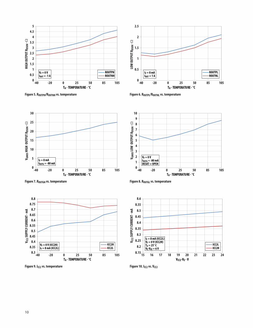
Figure 5. ROUTPH/ROUTNH vs. temperature Figure 6. ROUTPL/ROUTNL vs. temperature
Figure 7. ROUTGH vs. temperature Figure 8. ROUTGL vs. temperature
Figure 9. ICC2 vs. temperature Figure 10. ICC2 vs. VCC2

11
VF = 0 V (IEEH)IF = 8 mA (IEEL)
-40 -20 0 25 50 85 105TA - TEMPERATURE - °C
-40 -20 0 25 50 85 105TA - TEMPERATURE - °C
IEELIEEH
IEEHIEEL
VOUTNVOUTP
IFLH OFFIFLH ON
-40 -20 0 25 50 85 105TA - TEMPERATURE - °C
-40 -20 0 25 50 85 105TA - TEMPERATURE - °C
VE-VEE - V
8.15
8.2
8.25
8.3
8.35
8.4
8.45
8.5
8.55V E
E SUP
PLY C
URRE
NT - m
A
6 7 8 9 10 11 12 13 14 15
IF = 8 mA (IEEL)VF = 0 V (IEEH)TA = 25° CVCC2-VE = 15 V
8
7.9
7.95
8.05
8.1
8.15
8.2
8.25
8.3
V EE S
UPPL
Y CUR
RENT
- mA
-10
-5
0
5
10
15
20
V OUT
P/V O
UTN O
UT V
OLTA
GE - V
LOW TO HIGH INPUT CURRENT THRESHOLD - mA
TA = 25° C
0 0.5 1 1.5 2 2.5 3
LOW
TO H
IGH
CURR
ENT T
HRES
HOLD
- mA
0
0.5
1
1.5
2
2.5
8.04
8.06
8.08
8.1
8.12
8.14
8.16
8.18
V DES
AT D
ESAT
THRE
SHOL
D - V
210
215
220
225
230
235
I CHGB
LANK
ING
CAPA
CITO
R CH
ARGI
NG
CURR
ENT -
µA
Figure 11. IEE vs. temperature Figure 12. IEE vs. VEE
Figure 13. VOUTPH/VOUTNH vs. IFLH Figure 14. IFLH vs. temperature
Figure 15. VDESAT vs. temperature Figure 16. ICHG vs. temperature

12
-40 -20 0 25 50 85 105TA - TEMPERATURE - °C
-40 -20 0 25 50 85 105TA - TEMPERATURE - °C
-40 -20 0 25 50 85 105TA - TEMPERATURE - °C
-40 -20 0 25 50 85 105TA - TEMPERATURE - °C
CP/CN = 4 nFf = 20 kHzDC = 50%
tPHLtPLHtDPtDN
CP/CN = 4 nFf = 250 HzDC = 50%
t1t2
tPHLtPLHtDPtDN
0
50
100
150
200
250t P
/t D P
ROPA
GATI
ON D
ELAY
- ns
0
50
100
150
200
250
t P/t D
PRO
PAGA
TION
DEL
AY - n
s
IF = 8 mATA = 25° Cf = 20 kHzDC = 50%
CP/CN - LOAD CAPACITANCE - nF0 2 4 6 8 10 12
CG - LOAD CAPACITANCE - nF
0
50
100
150
200
250
300
350
t 1/t 2
DEL
AY TI
ME -
ns
7
7.5
8
8.5
9
9.5
10
t 3 D
ELAY
TIM
E - n
s
CF = 1 nFRF = 10 kΩf = 250 HzDC = 50%
CP/CN = 4 nFIF = 8 mATA = 25° Cf = 250 HzDC = 50%
CG = 1 nFf = 250 HzDC = 50%
t 4 D
ELAY
TIM
E - n
s
0
2
4
6
8
10
12
14
16
0
50
100
150
200
250
300
350
400
450
t 1 D
ELAY
TIM
E - n
s
1 2 3 4 5 6 7 8 9 10
Figure 17. tP /tD vs. temperature Figure 18. tP /tD vs. CP/CN
Figure 19. t1 /t2 vs. temperature Figure 20. t3 vs. temperature
Figure 21. t4 vs. temperature Figure 22. t1 vs. CG

13
-40 -20 0 25 50 85 105TA - TEMPERATURE - °C
f = 700 HzDC = 50%
IF = 8 mATA = 25° Cf = 250 HzDC = 50%
0
5
10
15
20
25
30
35
40
1 2 3 4 5 6 7 8 9 10
t 4 D
ELAY
TIM
E - n
s
CN/CG - LOAD CAPACITANCE - nF
0.860.88
0.90.920.940.960.98
11.021.041.061.08
t MUT
E MUT
E TIM
E - m
s
-40 -20 0 25 50 85 105TA - TEMPERATURE - °C
0
5
10
15
20
25
30
35
t NLH
/t NHL
NON
-OVE
RLAP
TIM
E - n
s
tNHLtNLH
CP/CN = 4 nFf = 20 kHzDC = 50%
Figure 23. t4 vs. CN /CG Figure 24. tMUTE vs. temperature
Figure 25. tNLH/tNHL vs. temperature
14
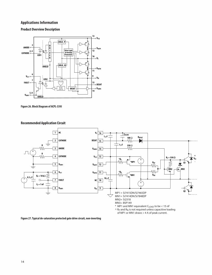
Applications Information
Product Overview Description
Figure 26. Block Diagram of ACPL-339J
Recommended Application Circuit
Figure 27. Typical de-saturation protected gate drive circuit, non-inverting
MP1 = Si7415DN/Si7465DPMN1 = Si7414DN/Si7848DPMN2 = Si2318MN3 = BSP149* MP1 and MN1 equivalent CLOAD to be < 15 nF^ RP and RN is not required unless capacitive loading of MP1 or MN1 draws > 4 A of peak current.
13
SHIELD
SHIELD
DRIVER
DESAT
VCC2
VOUTP
VEEVCC1
VGND1
FAULT
ANODE
CATHODE
VGMOS
3
2, 4
6
7
5, 8
12
16
15
14
UVLO_P
LED1
LED2
VE
VOUTN11
9
UVLO_N
DESAT
Drive Logic& Overlap
Protection
1
2
3
4
5
6
7
8
16
15
14
13
12
11
10
9
VE
DESAT
VCC2
NC
VOUTN
VGMOS
VEE
NC
FAULT
VGND1
CATHODE
VCC1
ANODE
CATHODE
VGND1
VOUTP
+_
+_
R
R
RF = 10 kΩ
RS = 330 Ω
0.3 µF
CF = 1 nF
+_
+_
100 Ω
330 Ω
^RP
^RN
RGP
RGN
CBLANKDDESAT
Q1
+VCE_
1 µF
1 µF
10 µF
*MP1
*MN1
MN2 MN3
Q2
15
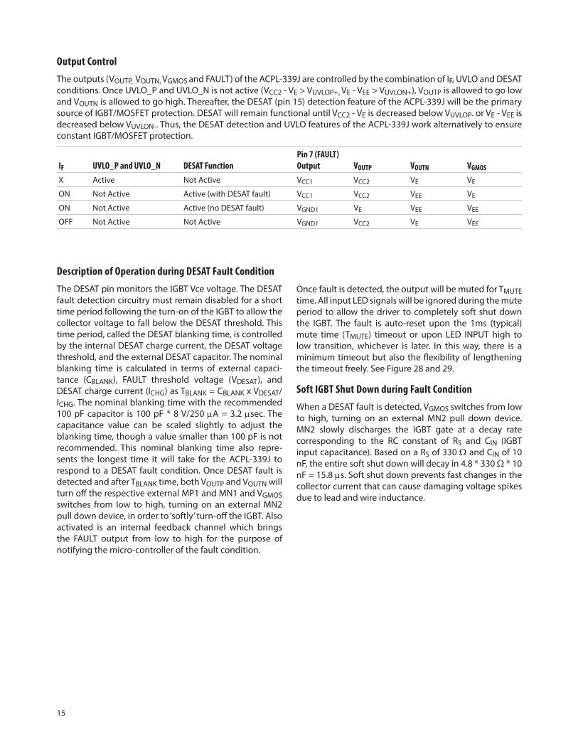
Output ControlThe outputs (VOUTP, VOUTN, VGMOS and FAULT) of the ACPL-339J are controlled by the combination of IF, UVLO and DESAT conditions. Once UVLO_P and UVLO_N is not active (VCC2 - VE > VUVLOP+, VE - VEE > VUVLON+), VOUTP is allowed to go low and VOUTN is allowed to go high. Thereafter, the DESAT (pin 15) detection feature of the ACPL-339J will be the primary source of IGBT/MOSFET protection. DESAT will remain functional until VCC2 - VE is decreased below VUVLOP- or VE - VEE is decreased below VUVLON-. Thus, the DESAT detection and UVLO features of the ACPL-339J work alternatively to ensure constant IGBT/MOSFET protection.
IF UVLO_P and UVLO_N DESAT FunctionPin 7 (FAULT) Output VOUTP VOUTN VGMOS
X Active Not Active VCC1 VCC2 VE VE
ON Not Active Active (with DESAT fault) VCC1 VCC2 VEE VE
ON Not Active Active (no DESAT fault) VGND1 VE VEE VEE
OFF Not Active Not Active VGND1 VCC2 VE VEE
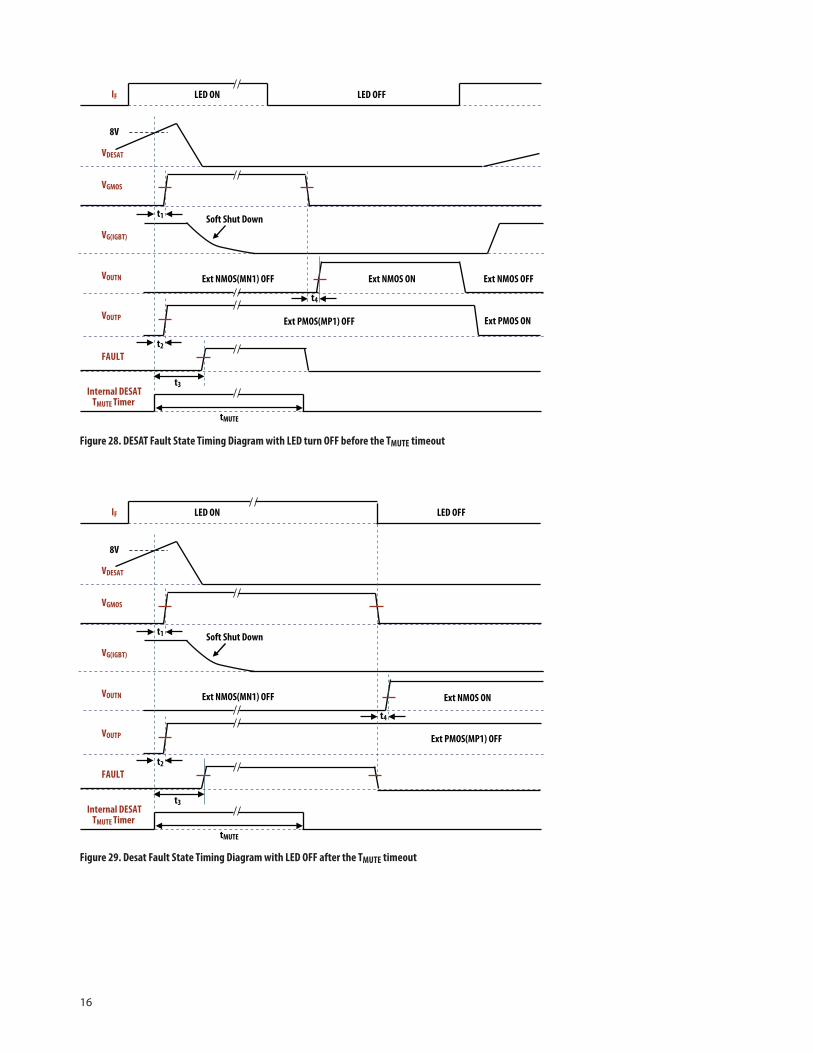
Description of Operation during DESAT Fault ConditionThe DESAT pin monitors the IGBT Vce voltage. The DESAT fault detection circuitry must remain disabled for a short time period following the turn-on of the IGBT to allow the collector voltage to fall below the DESAT threshold. This time period, called the DESAT blanking time, is controlled by the internal DESAT charge current, the DESAT voltage threshold, and the external DESAT capacitor. The nominal blanking time is calculated in terms of external capaci-tance (CBLANK), FAULT threshold voltage (VDESAT), and DESAT charge current (ICHG) as TBLANK = CBLANK x VDESAT/ICHG. The nominal blanking time with the recommended 100 pF capacitor is 100 pF * 8 V/250 µA = 3.2 µsec. The capacitance value can be scaled slightly to adjust the blanking time, though a value smaller than 100 pF is not recommended. This nominal blanking time also repre-sents the longest time it will take for the ACPL-339J to respond to a DESAT fault condition. Once DESAT fault is detected and after TBLANK time, both VOUTP and VOUTN will turn off the respective external MP1 and MN1 and VGMOS switches from low to high, turning on an external MN2 pull down device, in order to ‘softly’ turn-off the IGBT. Also activated is an internal feedback channel which brings the FAULT output from low to high for the purpose of notifying the micro-controller of the fault condition.
Once fault is detected, the output will be muted for TMUTE time. All input LED signals will be ignored during the mute period to allow the driver to completely soft shut down the IGBT. The fault is auto-reset upon the 1ms (typical) mute time (TMUTE) timeout or upon LED INPUT high to low transition, whichever is later. In this way, there is a minimum timeout but also the flexibility of lengthening the timeout freely. See Figure 28 and 29.
Soft IGBT Shut Down during Fault ConditionWhen a DESAT fault is detected, VGMOS switches from low to high, turning on an external MN2 pull down device. MN2 slowly discharges the IGBT gate at a decay rate corresponding to the RC constant of RS and CIN (IGBT input capacitance). Based on a RS of 330 Ω and CIN of 10 nF, the entire soft shut down will decay in 4.8 * 330 Ω * 10 nF = 15.8 µs. Soft shut down prevents fast changes in the collector current that can cause damaging voltage spikes due to lead and wire inductance.
16
Figure 28. DESAT Fault State Timing Diagram with LED turn OFF before the TMUTE timeout
Figure 29. Desat Fault State Timing Diagram with LED OFF after the TMUTE timeout
8V
IF
VDESAT
VGMOS
FAULT
LED ON LED OFF
tMUTE
Internal DESATTMUTE Timer
VOUTP Ext PMOS(MP1) OFF Ext PMOS ON
Ext NMOS ONExt NMOS(MN1) OFF Ext NMOS OFFVOUTN
t1
t3
VG(IGBT)
Soft Shut Down
t2
t4
8V
IF
VDESAT
VGMOS
FAULT
LED ON LED OFF
tMUTE
Internal DESATTMUTE Timer
VOUTP Ext PMOS(MP1) OFF
Ext NMOS ONExt NMOS(MN1) OFFVOUTN
t1
t3
VG(IGBT)
Soft Shut Down
t2
t4
17
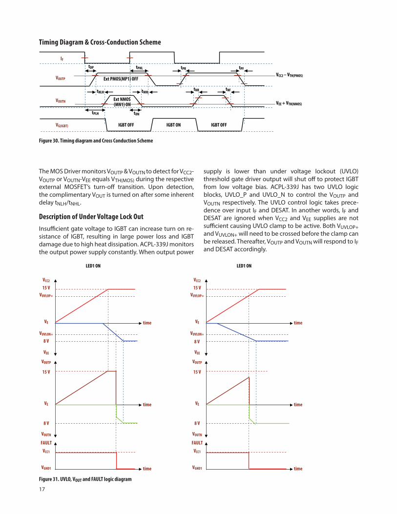
Timing Diagram & Cross-Conduction Scheme
Figure 30. Timing diagram and Cross Conduction Scheme
The MOS Driver monitors VOUTP & VOUTN to detect for VCC2-VOUTP or VOUTN-VEE equals VTH(MOS) during the respective external MOSFET’s turn-off transition. Upon detection, the complimentary VOUT is turned on after some inherent delay tNLH/tNHL.
Description of Under Voltage Lock OutInsufficient gate voltage to IGBT can increase turn on re-sistance of IGBT, resulting in large power loss and IGBT damage due to high heat dissipation. ACPL-339J monitors the output power supply constantly. When output power
tPLH
tPHLtDP
IGBT OFF IGBT ON
tDN
tPR
IF
VOUTP
VOUTN
VG(IGBT)
tNR
tPF
tNF
IGBT OFF
tNLH tNHL
Ext PMOS(MP1) OFF
Ext NMOS (MN1) ON
VCC2 – VTH(PMOS)
VEE + VTH(NMOS)
supply is lower than under voltage lockout (UVLO) threshold gate driver output will shut off to protect IGBT from low voltage bias. ACPL-339J has two UVLO logic blocks, UVLO_P and UVLO_N to control the VOUTP and VOUTN respectively. The UVLO control logic takes prece-dence over input IF and DESAT. In another words, IF and DESAT are ignored when VCC2 and VEE supplies are not sufficient causing UVLO clamp to be active. Both VUVLOP+ and VUVLON+ will need to be crossed before the clamp can be released. Thereafter, VOUTP and VOUTN will respond to IF and DESAT accordingly.
Figure 31. UVLO, VOUT and FAULT logic diagram
VCC2
VEE
VE time
VOUTP
LED1 ON
VOUTN
VE time
VUVLOP+
VUVLON+
15 V
8 V
15 V
FAULT
VGND1 time
VCC1
VCC2
VEE
VE time
VOUTP
LED1 ON
VOUTN
VE time
VUVLOP+
VUVLON+
15 V
15 V
FAULT
VGND1 time
VCC1
8 V 8 V
8 V

18
Drive and Shutdown MOSFET SelectionThe MOSFETs, MP1 and MN1 driving strength can be estimated by the gate charge and desired charge time needed. The equation below shows an example of this:
Qg = ICHARGE x TCHARGE Qg is the total gate charge that can be picked readily from the IGBT data sheets.
For a 1200/50 A IGBT, the typical Qg is approximately 300 nC and for desired charging time of 200 ns, the ICHARGE will be,
ICHARGE = 300 nC / 200 ns = 1.5 A
The charging current calculated is an average current. The peak gate current of the MOSFET driver can be estimated using the rule of thumb of doubling the ICHARGE. So for this example, a 3 A peak current MOSFET driver rating will be appropriate.
Listed in the table below, are some recommended MOSFET ratings and part numbers suitable for their respective IGBT class.
Applications IGBT Class Qg
Estimated Peak Charging Current MN1 MP1 MN2 MN3
Low Power 1200 V / 50 A 300 nC 3A Sanyo ECH8619
SanyoECH8619
VishaySI2308
SiemensBSS159
Mid Power 1200 V / 300 A 2000 nC 8A VishaySI7414
VishaySI7415
VishaySI2308
SiemensBSS159
High Power 1200 V / 600 A 4000 nC 16A VishaySIS434
VishaySI7611
FairchildFDC5612
CLARECPC3703
Selecting the Gate Resistor (RG)The IGBT switching time is determined by the charging and discharging of the gate of the IGBT. Higher gate peak current will decrease the turn-on and turn-off time and hence reduce the the switching losses. The charging and discharging currents are controlled by the gate resistors RGP and RGN respectively. The RG must be able to limit the peak current below the maximum allowed for the PMOS(MP1) and NMOS(MN1). The internal RDSON of MP1 and MN1 must be taken into account when calculating the peak current.
RGP ≥ – RDSONPVCC – VEEIOP(MAX)
RGN ≥ – RDSONNVCC – VEEION(MAX)
Other Recommended ComponentsThe application circuit in Figure 27 includes a depletion-mode MOSFET, a DESAT pin protection resistor, FAULT pin capacitor and pull-up resistor, false FAULT prevention diodes.

19
Split Resistors Input LED Drive CircuitFigure 32 shows the recommended drive circuit that gives optimum common-mode rejection. The two current setting resistors balance the common mode impedances at the LED’s anode and cathode. This helps to equalize the common mode voltage change at the anode and cathode.
Figure 32. Split Resistors Input LED Drive Circuit
DESAT Diode and DESAT ThresholdThe DESAT diode’s function is to conduct forward cur rent, allowing sensing of the IGBT’s saturated collector-to-emitter voltage, VCESAT, (when the IGBT is “on”) and to block high voltages (when the IGBT is “off”).
During IGBT switching off and towards the end of the forward conduction of the DESAT diode, a reverse current flow for short time. This reverse recovery effect causes the diode not able to achieve its blocking capability until the mobile charge in the junction is depleted. During this time, there is commonly a very high dVCE/dt voltage ramp rate across the IGBT’s collector-to-emitter. This results in ICHARGE = CD-DESAT x dVCE/dt charging current which will charge the blanking capacitor, CBLANK. In order to minimize this charging current and avoid false DESAT triggering, it is best to use fast response diodes. Listed in the below table are fast-recovery diodes that are suitable for use as a DESAT diode (DDESAT).
In the recommended appli cation circuit shown in Figure 27, the voltage on pin 15 (DESAT) is VDESAT = VF + VCE, (where VF is the forward ON voltage of DDESAT and VCE is the IGBT collector-to-emit ter voltage). The value of VCE which triggers DESAT to signal a FAULT condition, is nominally 8 V – VF. If desired, this DESAT threshold voltage can be decreased by using multiple DESAT diodes or low voltage zener diode in series. If n is the number of DE SAT diodes, the nominal threshold value becomes VCE,FAULT(TH) = 8 V – n x VF. If zener diode is used, the nominal threshold value becomes VCE,FAULT(TH) = 8 V – VF – Vz. In the case of using two diodes instead of one, diodes with half of the total required maximum reverse-voltage rating may be chosen.
Depletion-mode MOSFETDuring start-up, the supplies across VCC2 and VEE build up slowly from 0V. It will be harmful to allow the gate driver output to turn on at low supply voltages. UVLO protec-tion kicks in to prevent ACPL-339J outputs from turning on until the supplies reach the UVLO thresholds. But IGBT or Power MOSFET can still be triggered by Miller effect developed by any high dV/dt noise across collector and emitter pins. This miss-triggering can be prevented by de-pletion-mode MOSFET, MN3. A depletion-mode MOSFET will conduct even if its gate voltage is at 0V with respect to its source pin voltage. During start-up, the VGMOS output voltage stays high, at VE, to turn on MN3 to shunt away any miller current that appears at the IGBT gate. This will prevent the IGBT from miss-triggering. After the supplies cross the UVLO thresholds, VGMOS output voltage will at VEE to turn off MN3 and resume normal Inverter opera-tions. MN3 is optional for extra protection. Figure 33. DESAT Diode and DESAT threshold
16
15
14
VE
DESAT
VGMOS
100 Ω CBLANK DDESAT
Q1
+VCE–
DZENER
Part Number Manufacturer trr(ns)Max. Reverse Voltage Rating, VRRM (Volts) Package Type
MUR1100E Motorola 75 1000 59-04 (axial leaded)
MURS160T3 Motorola 75 600 Case 403A (surface mount)
UF4007 General Semi. 75 1000 DO-204AL (axial leaded)
BYM26E Philips 75 1000 SOD64 (axial leaded)
BYV26E Philips 75 1000 SOD57 (axial leaded)
BYV99 Philips 75 600 SOD87 (surface mount)
1
2
3
4
5
NC
VGND1
CATHODE
ANODE
CATHODE
R1
R2µC
+5 V
VDD = 5.0 V:R1 = 287 Ω ±1%R2 = 143 Ω ±1%R1/R2 ≈ 2

20
DESAT Pin Protection ResistorThe freewheeling of flyback diodes connected across the IGBTs can have large instantaneous forward voltage transients which greatly exceed the nominal forward voltage of the diode. This may result in a large negative voltage spike on the DESAT pin which will draw substan-tial current out of the driver if protection is not used. To limit this current to levels that will not damage the driver IC, a 100 ohm resistor should be inserted in series with the DESAT diode. The added resistance will not alter the DESAT threshold or the DESAT blanking time.
False Fault Prevention DiodesOne of the situations that may cause the driver to generate a false fault signal is if the substrate diode of the driver becomes forward biased. This can happen if the reverse recovery spikes coming from the IGBT freewheel-ing diodes bring the DESAT pin below ground. Hence the DESAT pin voltage will be ‘brought’ above the threshold voltage. This negative going voltage spikes is typically generated by inductive loads or reverse recovery spikes of the IGBT/MOSFETs free-wheeling diodes. In order to prevent a false fault signal, it is highly recommended to connect a zener diode and schottky diode across the DESAT pin and VE pin
This circuit solution is shown in Figure 34. The schottky diode will prevent the substrate diode of the gate driver optocoupler from being forward biased while the zener diode (value around 7.5 to 8 V) is used to prevent any positive high transient voltage to affect the DESAT pin.
Figure 34. False fault prevention diodes
FAULT Pin Capacitor and Pull-up ResistorUVLO fault is feedback to the FAULT pin through LED2. If LED2 is normally-off during normal operation, a VCC2 or VEE power supplies fault might result in insufficient drive current to turn on LED2 to report the UVLO fault. To avoid such a condition, LED2 need to be normally-on during normal operations. To reduce power consump-tion, LED2 operates at 50% duty cycle at a frequency of 5 MHz provided by an internal oscillator. A RC network at the FAULT pin is required to filter this oscillation to read a stable “low” for no fault condition.
The RC network consists of a FAULT pin capacitor, CF and a pull-up resistor RF. To achieve effective filtering and high CMR, a 1 nF capacitor should be connected between the FAULT pin and ground, and a 10 KΩ pull-up resistor between FAULT pin and VCC1.
Due to the active “high” FAULT logic, the FAULT pins of more than one ACPL-339J cannot be tied together to achieve a common FAULT signal for the controller. An ‘OR’ing circuit shown in Figure 35 can be used to overcome the problem.
Figure 35. ‘OR’ing the FAULT outputs
16
15
14
VE
DESAT
VGMOS
100 Ω CBLANK DDESAT
Q1
10 V Zener1N5925A
Schottky Diode
MBR0540+
VCE–
6
7
8
FAULT
VCC1
VGND1
RF = 10 kΩ
RF = 10 kΩ
CF = 1 nF
CF = 1 nF
47 kΩ
+_0.3 µF5 V
4.7 kΩ
6
7
8
FAULT
VCC1
VGND1
47 kΩ
+_0.3 µF5 V
4.7 kΩ
ACPL-339J
ACPL-339J
IC1
IC2
FAULT

21
Dead Time and Propagation Delay SpecificationsThe ACPL-339J includes a Propagation Delay Difference (PDD) specification intended to help designers minimize “dead time” in their power inverter designs. Dead time is the time period during which both the high and low side power transistors (Q1 and Q2 in Figure 37) are off. Any overlap in Q1 and Q2 conduction will result in large currents flowing through the power devices between the high and low voltage motor rails.
Figure 36. Minimum LED skew for zero dead time
tPLH MAX
tPHL MIN
Q1 IGBT OFF Q1 IGBT ON
VOUTP 1
VOUTN 1
VG(IGBT) Q1
LED1 IF 1
tPHL MIN
VOUTP 2
VOUTN 2
tPLH MAX
tPLH MAX
tPHL MIN
Q2 IGBT OFFQ2 IGBT ON
PDD= tPLH MAX - tPHL MIN
PDD= tPLH MAX - tPHL MIN
VG(IGBT) Q2
LED2 IF 2
To minimize dead time in a given design, the turn on of LED2 should be delayed (relative to the turn off of LED1) so that under worst-case conditions, transistor Q1 has just turned off when transistor Q2 turns on, as shown in Figure 36. The amount of delay necessary to achieve this condition is equal to the maximum value of the propa-gation delay difference specification, PDDMAX, which is specified to be 200 ns over the operating temperature range of -40° C to 105° C.

22
tPLH MIN
tPHL MIN
Q1 IGBT OFF
Q1 IGBT ON
VOUTP 1
VOUTN 1
VG(IGBT) Q1
LED1 IF 1
tPHL MAX
VOUTP 2
VOUTN 2
tPLH MIN
tPLH MIN
tPHL MAX
Q2 IGBT OFF
Q2 IGBT ONVG(IGBT) Q2
LED2 IF 2
Max. Dead Time = PDDMAX – PDDMIN
Max. Dead Time = PDDMAX – PDDMIN
Figure 37. Waveforms for dead time
Delaying the LED signal by the maximum propagation delay difference ensures that the minimum dead time is zero, but it does not tell a designer what the maximum dead time will be. The maximum dead time is equivalent to the difference between the maximum and minimum propagation delay difference specifications as shown in Figure 37. The maximum dead time for the ACPL-339J is 400 ns (= 200 ns – (-200 ns)) over an operating tempera-ture range of -40° C to 105° C.
Note that the propagation delays used to calculate PDD and dead time are taken at equal temperatures and test conditions since the optocouplers under consideration are typically mounted in close proximity to each other and are switching identical IGBTs.
For product information and a complete list of distributors, please go to our web site: www.avagotech.com
Avago, Avago Technologies, and the A logo are trademarks of Avago Technologies in the United States and other countries.Data subject to change. Copyright © 2005-2013 Avago Technologies. All rights reserved. AV02-3784EN - March 13, 2013
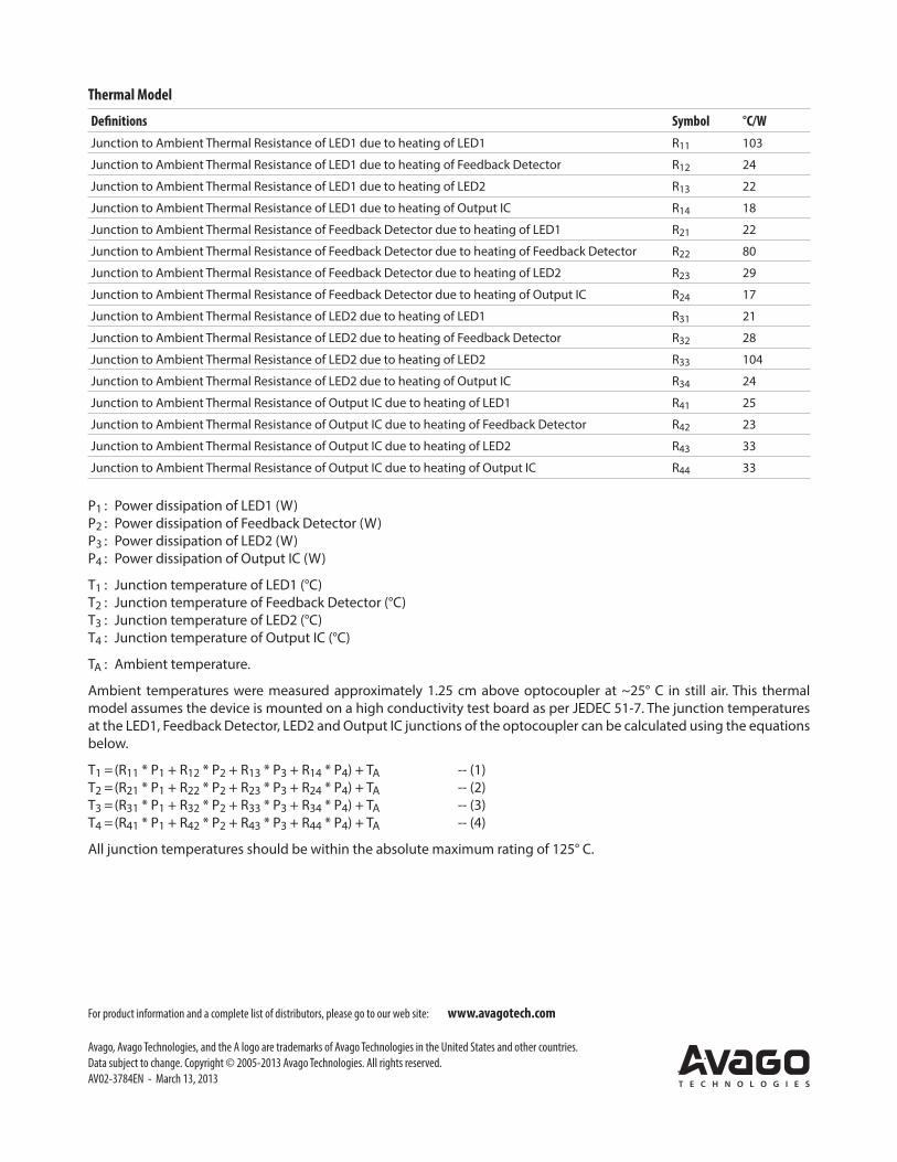
Thermal Model
Definitions Symbol °C/WJunction to Ambient Thermal Resistance of LED1 due to heating of LED1 R11 103
Junction to Ambient Thermal Resistance of LED1 due to heating of Feedback Detector R12 24
Junction to Ambient Thermal Resistance of LED1 due to heating of LED2 R13 22
Junction to Ambient Thermal Resistance of LED1 due to heating of Output IC R14 18
Junction to Ambient Thermal Resistance of Feedback Detector due to heating of LED1 R21 22
Junction to Ambient Thermal Resistance of Feedback Detector due to heating of Feedback Detector R22 80
Junction to Ambient Thermal Resistance of Feedback Detector due to heating of LED2 R23 29
Junction to Ambient Thermal Resistance of Feedback Detector due to heating of Output IC R24 17
Junction to Ambient Thermal Resistance of LED2 due to heating of LED1 R31 21
Junction to Ambient Thermal Resistance of LED2 due to heating of Feedback Detector R32 28
Junction to Ambient Thermal Resistance of LED2 due to heating of LED2 R33 104
Junction to Ambient Thermal Resistance of LED2 due to heating of Output IC R34 24
Junction to Ambient Thermal Resistance of Output IC due to heating of LED1 R41 25
Junction to Ambient Thermal Resistance of Output IC due to heating of Feedback Detector R42 23
Junction to Ambient Thermal Resistance of Output IC due to heating of LED2 R43 33
Junction to Ambient Thermal Resistance of Output IC due to heating of Output IC R44 33
P1 : Power dissipation of LED1 (W) P2 : Power dissipation of Feedback Detector (W) P3 : Power dissipation of LED2 (W) P4 : Power dissipation of Output IC (W)
T1 : Junction temperature of LED1 (°C) T2 : Junction temperature of Feedback Detector (°C) T3 : Junction temperature of LED2 (°C) T4 : Junction temperature of Output IC (°C)
TA : Ambient temperature.
Ambient temperatures were measured approximately 1.25 cm above optocoupler at ~25° C in still air. This thermal model assumes the device is mounted on a high conductivity test board as per JEDEC 51-7. The junction temperatures at the LED1, Feedback Detector, LED2 and Output IC junctions of the optocoupler can be calculated using the equations below.
T1 = (R11 * P1 + R12 * P2 + R13 * P3 + R14 * P4) + TA -- (1) T2 = (R21 * P1 + R22 * P2 + R23 * P3 + R24 * P4) + TA -- (2) T3 = (R31 * P1 + R32 * P2 + R33 * P3 + R34 * P4) + TA -- (3) T4 = (R41 * P1 + R42 * P2 + R43 * P3 + R44 * P4) + TA -- (4)
All junction temperatures should be within the absolute maximum rating of 125° C.