Research Article An Analytical Gate-All-Around MOSFET...
6
Research Article An Analytical Gate-All-Around MOSFET Model for Circuit Simulation Kuan-Chou Lin, 1 Wei-Wen Ding, 2 and Meng-Hsueh Chiang 1 1 MS Degree Program on Nano-IC Engineering, Department of Electrical Engineering, National Cheng Kung University, Tainan 701, Taiwan 2 Department of Electronic Engineering, National Ilan University, I-Lan 260, Taiwan Correspondence should be addressed to Meng-Hsueh Chiang; [email protected] Received 20 September 2014; Accepted 24 November 2014 Academic Editor: Satoshi Horikoshi Copyright © 2015 Kuan-Chou Lin et al. is is an open access article distributed under the Creative Commons Attribution License, which permits unrestricted use, distribution, and reproduction in any medium, provided the original work is properly cited. A generic charge-based compact model for undoped (lightly doped) quadruple-gate (QG) and cylindrical-gate MOSFETs using Verilog-A is developed. is model is based on the exact solution of Poisson’s equation with scale length. e fundamental DC and charging currents of QG MOSFETs are physically and analytically calculated. In addition, as the Verilog-A modeling is portable for different circuit simulators, the modeling scheme provides a useful tool for circuit designers. 1. Introduction According to Moore’s law, CMOS transistors continue to scale. e transistor size scaling provides for increased pack- ing density, improves circuit speed, and lowers power con- sumption. However, many small-geometry effects have sur- faced such as short-channel effects, limiting the device perfor- mance. In order to overcome these issues, improving device gate controllability is necessary. Multigate transistor architec- ture is regarded as one of the most effective ways to improve the short-channel effects and to enhance the gate controllabil- ity [1–3]. e gate-all-around (GAA) MOSFETs have drawn much attention for ultimate device scaling. To expedite fur- ther VLSI development using GAA devices, we use Verilog-A to develop the SPICE device model which can be used by cir- cuit/device designers with a simple set of physical parameters. 2. Potential Model and I-V Model Based on Scale Length We propose a scale-length based GAA MOSFET model. e schematic diagram of the QG MOSFET for modeling is shown in Figure 1. e model is based on an undoped n- channel multigate MOSFET. Unlike most models limited to a certain specific type of the gate, the proposed model is highly scalable and is generic to both quadruple-gate (QG) and cylindrical-gate structures. Poisson’s equation for potential can be written as [4] 1 ( (, ))+ 2 2 (, ) = si , (1) where is the channel doping (assumed to be uniform in the model) and represents any position in the channel [4], which is equivalent to ( × )/( + ) for any specific location (, ) in - plane [5]. e solution for (, ) is (, ) = () −( (2 ox 2 ( () − gs )) ( si 2 si ln (1 + 2 ox / si )+ ox 2 si /2) ), (2) where gs = GS − FB , si = 2 × ( si × si )/( si + si ), and () is the channel center potential, which can be solved at =0 as 2 2 () − (( () − gs )) 2 = si , (3) Hindawi Publishing Corporation Advances in Materials Science and Engineering Volume 2015, Article ID 320320, 5 pages http://dx.doi.org/10.1155/2015/320320
Transcript of Research Article An Analytical Gate-All-Around MOSFET...

Research ArticleAn Analytical Gate-All-Around MOSFET Model forCircuit Simulation
Kuan-Chou Lin,1 Wei-Wen Ding,2 and Meng-Hsueh Chiang1
1MS Degree Program on Nano-IC Engineering, Department of Electrical Engineering,National Cheng Kung University, Tainan 701, Taiwan2Department of Electronic Engineering, National Ilan University, I-Lan 260, Taiwan
Correspondence should be addressed to Meng-Hsueh Chiang; [email protected]
Received 20 September 2014; Accepted 24 November 2014
Academic Editor: Satoshi Horikoshi
Copyright © 2015 Kuan-Chou Lin et al.This is an open access article distributed under the Creative CommonsAttribution License,which permits unrestricted use, distribution, and reproduction in any medium, provided the original work is properly cited.
A generic charge-based compact model for undoped (lightly doped) quadruple-gate (QG) and cylindrical-gate MOSFETs usingVerilog-A is developed.This model is based on the exact solution of Poisson’s equation with scale length.The fundamental DC andcharging currents of QGMOSFETs are physically and analytically calculated. In addition, as the Verilog-Amodeling is portable fordifferent circuit simulators, the modeling scheme provides a useful tool for circuit designers.
1. Introduction
According to Moore’s law, CMOS transistors continue toscale. The transistor size scaling provides for increased pack-ing density, improves circuit speed, and lowers power con-sumption. However, many small-geometry effects have sur-faced such as short-channel effects, limiting the device perfor-mance. In order to overcome these issues, improving devicegate controllability is necessary. Multigate transistor architec-ture is regarded as one of the most effective ways to improvethe short-channel effects and to enhance the gate controllabil-ity [1–3]. The gate-all-around (GAA) MOSFETs have drawnmuch attention for ultimate device scaling. To expedite fur-ther VLSI development using GAA devices, we use Verilog-Ato develop the SPICE device model which can be used by cir-cuit/device designers with a simple set of physical parameters.
2. Potential Model and I-V Model Based onScale Length
We propose a scale-length based GAA MOSFET model. Theschematic diagram of the QG MOSFET for modeling isshown in Figure 1. The model is based on an undoped n-channel multigate MOSFET.
Unlike most models limited to a certain specific type ofthe gate, the proposed model is highly scalable and is genericto both quadruple-gate (QG) and cylindrical-gate structures.Poisson’s equation for potential can be written as [4]
1𝛾
𝜕
𝜕𝛾(𝛾
𝜕
𝜕𝛾𝜙 (𝑟, 𝑦)) +
𝜕2
𝜕𝑧2𝜙 (𝑟, 𝑦) =
𝑞𝑁𝑎
𝜀si, (1)
where 𝑁𝑎is the channel doping (assumed to be uniform in
the model) and 𝑟 represents any position in the channel [4],which is equivalent to (𝑊 × 𝐻)/(𝑊 + 𝐻) for any specificlocation (𝑊,𝐻) in 𝑥-𝑧 plane [5]. The solution for 𝜙(𝑟, 𝑦) is
𝜙 (𝑟, 𝑦) = 𝜙𝑐(𝑦)
−((2𝜀ox𝑟
2(𝜙𝑐(𝑦) − 𝜙gs))
(𝜀si𝑡2si ln (1 + 2𝑡ox/𝑡si) + 𝜀ox𝑡2si/2)
) ,
(2)
where 𝜙gs = 𝑉GS − 𝑉FB, 𝑡si = 2 × (𝑊si × 𝐻si)/(𝑊si + 𝐻si), and𝜙𝑐(𝑦) is the channel center potential, which can be solved at
𝑟 = 0 as
𝜕2
𝜕𝑦2𝜙𝑐(𝑦) −
((𝜙𝑐(𝑦) − 𝜙gs))
𝜆2=𝑞𝑁𝑎
𝜀si, (3)
Hindawi Publishing CorporationAdvances in Materials Science and EngineeringVolume 2015, Article ID 320320, 5 pageshttp://dx.doi.org/10.1155/2015/320320
2 Advances in Materials Science and Engineering
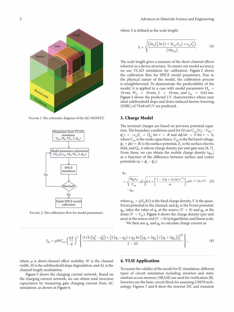
Buried oxideSi substrate
Source
Drain
Gate
Lg
tox
Figure 1: The schematic diagram of the QGMOSFET.
SPICEsimulation
Matched?
No
Finish SPICE modelcalibration
Yes
Model parameters adjustment(Na, 𝜇, tox , Hsi ,Wsi , L, 𝜙m)
Parameters from TCADsimulation
(tox , Hsi ,Wsi , L, 𝜙m)
Figure 2: The calibration flow for model parameters.
where 𝜆 is defined as the scale length:
𝜆 = √(2𝜀si𝑡
2si ln (1 + 2𝑡ox/𝑡si) + 𝜀ox𝑡
2si)
(16𝜀ox). (4)
The scale length gives a measure of the short-channel effectsinherent in a device structure. To ensure our model accuracy,we use TCAD simulation for calibration. Figure 2 showsthe calibration flow for SPICE model parameters. Due tothe physical nature of the model, the calibration processis straightforward. To demonstrate the predictability of themodel, it is applied to a case with model parameters 𝐻si =10 nm, 𝑊si = 10 nm, 𝐿 = 10 nm, and 𝑡ox = 0.62 nm.Figure 3 shows the predicted I-V characteristics where nearideal subthreshold slope and drain-induced barrier lowering(DIBL) of 79.68mV/V are predicted.
3. Charge Model
The terminal charges are based on previous potential equa-tion.The boundary conditions used for (1) are𝐶ox(𝑉𝐺−𝑉FB −𝜙𝑠) = −𝜀si𝐸𝑠 = 𝑄si for 𝑟 = 𝑅 and 𝑑𝜙/𝑑𝑟 = 0 for 𝑟 = 0,
where𝐶ox is the oxide capacitance,𝑉FB is the flat band voltage,𝜙𝑠= 𝜙(𝑟 = 𝑅) is the surface potential,𝐸
𝑠is the surface electric
field, and𝑄si is silicon charge density per unit gate area [6, 7].From them, we can obtain the mobile charge density (𝑞
𝑚)
as a function of the difference between surface and centerpotentials (𝛼 = 𝜙
𝑠− 𝜙𝑐):
𝑞𝑚
= √4𝑞𝑝𝜀si
𝐶ox√𝛼√0.5 + [1 − 1/𝛼 + (1/𝛼) 𝑒−𝛼
𝛼] 𝑒𝑞(𝜙𝑠−𝑉−2𝜙𝐹)/𝑘𝑇
− 𝑞𝑝,
(5)
where 𝑞𝑝= 𝑞𝑁𝑎𝑅/2 is the fixed charge density,𝑉 is the quasi-
Fermi potential in the channel, and 𝜙𝐹is the Fermi potential.
𝑞𝑚takes the value of 𝑞
𝑠at the source (𝑉 = 0) and 𝑞
𝑑at the
drain (𝑉 = 𝑉𝑑𝑠). Figure 4 shows the charge density (per unit
area) at the source end (𝑉 = 0) in logarithmic and linear scale.We then use 𝑞
𝑠and 𝑞𝑑to calculate charge current as
𝐼𝑑𝑠= 𝜇𝑊𝐶ox (
𝑘𝑇
𝑞)
2{{
{
(1/2) (𝑞2𝑠− 𝑞
2𝑑) + [2 (𝑞
𝑠− 𝑞𝑑) + 𝑞𝑝ln ((𝑞
𝑑+ 2𝑞𝑝) / (𝑞𝑠+ 2𝑞𝑝))]
SS
𝐿 − Δ𝐿
}
}
}
, (6)
where 𝜇 is short-channel effect mobility, 𝑊 is the channelwidth, SS is the subthreshold slope degradation, andΔ𝐿 is thechannel length modulation.
Figure 5 shows the charging current network. Based onthe charging current network, we can obtain total inversioncapacitance by measuring gate charging current from ACsimulation, as shown in Figure 6.
4. VLSI Application
To ensure the validity of themodel for IC simulation, differenttypes of circuit simulation including inverters and staticrandom access memory (SRAM) are used for verification [8].Inverters are the basic circuit block for assessing CMOS tech-nology. Figures 7 and 8 show the inverter DC and transient

Advances in Materials Science and Engineering 3
0.0 0.1 0.2 0.3 0.4 0.5 0.6 0.7
10−4
10−5
10−6
10−7
10−8
10−9
Our model by SPICE simulationOur model by SPICE simulation
VGS (V)
3D numerical simulation3D numerical simulation
VDS = 0.68V
VDS = 50mV
I DS
(A)
Figure 3: Simulated drain current as a function of gate voltage atlow and high drain biases.
0.0 0.1 0.2 0.3 0.4 0.5 0.6 0.7
0.030
0.025
0.020
0.015
0.010
0.005
0.000
10−5
10−6
10−7
10−8
10−9
10−10
VGS (V)
Q(C
/m2)
Figure 4: Channel charge density (per unit area) at the source end(𝑉 = 0) in logarithmic and linear scale.
ICH
dQsi/2dt dQsi/2dt
dQsi/dt
RS RD
Gate
DrainSource
Figure 5: Charging current network diagram.
0.0 0.1 0.2 0.3 0.4 0.5 0.6
120
100
80
60
40
20
0
Our model by SPICE simulation3D numerical simulation
VGS (V)
CG
(𝜇F/
cm2)
Figure 6: Total gate capacitance as a function of gate voltageextracted from AC simulation.
0.0 0.1 0.2 0.3 0.4 0.5 0.6 0.7
0.7
0.6
0.5
0.4
0.3
0.2
0.1
Vin (V)
Vou
t(V
)
Figure 7: DC simulated inverter transfer curve.
0 5 10 15 20
0.7
0.6
0.5
0.4
0.3
0.2
0.1
0.0
−0.1
Time (ps)
Vou
t(V
)
Figure 8: Transient simulated inverter response.
4 Advances in Materials Science and Engineering
WL
BL
M2
M1 M4
M5M3
Vn
Vn
VDD
BLB
M6
Inverter 1 Inverter 2
+ −+ −
Figure 9: Conventional 6T SRAM.
ReadHold
VDD
VDD00
Q (V)
QB
(V)
Figure 10: Read and hold SNMs [9].
simulation using the GAA model, from which the intrinsicinverter speed can be extracted. The circuit simulation givesan insight to device performance very efficiently based on thephysical DC I-V and charge models.
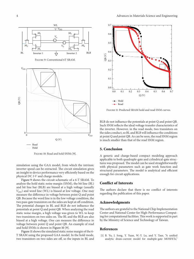
Figure 9 shows the circuit schematic of a 6-T SRAM. Toanalyze the hold static noise margin (SNM), the bit line (BL)and bit line bar (BLB) are biased at a high voltage (usually𝑉DD) and word line (WL) is biased at low voltage. One maymeasure the difference in voltage between point Q and pointQB. Because the word line is in the low voltage condition, thetwo pass-gate transistors on the sides are kept at off condition.The potential changes in BL and BLB do not influence thepotentials at point Q and point QB. When analyzing the readstatic noise margin, a high voltage was given to WL to keeptwo transistors on two sides on. The BL and the BLB are alsobiased at a high voltage. One can measure the difference involtage between point Q and point QB. An example of readand hold SNMs is shown in Figure 10 [9].
Figure 11 shows the simulated static noisemargin of the 6-T SRAM using the proposed GAA model. In the hold mode,two transistors on two sides are off, so the inputs in BL and
ReadHold
0.7
0.6
0.5
0.4
0.3
0.2
0.1
0.0
0.0 0.1 0.2 0.3 0.4 0.5 0.6 0.7
Q (V)
QB
(V)
Figure 11: Predicted SRAM hold and read SNM curves.
BLB do not influence the potentials at point Q and point QB.Such SNM reflects the ideal voltage transfer characteristics ofthe inverter. However, in the read mode, two transistors onthe sides conduct, so BL andBLBwill influence the conditionsat point Q and point QB. As can be seen, the read SNM regionis much smaller than that of the read SNM region.
5. Conclusion
A generic and charge-based compact modeling approachapplicable to both quadruple-gate and cylindrical-gate struc-tures was proposed.Themodel can be used straightforwardlywith physical parameters such as gate work function andstructural parameters. The model is analytical and efficientenough for circuit applications.
Conflict of Interests
The authors declare that there is no conflict of interestsregarding the publication of this paper.
Acknowledgments
Theauthors are grateful to theNational Chip ImplementationCenter and National Center for High-Performance Comput-ing for computational facilities.Thiswork is supported in partby the Ministry of Science and Technology of Taiwan.
References
[1] B. Yu, J. Song, Y. Yuan, W.-Y. Lu, and Y. Taur, “A unifiedanalytic drain-current model for multiple-gate MOSFETs,”

Advances in Materials Science and Engineering 5
IEEE Transactions on Electron Devices, vol. 55, no. 8, pp. 2157–2163, 2008.
[2] J. Song, B. Yu, Y. Yuan, and Y. Taur, “A review on compactmodeling of multiple-gate MOSFETs,” IEEE Transactions onCircuits and Systems. I: Regular Papers, vol. 56, no. 8, pp. 1858–1869, 2009.
[3] J. P. Duarte, S.-J. Choi, D.-I.Moon et al., “A universal coremodelfor multiple-gate field-effect transistors. Part I: charge model,”IEEE Transactions on Electron Devices, vol. 60, no. 2, pp. 840–847, 2013.
[4] C. P. Auth and J. D. Plummer, “Scaling theory for cylindrical,fully-depleted, surrounding-gate MOSFET’s,” IEEE ElectronDevice Letters, vol. 18, no. 2, pp. 74–76, 1997.
[5] N. Chevillon, J.-M. Sallese, C. Lallement et al., “Generalizationof the concept of equivalent thickness and capacitance tomultigate MOSFETs modeling,” IEEE Transactions on ElectronDevices, vol. 59, no. 1, pp. 60–71, 2012.
[6] B. Inıguez, D. Jimenez, J. Roig, H. A. Hamid, L. F. Marsal, and J.Pallares, “Explicit continuous model for long-channel undopedsurrounding gate MOSFETs,” IEEE Transactions on ElectronDevices, vol. 52, no. 8, pp. 1868–1873, 2005.
[7] B. Smaani, S. Latreche, and B. Iniguez, “Compact drain-currentmodel for undoped cylindrical surrounding-gate metal-oxide-semiconductor field effect transistors including short channeleffects,” Journal of Applied Physics, vol. 114, no. 22, Article ID224507, 2013.
[8] B. Calhoun and A. Chandrakasan, “A 256 kb sub-thresholdSRAM in 65 nm CMOS,” in Proceedings of the IEEE Interna-tional Solid-State Circuits Conference, pp. 628–629, 2008.
[9] M. Zamani, S. Hassanzadeh, K. Hajsadeghi, and R. Saeidi,“A 32kb 90nm 9T-cell sub-threshold SRAM with improvedread and write SNM,” in Proceedings of the 8th InternationalConference on Design and Technology of Integrated Systems inNanoscale Era, pp. 104–107, March 2013.

Submit your manuscripts athttp://www.hindawi.com
ScientificaHindawi Publishing Corporationhttp://www.hindawi.com Volume 2014
CorrosionInternational Journal of
Hindawi Publishing Corporationhttp://www.hindawi.com Volume 2014
Polymer ScienceInternational Journal of
Hindawi Publishing Corporationhttp://www.hindawi.com Volume 2014
Hindawi Publishing Corporationhttp://www.hindawi.com Volume 2014
CeramicsJournal of
Hindawi Publishing Corporationhttp://www.hindawi.com Volume 2014
CompositesJournal of
NanoparticlesJournal of
Hindawi Publishing Corporationhttp://www.hindawi.com Volume 2014
Hindawi Publishing Corporationhttp://www.hindawi.com Volume 2014
International Journal of
Biomaterials
Hindawi Publishing Corporationhttp://www.hindawi.com Volume 2014
NanoscienceJournal of
TextilesHindawi Publishing Corporation http://www.hindawi.com Volume 2014
Journal of
NanotechnologyHindawi Publishing Corporationhttp://www.hindawi.com Volume 2014
Journal of
CrystallographyJournal of
Hindawi Publishing Corporationhttp://www.hindawi.com Volume 2014
The Scientific World JournalHindawi Publishing Corporation http://www.hindawi.com Volume 2014
Hindawi Publishing Corporationhttp://www.hindawi.com Volume 2014
CoatingsJournal of
Advances in
Materials Science and EngineeringHindawi Publishing Corporationhttp://www.hindawi.com Volume 2014
Smart Materials Research
Hindawi Publishing Corporationhttp://www.hindawi.com Volume 2014
Hindawi Publishing Corporationhttp://www.hindawi.com Volume 2014
MetallurgyJournal of
Hindawi Publishing Corporationhttp://www.hindawi.com Volume 2014
BioMed Research International
MaterialsJournal of
Hindawi Publishing Corporationhttp://www.hindawi.com Volume 2014
Nano
materials
Hindawi Publishing Corporationhttp://www.hindawi.com Volume 2014
Journal ofNanomaterials