A Review on Modeling the Channel Potential in Multi-Gate ... Hossein Mohammadi.pdf · A Review on...
6
Sains Malaysiana 43(6)(2014): 861–866 A Review on Modeling the Channel Potential in Multi-Gate MOSFETs (Ulasan Terhadap Model Keupayaan Saluran dalam Multi-Gate MOSFET) HOSSEIN MOHAMMADI*, HUDA ABDULLAH & CHANG FU DEE ABSTRACT This paper attempts to give a detailed review and provide a complete description on the technology, physics and modeling of various Multi-Gate MOSFETs. It consists of a synopsis of mathematical depiction of the potential distribution along the channel of various MG-MOSFETs which can be made to enable fast computer analysis of device behavior. This serves a link between process technology and circuit design. This review demonstrates that this technology is strongly desired in nanoscale domain and there is a plenty demand for analytical model which can explain the physics and operation of the devices perfectly. Keywords: Multi-gate SOI MOSFETs; natural channel length; potential distribution; short channel effects ABSTRAK Kertas ini bertujuan untuk memberikan kajian secara terperinci dan memberi penerangan yang lengkap terhadap bidang teknologi, fizik dan model pelbagai berbilang-gerbang MOSFET. Kertas ini merangkumi sinopsis gambaran matematik terhadap pengagihan potensi di sepanjang saluran pelbagai Multi Gate -MOSFET yang boleh menghasilkan sifat peranti untuk analisis komputer berkelajuan tinggi. Hubungan ini menyediakan teknologi proses dan reka bentuk litar. Ulasan ini menunjukkan bahawa teknologi berbilang-gerbang MOSFET amat diperlukan dalam domain berskala nano. Terdapat banyak juga permintaan untuk model analitikal dan ulasan ini boleh menerangkan secara jelas berkenaan fizik dan operasi peranti tersebut. Kata kunci: Berbilang-gerbang SOI MOSFETs; kesan alur; keupayaan agihan; panjang alur asli INTRODUCTION The motivation behind the microelectronic industry development has been the unique scaling ability of CMOS technology. Since the technology advances, the sizes of electronic components are reduced continuously to shrink the device geometry because of the need to accommodate more transistors on a single chip. As transistors dimension penetrate into the sub-micrometer territory, short channel effects (SCEs) become very detrimental to normal operation of device. In order to suppress this undesired phenomenon, it is necessary to reduce the gate oxide thickness and increase channel doping concentration but the use of a thinner gate oxide increases the capacitance between gate and channel. A higher channel doping concentration reduces charge sharing between the gate and drain in the channel, and it creates a large potential barrier between source and drain (Frank & Taur 1998; Xiong 2008). Consequently, it is obvious that the scaling trend, which is just often based on degrading the physical size, has become more challenging and cannot remain anymore. Based on the International Technology Roadmap for Semiconductors (ITRS) for every new device generation, at least one new main material or new device structure must be emerged. Consequently, a variety of non-classical devices have been proposed to extend the scalability of devices as far as possible. Multiple-Gate ( MG) such as double, triple and quadruple Gate SOI MOSFETs are a desired candidate to follow the scaling trend of conventional bulk MOSFETs in nanoscale territory, due to their high current driving capability and excellent suppressing of short-channel effects. The superiority of these devices comes from the better control of the channel and carrier confinement enabled by the association of the multiple gates. MG- MOSFETs have been contemplated in high-performance circuits due to these properties. Because various types of MG-MOSFETs have been proposed and investigated, it is attractive to develop an analytical, accurate and efficient model covering all MG structures (Jooyoung & Bo 2009). We begin our analysis from single gate MOSFET and then extend it to Double-gate and Triple-gate. The structure and advantages of these devices will be described. Then the potential distribution along the channel of these devices will be studied and modeled. SINGLE-GATE SOI MOSFET Structure Single-gate SOI MOSFETs have been found more useful over their bulk counterparts due to their excellent advantages. These devices are known to have suppressed short-channel effects, lower parasitic capacitances and a higher packing density. The operation of these devices is
Transcript of A Review on Modeling the Channel Potential in Multi-Gate ... Hossein Mohammadi.pdf · A Review on...

Sains Malaysiana 43(6)(2014): 861–866
A Review on Modeling the Channel Potential in Multi-Gate MOSFETs(Ulasan Terhadap Model Keupayaan Saluran dalam Multi-Gate MOSFET)
HOSSEIN MOHAMMADI*, HUDA ABDULLAH & CHANG FU DEE
ABSTRACT
This paper attempts to give a detailed review and provide a complete description on the technology, physics and modeling of various Multi-Gate MOSFETs. It consists of a synopsis of mathematical depiction of the potential distribution along the channel of various MG-MOSFETs which can be made to enable fast computer analysis of device behavior. This serves a link between process technology and circuit design. This review demonstrates that this technology is strongly desired in nanoscale domain and there is a plenty demand for analytical model which can explain the physics and operation of the devices perfectly.
Keywords: Multi-gate SOI MOSFETs; natural channel length; potential distribution; short channel effects
ABSTRAK
Kertas ini bertujuan untuk memberikan kajian secara terperinci dan memberi penerangan yang lengkap terhadap bidang teknologi, fizik dan model pelbagai berbilang-gerbang MOSFET. Kertas ini merangkumi sinopsis gambaran matematik terhadap pengagihan potensi di sepanjang saluran pelbagai Multi Gate -MOSFET yang boleh menghasilkan sifat peranti untuk analisis komputer berkelajuan tinggi. Hubungan ini menyediakan teknologi proses dan reka bentuk litar. Ulasan ini menunjukkan bahawa teknologi berbilang-gerbang MOSFET amat diperlukan dalam domain berskala nano. Terdapat banyak juga permintaan untuk model analitikal dan ulasan ini boleh menerangkan secara jelas berkenaan fizik dan operasi peranti tersebut.
Kata kunci: Berbilang-gerbang SOI MOSFETs; kesan alur; keupayaan agihan; panjang alur asli
INTRODUCTION
The motivation behind the microelectronic industry development has been the unique scaling ability of CMOS technology. Since the technology advances, the sizes of electronic components are reduced continuously to shrink the device geometry because of the need to accommodate more transistors on a single chip. As transistors dimension penetrate into the sub-micrometer territory, short channel effects (SCEs) become very detrimental to normal operation of device. In order to suppress this undesired phenomenon, it is necessary to reduce the gate oxide thickness and increase channel doping concentration but the use of a thinner gate oxide increases the capacitance between gate and channel. A higher channel doping concentration reduces charge sharing between the gate and drain in the channel, and it creates a large potential barrier between source and drain (Frank & Taur 1998; Xiong 2008). Consequently, it is obvious that the scaling trend, which is just often based on degrading the physical size, has become more challenging and cannot remain anymore. Based on the International Technology Roadmap for Semiconductors (ITRS) for every new device generation, at least one new main material or new device structure must be emerged. Consequently, a variety of non-classical devices have been proposed to extend the scalability of devices as far as possible.
Multiple-Gate (MG) such as double, triple and quadruple Gate SOI MOSFETs are a desired candidate to follow the scaling trend of conventional bulk MOSFETs in nanoscale territory, due to their high current driving capability and excellent suppressing of short-channel effects. The superiority of these devices comes from the better control of the channel and carrier confinement enabled by the association of the multiple gates. MG-MOSFETs have been contemplated in high-performance circuits due to these properties. Because various types of MG-MOSFETs have been proposed and investigated, it is attractive to develop an analytical, accurate and efficient model covering all MG structures (Jooyoung & Bo 2009).We begin our analysis from single gate MOSFET and then extend it to Double-gate and Triple-gate. The structure and advantages of these devices will be described. Then the potential distribution along the channel of these devices will be studied and modeled.
SINGLE-GATE SOI MOSFET
Structure Single-gate SOI MOSFETs have been found more useful over their bulk counterparts due to their excellent advantages. These devices are known to have suppressed short-channel effects, lower parasitic capacitances and a higher packing density. The operation of these devices is

862
generally separated into two distinct regimes of the fully depleted (FD) and the partially depleted (PD) Si film. The operating mode relies on the applied bias, the channel doping concentration and the film thickness (Yu & Kim 2005). Figure 1 shows a typical schematic cross-sectional view of a fully depleted SOI MOSFET.
where tf and tb denote the gate oxide and buried oxide thickness, respectively; εox is the dielectric constant of oxide; Vbi is the built-in potential across the source-drain channel junctions; VGS and VSUB are gate bias and substrate bias, respectively. Also Vfb,f and Vfb,b are the flat band voltage between the channel and the oxide layers (front oxide and back oxide). The first and the second boundary condition address the surface potential along the interface of two oxide layers/silicon film while two next boundary conditions arises from the continuity of the electric flux at the interface of gate/front oxide and buried oxide/silicon film, respectively (Imam & Osman 1993). In this case the electric field at y = tSi is negligible so we set it at zero. By defining γ = εsi/εox and jGS = VGS – VFB and setting the boundary conditions in Eq. (2), the coefficients c0(x), c1(x) and c2(x) can be deduced. Consequently, (2) becomes the following expression in which the function φf(x) is to be solved,
j(x,y) = jf (x) – (4)
By using (4) and (1) and setting y=0, we obtain,
(5)
Equation (5) can be transformed to the second-order 1D differential equation by considering j(x) = jf (x) – jGS + thus we have:
(6)
The parameter is called natural channel length which describes the short channel effects in the device, considering that the current flows along the channel. Equation (6) can be uniquely solved by considering two boundary conditions which are the potentials at the source (x = 0) and the drain (x = L)
jSource = j(x = 0) = Vbi – jGS + ,
jDrain = j(x = L) = VDS + Vbi – jGS + . (7)
Solving (6) using (9) and (10) yields
(8)
FIGURE 1. Cross-sectional view of a fully depleted SOI MOSFET
Model Derivation Generally the potential distribution profile in the semiconductor body, φ(x,y), is governed by the Poisson’s equation (Suzuki & Pidin 2003). This is given by:
0 ≤ x ≤ L and 0 ≤ y ≤ tsi,
(1)
where NA denotes the acceptor doping concentration, εsi is the permittivity of silicon, tsi is silicon film thickness and L is device channel length. Also x and y represent the parallel and perpendicular directions to the channel, respectively.According to the Young’s method (Young 1989) the potential profile in the vertical direction can be approximated by a simple parabolic function which gives an expression of the form,
j(x,y) = c0(x) +c1(x)y + c2(x)y2, (2)
where the coefficients c0(x), c1(x) and c2(x) are depended on x only. To define these coefficients the Poisson’s equation should be solved using the proper set of boundary conditions as follows[Imam, 1993 #1]{Imam, 1993 #1}{Imam, 1993 #1}:
j(x,0) = jf (x), j(x, tsi) = jb(x)
(3)

863
DOUBLE-GATE SOI MOSFET
Structure The double-gate MOS transistor has been introduced for the first time by Sekigawa and Hayashi (1984). They evinced that one can obtain considerable reduction of short-channel effects by sandwiching a fully depleted SOI device between two gate electrodes connected together. Using this structure, as shown in Figure 2, a better control of the channel depletion region was achieved and the influence of the drain electric field on the channel was reduced. This means that a short-channel effect was diminished, than in a normal SOI MOSFET. Another important attribute of double-gate MOSFETs is volume inversion which appears in very thin film multi-gate SOI MOSFETs due to the fact that inversion carriers are not confined near the Si/SiO2 interface, as predicted by conventional device physics, but rather at the centre of the film (Colinge 2008).
β = (10)
By using boundary conditions as
and
the potential distribution along the channel at the front and the back gate interfaces is obtained as following:
(11)
where and (12)
To find a two dimensional function for potential distribution, we need to find the relation between φs(x) and the potential φy(x) at a depth y corresponding to a fraction n of the silicon thickness. Setting x=tsi/n in (2) yields,
where and
(13)
By substituting (13) in (1), we found the following differential equation.
where
and (14)
Equation (14) can be solved by using and and the two-dimensional function for potential distribution along the channel is obtained as follows:
(15)
where:
and
FIGURE 2. Cross-sectional view of a symmetric double-gate MOSFET
Model Derivation In this structure, electrostatic potential φ in the silicon film accords the Poisson’s equation same as single-gate model and (1) is still valid. The boundary conditions in which the continuity of the potential distribution and electric field at the interface of two oxide layers/silicon film (y=0 and y=tsi) are used (Mohammadi et al. 2011). They are given as:
j(x,0) = j(x,tsi) = js(x),
(9)
where tsi and tox are the silicon film thickness and oxide thickness, respectively. Using the same parabolic potential profile in y direction, same as single gate MOSFET and applying the above boundary conditions the arbitrary constants c0(x)-c2(x) can then be determined (Tsormpatzoglou & Dimitriadis 2007) and (1) becomes:
with

864
(16)
Here λ2 is the natural length having the same physical meaning as λ1 and represents the distance of penetration of the drain electric field in the channel.
TRIPLE-GATE SOI MOSFET
Structure The triple-gate MOSFET is a thin-film, narrow silicon island with a gate that is folded over three sides of the transistor (Lemme et al. 2003). In this structure a substrate region made of silicon with a thick layer of Buried Oxide (BOX), which is placed on the substrate, is used. The source, drain, channel and the gate regions of the device are located on the BOX layer. In other words, the inactive channel region is isolated from the substrate by the buried oxide (BOX) layer to improve the substrate noise (Nirmal & Joy 2012). Due to the presence of the additional lateral gates, the effective gate control of the fin and of the buried oxide (BOX) enhances which reduces DIBL. Also to reduce the mobility degradation, the very lightly doped, or undoped channel is used. Triple-Gate fully depleted transistors can be fabricated with various body dimensions which were flexible and relaxed compared to single-gate or double-gate devices (Doyle & Boyanov 2003). A typical schematic view of three dimensional Triple-gate is shown in Figure 3.
Model Derivation It has been demonstrated that the potential distribution of a surrounding-gate MOSFET can
be found by separating the device into a cylindrical gate MOSFET and a symmetric DG MOSFET (Auth & Plummer 1998) as shown in Figure 4.
For triple-gate devices such that (1) extends
to three-dimensional form. It has been demonstrated that the potential distribution of this device, j(x,y,z), can be considered as a perimeter-weighted sum of the ja(x,y) and js(y,z), where ja and js are the potential distribution of the cylindrical and the symmetric DG MOSFET, respectively (Auth & Plummer 1998). The boundary conditions to (1) are:
and
(17)
Using the same approach, to the previous step, the surface potential of the asymmetric and symmetric DG MOSFETs is obtained as:
(18)
where,
(19)
FIGURE 3. The structure of Triple gate MOSFET
FIGURE 4. Triple-gate separation into two devices
865
Now we use the factor R=W/(W+tsi) to have the perimeter-weighted sum of the two potential distribution (Auth & Plummer 1998):
(20)
RESULTS
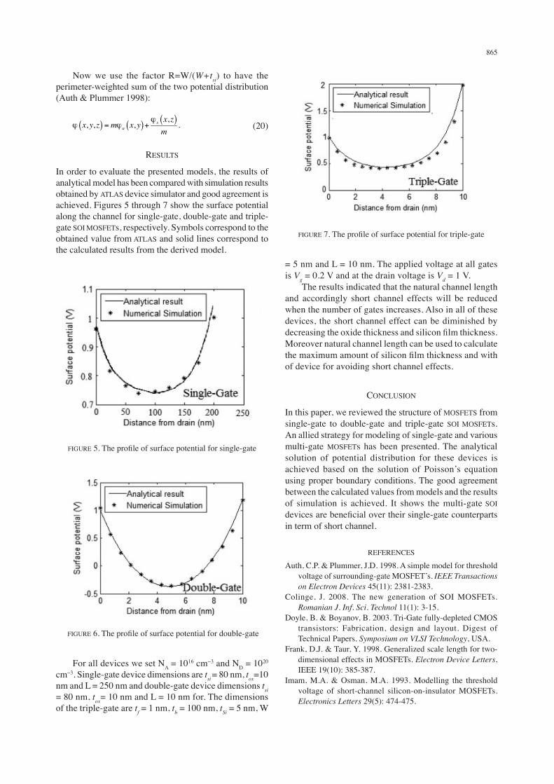
In order to evaluate the presented models, the results of analytical model has been compared with simulation results obtained by ATLAS device simulator and good agreement is achieved. Figures 5 through 7 show the surface potential along the channel for single-gate, double-gate and triple-gate SOI MOSFETs, respectively. Symbols correspond to the obtained value from ATLAS and solid lines correspond to the calculated results from the derived model.
= 5 nm and L = 10 nm. The applied voltage at all gates is Vg = 0.2 V and at the drain voltage is Vd = 1 V. The results indicated that the natural channel length and accordingly short channel effects will be reduced when the number of gates increases. Also in all of these devices, the short channel effect can be diminished by decreasing the oxide thickness and silicon film thickness. Moreover natural channel length can be used to calculate the maximum amount of silicon film thickness and with of device for avoiding short channel effects.
CONCLUSION
In this paper, we reviewed the structure of MOSFETS from single-gate to double-gate and triple-gate SOI MOSFETs. An allied strategy for modeling of single-gate and various multi-gate MOSFETs has been presented. The analytical solution of potential distribution for these devices is achieved based on the solution of Poisson’s equation using proper boundary conditions. The good agreement between the calculated values from models and the results of simulation is achieved. It shows the multi-gate SOI devices are beneficial over their single-gate counterparts in term of short channel.
REFERENCES
Auth, C.P. & Plummer, J.D. 1998. A simple model for threshold voltage of surrounding-gate MOSFET’s. IEEE Transactions on Electron Devices 45(11): 2381-2383.
Colinge, J. 2008. The new generation of SOI MOSFETs. Romanian J. Inf. Sci. Technol 11(1): 3-15.
Doyle, B. & Boyanov, B. 2003. Tri-Gate fully-depleted CMOS transistors: Fabrication, design and layout. Digest of Technical Papers. Symposium on VLSI Technology, USA.
Frank, D.J. & Taur, Y. 1998. Generalized scale length for two-dimensional effects in MOSFETs. Electron Device Letters, IEEE 19(10): 385-387.
Imam, M.A. & Osman, M.A. 1993. Modelling the threshold voltage of short-channel silicon-on-insulator MOSFETs. Electronics Letters 29(5): 474-475.
FIGURE 5. The profile of surface potential for single-gate
FIGURE 6. The profile of surface potential for double-gate
For all devices we set NA = 1016 cm−3 and ND = 1020 cm−3. Single-gate device dimensions are tsi = 80 nm, tox=10 nm and L = 250 nm and double-gate device dimensions tsi = 80 nm, tox= 10 nm and L = 10 nm for. The dimensions of the triple-gate are tf = 1 nm, tb = 100 nm, tSi = 5 nm, W
FIGURE 7. The profile of surface potential for triple-gate

866
Jooyoung, S. & Bo, Y. 2009. A review on compact modeling of multiple-gate MOSFETs. Circuits and Systems I: Regular Papers. IEEE Transactions on Electron Devices 56(8): 1858-1869.
Lemme, M., Mollenhauer, T., Henschel, W., Wahlbrink, T., Gottlob, H., Efavi, J., Baus, M., Winkler, O., Spangenberg, B. & Kurz, H. 2003. Subthreshold behavior of triple-gate MOSFETs on SOI Material. Solid State Electronics Letters 48(4): 529-534.
Mohammadi, H., Abdullah, H., Dee, C.F., Menon, S. & Majlis, B.Y. 2011. A new analytical model for lateral breakdown voltage of double-gate power MOSFETs. 2011 IEEE Regional Symposium on Micro and Nanoelectronics (RSM).
Nirmal, D. & Joy, D. 2012. Low power analysis of Triple Gate MOSFETs. 2012 International Conference on Devices, Circuits and Systems (ICDCS), India.
Sekigawa, T. & Hayashi, Y. 1984. Calculated threshold-voltage characteristics of an XMOS transistor having an additional bottom gate. Solid-State Electronics 27(8): 827-828.
Suzuki, K. & Pidin, S. 2003. Short-channel single-gate SOI MOSFET model. IEEE Transactions on Electron Devices 50(5): 1297-1305.
Tsormpatzoglou, A. & Dimitriadis, C.A. 2007. Semi-analytical modeling of short-channel effects in Si and Ge symmetrical double-gate MOSFETs. IEEE Transactions on Electron Devices 54(8): 1943-1952.
Xiong, W.W. 2008. Multigate MOSFET Technology. In FinFETs and Other Multi-Gate Transistors, edited by Colinge, J-P. New York: Springer.
Young, K.K. 1989. Short-channel effect in fully depleted SOI MOSFETs. IEEE Transactions on Electron Devices 36(2): 399-402.
Yu, Y.S. & Kim, S.H. 2005. All-analytic surface potential model for SOI MOSFETs. Circuits, Devices and Systems, IEE Proceedings 152(2): 183-188.
Hossein Mohammadi* & Huda Abdullah Department of Electrical, Electronic and Systems EngineeringFaculty of EngineeringUniversiti Kebangsaan Malaysia 43600 UKM Bangi, SelangorMalaysia
Chang Fu DeeInstitute of Microengineering and Nanoelectronics (IMEN)Universiti Kebangsaan Malaysia 43600 UKM Bangi, SelangorMalaysia
*Corresponding author; email: [email protected]
Received: 25 April 2013Accepted: 23 January 2014