UCC5350-Q1 Single-Channel Isolated Gate Driver ... - ti.com
41
text VCC2 UVLO, Level Shift and Control Logic VCC2 OUT IN– IN+ CLAMP VCC1 VEE2 GND1 ISOLATION BARRIER UVLO and Input Logic 13.2V – 33V Rest of Circuit 3V – 15V 2V Product Folder Order Now Technical Documents Tools & Software Support & Community An IMPORTANT NOTICE at the end of this data sheet addresses availability, warranty, changes, use in safety-critical applications, intellectual property matters and other important disclaimers. PRODUCTION DATA. UCC5350-Q1 SLUSE29B – MAY 2020 – REVISED JUNE 2020 UCC5350-Q1 Single-Channel Isolated Gate Driver for SiC/IGBT and Automotive Applications 1 1 Features 1• 5-kV RMS and 3-kV RMS single-channel isolated gate driver • AEC-Q100 qualified for automotive applications – Temperature grade 1 – HBM ESD classification level H2 – CDM ESD classification level C6 • ±5-A minimum peak current drive strength • 3-V to 15-V input supply voltage • Up to 33-V driver supply voltage • 100-V/ns minimum CMTI • Negative 5-V handling capability on input pins • 100-ns (maximum) propagation delay and <25ns part-to-part skew • 12-V UVLO • 8-pin DWV (8.5mm creepage) and D (4-mm creepage) packages • Isolation barrier life > 40 Years • Safety-related certifications: – 7000-V PK isolation DWV and 4242-V PK isolation D per DIN V VDE V 0884-11:2017-01 and DIN EN 61010-1 (planned) – 5000-V RMS DWV and 3000-V RMS D isolation rating for 1 minute per UL 1577 (planned) – CQC certification per GB4943.1-2011 D and DWV (planned) • CMOS inputs • Operating junction temperature: –40°C to +150°C 2 Applications • On-board charger • Traction inverter for EVs • DC charging stations • HVAC • Heaters 3 Description The UCC5350-Q1 is a single-channel, isolated gate driver with 5-A source and 5-A sink minimum peak current designed to drive MOSFETs, IGBTs, and SiC MOSFETs. The UCC5350-Q1 has a CLAMP pin to connect the transistor gate to an internal clamp to prevent false turn-on caused by Miller current. The UCC5350-Q1 is available in a 4 mm SOIC-8 (D) or 8.5 mm wide body SOIC-8 (DWV) package and can support isolation voltage up to 3-kV RMS and 5- kV RMS , respectively. The input side is isolated from the output side with SiO2 capacitive isolation technology with longer than 40 years isolation barrier lifetime. The UCC5350-Q1 is a good fit for driving IGBTs or MOSFETs in applications such as high- voltage traction inverters and on-board chargers. Compared to an optocoupler, the UCC5350-Q1 has lower part-to-part skew, lower propagation delay, higher operating temperature, and higher CMTI. Device Information (1) PART NUMBER PACKAGE BODY SIZE (NOM) UCC5350-Q1 DWV SOIC-8 7.5 mm × 5.85 mm D SOIC-8 3.91 mm x 4.9 mm (1) For all available packages, see the orderable addendum at the end of the data sheet. Functional Block Diagram
Transcript of UCC5350-Q1 Single-Channel Isolated Gate Driver ... - ti.com
text
VCC2
UVLO, LevelShiftand
ControlLogic
VCC2
OUT
IN±�
IN+
CLAMP
VCC1
VEE2GND1
ISO
LA
TIO
N
BA
RR
IER
UVLO and Input Logic
13.2V ±�33V
Rest of Circuit
3V ±�15V
2V
Product
Folder
Order
Now
Technical
Documents
Tools &
Software
Support &Community
An IMPORTANT NOTICE at the end of this data sheet addresses availability, warranty, changes, use in safety-critical applications,intellectual property matters and other important disclaimers. PRODUCTION DATA.
UCC5350-Q1SLUSE29B –MAY 2020–REVISED JUNE 2020
UCC5350-Q1 Single-Channel Isolated Gate Driverfor SiC/IGBT and Automotive Applications
1
1 Features1• 5-kVRMS and 3-kVRMS single-channel isolated gate
driver• AEC-Q100 qualified for automotive applications
– Temperature grade 1– HBM ESD classification level H2– CDM ESD classification level C6
• ±5-A minimum peak current drive strength• 3-V to 15-V input supply voltage• Up to 33-V driver supply voltage• 100-V/ns minimum CMTI• Negative 5-V handling capability on input pins• 100-ns (maximum) propagation delay and <25ns
part-to-part skew• 12-V UVLO• 8-pin DWV (8.5mm creepage)
and D (4-mm creepage) packages• Isolation barrier life > 40 Years• Safety-related certifications:
– 7000-VPK isolation DWV and 4242-VPKisolation D per DIN V VDE V 0884-11:2017-01and DIN EN 61010-1 (planned)
– 5000-VRMS DWV and 3000-VRMS Disolation rating for 1 minute per UL 1577(planned)
– CQC certification per GB4943.1-2011D and DWV (planned)
• CMOS inputs• Operating junction temperature: –40°C to +150°C
2 Applications• On-board charger• Traction inverter for EVs• DC charging stations• HVAC• Heaters
3 DescriptionThe UCC5350-Q1 is a single-channel, isolated gatedriver with 5-A source and 5-A sink minimum peakcurrent designed to drive MOSFETs, IGBTs, and SiCMOSFETs. The UCC5350-Q1 has a CLAMP pin toconnect the transistor gate to an internal clamp toprevent false turn-on caused by Miller current.
The UCC5350-Q1 is available in a 4 mm SOIC-8 (D)or 8.5 mm wide body SOIC-8 (DWV) package andcan support isolation voltage up to 3-kVRMS and 5-kVRMS, respectively. The input side is isolated fromthe output side with SiO2 capacitive isolationtechnology with longer than 40 years isolation barrierlifetime. The UCC5350-Q1 is a good fit for drivingIGBTs or MOSFETs in applications such as high-voltage traction inverters and on-board chargers.
Compared to an optocoupler, the UCC5350-Q1 haslower part-to-part skew, lower propagation delay,higher operating temperature, and higher CMTI.
Device Information(1)
PART NUMBER PACKAGE BODY SIZE (NOM)
UCC5350-Q1DWV SOIC-8 7.5 mm × 5.85 mm
D SOIC-8 3.91 mm x 4.9 mm
(1) For all available packages, see the orderable addendum atthe end of the data sheet.
Functional Block Diagram
2
UCC5350-Q1SLUSE29B –MAY 2020–REVISED JUNE 2020 www.ti.com
Product Folder Links: UCC5350-Q1
Submit Documentation Feedback Copyright © 2020, Texas Instruments Incorporated
Table of Contents1 Features .................................................................. 12 Applications ........................................................... 13 Description ............................................................. 14 Revision History..................................................... 25 Pin Configuration and Function ........................... 36 Specifications......................................................... 4
6.1 Absolute Maximum Ratings ...................................... 46.2 ESD Ratings.............................................................. 46.3 Recommended Operating Conditions....................... 46.4 Thermal Information .................................................. 56.5 Power Ratings........................................................... 56.6 Insulation Specifications for D Package.................... 66.7 Insulation Specifications for DWV Package.............. 76.8 Safety-Related Certifications For D Package ........... 86.9 Safety-Related Certifications For DWV Package...... 86.10 Safety Limiting Values ............................................ 86.11 Electrical Characteristics......................................... 96.12 Switching Characteristics ...................................... 106.13 Insulation Characteristics Curves ......................... 106.14 Typical Characteristics .......................................... 11
7 Parameter Measurement Information ................ 147.1 Propagation Delay, Inverting, and Noninverting
Configuration............................................................ 14
8 Detailed Description ............................................ 168.1 Overview ................................................................. 168.2 Functional Block Diagram ....................................... 168.3 Feature Description................................................. 178.4 Device Functional Modes........................................ 20
9 Application and Implementation ........................ 229.1 Application Information............................................ 229.2 Typical Application ................................................. 22
10 Power Supply Recommendations ..................... 2711 Layout................................................................... 28
11.1 Layout Guidelines ................................................. 2811.2 Layout Example .................................................... 2911.3 PCB Material ......................................................... 31
12 Device and Documentation Support ................. 3212.1 Documentation Support ........................................ 3212.2 Certifications ......................................................... 3212.3 Related Links ........................................................ 3212.4 Receiving Notification of Documentation Updates 3212.5 Community Resources.......................................... 3212.6 Trademarks ........................................................... 3212.7 Electrostatic Discharge Caution............................ 3212.8 Glossary ................................................................ 32
4 Revision HistoryNOTE: Page numbers for previous revisions may differ from page numbers in the current version.
Changes from Revision A (May 2020) to Revision B Page
• Changed marketing status from Advance Information to initial release. ............................................................................... 1

1VCC1 8 VEE2
2IN+ 7 CLAMP
3IN± 6 OUT
4GND1 5 VCC2
Not to scale
3
UCC5350-Q1www.ti.com SLUSE29B –MAY 2020–REVISED JUNE 2020
Product Folder Links: UCC5350-Q1
Submit Documentation FeedbackCopyright © 2020, Texas Instruments Incorporated
5 Pin Configuration and Function
UCC5350-Q18-Pin SOICTop View
Pin FunctionsPIN
TYPE DESCRIPTIONNAME NO.
CLAMP 7 I Active Miller-clamp input used to prevent false turn-on of the powerswitches.
GND1 4 G Input ground. All signals on the input side are referenced to this ground.
IN+ 2 INoninverting gate-drive voltage-control input. The IN+ pin has a CMOS inputthreshold. This pin is pulled low internally if left open. Use Table 4 tounderstand the input and output logic of these devices.
IN– 3 IInverting gate-drive voltage control input. The IN– pin has a CMOS inputthreshold. This pin is pulled high internally if left open. Use Table 4 tounderstand the input and output logic of these devices.
OUT 6 O Gate-drive output
VCC1 1 P Input supply voltage. Connect a locally decoupled capacitor to GND1. Use alow-ESR or ESL capacitor located as close to the device as possible.
VCC2 5 P Positive output supply rail. Connect a locally decoupled capacitor to VEE2.Use a low-ESR or ESL capacitor located as close to the device as possible.
VEE2 8 GGround pin. Connect to MOSFET source or IGBT emitter. Connect a locallydecoupled capacitor from VCC2 to VEE2. Use a low-ESR or ESL capacitorlocated as close to the device as possible.
4
UCC5350-Q1SLUSE29B –MAY 2020–REVISED JUNE 2020 www.ti.com
Product Folder Links: UCC5350-Q1
Submit Documentation Feedback Copyright © 2020, Texas Instruments Incorporated
(1) Stresses beyond those listed under Absolute Maximum Ratings may cause permanent damage to the device. These are stress ratingsonly, which do not imply functional operation of the device at these or any other conditions beyond those indicated under RecommendedOperating Conditions. Exposure to absolute-maximum-rated conditions for extended periods may affect device reliability.
(2) To maintain the recommended operating conditions for TJ, see the Thermal Information.
6 Specifications
6.1 Absolute Maximum RatingsOver operating free air temperature range (unless otherwise noted) (1)
MIN MAX UNITInput bias pin supply voltage VCC1 – GND1 GND1 – 0.3 18 VDriver bias supply VCC2 – VEE2 –0.3 35 VOutput signal voltage VOUT – VEE2, VCLAMP – VEE2 VEE2 – 0.3 VCC2 + 0.3 VInput signal voltage VIN+ – GND1, VIN– – GND1 GND1 – 5 VCC1 + 0.3 VJunction temperature, TJ
(2) –40 150 °CStorage temperature, Tstg –65 150 °C
(1) AEC Q100-002 indicates that HBM stressing shall be in accordance with the ANSI/ESDA/JEDEC JS-001 specification.
6.2 ESD RatingsVALUE UNIT
V(ESD)Electrostaticdischarge
Human-body model (HBM), per AEC Q100-002 (1) ±4000V
Charged-device model (CDM), per AEC Q100-011 ±1500
6.3 Recommended Operating ConditionsOver operating free-air temperature range (unless otherwise noted)
MIN NOM MAX UNITVCC1 Supply voltage, input side 3 15 VVCC2 Positive supply voltage output side (VCC2 – VEE2) 13.2 33 VTJ Junction Temperature -40 150 °C
5
UCC5350-Q1www.ti.com SLUSE29B –MAY 2020–REVISED JUNE 2020
Product Folder Links: UCC5350-Q1
Submit Documentation FeedbackCopyright © 2020, Texas Instruments Incorporated
(1) For more information about traditional and new thermal metrics, see the Semiconductor and IC Package Thermal Metrics applicationreport.
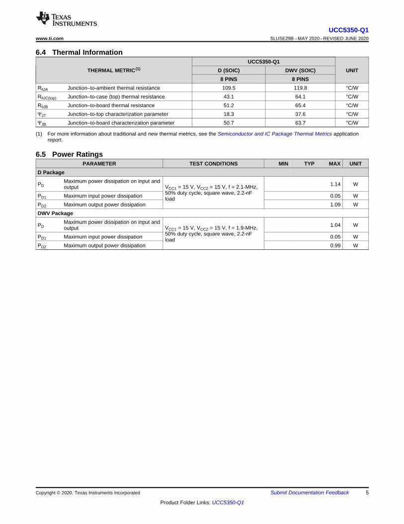
6.4 Thermal Information
THERMAL METRIC (1)UCC5350-Q1
UNITD (SOIC) DWV (SOIC)8 PINS 8 PINS
RθJA Junction–to-ambient thermal resistance 109.5 119.8 °C/WRθJC(top) Junction–to-case (top) thermal resistance 43.1 64.1 °C/WRθJB Junction–to-board thermal resistance 51.2 65.4 °C/WΨJT Junction–to-top characterization parameter 18.3 37.6 °C/WΨJB Junction–to-board characterization parameter 50.7 63.7 °C/W
6.5 Power RatingsPARAMETER TEST CONDITIONS MIN TYP MAX UNIT
D Package
PDMaximum power dissipation on input andoutput VCC1 = 15 V, VCC2 = 15 V, f = 2.1-MHz,
50% duty cycle, square wave, 2.2-nFload
1.14 W
PD1 Maximum input power dissipation 0.05 WPD2 Maximum output power dissipation 1.09 WDWV Package
PDMaximum power dissipation on input andoutput VCC1 = 15 V, VCC2 = 15 V, f = 1.9-MHz,
50% duty cycle, square wave, 2.2-nFload
1.04 W
PD1 Maximum input power dissipation 0.05 WPD2 Maximum output power dissipation 0.99 W
6
UCC5350-Q1SLUSE29B –MAY 2020–REVISED JUNE 2020 www.ti.com
Product Folder Links: UCC5350-Q1
Submit Documentation Feedback Copyright © 2020, Texas Instruments Incorporated
(1) Creepage and clearance requirements should be applied according to the specific equipment isolation standards of an application. Careshould be taken to maintain the creepage and clearance distance of a board design to ensure that the mounting pads of the isolator onthe printed-circuit board do not reduce this distance. Creepage and clearance on a printed-circuit board become equal in certain cases.Techniques such as inserting grooves, ribs, or both on a printed circuit board are used to help increase these specifications.
(2) This coupler is suitable for basic electrical insulation only within the maximum operating ratings. Compliance with the safety ratings shallbe ensured by means of suitable protective circuits.
(3) Testing is carried out in air or oil to determine the intrinsic surge immunity of the isolation barrier.(4) Apparent charge is electrical discharge caused by a partial discharge (pd).(5) All pins on each side of the barrier tied together creating a two-pin device.
6.6 Insulation Specifications for D Package
PARAMETER TEST CONDITIONSVALUE
UNITD
CLR External Clearance (1) Shortest pin–to-pin distance through air ≥ 4 mm
CPG External Creepage (1) Shortest pin–to-pin distance across the packagesurface ≥ 4 mm
DTI Distance through the insulation Minimum internal gap (internal clearance) > 21 µmCTI Comparative tracking index DIN EN 60112 (VDE 0303–11); IEC 60112 > 600 V
Material Group According to IEC 60664–1 I
Overvoltage category per IEC 60664-1Rated mains voltage ≤ 150 VRMS I-IVRated mains voltage ≤ 300 VRMS I-III
DIN V VDE 0884–11: 2017–01 (2)
VIORMMaximum repetitive peakisolation voltage AC voltage (bipolar) 990 VPK
VIOWMMaximum isolation workingvoltage
AC voltage (sine wave); time dependent dielectricbreakdown (TDDB) test 700 VRMS
VIOTMMaximum transient isolationvoltage
VTEST = VIOTM, t = 60 s (qualification);VTEST = 1.2 × VIOTM, t = 1 s (100% production) 4242 VPK
VIOSMMaximum surge isolationvoltage (3)
Test method per IEC 62368-1, 1.2/50-µs waveform,VTEST = 1.3 × VIOSM (qualification) 4242 VPK
qpd Apparent charge (4)
Method a: After I/O safety test subgroup 2/3,Vini = VIOTM, tini = 60 sVpd(m) = 1.2 × VIORM, tm = 10 s
≤ 5
pC
Method a: After environmental tests subgroup 1,Vini = VIOTM, tini = 60 s;Vpd(m) = 1.2 × VIORM, tm = 10 s
≤ 5
Method b1: At routine test (100% production) andpreconditioning (type test),Vini = 1.2 x VIOTM, tini = 1 s;Vpd(m) = 1.5 × VIORM, tm = 1 s
≤ 5
CIOBarrier capacitance, input tooutput (5) VIO = 0.4 × sin (2πft), f = 1 MHz 1.2 pF
RIOIsolation resistance, input tooutput (5)
VIO = 500 V, TA = 25°C > 1012
ΩVIO = 500 V, 100°C ≤ TA ≤ 125°C > 1011
VIO = 500 V at TS = 150°C > 109
Pollution degree 2Climatic category 40/125/21
UL 1577
VISO Withstand isolation voltage VTEST = VISO, t = 60 s (qualification); VTEST = 1.2 ×VISO, t = 1 s (100% production) 3000 VRMS
7
UCC5350-Q1www.ti.com SLUSE29B –MAY 2020–REVISED JUNE 2020
Product Folder Links: UCC5350-Q1
Submit Documentation FeedbackCopyright © 2020, Texas Instruments Incorporated
(1) Creepage and clearance requirements should be applied according to the specific equipment isolation standards of an application. Careshould be taken to maintain the creepage and clearance distance of a board design to ensure that the mounting pads of the isolator onthe printed-circuit board do not reduce this distance. Creepage and clearance on a printed-circuit board become equal in certain cases.Techniques such as inserting grooves, ribs, or both on a printed circuit board are used to help increase these specifications.
(2) This coupler is suitable for safe electrical insulation only within the safety ratings. Compliance with the safety ratings shall be ensured bymeans of suitable protective circuits.
(3) Testing is carried out in air or oil to determine the intrinsic surge immunity of the isolation barrier.(4) Apparent charge is electrical discharge caused by a partial discharge (pd).(5) All pins on each side of the barrier tied together creating a two-pin device.
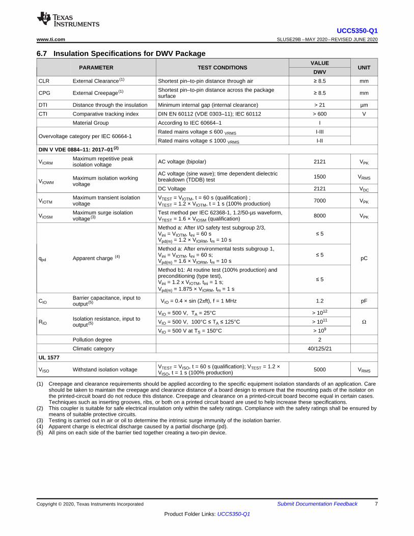
6.7 Insulation Specifications for DWV Package
PARAMETER TEST CONDITIONSVALUE
UNITDWV
CLR External Clearance (1) Shortest pin–to-pin distance through air ≥ 8.5 mm
CPG External Creepage (1) Shortest pin–to-pin distance across the packagesurface ≥ 8.5 mm
DTI Distance through the insulation Minimum internal gap (internal clearance) > 21 µmCTI Comparative tracking index DIN EN 60112 (VDE 0303–11); IEC 60112 > 600 V
Material Group According to IEC 60664–1 I
Overvoltage category per IEC 60664-1Rated mains voltage ≤ 600 VRMS I-IIIRated mains voltage ≤ 1000 VRMS I-II
DIN V VDE 0884–11: 2017–01 (2)
VIORMMaximum repetitive peakisolation voltage AC voltage (bipolar) 2121 VPK
VIOWMMaximum isolation workingvoltage
AC voltage (sine wave); time dependent dielectricbreakdown (TDDB) test 1500 VRMS
DC Voltage 2121 VDC
VIOTMMaximum transient isolationvoltage
VTEST = VIOTM, t = 60 s (qualification) ;VTEST = 1.2 × VIOTM, t = 1 s (100% production) 7000 VPK
VIOSMMaximum surge isolationvoltage (3)
Test method per IEC 62368-1, 1.2/50-µs waveform,VTEST = 1.6 × VIOSM (qualification) 8000 VPK
qpd Apparent charge (4)
Method a: After I/O safety test subgroup 2/3,Vini = VIOTM, tini = 60 sVpd(m) = 1.2 × VIORM, tm = 10 s
≤ 5
pC
Method a: After environmental tests subgroup 1,Vini = VIOTM, tini = 60 s;Vpd(m) = 1.6 × VIORM, tm = 10 s
≤ 5
Method b1: At routine test (100% production) andpreconditioning (type test),Vini = 1.2 x VIOTM, tini = 1 s;Vpd(m) = 1.875 × VIORM, tm = 1 s
≤ 5
CIOBarrier capacitance, input tooutput (5) VIO = 0.4 × sin (2πft), f = 1 MHz 1.2 pF
RIOIsolation resistance, input tooutput (5)
VIO = 500 V, TA = 25°C > 1012
ΩVIO = 500 V, 100°C ≤ TA ≤ 125°C > 1011
VIO = 500 V at TS = 150°C > 109
Pollution degree 2Climatic category 40/125/21
UL 1577
VISO Withstand isolation voltage VTEST = VISO, t = 60 s (qualification); VTEST = 1.2 ×VISO, t = 1 s (100% production) 5000 VRMS
8
UCC5350-Q1SLUSE29B –MAY 2020–REVISED JUNE 2020 www.ti.com
Product Folder Links: UCC5350-Q1
Submit Documentation Feedback Copyright © 2020, Texas Instruments Incorporated
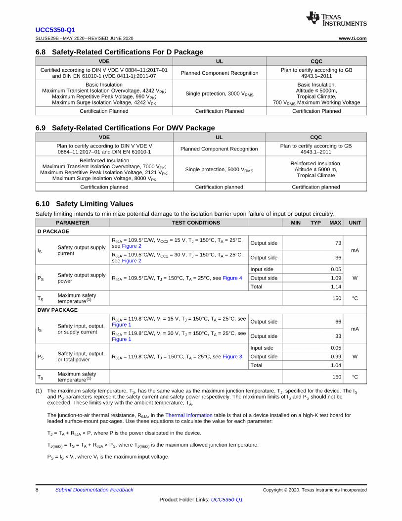
6.8 Safety-Related Certifications For D PackageVDE UL CQC
Certified according to DIN V VDE V 0884–11:2017–01and DIN EN 61010-1 (VDE 0411-1):2011-07 Planned Component Recognition Plan to certify according to GB
4943.1–2011Basic Insulation
Maximum Transient Isolation Overvoltage, 4242 VPK;Maximum Repetitive Peak Voltage, 990 VPK;Maximum Surge Isolation Voltage, 4242 VPK
Single protection, 3000 VRMS
Basic Insulation,Altitude ≤ 5000m,Tropical Climate,
700 VRMS Maximum Working VoltageCertification Planned Certification Planned Certification Planned
6.9 Safety-Related Certifications For DWV PackageVDE UL CQC
Plan to certify according to DIN V VDE V0884–11:2017–01 and DIN EN 61010-1 Planned Component Recognition Plan to certify according to GB
4943.1–2011Reinforced Insulation
Maximum Transient Isolation Overvoltage, 7000 VPK;Maximum Repetitive Peak Isolation Voltage, 2121 VPK;
Maximum Surge Isolation Voltage, 8000 VPK
Single protection, 5000 VRMS
Reinforced Insulation,Altitude ≤ 5000 m,Tropical Climate
Certification planned Certification planned Certification planned
(1) The maximum safety temperature, TS, has the same value as the maximum junction temperature, TJ, specified for the device. The ISand PS parameters represent the safety current and safety power respectively. The maximum limits of IS and PS should not beexceeded. These limits vary with the ambient temperature, TA.
The junction-to-air thermal resistance, RθJA, in the Thermal Information table is that of a device installed on a high-K test board forleaded surface-mount packages. Use these equations to calculate the value for each parameter:
TJ = TA + RθJA × P, where P is the power dissipated in the device.
TJ(max) = TS = TA + RθJA × PS, where TJ(max) is the maximum allowed junction temperature.
PS = IS × VI, where VI is the maximum input voltage.
6.10 Safety Limiting ValuesSafety limiting intends to minimize potential damage to the isolation barrier upon failure of input or output circuitry.
PARAMETER TEST CONDITIONS MIN TYP MAX UNITD PACKAGE
ISSafety output supplycurrent
RθJA = 109.5°C/W, VCC2 = 15 V, TJ = 150°C, TA = 25°C,see Figure 2 Output side 73
mARθJA = 109.5°C/W, VCC2 = 30 V, TJ = 150°C, TA = 25°C,see Figure 2 Output side 36
PSSafety output supplypower RθJA = 109.5°C/W, TJ = 150°C, TA = 25°C, see Figure 4
Input side 0.05WOutput side 1.09
Total 1.14
TSMaximum safetytemperature (1) 150 °C
DWV PACKAGE
ISSafety input, output,or supply current
RθJA = 119.8°C/W, VI = 15 V, TJ = 150°C, TA = 25°C, seeFigure 1 Output side 66
mARθJA = 119.8°C/W, VI = 30 V, TJ = 150°C, TA = 25°C, seeFigure 1 Output side 33
PSSafety input, output,or total power RθJA = 119.8°C/W, TJ = 150°C, TA = 25°C, see Figure 3
Input side 0.05WOutput side 0.99
Total 1.04
TSMaximum safetytemperature (1) 150 °C

9
UCC5350-Q1www.ti.com SLUSE29B –MAY 2020–REVISED JUNE 2020
Product Folder Links: UCC5350-Q1
Submit Documentation FeedbackCopyright © 2020, Texas Instruments Incorporated
6.11 Electrical CharacteristicsVCC1 = 3.3 V or 5 V, 0.1-µF capacitor from VCC1 to GND1, VCC2= 15 V, 1-µF capacitor from VCC2 to VEE2, CL = 100-pF, TJ =–40°C to +125°C, (unless otherwise noted)
PARAMETER TEST CONDITIONS MIN TYP MAX UNITSUPPLY CURRENTSIVCC1 Input supply quiescent current 1.67 2.4 mA
IVCC2Output supply quiescentcurrent 1.1 1.8 mA
SUPPLY VOLTAGE UNDERVOLTAGE THRESHOLDS
VIT+(UVLO1)VCC1 Positive-going UVLOthreshold voltage 2.6 2.8 V
VIT– (UVLO1)VCC1 Negative-going UVLOthreshold voltage 2.4 2.5 V
Vhys(UVLO1)VCC1 UVLO thresholdhysteresis 0.1 V
OUTPUT SUPPLY VOLTAGE UNDERVOLTAGE THRESHOLDS
VIT+(UVLO2)VCC2 Positive-going UVLOthreshold voltage 12 13 V
VIT–(UVLO2)VCC2 Negative-going UVLOthreshold voltage 10.3 11 V
Vhys(UVLO2)VCC2 UVLO threshold voltagehysteresis 1 V
LOGIC I/O
VIT+(IN)Positive-going input thresholdvoltage (IN+, IN–) 0.55 × VCC1
0.7 ×VCC1
V
VIT–(IN)Negative-going input thresholdvoltage (IN+, IN–) 0.3 × VCC1 0.45 × VCC1 V
Vhys(IN)Input hysteresis voltage (IN+,IN–) 0.1 × VCC1 V
IIH High-level input leakage at IN+ IN+ = VCC1 40 240 µA
IIL Low-level input leakage at IN–IN– = GND1 –240 –40
µAIN– = GND1 – 5 V –310 –80
GATE DRIVER STAGE
VOHHigh-level output voltage(OUT) IOUT = –20 mA 100 240 mV
VOLLow level output voltage(OUT) IN+ = low, IN– = high; IO = 20 mA 5 7 mV
IOH Peak source current IN+ = high, IN– = low 5 10 AIOL Peak sink current IN+ = low, IN– = high 5 10 AActive Miller ClampVCLAMP Low-level clamp voltage ICLAMP = 20mA 7 10 mVICLAMP Clamp low-level current VCLAMP = VEE2 + 15 V 5 10 A
ICLAMP(L)Clamp low-level current forlow output voltage VCLAMP = VEE2 + 2 V 5 10 A
VCLAMP-TH Clamp threshold voltage 2.1 2.3 VSHORT CIRCUIT CLAMPING
VCLP-OUTClamping voltage(VOUT –VCC2)
IN+ = high, IN– = low, tCLAMP = 10 µs,IOUT= 500 mA 1 1.3 V
VCLP-OUTClamping voltage( VEE2 – VOUT)
IN+ = low, IN– = high, tCLAMP = 10 µs,IOUT = –500 mA 1.5
VIN+ = low, IN– = high,IOUT = –20 mA 0.9 1
ACTIVE PULLDOWN
VOUTSDActive pulldown voltage onOUT IOUT = 0.1 × IOUT(typ), VCC2 = open 1.8 2.5 V
Ambient Temperature (qC)
Safe
ty L
imitin
g P
ow
er
(mW
)
0 50 100 150 2000
300
600
900
1200
1500
Ambient Temperature (qC)
Safe
ty L
imitin
g P
ow
er
(mW
)
0 50 100 150 2000
300
600
900
1200
1500
D001Ther
Ambient Temperature (qC)
Safe
ty L
imitin
g C
urr
ent (m
A)
0 50 100 150 2000
20
40
60
80VCC2=15VVCC2=30V
Ambient Temperature (qC)
Safe
ty L
imitin
g C
urr
ent
(mA
)
0 50 100 150 2000
20
40
60
80
D001Ther
VCC2=15VVCC2=30V
10
UCC5350-Q1SLUSE29B –MAY 2020–REVISED JUNE 2020 www.ti.com
Product Folder Links: UCC5350-Q1
Submit Documentation Feedback Copyright © 2020, Texas Instruments Incorporated
6.12 Switching CharacteristicsVCC1 = 3.3 V or 5 V, 0.1-µF capacitor from VCC1 to GND1, VCC2= 15 V, 1-µF capacitor from VCC2 to VEE2, TJ = –40°C to+125°C, (unless otherwise noted)
PARAMETER TEST CONDITIONS MIN TYP MAX UNITtr Output-signal rise time CLOAD = 1 nF 10 26 nstf Output-signal fall time CLOAD = 1 nF 10 22 nstPLH Propagation delay, high CLOAD = 100 pF 65 100 nstPHL Propagation delay, low CLOAD = 100 pF 65 100 nstUVLO1_rec UVLO recovery delay of VCC1 See Figure 29 30 µstUVLO2_rec UVLO recovery delay of VCC2 See Figure 29 50 µs
tPWDPulse width distortion|tPHL – tPLH| CLOAD = 100 pF 1 20 ns
tsk(pp) Part-to-part skew CLOAD = 100 pF 1 25 ns
CMTI Common-mode transientimmunity PWM is tied to GND or VCC1, VCM = 1200 V 100 120 kV/µs
6.13 Insulation Characteristics Curves
Figure 1. Thermal Derating Curve for Limiting Current perVDE for DWV Package
Figure 2. Thermal Derating Curve for Limiting Current perVDE for D Package
Figure 3. Thermal Derating Curve for Limiting Power perVDE for DWV Package
Figure 4. Thermal Derating Curve for Limiting Power perVDE for D Package

Frequency (MHz)
ICC
1 S
upply
Curr
ent (m
A)
0.1 0.2 0.3 0.4 0.5 0.6 0.7 0.8 0.9 1 1.11.6
1.62
1.64
1.66
1.68
1.7
1.72
1.74
1.76
1.78
1.8
ICC1Temperature (qC)
ICC
2 S
upply
Curr
ent (m
A)
-60 -40 -20 0 20 40 60 80 100 120 1400.6
0.75
0.9
1.05
1.2
1.35
1.5
1.65
1.8
1.95
2.1
ICC2
Temperature (qC)
ICC
1 S
upply
Curr
ent (m
A)
-60 -40 -20 0 20 40 60 80 100 120 1401
1.05
1.1
1.15
1.2
1.25
1.3
1.35
1.4
1.45
1.5
ICC1Temperature (qC)
ICC
1 S
upply
Curr
ent (m
A)
-60 -40 -20 0 20 40 60 80 100 120 1402
2.05
2.1
2.15
2.2
2.25
2.3
2.35
2.4
2.45
2.5
UCC5
VCC2 (V)
Pea
k O
utp
ut C
urr
ent
Hig
h I
OH (
A)
14 16 18 20 22 24 26 28 30 32 348
9
10
11
12
13
14
15
16
IOH_VCC2 (V)
Peak O
utp
ut C
urr
ent Low
IO
L (
A)
14 16 18 20 22 24 26 28 30 32 348
9
10
11
12
13
14
15
16
IOL_
11
UCC5350-Q1www.ti.com SLUSE29B –MAY 2020–REVISED JUNE 2020
Product Folder Links: UCC5350-Q1
Submit Documentation FeedbackCopyright © 2020, Texas Instruments Incorporated
6.14 Typical CharacteristicsVCC1 = 3.3 V or 5 V, 0.1-µF capacitor from VCC1 to GND1, VCC2= 15 V, 1-µF capacitor from VCC2 to VEE2, CLOAD = 1 nF, TJ =–40°C to +125°C, (unless otherwise noted)
CLOAD = 150 nF
Figure 5. Output-High Drive Current vs Output Voltage
CLOAD = 150 nF
Figure 6. Output-Low Drive Current vs Output Voltage
IN+ = L IN– = H
Figure 7. ICC1 Supply Current vs Temperature
IN+ = H IN– = L
Figure 8. ICC1 Supply Current vs Temperature
Duty Cycle = 50% T = 25°C
Figure 9. ICC1 Supply Current vs Input Frequency
IN+ = L IN– = H
Figure 10. ICC2 Supply Current vs Temperature

Temperature (qC)
Fa
ll T
ime
tf (n
s)
-60 -40 -20 0 20 40 60 80 100 120 1406.75
7
7.25
7.5
7.75
8
8.25
8.5
8.75
9
9.25
tf_vTemperature (qC)
Pro
pa
ga
tio
n D
ela
y t
PL
H (
ns)
-60 -40 -20 0 20 40 60 80 100 120 14050
50.5
51
51.5
52
52.5
53
53.5
54
54.5
55
tPLH
Temperature (qC)
Ris
e T
ime t
r (n
s)
-60 -40 -20 0 20 40 60 80 100 120 1406
6.4
6.8
7.2
7.6
8
8.4
8.8
9.2
9.6
10
tr_vLoad Capacitance (nF)
ICC
2 S
upply
Curr
ent (m
A)
1 2 3 4 5 6 7 8 9 10 111.08
1.12
1.16
1.2
1.24
1.28
1.32
1.36
1.4
1.44
1.48
ICC2
Temperature (qC)
ICC
2 S
upply
Curr
ent (m
A)
-60 -40 -20 0 20 40 60 80 100 120 1401
1.1
1.2
1.3
1.4
1.5
1.6
1.7
1.8
1.9
2
UCC5Frequency (MHz)
ICC
2 S
upply
Curr
ent (m
A)
0.1 0.2 0.3 0.4 0.5 0.6 0.7 0.8 0.9 1 1.11.6
1.61
1.62
1.63
1.64
1.65
1.66
1.67
1.68
1.69
1.7
ICC2
12
UCC5350-Q1SLUSE29B –MAY 2020–REVISED JUNE 2020 www.ti.com
Product Folder Links: UCC5350-Q1
Submit Documentation Feedback Copyright © 2020, Texas Instruments Incorporated
Typical Characteristics (continued)VCC1 = 3.3 V or 5 V, 0.1-µF capacitor from VCC1 to GND1, VCC2= 15 V, 1-µF capacitor from VCC2 to VEE2, CLOAD = 1 nF, TJ =–40°C to +125°C, (unless otherwise noted)
IN+ = H IN– = L
Figure 11. ICC2 Supply Current vs Temperature
Duty Cycle = 50% T = 25°C
Figure 12. ICC2 Supply Current vs Input Frequency
fSW = 1 kHz
Figure 13. ICC2 Supply Current vs Load Capacitance Figure 14. Rise Time vs Temperature
Figure 15. Fall Time vs Temperature Figure 16. Propagation Delay tPLH vs Temperature

Temperature (qC)
VC
LA
MP
-TH (
V)
-60 -40 -20 0 20 40 60 80 100 120 1400.5
0.75
1
1.25
1.5
1.75
2
2.25
2.5
2.75
3
VCLM
Temperature (qC)
VC
LA
MP (
mV
)
-75 -45 -15 15 45 75 105 135 165-10
-7.5
-5
-2.5
0
2.5
5
7.5
10
12.5
15
17.5
20
22.5
25
D022
0mA5mA10mA15mA20mA
Load Capacitance (nF)
Fall
Tim
e t
f (n
s)
0 1 2 3 4 5 6 7 8 9 100
4
8
12
16
20
24
28
32
36
40
tf_v
Load Capacitance (nF)
Ris
e T
ime t
r (n
s)
0 1 2 3 4 5 6 7 8 9 100
3
6
9
12
15
18
21
24
27
30
tr_vTemperature (qC)
Pro
pagation D
ela
y tP
HL (
ns)
-60 -40 -20 0 20 40 60 80 100 120 14050
51
52
53
54
55
56
57
58
59
60
tPHL
13
UCC5350-Q1www.ti.com SLUSE29B –MAY 2020–REVISED JUNE 2020
Product Folder Links: UCC5350-Q1
Submit Documentation FeedbackCopyright © 2020, Texas Instruments Incorporated
Typical Characteristics (continued)VCC1 = 3.3 V or 5 V, 0.1-µF capacitor from VCC1 to GND1, VCC2= 15 V, 1-µF capacitor from VCC2 to VEE2, CLOAD = 1 nF, TJ =–40°C to +125°C, (unless otherwise noted)
Figure 17. Propagation Delay tPHL vs Temperature
fSW = 1 kHz RGH = 0 Ω RGL = 0 Ω
Figure 18. Rise Time vs Load Capacitance
fSW = 1 kHz RGH = 0 Ω RGL = 0 Ω
Figure 19. Fall Time vs Load CapacitanceFigure 20. VCLAMP vs Temperature
Figure 21. VCLAMP-TH vs Temperature

tPLH tPHL
trtf
50%
10%
90%
50%
OUT
IN+
IN±
tPLH tPHL
tr
tf
50%
10%
90%
50%
OUT
IN+
IN± 0 V
14
UCC5350-Q1SLUSE29B –MAY 2020–REVISED JUNE 2020 www.ti.com
Product Folder Links: UCC5350-Q1
Submit Documentation Feedback Copyright © 2020, Texas Instruments Incorporated
7 Parameter Measurement Information
7.1 Propagation Delay, Inverting, and Noninverting ConfigurationFigure 22 shows the propagation delay for noninverting configurations. Figure 23 shows the propagation delaywith the inverting configuration. These figures also demonstrate the method used to measure the rise (tr) and fall(tf) times.
Figure 22. Propagation Delay, Noninverting Configuration
Figure 23. Propagation Delay, Inverting Configuration
VCC1
IN+
IN±
GND1
VEE2
OUT
VCC2
C3 C4
15 V
PWM
C2C1
VCM
± +
CLAMP
Copyright © 2017, Texas Instruments Incorporated
5 V
ISO
LA
TIO
N B
AR
RIE
R
15
UCC5350-Q1www.ti.com SLUSE29B –MAY 2020–REVISED JUNE 2020
Product Folder Links: UCC5350-Q1
Submit Documentation FeedbackCopyright © 2020, Texas Instruments Incorporated
Propagation Delay, Inverting, and Noninverting Configuration (continued)7.1.1 CMTI TestingFigure 24 is a simplified diagram of the CMTI testing configuration.
Figure 24. CMTI Test Circuit
TX IN
RX OUT
Carrier signal through isolation barrier
TX IN
Oscillator
OOK
Modulation
Transmitter
Emissions
Reduction
Techniques
TX Signal
Conditioning
Envelope
Detection
RX Signal
Conditioning
Receiver
RX OUTSiO2 based
Capacitive
Isolation
Barrier
16
UCC5350-Q1SLUSE29B –MAY 2020–REVISED JUNE 2020 www.ti.com
Product Folder Links: UCC5350-Q1
Submit Documentation Feedback Copyright © 2020, Texas Instruments Incorporated
8 Detailed Description
8.1 OverviewThe isolation inside the UCC5350-Q1 is implemented with high-voltage SiO2-based capacitors. The signal acrossthe isolation has an on-off keying (OOK) modulation scheme to transmit the digital data across a silicon dioxidebased isolation barrier (see Figure 26). The transmitter sends a high-frequency carrier across the barrier torepresent one digital state and sends no signal to represent the other digital state. The receiver demodulates thesignal after advanced signal conditioning and produces the output through a buffer stage. The UCC5350-Q1 alsoincorporates advanced circuit techniques to maximize the CMTI performance and minimize the radiatedemissions from the high frequency carrier and IO buffer switching. The conceptual block diagram of a digitalcapacitive isolator, Figure 25, shows a functional block diagram of a typical channel. Figure 26 shows aconceptual detail of how the OOK scheme works.
Figure 25 shows how the input signal passes through the capacitive isolation barrier through modulation (OOK)and signal conditioning.
8.2 Functional Block Diagram
Figure 25. Conceptual Block Diagram of a Capacitive Data Channel
Figure 26. On-Off Keying (OOK) Based Modulation Scheme
VEE2
VCC2
Level
Shifting
and
Control
Logic
UVLO2UVLO1
GND1
VCC1
IN±
IN+
OUT
CLAMP
2 V
ISO
LA
TIO
NB
AR
RIE
R
VCC2
17
UCC5350-Q1www.ti.com SLUSE29B –MAY 2020–REVISED JUNE 2020
Product Folder Links: UCC5350-Q1
Submit Documentation FeedbackCopyright © 2020, Texas Instruments Incorporated
Functional Block Diagram (continued)
Figure 27. Functional Block Diagram
8.3 Feature Description
8.3.1 Power SupplyThe VCC1 input power supply supports a wide voltage range from 3 V to 15 V and the VCC2 output supplysupports a voltage range from 13.2 V to 33 V.
For operation with unipolar supply, the VCC2 supply is connected to 15 V with respect to VEE2 for IGBTs, and 20V for SiC MOSFETs. The VEE2 supply is connected to 0 V. In this use case, the Miller clamp helps to prevent afalse turn-on of the power switch without a negative voltage rail. The Miller clamping function is implemented byadding a low impedance path between the gate of the power device and the VEE2 supply. Miller current sinksthrough the clamp pin, which clamps the gate voltage to be lower than the turn-on threshold value for the gate.
8.3.2 Input StageThe input pins (IN+ and IN–) of the UCC5350-Q1 are based on CMOS-compatible input-threshold logic that iscompletely isolated from the VCC2 supply voltage. The input pins are easy to drive with logic-level control signals(such as those from 3.3-V microcontrollers), because the UCC5350-Q1 has a typical high threshold (VIT+(IN)) of0.55 × VCC1 and a typical low threshold of 0.45 × VCC1. A wide hysteresis (Vhys(IN)) of 0.1 × VCC1 makes for goodnoise immunity and stable operation. If either of the inputs are left open, 128 kΩ of internal pull-down resistanceforces the IN+ pin low and 128 kΩ of internal resistance pulls IN– high. However, TI still recommends groundingan input or tying to VCC1 if it is not being used for improved noise immunity.
Because the input side of the UCC5350-Q1 is isolated from the output driver, the input signal amplitude can belarger or smaller than VCC2 provided that it does not exceed the recommended limit. This feature allows greaterflexibility when integrating the gate-driver with control signal sources and allows the user to choose the mostefficient VCC2 for any gate. However, the amplitude of any signal applied to IN+ or IN– must never be at a voltagehigher than VCC1.
Level Shifting
and
Control
LogicROL
ROH
RNMOS
UVLO2 VCC2
CLAMP
OUT
VEE2
2 V
18
UCC5350-Q1SLUSE29B –MAY 2020–REVISED JUNE 2020 www.ti.com
Product Folder Links: UCC5350-Q1
Submit Documentation Feedback Copyright © 2020, Texas Instruments Incorporated
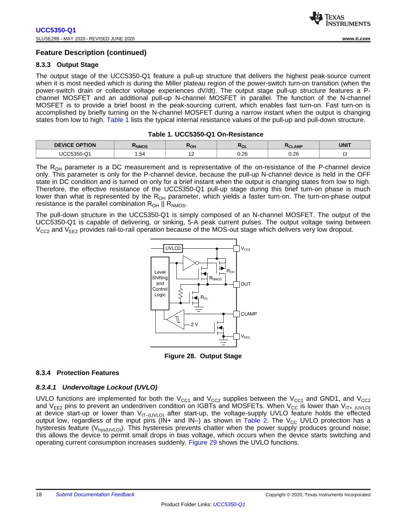
Feature Description (continued)8.3.3 Output StageThe output stage of the UCC5350-Q1 feature a pull-up structure that delivers the highest peak-source currentwhen it is most needed which is during the Miller plateau region of the power-switch turn-on transition (when thepower-switch drain or collector voltage experiences dV/dt). The output stage pull-up structure features a P-channel MOSFET and an additional pull-up N-channel MOSFET in parallel. The function of the N-channelMOSFET is to provide a brief boost in the peak-sourcing current, which enables fast turn-on. Fast turn-on isaccomplished by briefly turning on the N-channel MOSFET during a narrow instant when the output is changingstates from low to high. Table 1 lists the typical internal resistance values of the pull-up and pull-down structure.
Table 1. UCC5350-Q1 On-ResistanceDEVICE OPTION RNMOS ROH ROL RCLAMP UNIT
UCC5350-Q1 1.54 12 0.26 0.26 Ω
The ROH parameter is a DC measurement and is representative of the on-resistance of the P-channel deviceonly. This parameter is only for the P-channel device, because the pull-up N-channel device is held in the OFFstate in DC condition and is turned on only for a brief instant when the output is changing states from low to high.Therefore, the effective resistance of the UCC5350-Q1 pull-up stage during this brief turn-on phase is muchlower than what is represented by the ROH parameter, which yields a faster turn-on. The turn-on-phase outputresistance is the parallel combination ROH || RNMOS.
The pull-down structure in the UCC5350-Q1 is simply composed of an N-channel MOSFET. The output of theUCC5350-Q1 is capable of delivering, or sinking, 5-A peak current pulses. The output voltage swing betweenVCC2 and VEE2 provides rail-to-rail operation because of the MOS-out stage which delivers very low dropout.
Figure 28. Output Stage
8.3.4 Protection Features
8.3.4.1 Undervoltage Lockout (UVLO)UVLO functions are implemented for both the VCC1 and VCC2 supplies between the VCC1 and GND1, and VCC2and VEE2 pins to prevent an underdriven condition on IGBTs and MOSFETs. When VCC is lower than VIT+ (UVLO)at device start-up or lower than VIT–(UVLO) after start-up, the voltage-supply UVLO feature holds the effectedoutput low, regardless of the input pins (IN+ and IN–) as shown in Table 2. The VCC UVLO protection has ahysteresis feature (Vhys(UVLO)). This hysteresis prevents chatter when the power supply produces ground noise;this allows the device to permit small drops in bias voltage, which occurs when the device starts switching andoperating current consumption increases suddenly. Figure 29 shows the UVLO functions.

IN+
VCC1
VCC2
VOUT
VIT+ (UVLO2)
VIT± (UVLO2)
IN+
VCC1
VCC2
VOUT
VIT+ (UVLO1)
VIT±(UVLO1)
tUVLO1_rec
tUVLO2_rec
19
UCC5350-Q1www.ti.com SLUSE29B –MAY 2020–REVISED JUNE 2020
Product Folder Links: UCC5350-Q1
Submit Documentation FeedbackCopyright © 2020, Texas Instruments Incorporated
Table 2. UCC5350-Q1 VCC1 UVLO Logic
CONDITIONINPUTS OUTPUT
IN+ IN– OUT
VCC1 – GND1 < VIT+(UVLO1) during device start-up
H L LL H LH H LL L L
VCC1 – GND1 < VIT–(UVLO1) after device start-up
H L LL H LH H LL L L
Table 3. UCC5350-Q1 VCC2 UVLO Logic
CONDITIONINPUTS OUTPUT
IN+ IN– OUT
VCC2 – VEE2 < VIT+(UVLO2) during device start-up
H L LL H LH H LL L L
VCC2 – VEE2 < VIT–(UVLO2) after device start-up
H L LL H LH H LL L L
When VCC1 or VCC2 drops below the UVLO1 or UVLO2 threshold, a delay, tUVLO1_rec or tUVLO2_rec, occurs on theoutput when the supply voltage rises above VIT+(UVLO) or VIT+(UVLO2) again. Figure 29 shows this delay.
Figure 29. UVLO Functions
20
UCC5350-Q1SLUSE29B –MAY 2020–REVISED JUNE 2020 www.ti.com
Product Folder Links: UCC5350-Q1
Submit Documentation Feedback Copyright © 2020, Texas Instruments Incorporated
8.3.4.2 Active PulldownThe active pull-down function is used to pull the IGBT or MOSFET gate to the low state when no power isconnected to the VCC2 supply. This feature prevents false IGBT and MOSFET turn-on on the OUT and CLAMPpins by clamping the output to approximately 2 V.
When the output stages of the driver are in an unbiased or UVLO condition, the driver outputs are held low by anactive clamp circuit that limits the voltage rise on the driver outputs. In this condition, the upper PMOS isresistively held off by a pull-up resistor while the lower NMOS gate is tied to the driver output through a 500-kΩresistor. In this configuration, the output is effectively clamped to the threshold voltage of the lower NMOSdevice, which is approximately 1.5 V when no bias power is available.
8.3.4.3 Short-Circuit ClampingThe short-circuit clamping function is used to clamp voltages at the driver output and pull the active Miller clamppins slightly higher than the VCC2 voltage during short-circuit conditions. The short-circuit clamping function helpsprotect the IGBT or MOSFET gate from overvoltage breakdown or degradation. The short-circuit clampingfunction is implemented by adding a diode connection between the dedicated pins and the VCC2 pin inside thedriver. The internal diodes can conduct up to 500-mA current for a duration of 10 µs and a continuous current of20 mA. Use external Schottky diodes to improve current conduction capability as needed.
8.3.4.4 Active Miller ClampThe active Miller-clamp function is used to prevent false turn-on of the power switches caused by Miller current inapplications where a unipolar power supply is used. The active Miller-clamp function is implemented by adding alow impedance path between the power-switch gate terminal and ground (VEE2) to sink the Miller current. Withthe Miller-clamp function, the power-switch gate voltage is clamped to less than 2 V during the off state.Figure 31 shows a typical application circuit of this function.
8.4 Device Functional ModesTable 4 lists the functional modes for the UCC5350-Q1 assuming VCC1 and VCC2 are in the recommended range.
Table 4. Function TableIN+ IN– OUTLow X Low
X High LowHigh Low High

1
2
3
4
5
8
6
VCC1
IN+
IN±
GND1 VEE2
OUT
VCC2
20 V
5.5 V
40 V
7 CLAMP
21
UCC5350-Q1www.ti.com SLUSE29B –MAY 2020–REVISED JUNE 2020
Product Folder Links: UCC5350-Q1
Submit Documentation FeedbackCopyright © 2020, Texas Instruments Incorporated
8.4.1 ESD StructureFigure 30 shows the multiple diodes involved in the ESD protection components of the UCC5350-Q1. Thisprovides pictorial representation of the absolute maximum rating for the device.
Figure 30. ESD Structure

VCC1
IN+
IN±
GND1
VEE2
VCC2
OUT
CLAMP
C3 C4
15 V
5 V
C2C1
Copyright © 2017, Texas Instruments Incorporated
Signal Emitter
Power Emitter
RG
PWMRin
Cin
22
UCC5350-Q1SLUSE29B –MAY 2020–REVISED JUNE 2020 www.ti.com
Product Folder Links: UCC5350-Q1
Submit Documentation Feedback Copyright © 2020, Texas Instruments Incorporated
9 Application and Implementation
NOTEInformation in the following applications sections is not part of the TI componentspecification, and TI does not warrant its accuracy or completeness. TI’s customers areresponsible for determining suitability of components for their purposes. Customers shouldvalidate and test their design implementation to confirm system functionality.
9.1 Application InformationThe UCC5350-Q1 is a simple, isolated gate driver for power semiconductor devices, such as MOSFETs, IGBTs,or SiC MOSFETs. The family of devices is intended for use in applications such as motor control, solar inverters,switched-mode power supplies, and industrial inverters.
The UCC5350-Q1 has active Miller clamping, which can be used to prevent false turn-on of the power transistorsinduced by the Miller current. The device comes in an 8-pin D and 8-pin DWV package and has creepage, orclearance, of 4 mm and 8.5 mm, respectively, which is suitable for applications where basic or reinforcedisolation is required. The UCC5350-Q1 offers a 5-A minimum drive current.
9.2 Typical ApplicationThe circuit in Figure 31 show a typical application for driving IGBTs.
Figure 31. Typical Application Circuit for UCC5350-Q1
9.2.1 Design RequirementsTable 5 lists the recommended conditions to observe the input and output of the UCC5350-Q1 gate driver withthe IN– pin tied to the GND1 pin.
Table 5. UCC5350-Q1 Design RequirementsPARAMETER VALUE UNIT
VCC1 3.3 VVCC2- VEE2 18 VIN+ 3.3 VIN– GND1 -Switching frequency 150 kHzGate Charge of Power Device 126 nC

CC2 EE2OL
OL OFF GFET _Int
V V 18 VI 4.23 A
R R R 0.26 2.2 1.8
� |
� � : � : � :
CC2 EE2OL
OL OFF GFET _Int
V VI
R R R
�
� �
CC2 EE2OH
NMOS OH ON GFET _Int
V V 18 VI 3.36 A
R || R R R 1.54 || 12 2.2 1.8
� |
� � : : � : � :
CC2 EE2OH
NMOS OH ON GFET _Int
V VI
R || R R R
�
� �
23
UCC5350-Q1www.ti.com SLUSE29B –MAY 2020–REVISED JUNE 2020
Product Folder Links: UCC5350-Q1
Submit Documentation FeedbackCopyright © 2020, Texas Instruments Incorporated
9.2.2 Detailed Design Procedure
9.2.2.1 Designing IN+ and IN– Input FilterTI recommends that users avoid shaping the signals to the gate driver in an attempt to slow down (or delay) thesignal at the output. However, a small input filter, RIN-CIN, can be used to filter out the ringing introduced bynonideal layout or long PCB traces.
Such a filter should use an RIN resistor with a value from 0 Ω to 100 Ω and a CIN capacitor with a value from 10pF to 1000 pF. In the example, the selected value for RIN is 51 Ω and CIN is 33 pF, with a corner frequency ofapproximately 100 MHz.
When selecting these components, pay attention to the trade-off between good noise immunity and propagationdelay.
9.2.2.2 Gate-Driver Output ResistorThe external gate-driver resistors, RG(ON) and RG(OFF) are used to:1. Limit ringing caused by parasitic inductances and capacitances2. Limit ringing caused by high voltage or high current switching dv/dt, di/dt, and body-diode reverse recovery3. Fine-tune gate drive strength, specifically peak sink and source current to optimize the switching loss4. Reduce electromagnetic interference (EMI)
The output stage has a pull-up structure consisting of a P-channel MOSFET and an N-channel MOSFET inparallel. The combined typical peak source current is 10 A for UCC5350-Q1. Use Equation 1 to estimate thepeak source current.
where• RON is the external turn-on resistance, which is 2.2 Ω in this example.• RGFET_Int is the power transistor internal gate resistance, found in the power transistor data sheet. We will
assume 1.8Ω for our example.• IOH is the typical peak source current which is the minimum value between 10 A, the gate-driver peak source
current, and the calculated value based on the gate-drive loop resistance. (1)
In this example, the peak source current is approximately 3.36 A as calculated in Equation 2.
(2)
Similarly, use Equation 3 to calculate the peak sink current.
where• ROFF is the external turn-off resistance, which is 2.2 Ω in this example.• IOL is the typical peak sink current which is the minimum value between 10 A, the gate-driver peak sink current,
and the calculated value based on the gate-drive loop resistance. (3)
In this example, the peak sink current is the minimum value between Equation 4 and 10 A.
(4)

GD GDQ GDOP P P 25.31mW 53.66mW 78.97mW � �
GDO
340 mW 12 ||1.54 0.26P 53.66 mW
2 12 ||1.54 2.2 1.8 0.26 2.2 1.8
§ ·: : : � |¨ ¸
: : � : � : :� :� :© ¹
GSW OH NMOS OLGDO
OH NMOS ON GFET _Int OL OFF GFET _Int
P R || R RP
2 R || R R R R R R
§ · �¨ ¸
¨ ¸� � � �© ¹
GSWP V 126 nC 150 kHz 08 4 mW1 3u u
� u uCC2 EGSW G2 SWEP (V V Q f)
GDQ CC1 VCC1 CC2 EE2 CC2)P V I (V V I 23.31mW u u�� |
24
UCC5350-Q1SLUSE29B –MAY 2020–REVISED JUNE 2020 www.ti.com
Product Folder Links: UCC5350-Q1
Submit Documentation Feedback Copyright © 2020, Texas Instruments Incorporated
NOTEThe estimated peak current is also influenced by PCB layout and load capacitance.Parasitic inductance in the gate-driver loop can slow down the peak gate-drive current andintroduce overshoot and undershoot. Therefore, TI strongly recommends that the gate-driver loop should be minimized. Conversely, the peak source and sink current isdominated by loop parasitics when the load capacitance (CISS) of the power transistor isvery small (typically less than 1 nF) because the rising and falling time is too small andclose to the parasitic ringing period.
9.2.2.3 Estimate Gate-Driver Power LossThe total loss, PG, in the gate-driver subsystem includes the power losses (PGD) of the UCC5350-Q1 device andthe power losses in the peripheral circuitry, such as the external gate-drive resistor.
The PGD value is the key power loss which determines the thermal safety-related limits of the UCC5350-Q1device, and it can be estimated by calculating losses from several components.
The first component is the static power loss, PGDQ, which includes quiescent power loss on the driver as well asdriver self-power consumption when operating with a certain switching frequency. The PGDQ parameter ismeasured on the bench with no load connected to the OUT pins at a given VCC1, VCC2, switching frequency, andambient temperature. In this example, VCC1 is 3.3V and VCC2 is 18 V. The current on each power supply, withPWM switching from 0 V to 3.3 V at 150 kHz, is measured to be ICC1 = 1.67 mA and ICC2 = 1.11 mA. Therefore,use Equation 5 to calculate PGDQ.
(5)
The second component is the switching operation loss, PGDO, with a given load capacitance which the drivercharges and discharges the load during each switching cycle. Use Equation 6 to calculate the total dynamic lossfrom load switching, PGSW.
where• QG is the gate charge of the power transistor at VCC2. (6)
So, for this example application the total dynamic loss from load switching is approximately 340 mW ascalculated in Equation 7.
(7)
QG represents the total gate charge of the power transistor, and is subject to change with different testingconditions. The UCC5350-Q1 gate-driver loss on the output stage, PGDO, is part of PGSW. PGDO is equal to PGSW ifthe external gate-driver resistance and power-transistor internal resistance are 0 Ω, and all the gate driver-losswill be dissipated inside the UCC5350-Q1. If an external turn-on and turn-off resistance exists, the total loss isdistributed between the gate driver pull-up/down resistance, external gate resistance, and power-transistorinternal resistance. Importantly, the pull-up/down resistance is a linear and fixed resistance if the source/sinkcurrent is not saturated to 10 A, however, it will be non-linear if the source/sink current is saturated. The gatedriver loss will be estimated in the case in which it is not saturated as given in Equation 8.
(8)
In this design exampleUCC5350-Q1, all the predicted source and sink currents are less than 10 A, therefore, useEquation 9 to estimate the gate-driver loss.
(9)
Use Equation 10 to calculate the total gate-driver loss dissipated in the UCC5350-Q1 gate driver, PGD.
(10)

J C JT GDT T P � < u
25
UCC5350-Q1www.ti.com SLUSE29B –MAY 2020–REVISED JUNE 2020
Product Folder Links: UCC5350-Q1
Submit Documentation FeedbackCopyright © 2020, Texas Instruments Incorporated
9.2.2.4 Estimating Junction TemperatureUse Equation 11 to estimate the junction temperature (TJ) of the UCC5350-Q1 family.
where• TC is the UCC5350-Q1 case-top temperature measured with a thermocouple or some other instrument.• ΨJT is the junction-to-top characterization parameter from the Thermal Information table. (11)
Using the junction-to-top characterization parameter (ΨJT) instead of the junction-to-case thermal resistance(RθJC) can greatly improve the accuracy of the junction temperature estimation. The majority of the thermalenergy of most ICs is released into the PCB through the package leads, whereas only a small percentage of thetotal energy is released through the top of the case (where thermocouple measurements are usually conducted).The RθJC resistance can only be used effectively when most of the thermal energy is released through the case,such as with metal packages or when a heat sink is applied to an IC package. In all other cases, use of RθJC willinaccurately estimate the true junction temperature. The ΨJT parameter is experimentally derived by assumingthat the dominant energy leaving through the top of the IC will be similar in both the testing environment and theapplication environment. As long as the recommended layout guidelines are observed, junction temperatureestimations can be made accurately to within a few degrees Celsius.
9.2.3 Selecting VCC1 and VCC2 CapacitorsBypass capacitors for the VCC1 and VCC2 supplies are essential for achieving reliable performance. TIrecommends choosing low-ESR and low-ESL, surface-mount, multi-layer ceramic capacitors (MLCC) withsufficient voltage ratings, temperature coefficients, and capacitance tolerances.
NOTEDC bias on some MLCCs will impact the actual capacitance value. For example, a 25-V,1-μF X7R capacitor is measured to be only 500 nF when a DC bias of 15-VDC is applied.
9.2.3.1 Selecting a VCC1 CapacitorA bypass capacitor connected to the VCC1 pin supports the transient current required for the primary logic and thetotal current consumption, which is only a few milliamperes. Therefore, a 50-V MLCC with over 100 nF isrecommended for this application. If the bias power-supply output is located a relatively long distance from theVCC1 pin, a tantalum or electrolytic capacitor with a value greater than 1 μF should be placed in parallel with theMLCC.
9.2.3.2 Selecting a VCC2 CapacitorA 50-V, 10-μF MLCC and a 50-V, 0.22-μF MLCC are selected for the CVCC2 capacitor. If the bias power supplyoutput is located a relatively long distance from the VCC2 pin, a tantalum or electrolytic capacitor with a valuegreater than 10 μF should be used in parallel with CVCC2.
9.2.3.3 Application Circuits With Output Stage Negative BiasWhen parasitic inductances are introduced by nonideal PCB layout and long package leads (such as TO-220and TO-247 type packages), ringing in the gate-source drive voltage of the power transistor could occur duringhigh di/dt and dv/dt switching. If the ringing is over the threshold voltage, unintended turn-on and shoot-throughcould occur. Applying a negative bias on the gate drive is a popular way to keep such ringing below thethreshold. A few examples of implementing negative gate-drive bias follow.
Figure 32 shows the first example with negative bias turn-off on the output using a Zener diode on the isolatedpower-supply output stage. The negative bias is set by the Zener diode voltage. If the isolated power supply isequal to 20 V, the turn-off voltage is –5.1 V and the turn-on voltage is 20 V – 5.1 V ≈ 15 V.
VCC1
IN+
IN±�
GND1
VEE2
VCC2
OUT
CA2
+
±
+
±
CA1
CLAMP
CA3
VCC1
IN+
IN±�
GND1
VEE2
VCC2
OUTH
CLAMP
C3
20 V
RGON
CA2
CA1
26
UCC5350-Q1SLUSE29B –MAY 2020–REVISED JUNE 2020 www.ti.com
Product Folder Links: UCC5350-Q1
Submit Documentation Feedback Copyright © 2020, Texas Instruments Incorporated
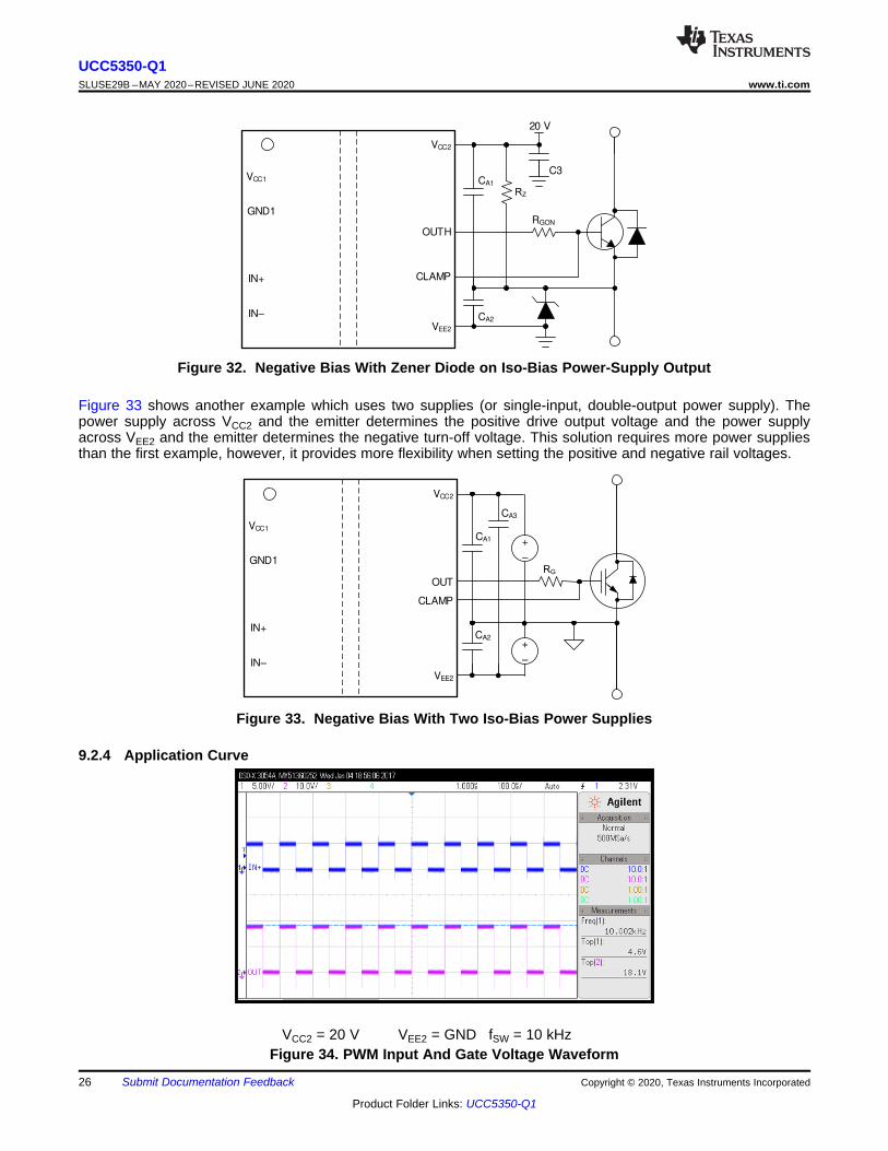
Figure 32. Negative Bias With Zener Diode on Iso-Bias Power-Supply Output
Figure 33 shows another example which uses two supplies (or single-input, double-output power supply). Thepower supply across VCC2 and the emitter determines the positive drive output voltage and the power supplyacross VEE2 and the emitter determines the negative turn-off voltage. This solution requires more power suppliesthan the first example, however, it provides more flexibility when setting the positive and negative rail voltages.
Figure 33. Negative Bias With Two Iso-Bias Power Supplies
9.2.4 Application Curve
VCC2 = 20 V VEE2 = GND fSW = 10 kHzFigure 34. PWM Input And Gate Voltage Waveform

27
UCC5350-Q1www.ti.com SLUSE29B –MAY 2020–REVISED JUNE 2020
Product Folder Links: UCC5350-Q1
Submit Documentation FeedbackCopyright © 2020, Texas Instruments Incorporated
10 Power Supply RecommendationsThe recommended input supply voltage (VCC1) for the UCC5350-Q1 device is from 3 V to 15 V. The lower limit ofthe range of output bias-supply voltage (VCC2) is determined by the internal UVLO protection feature of thedevice. The VCC1 and VCC2 voltages should not fall below their respective UVLO thresholds for normal operation,or else the gate-driver outputs can become clamped low for more than 50 μs by the UVLO protection feature. Formore information on UVLO, see the Undervoltage Lockout (UVLO) section. The higher limit of the VCC2 rangedepends on the maximum gate voltage of the power device that is driven by the UCC5350-Q1 device, andshould not exceed the recommended maximum VCC2 of 33 V. A local bypass capacitor should be placedbetween the VCC2 and VEE2 pins, with a value of 220-nF to 10-μF for device biasing. TI recommends placing anadditional 100-nF capacitor in parallel with the device biasing capacitor for high frequency filtering. Bothcapacitors should be positioned as close to the device as possible. Low-ESR, ceramic surface-mount capacitorsare recommended. Similarly, a bypass capacitor should also be placed between the VCC1 and GND1 pins. Giventhe small amount of current drawn by the logic circuitry within the input side of the UCC5350-Q1 device, thisbypass capacitor has a minimum recommended value of 100 nF.
If only a single, primary-side power supply is available in an application, isolated power can be generated for thesecondary side with the help of a transformer driver such as Texas Instruments' SN6501 or SN6505A. For suchapplications, detailed power supply design and transformer selection recommendations are available in SN6501Transformer Driver for Isolated Power Supplies data sheet and SN6505A Low-Noise 1-A Transformer Drivers forIsolated Power Supplies data sheet.
28
UCC5350-Q1SLUSE29B –MAY 2020–REVISED JUNE 2020 www.ti.com
Product Folder Links: UCC5350-Q1
Submit Documentation Feedback Copyright © 2020, Texas Instruments Incorporated
11 Layout
11.1 Layout GuidelinesDesigners must pay close attention to PCB layout to achieve optimum performance for the UCC5350-Q1. Somekey guidelines are:• Component placement:
– Low-ESR and low-ESL capacitors must be connected close to the device between the VCC1 and GND1pins and between the VCC2 and VEE2 pins to bypass noise and to support high peak currents when turningon the external power transistor.
– To avoid large negative transients on the VEE2 pins connected to the switch node, the parasiticinductances between the source of the top transistor and the source of the bottom transistor must beminimized.
• Grounding considerations:– Limiting the high peak currents that charge and discharge the transistor gates to a minimal physical area
is essential. This limitation decreases the loop inductance and minimizes noise on the gate terminals ofthe transistors. The gate driver must be placed as close as possible to the transistors.
• High-voltage considerations:– To ensure isolation performance between the primary and secondary side, avoid placing any PCB traces
or copper below the driver device. A PCB cutout or groove is recommended in order to preventcontamination that may compromise the isolation performance.
• Thermal considerations:– A large amount of power may be dissipated by the UCC5350-Q1 if the driving voltage is high, the load is
heavy, or the switching frequency is high (for more information, see the Estimate Gate-Driver Power Losssection). Proper PCB layout can help dissipate heat from the device to the PCB and minimize junction-to-board thermal impedance (θJB).
– Increasing the PCB copper connecting to the VCC2 and VEE2 pins is recommended, with priority onmaximizing the connection to VEE2. However, the previously mentioned high-voltage PCB considerationsmust be maintained.
– If the system has multiple layers, TI also recommends connecting the VCC2 and VEE2 pins to internalground or power planes through multiple vias of adequate size. These vias should be located close to theIC pins to maximize thermal conductivity. However, keep in mind that no traces or coppers from differenthigh voltage planes are overlapping.
29
UCC5350-Q1www.ti.com SLUSE29B –MAY 2020–REVISED JUNE 2020
Product Folder Links: UCC5350-Q1
Submit Documentation FeedbackCopyright © 2020, Texas Instruments Incorporated
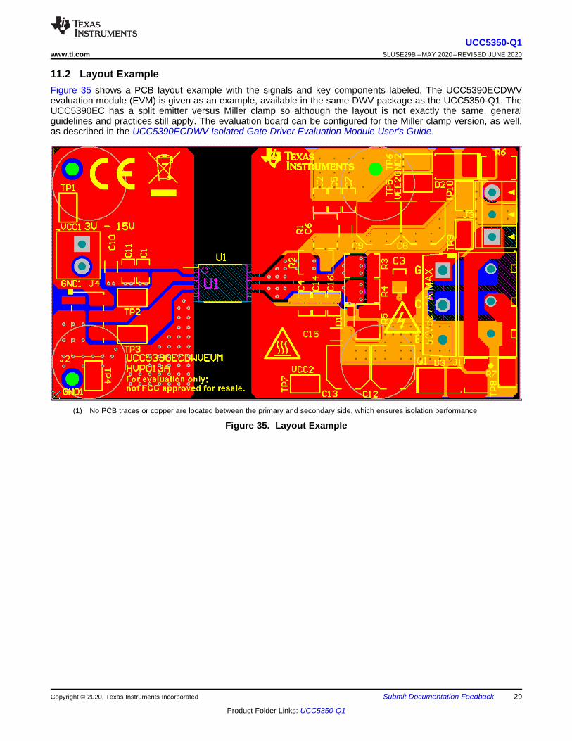
11.2 Layout ExampleFigure 35 shows a PCB layout example with the signals and key components labeled. The UCC5390ECDWVevaluation module (EVM) is given as an example, available in the same DWV package as the UCC5350-Q1. TheUCC5390EC has a split emitter versus Miller clamp so although the layout is not exactly the same, generalguidelines and practices still apply. The evaluation board can be configured for the Miller clamp version, as well,as described in the UCC5390ECDWV Isolated Gate Driver Evaluation Module User's Guide.
(1) No PCB traces or copper are located between the primary and secondary side, which ensures isolation performance.
Figure 35. Layout Example
30
UCC5350-Q1SLUSE29B –MAY 2020–REVISED JUNE 2020 www.ti.com
Product Folder Links: UCC5350-Q1
Submit Documentation Feedback Copyright © 2020, Texas Instruments Incorporated
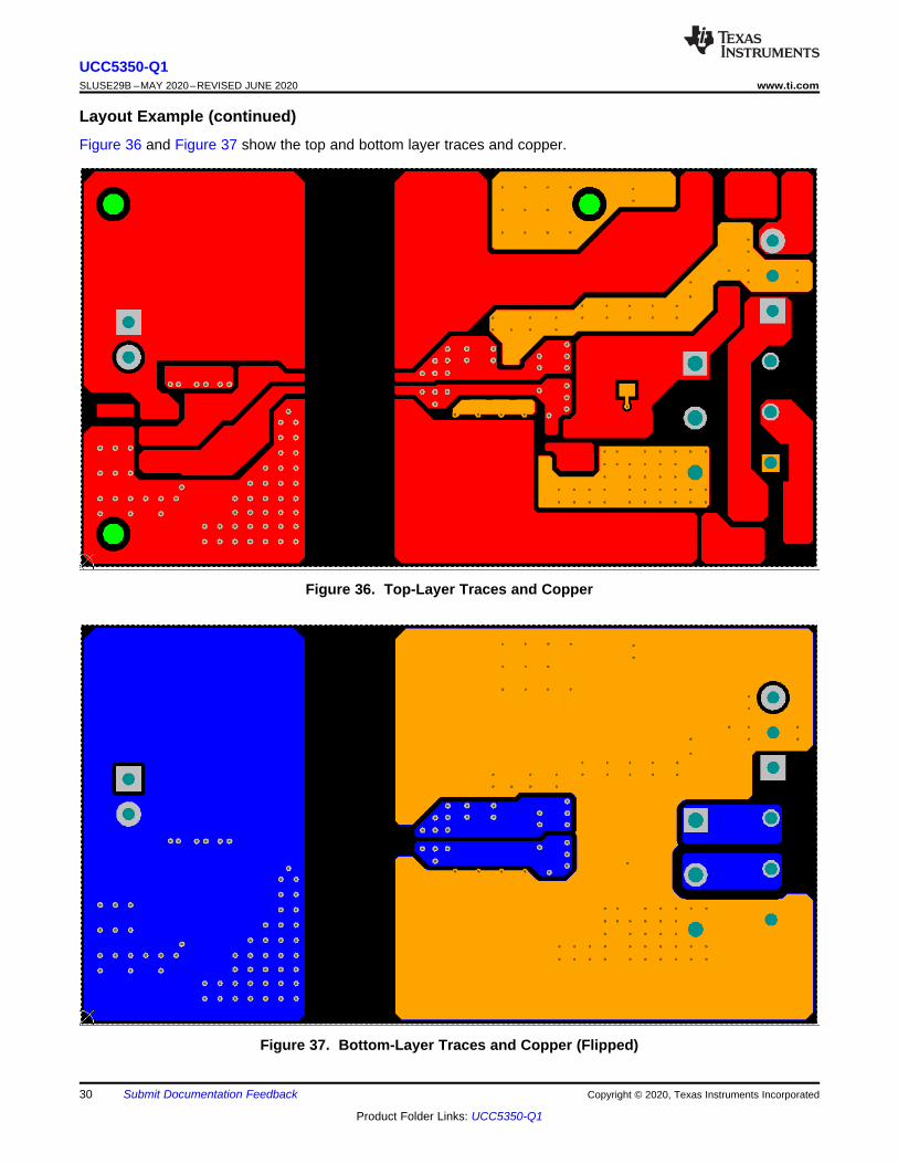
Layout Example (continued)Figure 36 and Figure 37 show the top and bottom layer traces and copper.
Figure 36. Top-Layer Traces and Copper
Figure 37. Bottom-Layer Traces and Copper (Flipped)
10 mils
10 mils
40 milsFR-4
0r ~ 4.5
Keep this space
free from planes,
traces, pads, and
vias
Ground plane
Power plane
Low-speed traces
High-speed traces
31
UCC5350-Q1www.ti.com SLUSE29B –MAY 2020–REVISED JUNE 2020
Product Folder Links: UCC5350-Q1
Submit Documentation FeedbackCopyright © 2020, Texas Instruments Incorporated
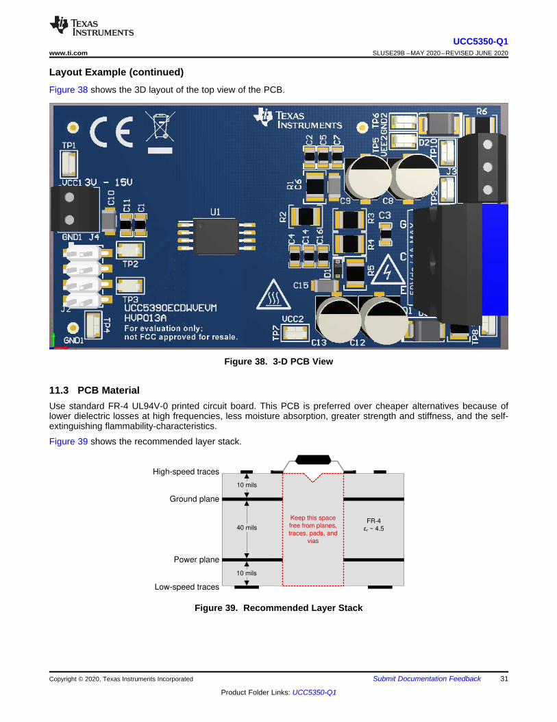
Layout Example (continued)Figure 38 shows the 3D layout of the top view of the PCB.
Figure 38. 3-D PCB View
11.3 PCB MaterialUse standard FR-4 UL94V-0 printed circuit board. This PCB is preferred over cheaper alternatives because oflower dielectric losses at high frequencies, less moisture absorption, greater strength and stiffness, and the self-extinguishing flammability-characteristics.
Figure 39 shows the recommended layer stack.
Figure 39. Recommended Layer Stack
32
UCC5350-Q1SLUSE29B –MAY 2020–REVISED JUNE 2020 www.ti.com
Product Folder Links: UCC5350-Q1
Submit Documentation Feedback Copyright © 2020, Texas Instruments Incorporated
12 Device and Documentation Support
12.1 Documentation Support
12.1.1 Related DocumentationFor related documentation see the following:• Texas Instruments, Digital Isolator Design Guide• Texas Instruments, Isolation Glossary• Texas Instruments, SN6501 Transformer Driver for Isolated Power Supplies data sheet• Texas Instruments, SN6505A Low-Noise 1-A Transformer Drivers for Isolated Power Supplies data sheet• Texas Instruments, UCC5390ECDWV Isolated Gate Driver Evaluation Module user's guide• Texas Instruments, UCC53x0xD Evaluation Module user's guide
12.2 CertificationsUL Online Certifications Directory, "FPPT2.E181974 Nonoptical Isolating Devices - Component" CertificateNumber: 20170718-E181974,
12.3 Related LinksThe table below lists quick access links. Categories include technical documents, support and communityresources, tools and software, and quick access to order now.
12.4 Receiving Notification of Documentation UpdatesTo receive notification of documentation updates, navigate to the device product folder on ti.com. In the upperright corner, click on Alert me to register and receive a weekly digest of any product information that haschanged. For change details, review the revision history included in any revised document.
12.5 Community ResourcesTI E2E™ support forums are an engineer's go-to source for fast, verified answers and design help — straightfrom the experts. Search existing answers or ask your own question to get the quick design help you need.
Linked content is provided "AS IS" by the respective contributors. They do not constitute TI specifications and donot necessarily reflect TI's views; see TI's Terms of Use.
12.6 TrademarksE2E is a trademark of Texas Instruments.All other trademarks are the property of their respective owners.
12.7 Electrostatic Discharge CautionThis integrated circuit can be damaged by ESD. Texas Instruments recommends that all integrated circuits be handled withappropriate precautions. Failure to observe proper handling and installation procedures can cause damage.
ESD damage can range from subtle performance degradation to complete device failure. Precision integrated circuits may be moresusceptible to damage because very small parametric changes could cause the device not to meet its published specifications.
12.8 GlossarySLYZ022 — TI Glossary.
This glossary lists and explains terms, acronyms, and definitions.

PACKAGE OPTION ADDENDUM
www.ti.com 10-Dec-2020
Addendum-Page 1
PACKAGING INFORMATION
Orderable Device Status(1)
Package Type PackageDrawing
Pins PackageQty
Eco Plan(2)
Lead finish/Ball material
(6)
MSL Peak Temp(3)
Op Temp (°C) Device Marking(4/5)
Samples
UCC5350MCQDQ1 ACTIVE SOIC D 8 75 RoHS & Green NIPDAU Level-2-260C-1 YEAR -40 to 125 5350Q
UCC5350MCQDRQ1 ACTIVE SOIC D 8 2500 RoHS & Green NIPDAU Level-2-260C-1 YEAR -40 to 125 5350Q
UCC5350MCQDWVQ1 ACTIVE SOIC DWV 8 64 RoHS & Green NIPDAU Level-3-260C-168 HR -40 to 125 5350MCQ
UCC5350MCQDWVRQ1 ACTIVE SOIC DWV 8 1000 RoHS & Green NIPDAU Level-3-260C-168 HR -40 to 125 5350MCQ
(1) The marketing status values are defined as follows:ACTIVE: Product device recommended for new designs.LIFEBUY: TI has announced that the device will be discontinued, and a lifetime-buy period is in effect.NRND: Not recommended for new designs. Device is in production to support existing customers, but TI does not recommend using this part in a new design.PREVIEW: Device has been announced but is not in production. Samples may or may not be available.OBSOLETE: TI has discontinued the production of the device.
(2) RoHS: TI defines "RoHS" to mean semiconductor products that are compliant with the current EU RoHS requirements for all 10 RoHS substances, including the requirement that RoHS substancedo not exceed 0.1% by weight in homogeneous materials. Where designed to be soldered at high temperatures, "RoHS" products are suitable for use in specified lead-free processes. TI mayreference these types of products as "Pb-Free".RoHS Exempt: TI defines "RoHS Exempt" to mean products that contain lead but are compliant with EU RoHS pursuant to a specific EU RoHS exemption.Green: TI defines "Green" to mean the content of Chlorine (Cl) and Bromine (Br) based flame retardants meet JS709B low halogen requirements of <=1000ppm threshold. Antimony trioxide basedflame retardants must also meet the <=1000ppm threshold requirement.
(3) MSL, Peak Temp. - The Moisture Sensitivity Level rating according to the JEDEC industry standard classifications, and peak solder temperature.
(4) There may be additional marking, which relates to the logo, the lot trace code information, or the environmental category on the device.
(5) Multiple Device Markings will be inside parentheses. Only one Device Marking contained in parentheses and separated by a "~" will appear on a device. If a line is indented then it is a continuationof the previous line and the two combined represent the entire Device Marking for that device.
(6) Lead finish/Ball material - Orderable Devices may have multiple material finish options. Finish options are separated by a vertical ruled line. Lead finish/Ball material values may wrap to twolines if the finish value exceeds the maximum column width.
Important Information and Disclaimer:The information provided on this page represents TI's knowledge and belief as of the date that it is provided. TI bases its knowledge and belief on informationprovided by third parties, and makes no representation or warranty as to the accuracy of such information. Efforts are underway to better integrate information from third parties. TI has taken and
PACKAGE OPTION ADDENDUM
www.ti.com 10-Dec-2020
Addendum-Page 2
continues to take reasonable steps to provide representative and accurate information but may not have conducted destructive testing or chemical analysis on incoming materials and chemicals.TI and TI suppliers consider certain information to be proprietary, and thus CAS numbers and other limited information may not be available for release.
In no event shall TI's liability arising out of such information exceed the total purchase price of the TI part(s) at issue in this document sold by TI to Customer on an annual basis.
OTHER QUALIFIED VERSIONS OF UCC5350-Q1 :
• Catalog: UCC5350
NOTE: Qualified Version Definitions:
• Catalog - TI's standard catalog product

www.ti.com
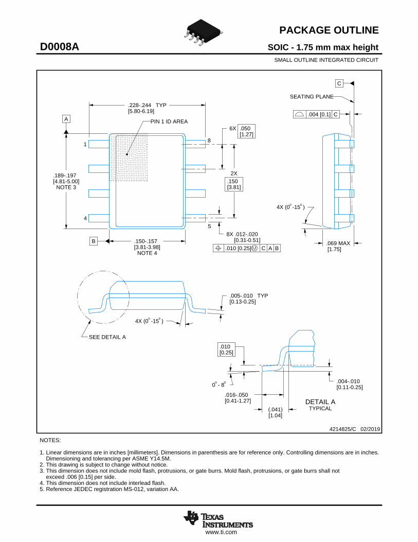
PACKAGE OUTLINE
C
TYP11.5 0.25
2.8 MAX
TYP0.330.13
0 -8
6X 1.27
8X 0.510.31
2X3.81
0.460.36
1.00.5
0.25GAGE PLANE
A
NOTE 3
5.955.75
BNOTE 4
7.67.4
(2.286)
(2)
4218796/A 09/2013
SOIC - 2.8 mm max heightDWV0008ASOIC
NOTES: 1. All linear dimensions are in millimeters. Dimensions in parenthesis are for reference only. Dimensioning and tolerancing per ASME Y14.5M. 2. This drawing is subject to change without notice. 3. This dimension does not include mold flash, protrusions, or gate burrs. Mold flash, protrusions, or gate burrs shall not exceed 0.15 mm, per side. 4. This dimension does not include interlead flash. Interlead flash shall not exceed 0.25 mm, per side.
18
0.25 C A B
54
AREAPIN 1 ID
SEATING PLANE
0.1 C
SEE DETAIL A
DETAIL ATYPICAL
SCALE 2.000
www.ti.com
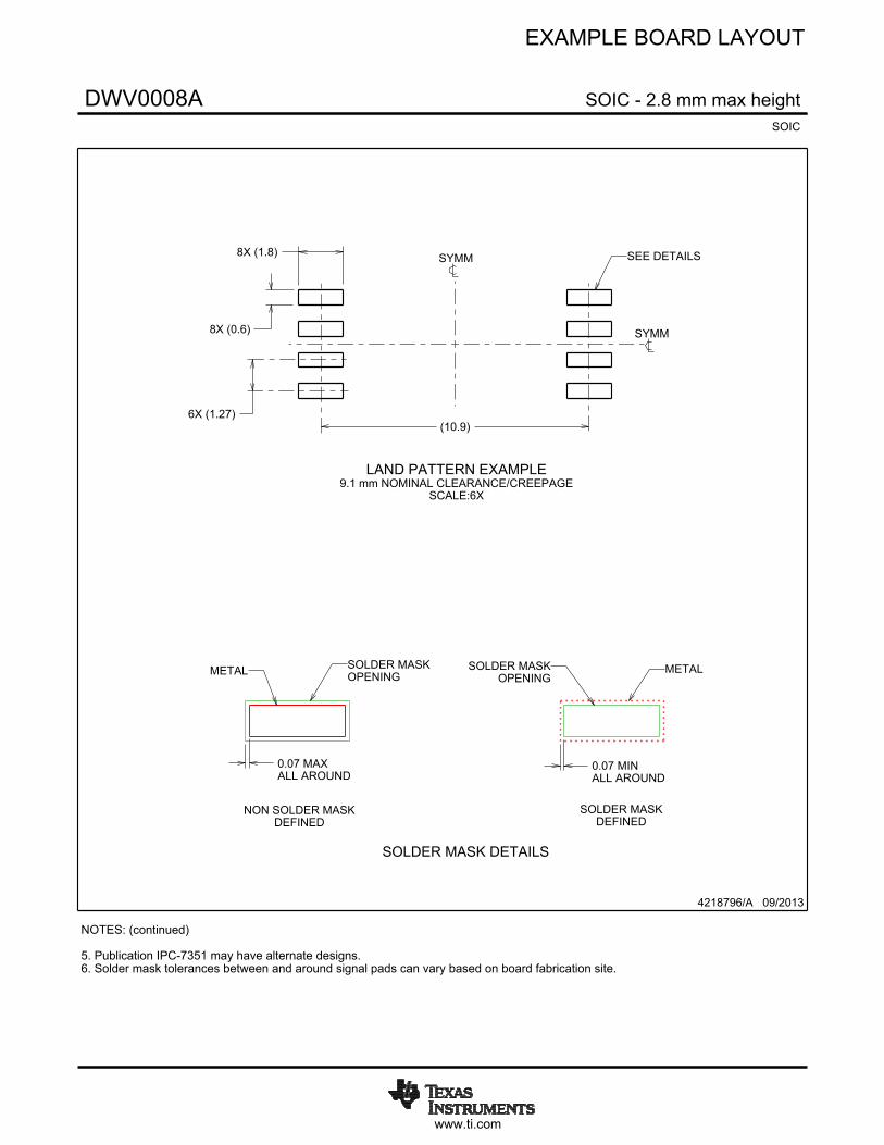
EXAMPLE BOARD LAYOUT
(10.9)
0.07 MAXALL AROUND
0.07 MINALL AROUND
8X (1.8)
8X (0.6)
6X (1.27)
4218796/A 09/2013
SOIC - 2.8 mm max heightDWV0008ASOIC
SYMM
SYMM
SEE DETAILS
LAND PATTERN EXAMPLE9.1 mm NOMINAL CLEARANCE/CREEPAGE
SCALE:6X
NOTES: (continued) 5. Publication IPC-7351 may have alternate designs. 6. Solder mask tolerances between and around signal pads can vary based on board fabrication site.
METAL SOLDER MASKOPENING
NON SOLDER MASKDEFINED
SOLDER MASK DETAILS
OPENINGSOLDER MASK METAL
SOLDER MASKDEFINED
www.ti.com
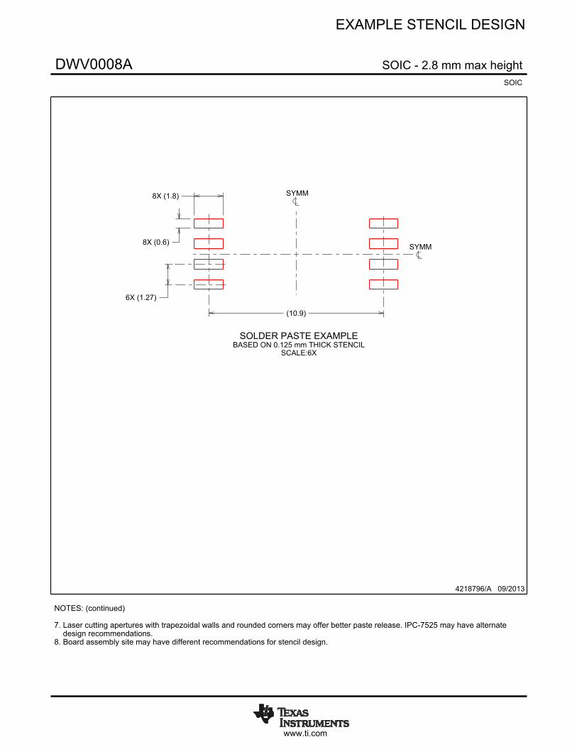
EXAMPLE STENCIL DESIGN
8X (1.8)
8X (0.6)
6X (1.27)
(10.9)
4218796/A 09/2013
SOIC - 2.8 mm max heightDWV0008ASOIC
NOTES: (continued) 7. Laser cutting apertures with trapezoidal walls and rounded corners may offer better paste release. IPC-7525 may have alternate design recommendations. 8. Board assembly site may have different recommendations for stencil design.
SOLDER PASTE EXAMPLEBASED ON 0.125 mm THICK STENCIL
SCALE:6X
SYMM
SYMM
www.ti.com
PACKAGE OUTLINE
C
.228-.244 TYP[5.80-6.19]
.069 MAX[1.75]
6X .050[1.27]
8X .012-.020 [0.31-0.51]
2X.150[3.81]
.005-.010 TYP[0.13-0.25]
0 - 8 .004-.010[0.11-0.25]
.010[0.25]
.016-.050[0.41-1.27]
4X (0 -15 )
A
.189-.197[4.81-5.00]
NOTE 3
B .150-.157[3.81-3.98]
NOTE 4
4X (0 -15 )
(.041)[1.04]
SOIC - 1.75 mm max heightD0008ASMALL OUTLINE INTEGRATED CIRCUIT
4214825/C 02/2019
NOTES: 1. Linear dimensions are in inches [millimeters]. Dimensions in parenthesis are for reference only. Controlling dimensions are in inches. Dimensioning and tolerancing per ASME Y14.5M. 2. This drawing is subject to change without notice. 3. This dimension does not include mold flash, protrusions, or gate burrs. Mold flash, protrusions, or gate burrs shall not exceed .006 [0.15] per side. 4. This dimension does not include interlead flash.5. Reference JEDEC registration MS-012, variation AA.
18
.010 [0.25] C A B
54
PIN 1 ID AREA
SEATING PLANE
.004 [0.1] C
SEE DETAIL A
DETAIL ATYPICAL
SCALE 2.800
www.ti.com
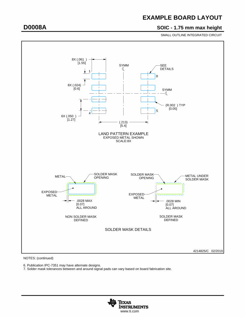
EXAMPLE BOARD LAYOUT
.0028 MAX[0.07]ALL AROUND
.0028 MIN[0.07]ALL AROUND
(.213)[5.4]
6X (.050 )[1.27]
8X (.061 )[1.55]
8X (.024)[0.6]
(R.002 ) TYP[0.05]
SOIC - 1.75 mm max heightD0008ASMALL OUTLINE INTEGRATED CIRCUIT
4214825/C 02/2019
NOTES: (continued) 6. Publication IPC-7351 may have alternate designs. 7. Solder mask tolerances between and around signal pads can vary based on board fabrication site.
METALSOLDER MASKOPENING
NON SOLDER MASKDEFINED
SOLDER MASK DETAILS
EXPOSEDMETAL
OPENINGSOLDER MASK METAL UNDER
SOLDER MASK
SOLDER MASKDEFINED
EXPOSEDMETAL
LAND PATTERN EXAMPLEEXPOSED METAL SHOWN
SCALE:8X
SYMM
1
45
8
SEEDETAILS
SYMM
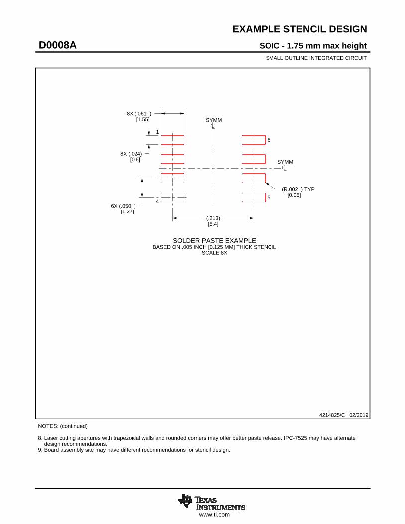
www.ti.com
EXAMPLE STENCIL DESIGN
8X (.061 )[1.55]
8X (.024)[0.6]
6X (.050 )[1.27]
(.213)[5.4]
(R.002 ) TYP[0.05]
SOIC - 1.75 mm max heightD0008ASMALL OUTLINE INTEGRATED CIRCUIT
4214825/C 02/2019
NOTES: (continued) 8. Laser cutting apertures with trapezoidal walls and rounded corners may offer better paste release. IPC-7525 may have alternate design recommendations. 9. Board assembly site may have different recommendations for stencil design.
SOLDER PASTE EXAMPLEBASED ON .005 INCH [0.125 MM] THICK STENCIL
SCALE:8X
SYMM
SYMM
1
45
8

IMPORTANT NOTICE AND DISCLAIMER
TI PROVIDES TECHNICAL AND RELIABILITY DATA (INCLUDING DATASHEETS), DESIGN RESOURCES (INCLUDING REFERENCE DESIGNS), APPLICATION OR OTHER DESIGN ADVICE, WEB TOOLS, SAFETY INFORMATION, AND OTHER RESOURCES “AS IS” AND WITH ALL FAULTS, AND DISCLAIMS ALL WARRANTIES, EXPRESS AND IMPLIED, INCLUDING WITHOUT LIMITATION ANY IMPLIED WARRANTIES OF MERCHANTABILITY, FITNESS FOR A PARTICULAR PURPOSE OR NON-INFRINGEMENT OF THIRD PARTY INTELLECTUAL PROPERTY RIGHTS.These resources are intended for skilled developers designing with TI products. You are solely responsible for (1) selecting the appropriate TI products for your application, (2) designing, validating and testing your application, and (3) ensuring your application meets applicable standards, and any other safety, security, or other requirements. These resources are subject to change without notice. TI grants you permission to use these resources only for development of an application that uses the TI products described in the resource. Other reproduction and display of these resources is prohibited. No license is granted to any other TI intellectual property right or to any third party intellectual property right. TI disclaims responsibility for, and you will fully indemnify TI and its representatives against, any claims, damages, costs, losses, and liabilities arising out of your use of these resources.TI’s products are provided subject to TI’s Terms of Sale (www.ti.com/legal/termsofsale.html) or other applicable terms available either on ti.com or provided in conjunction with such TI products. TI’s provision of these resources does not expand or otherwise alter TI’s applicable warranties or warranty disclaimers for TI products.
Mailing Address: Texas Instruments, Post Office Box 655303, Dallas, Texas 75265Copyright © 2020, Texas Instruments Incorporated