Optocoupler - HEPHY · 15 MBd Logic Gate Optocoupler ... Isolated Gate Driver for...
82
Optocoupler Designer’s Guide
Transcript of Optocoupler - HEPHY · 15 MBd Logic Gate Optocoupler ... Isolated Gate Driver for...

Optocoupler
Designer’s Guide

About This Designer’s Guide
Agilent Technologiesoptocouplers can be used in anarray of isolation applicationsranging from power supply andmotor control circuits to datacommunication and digital logicinterface circuits.
To help you choose and designwith Agilent Technologiesisolation components, thisDesigner’s Guide containspopular application circuits andrecommended Agilentoptocouplers.
This handbook begins with aselection guide followed bysections discussing criticaloptocoupler design parameterssuch as Insulation and WithstandVoltage, Regulatory AgencySafety Standards, Common-ModeTransient Rejection, Product Lifeand light emitting diode (LED)aging. The rest of the guideconsists of application circuits.
Each application circuit isaccompanied by:1. A brief description.2. Highlights of circuit
performance.3. Circuit benefits.4. A list of alternative Agilent
parts indicating comparablyperforming products availablein varying package styles formaximum design flexibility.
How to Use This Guide
Several indexes are included tohelp locate applications andproducts.• The table of contents lists all
the applications by theirgeneral description.
• Selection Guides in the form oftables contain basic productspecifications which allow youto quickly select the productsmost suitable for yourapplications.
Data sheets for productsrecommended in this guidecan be found on the AgilentTechnologies’ web site atwww.agilent.com/semiconductors,or they may be ordered from yourlocal Agilent representative.
How to Order
To order any component in thisguide or additional applicationsinformation, call your authorizedAgilent distributor nearest you.
Although product informationand illustrations in this guidewere current at the time it wasapproved for printing, AgilentTechnologies, in a continuingeffort to offer excellent productsat a fair value, reserves the rightto change specifications, designs,and models without notice.
Table of Contents
Optocoupler Selection Guide ............................................................................................... 115 MBd Logic Gate Optocoupler ................................................................................................... 21 MBd Transistor Output Optocoupler ........................................................................................ 2100 KBd Darlington Transistor Output Optocoupler ................................................................. 220 MBd Digital Logic Gate Optocoupler ...................................................................................... 310 MBd Digital Logic Gate Optocoupler ...................................................................................... 38 MBd Digital Logic Gate Optocoupler ........................................................................................ 45 MBd Digital Logic Gate Optocoupler ........................................................................................ 41 MBd Digital Transistor Output Optocoupler ............................................................................ 5100 KBd Darlington Transistor Output Optocoupler ................................................................. 5Integrated Gate Drive Optocoupler .............................................................................................. 6Miniature Analog Isolation Amplifiers ......................................................................................... 6Optocouplers with Integrated Functions ..................................................................................... 7
Hermetic and Hi-Rel Optocouplers ...................................................................................... 9For Military, Space, Life Critical and High Reliability Applications ........................................ 9Screening per MIL-PRF-38534 ..................................................................................................... 10Quality Conformance Inspection ................................................................................................ 10
Design Considerations ........................................................................................................ 13Insulation and Regulation of Optically Coupled Isolation Devices ....................................... 13Common-Mode Transient Rejection ........................................................................................... 17LED Degradation Over Time ....................................................................................................... 22Guidelines for Printed Circuit Board Assembly and Layout ................................................... 25
Digital Optoisolators: An Overview ................................................................................ 26
Digital Logic Interface/Level Shifting Applications ................................................... 28
TTL Interface with Series LED Drive ........................................................................... 28
Level Shifting/TTL Interface with Shunt LED Drive .................................................. 29
Low Power 8 MBd CMOS Interface .............................................................................. 30
25 MBd CMOS Interface ................................................................................................ 31
Low Power 100 kBd CMOS Interface ............................................................................ 32
Isolated 3 V Logic Interface/Battery Operated Applications....................................... 33
Data Communication Applications ................................................................................. 34
Isolated RS-232C/E Interface ........................................................................................ 35
Isolated 3.3 V RS-232 Interface ..................................................................................... 35
Isolated RS-485 Bus Interface ....................................................................................... 36
Isolated Device Net/CAN Communication Interface ................................................... 37

Isolated 4 - 20 mA Analog Current Loop Transmitter/Receiver ................................. 38
Isolated 20 mA Current Loop Interface ........................................................................ 39
Multidrop Line Receiver ................................................................................................. 40
Isolated Balanced Line Receiver - Circuit No. 1 ........................................................... 41
Isolated Balanced Line Receiver - Circuit No. 2 ........................................................... 42
Isolated Tri-State Line Driver ....................................................................................... 43
Isolated Unbalanced Line Receiver ............................................................................... 44
PROFIBUS/RS-422 1.5 MB/s ......................................................................................... 45
Isolated PROFIBUS/RS-485 12 MB/s Communication Application ........................... 46
Telecommunications Applications .................................................................................. 47
Telephone Ring Detection .............................................................................................. 47
ISDN Interface ................................................................................................................ 48
Analog Applications ............................................................................................................ 49
High Speed Isolation Amplifier ..................................................................................... 50
Precision Isolation Amplifier for Unipolar Signals ...................................................... 51
Isolation Amplifier for Bipolar Signals - Circuit No. 1 ................................................ 52
Isolation Amplifier for Bipolar Signals - Circuit No. 2 ................................................ 53
AC-Coupled Isolation Amplifier .................................................................................... 54
Isolated Video Interface ................................................................................................. 55
Motor Control Applications .............................................................................................. 56
Inverter Design Using Gate Drive and Current Sense Optocouplers ......................... 56
Isolated Gate Driver for IGBT/MOSFET ...................................................................... 61
Dual Channel Isolated Gate Driver for IGBT/MOSFET ............................................. 62
Isolated Gate Driver for IGBT/MOSFET with Desaturation Protection .................... 63
Isolated Interface for Intelligent Power Module Gate Drive ....................................... 64
Low Cost Isolated Phase Current Sensing with Analog Output ................................. 65
Isolated A/D Converter for Phase Current Sensing ..................................................... 66
Low Cost Isolated Phase Current Sensing
with Analog Output/Over Current Detection .......................................................... 67
Isolated Inverter Rail Voltage Sensing using an Isolation Amplifier ......................... 68
Isolated Inverter Rail Voltage Sensing using a Linear Optocoupler .......................... 69
Low Cost Isolation Amplifier for Motor Speed and Position Measurement ............... 70
Industrial Applications ...................................................................................................... 71
AC/DC Voltage Threshold Sensing ................................................................................ 71
Optical Isolation in Flat-Panel Displays ....................................................................... 72
Power Supply Applications ............................................................................................... 73
Optical Isolation in a Switching Power Supply - Circuit No. 1 ................................... 73
Optical Isolation in a Switching Power Supply - Circuit No. 2 ................................... 74
Optical Isolation in a DC/DC Converter ....................................................................... 75
Application Notes ................................................................................................................ 76

Agilent Technologies offers a
broad range of isolation
products which provide
performance features and
benefits that are unmatched in
the industry. Some of the
leading product performance
technologies that Agilent offers
include:
• Dielectric Withstand Voltage
Rating as high as 5000 Vac/1
min (per UL)
• First 3.3V optocoupler in the
world
• Phototransistor optocouplers
• Worldwide Safety Approvals,
including the highest
Maximum Working
Insulation Voltage (VIORM) at
1000 V (per VDE)
• Common-Mode Transient
Noise Immunity as high as 15
kV/µs (Minimum)
• A wide variety of surface
mount and multi-channel
packages, including the
highest density optocouplers
in the world.
• Lowest power dissipation
optocouplers available, with
input currents as low as 40
µA
• Highest speed optocouplers,
with data rates as high as
25 MBd and propagation
delays as low as 40 ns
• Wide operating temperatureranges for industrial and
military environments
• A full line of hermetically-
sealed optocouplers for high
reliability applications.
Available as commercial
grade or Certified and
Qualified to MIL-PRF-38534
Class H or K. DSCC
Standard Microcircuit
Drawings (SMDs) are
available on all hermetic
products.
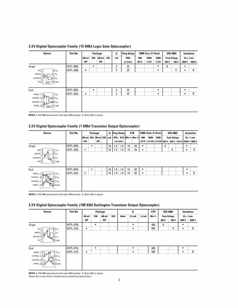
Optocoupler Selection Guide
2
NOTES: A. VDE 0884 approved part with option 060 (pending). B. Option 020 on request.
Dual
SingleVCCNC
NC
ANODE
CATHODE
VE
SHIELD
VO
GND
8
76
5
1
2
34
VCCANODE
ANODE
CATHODE
CATHODE
VO11
1
2
2 SHIELD
VO2
GND
8
76
5
12
34
Insulation
560 V
Peak Voltage
VDE 0884CMR-V/µs @ (Vcm)IƒPackagePart No. Prop Delay
630 V 2500 V
UL = 1 min.
5000 V
300 mil
DIP
SO8 400 mil
DIP
PWD
ns (max)
1000
(50 V)
10000
(1 kV)
15000
(1 kV)
mASO5
• ••
••
55
2525
AA B•
HCPL-060LHCPL-260L
• ••
••
55
2525 B•
HCPL-063LHCPL-263L
Device
3.3V Digital Optocoupler Family (15 MBd Logic Gate Optocoupler)
NOTES: A. VDE 0884 approved part with option 060 (pending). B. Option 020 on request.
Dual
SingleVCCNC
NC
ANODE
CATHODE
VE
VO
GND
87
6
5
1
2
34
VCCANODE
ANODE
CATHODE
CATHODE
VO1
VO2
1
1
2
2 GND
8
7
6
5
12
3
4
Insulation
560 V
Peak Voltage
VDE 0884CMR-V/ms @ (Vcm)IƒPackagePart No. Prop Delay
630 V 1414 V 2500 V
UL = 1 min.
5000 V
300 mil
DIP
SO8 400 mil
DIP
tPHL 1000
(10 V)
10000
(1.5 kV)
15000
(1.5 kV)
mASO5
HCPL-050LHCPL-250L
HCPL-053LHCPL-253L
Device
tPLH
CTR
Min % Max %
• ••
••
1616
1.01.0
AA B•
• ••
••
1616
1.01.0
1.01.0
1.01.0 B•
1919
5050
1919
5050
ms (max)
3.3V Digital Optocoupler Family (1 MBd Transistor Output Optocoupler)
NOTES: A. VDE 0884 approved part with option 060 (pending). B. Option 020 on request.Please refer to data sheet for detailed electrical/switching specifications.
Dual
SingleVCCNC
NC
ANODE
CATHODE
VE
VO
GND
8
76
5
1
23
4
VCCANODE
ANODE
CATHODE
CATHODE
VO1
VO2
1
1
2
2 GND
8
7
6
5
1
2
34
• AA B•
•
••
••
•• B•
400400
400400
300 mil
DIP 560 V
Peak Voltage
630 V 2500 V
UL = 1 min.
5000 V
SO8 400 mil
DIP
40mA 0.5 mASO5 Min %1.6 mA
InsulationVDE 0884IƒPackagePart No.
••
HCPL-070LHCPL-270L
HCPL-073LHCPL-273L
Device CTR
3.3V Digital Optocoupler Family (100 KBd Darlington Transistor Output Optocoupler)

3
Single
V
VEAnode
Cathode V
8
7
6
5
1
2
3
4
CC
OUT
GND
Dual
CCV
V01
Anode1
Cathode1
Cathode2
Anode2
V02
8
7
6
5
1
2
3
4
Shaded Text–RECOMMENDED FOR NEW DESIGNS NOTES: 2. 630 V peak VDE 0884 with option 060. B. Option 020
6N137HCPL-0600HCNW137HCPL-M600HCPL-2601
HCNW2601HCPL-M601HCPL-2611
HCPL-061NHCPL-261NHCPL-061AHCPL-261AHCNW2611 HCPL-M611HCPL-0611
HCPL-0601
HCPL-0630HCPL-2631HCPL-0631
HCPL-0661HCPL-263AHCPL-063A
HCPL-063NHCPL-263N
HCPL-4661
HCPL-2630
Insulation Note
2500 V UL = 1 min.
5000 V630 V
Peak Voltage
1414 V
VDE 0884CMR-V/ms @ (Vcm)
5000
(50 V)
10000
(200 V)
10000
(1 kV)
15000
(1 kV)
1000
(50 V)
tPHL/tPLH
ns (max)
Prop Delay
mA
Iƒ
300 mil
DIP
400 mil
DIP
SO8 SO5
PackageDevice Part No.
• 5 100•
•
•
•
•
•
••
••
•
••
•
•
555555555552222
100100100100100100100100100100100100100100100
• •
••
•
•••
•••
••••
••
••
••
••
••
•
1005100510051005100510051005100510021002
••
••
•
••
• B
•••
•
•• •
B
B
2
B 2
B 2
•• •
•
• ••••
•
•
••••
•• B
B
B
B
B••••
10 MBd Digital Logic Gate Optocoupler
20 MBd Digital Logic Gate Optocoupler
CC
Cathode
Cathode
GND
V
V01
Anode1
1
2
Anode2
V02
8
7
6
5
1
2
3
4
Single
DualHCPL-2430
HCPL-2400
Anode
Cathode
Anode1
8
7
6
5
2
3
4
NC
NC
VE
VD
VCC
GND
HCPL-2400 • 4 60 • • • 2
HCPL-2430 • 60 • •4
Insulation Note
2500 V UL = 1 min.
5000 V630 V
Peak Voltage 1414 V
VDE 0884CMR-V/µs @ (Vcm)
2000
(200 V)
5000
(50 V)
10000
(200 V)
10000
(1 kV)
15000
(1 kV)
1000
(50 V)
tPHL/tPLH
ns (max)
Prop Delay
mA
Iƒ
300 mil
DIP
400 mil
DIP
SO8 SO5
PackageDevice Part No.
NOTES: 2. 630 V peak VDE 0884 with option 060.

4
Single
HCPL-0211HCNW2211 1.6 4•
HCPL-2200 • 1.6 2HCPL-2219 • 1.6 2HCPL-2201 • 1.6 2, 4HCPL-2202 • 1.6 2, 4, 5HCPL-0201 • 1.6 4HCNW2201 • 1.6 4HCPL-2211 • 1.6 2, 4HCPL-2212 • 1.6 2, 4, 5
• 1.6 4
••
• •
•
•
••
•
••••
••
•
HCPL-2231 • 1.8HCPL-2232 • 1.8
••
•• 6
Dual• •
•
VCC
VOUTAnode
Cathode VE
GND
8
7
6
5
1
2
3
4
7
1
2
3
4 5
6
8ANODE 1
CATHODE 1
CATHODE 2
VCC
VO1
VO2
GNDANODE 2
Shaded Text–RECOMMENDED FOR NEW DESIGNS NOTES: 2. 630 V peak VDE 0884 with option 060. 4. PIN 7 not connected. 5. PINS 6 and 7 reversed. 6. CMR=5000
Insulation Note
2500 V
UL = 1 min.
630 V
Peak Voltage
VDE 0884CMR-V/µs @ (Vcm)IƒPackageDevice Part No.
300 mil
DIPSO8 400 mil
DIPmA 10000
(1 kV)
2500
(1400 V)
1000
(50 V) 5000 V1414 V
5 MBd Digital Logic Gate Optocoupler
8 MBd Digital Logic Gate Optocoupler
Single
1
4
8
7
6
5
VCC
VD
RL
GND
23
Anode
Cathode
NOTES: 2. 630 V peak VDE 0884 with option 060.
•HCPL-2300 ••
0.50.5
••
•• •
2
Insulation Note
2500 V UL = 1 min.
5000 V630 V
Peak Voltage 1414 V
VDE 0884CMR-V/ms @ (Vcm)IƒPackageDevice Part No.
300 mil
DIPSO8 400 mil
DIP
mA SO5 100
(50 V)
1000
(50 V) 2500
(1400 V)
10000
(1 kV)
HCPL-0300
5
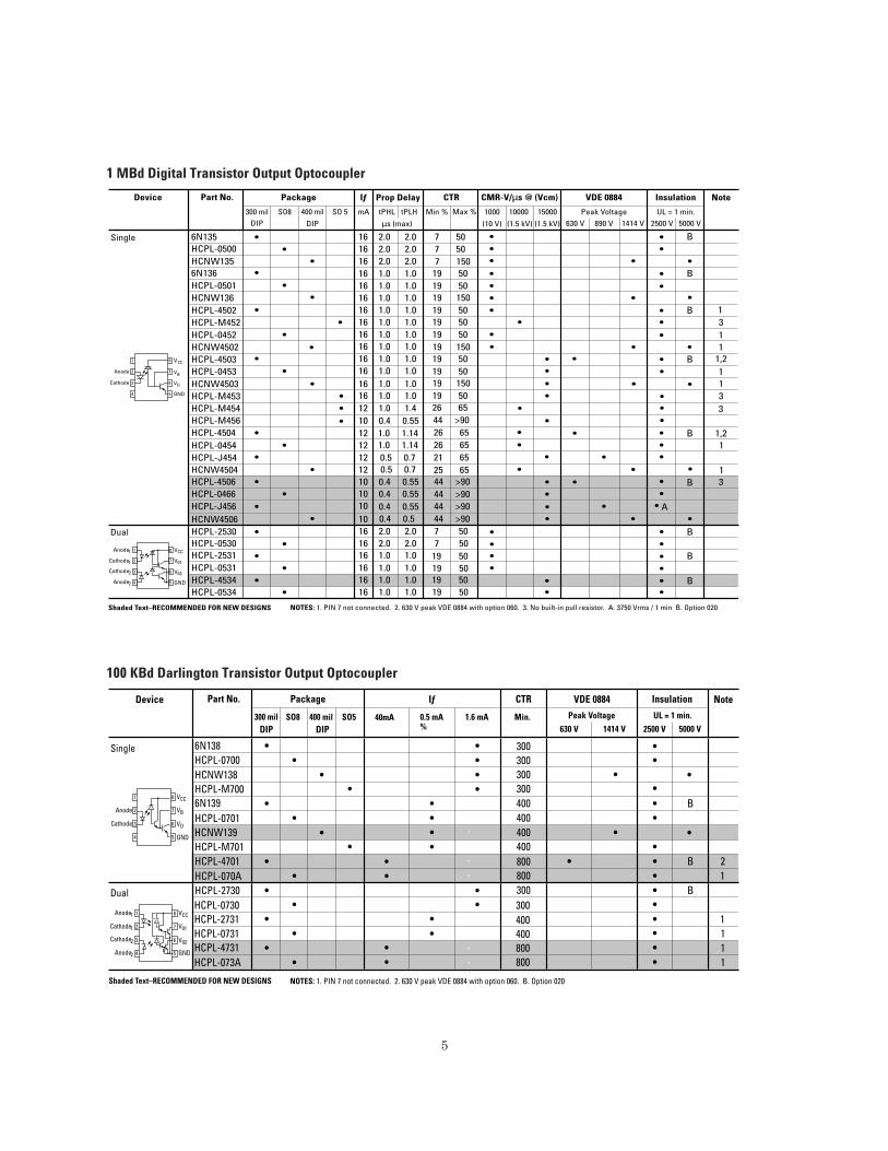
1 MBd Digital Transistor Output Optocoupler
Dual
Single
V
VAnode
Cathode V
GND
8
7
6
5
1
2
3
4
CC
B
O
VCC
V01
Anode1
Cathode1
Cathode2
Anode2
V02
GND
8
7
6
5
1
2
3
4
Shaded Text–RECOMMENDED FOR NEW DESIGNS NOTES: 1. PIN 7 not connected. 2. 630 V peak VDE 0884 with option 060. 3. No built-in pull resistor. A. 3750 Vrms / 1 min B. Option 020
6N135HCPL-0500HCNW1356N136HCPL-0501
HCPL-4502HCPL-M452HCPL-0452
HCPL-4504
HCNW4506
HCPL-M456HCPL-M454HCPL-M453HCNW4503HCPL-0453HCPL-4503
HCPL-0454
HCNW4502
HCNW136
HCPL-J456HCPL-0466HCPL-4506HCNW4504HCPL-J454
HCPL-0530HCPL-2531HCPL-0531HCPL-4534HCPL-0534
HCPL-2530
Insulation Note
2500 V UL = 1 min.
5000 V630 V Peak Voltage
1414 V
VDE 0884CMR-V/µs @ (Vcm)CTR
Max % 1000
(10 V)
10000
(1.5 kV)
15000
(1.5 kV)
Min %tPHL tPLH
µs (max)
Prop Delay
mA
Iƒ
300 milDIP
400 mil
DIP
SO8 SO 5
PackageDevice Part No.
890 V
16 2.0 2.0 7 50
19 50
19 150
26 6544 >90
44 >90
26 65
19 50
19 5019 50
19 5019 50
19 50
19 150
19 507 1507 50
19 150
16161616161616161616
16
10
16
16121012
2.0 2.02.0 2.01.0 1.01.0 1.01.0 1.01.0 1.01.0 1.01.0 1.01.0 1.01.0 1.0
1.0 1.14
0.4 0.5
1.0 1.01.0 1.01.0 1.01.0 1.40.4 0.551.0 1.14
21 6526 65
44 >90
44 >9044 >90
25 6512
101010
12 0.5 0.70.4 0.550.4 0.550.4 0.55
12
162.0 2.01.0 1.01.0 1.016
162.0 2.016
16 1.0 1.016 1.0 1.0
7
19
19 50501950501950507
0.5 0.7
•
••
••
B
••
••••••
••
•
••
•
• •
1
•
••
•
•
•
•
••
•
•
••
•
•
••
•
•
B
11
B
1
13
1
B
B
33
1,2
1,2• •
••
•
••
••
•
•
•• 1
••
••
B 3•
• A
•
••
•
••
•••••• B
B
B
••
•
•
•
•
•
•
•
••
•
•
•
•
•
•
••
•
•
•
•
•
••
•
••
•
100 KBd Darlington Transistor Output Optocoupler
Single
Dual
VCC
VBAnode
Cathode VO
GND
8
7
6
5
1
2
3
4
GND
VCC
V01
Anode1
Cathode1
Cathode2
Anode2
V02
8
7
6
5
1
2
3
4
Shaded Text–RECOMMENDED FOR NEW DESIGNS NOTES: 1. PIN 7 not connected. 2. 630 V peak VDE 0884 with option 060. B. Option 020
HCPL-4701
HCPL-2731HCPL-0731HCPL-4731HCPL-073A
6N138HCPL-0700HCNW138
6N139HCPL-0701
HCPL-M700
HCPL-M701
HCPL-070AHCPL-2730
300 mil SO8 400 mil 40mA 0.5 mA 1.6 mA Min. %
Insulation Note
2500 V UL = 1 min.
5000 V630 V
Peak Voltage 1414 V
VDE 0884CTRIƒPackageDevice Part No.
DIP DIPSO5
HCNW139
300300300300400400400400800800300
••••
•
•
•
••
•
••
•
••
••
••
•300400400800800
•••
••
••
••
•
••
••
B•
•2
B
B••
•
•
••
•
•
•
1
• 1• 1• 1
1•
•
•
HCPL-0730

6
Motor Drive Application
Gate DriveHCPL-31XXHCPL-450X
Current SenseHCPL-78XX
Current SenseHCPL-78XX
Motor
Voltage SenseHCPL-78XX
3 phase
Serial
Communication
line input
-HV
HCPL-XXXX
+HV
Controller
Integrated Gate Drive Optocoupler
Miniature Analog Isolation Amplifiers
VE
VEEVEE
COLLVCC2
VOUT
VIN+VIN-
VLED1+
VLED2+VDESAT
VLED1-
VCC1GND1
RESETFAULT
VCC
VOAnode
Cathode VO
VEE
8
7
6
5
1
2
3
4
Shaded Text–RECOMMENDED FOR NEW DESIGNS NOTES: 2. 630 V peak VDE 0884 with option 060.
812
0.6HCPL-3000HCPL-3100HCPL-3101HCPL-T250HCPL-3120HCPL-J312HCNW3120HCPL-3150
300 mil
DIP
SO16SO8400 mil
DIP
mA A
min 0.5
tPHL µs (max) 0.3 µs
max
0.8 µs
max21 5
V
max 630 V
Peak Voltage
890 V 1414 V8000
(1500)
10000
(600)
15000
(1500)
Device Part No. Package Iƒ (on) Iout Prop Delay PWD Vcc VDE 0884 CMR-V/µs @ (Vcm) Note
7
777
0.1
1.5
22
0.5
8
7 2
0.1
0.7
10 0.4HCPL-314J
HCPL-J314 10 0.4
16 0.5
1µA 2
HCPL-315J
HCPL-316J
HCPL-0314 8 0.40.40.4
HCPL-3140 8HCPL-T251 8
(1000)
•
•
• •• 18
2
••
•
••
•
•2
•
•
24
30
3030
30
•
•
••
•
•••
•
••
•
•
•
•
• •
• 24
30 • ••
• • 30 • •
•• 30 • •
•
30
30 ••••
• • • ••Dual 0.4 A Gate Drive Optocoupler with two separated channels
Dual 0.5 A Gate Drive Optocoupler with two separated channels
2.0 A Gate Drive Optocoupler with integrated over-current Protection and Fault Feedback
• CMOS compatible• Under Voltage Lock-Out Protection (UVLO) with Hysteresis• Regulatory Approvals: UL, CSA, VDE = 890 Vpeak
•
••
•
• 30 •••• 30 ••
• 30 ••
(1500)
VDD2VDD1
GND1
VIN+
VIN+
VIN-
VIN-
VOUT+
Shield
IDD2IDD1
VOUT-
GND2
8
7
6
5
1
2
3
4
+
–
+
–
12345678
161514131211109
Shaded Text–RECOMMENDED FOR NEW DESIGNS NOTES: 7. 890 V peak VDE 0884 with option 060. 8. HCPL-7800A with 1% Gain Tolerance.
CHCL
VDD1
VDD1 VDD2
VDD2
VREFVOUTABSVALFAULT
GND1 GND2
GND2
VLED+
0.40 9.9
Note
630 V
Peak Voltage
1414 V
VDE 0884 CMR-V/µs @ (Vcm)Non-LinearityPackagePart No. Gain Toler. Prop Delay
890 V
300 mil
DIP
SO16 3% 10000
(1000)
% (max) ms max5%
4.1 200.20
• ••
••
••
••
87
•••
•• • • • •
Isolated 12 bit A/D Converter with Isolated ModulatorIsolated 12 bit A/D Converter with Isolated Modulator with better creepage and clearance
HCPL-7800HCPL-7840HCPL-7860HCPL-786J
• Smart Current Sensor with integrated fast short circuit detection (3µs)• Analog Output direct compatible with A/D converters• 1 µV/ ˚C offset change vs temperature• 16 kHz bandwidth• 2500 Vac UL approval, VDE = 890 Vpeak
Device
HCPL-788J
•
•

7
Optocouplers with Integrated Functions
Wideband Analog/Video
AC/DC to Logic Interface
Line Receiver
GND
K1
LED Cathode
LED Anode
PD Cathode
PD Anode
VO
8
7
6
5
1
2
3
4
Shaded Text–RECOMMENDED FOR NEW DESIGNS
• -65 ppm/C gain temperature coefficient• 1.5 MHz bandwidth• 1 kV VDE (option 050), 5000 Vac UL Approval
HCNR200HCNR201
• 0.750.72
0.250.36
+/-15+/-5
0.250.05•
DC Non-Linearity CTRDevice Part No. Package
min % max %400 milDIP
max %
Transfer Gain
max %
VDD2
IO
NC
VDD1
Shield
V1
GND1
V0
GND2
8
7
6
5
1
2
3
4
Shaded Text–RECOMMENDED FOR NEW DESIGNS
PWD Prop DelayDevice Part No. Package
ns (max)
300 milDIP
S08
Data Rate
Mb/s 8 ns(max)
30 ns(max)
• 10 kV/µs CMR @ Vcm = 1000 V• Viorm = 630 V VDE, 3750 Vac UL Approval
12.5HCPL-7710HCPL-7720
• 40•
HCPL-7721HCPL-0710HCPL-0720HCPL-0721
25• •25• •
12.5 •25 •25• •
••
4040404040
HCPL-0708 15• • 40
6 ns(max)
• UL Approval — 5000 V rms for 1 min for HCPL-4562 option 020• 0.3%/ ˚C gain temperature coefficient
VCC
VBAnode
Cathode VO
GND
8
7
6
5
1
2
3
4
HCPL-4562HCNW4562
• 0.250.15•
179
122119 •
DC Non-Linearity CTRDevice Part No. Package
typ % Viorm
1414 Vp
400 mil
DIP
max %300 mil
DIP
IMRR VDE 0884
typ
MHz
typ
dB
Bandwidth
4552
VCCDCin+
ACin
ACin
DCin-
VO
GND
8
7
6
5
1
2
3
4
Shaded Text–RECOMMENDED FOR NEW DESIGNS
• CMOS compatible output• 600 V/µs CMR @ Vcm = 150 V• 2500 Vac UL Approval
Prop DelayHysteresisPart No. Input Threshold Current
1.20.6
mA
(typ)
ms
(max)
mA
(min)
mA
(max)
HCPL-3700HCPL-3760
1.961.56 400.873.11 40
Package
300 mil
DIP
••
Device
High Speed Digital CMOS Logic Gate
High Linearity Analog
8
7
6
5
VCC
VE+IN
-IN VOut
GND
1
2
3
4
Prop Delay CMR-V/µs @ (Vcm)Device Part No.
1000
(150)
3500
(300)
Output Collector Current
mA
(max)
ns
(max)
300 mil
DIP
Package
• 40 ns max propagation delay skew (part to part)• Line termination circuitry included• 2500 Vac UL approval
HCPL-2602HCPL-2612
••
100100
5050
••

8
300 mil8-pin DIP
400 mil8-pin DIP
4-pin DIP 6-pin DIP SO-4
Packages
Option Nomenclatures060 = VDE0884 OptionW00 = 0.4” Lead Spacing Option300 = Lead Bend SMD Option500 = Tape and Reel Packaging Option00A = Rank Mark A (for HCPL-181 and HCPL-817 only)00B = Rank Mark B (for HCPL-181 and HCPL-817 only)
”Widebody”Package
SO-5 SO 8 SO 16
SMDPackage
SMDPackage
4 3
1 2
6 45
21 3
Optocouplers with Integrated Functions, continued
20 mA Current Loop Transmitter/Receiver
1.6HCPL-4100 HCPL-4200
VCC
I+
I-
VI
GND
8
7
6
5
1
2
3
4
VCC
VO
I+
I-
VE
GND
8
7
6
5
1
2
3
4
Shaded Text–RECOMMENDED FOR NEW DESIGNS
• CMOS compatible data input for HCPL-4100• CMOS compatible data input for HCPL-4200• 2500 Vac UL approval
CMR-V/µs @ (Vcm)Prop DelayPart No. Data Rate – kBd @ (meters)
1.6
1000
(150)
ms
(max)
1000
(50)
20
400
HCPL-4100HCPL-4200
•
Device Package
20
1400
••
•••
300 mil
DIP
General Purpose Phototransistor Optocoupler
Insulation Note
3750 V<3750 V UL = 1 min.
5000 VMin V
V(BR)CEOCTRMax %Min %300 mil
DIP400 mil
DIPSO4
PackageDevice Part No.
Single Channel4 pin
Single Channel6 pin
Base
Collector
Emitter
Anode
Cathode
6
5
4
1
2
3
Anode
Cathode
4
3
1
2
NOTES: 1. VDE 0884 with option 060. A. Wide-lead spacing (10.16 mm) with option W00
Collector
Emitter
HCPL-817HCPL-817-00LHCPL-817-00AHCPL-817-00BHCPL-817-00CHCPL-817-00DHCPL-181HCPL-181-00AHCPL-181-00BHCPL-181-00CHCPL-181-00D4N254N35CNY17-1CNY17-2CNY17-3CNY17-4
505080
130200300
5080
130200300
20100
4063
100160
600100160260400600600160260400600
80125200320
3535353535353535353535707070707070
11111111111111111
••••••
••••••
••••••
••••
AAAAAA
AAAAAA
•••••
••
•••••
00C = Rank Mark C (for HCPL-181 and HCPL-817 only)00D = Rank Mark D (for HCPL-181 and HCPL-817 only)00L = Rank Mark L (for HCPL-817 only)020 = UL 5000 Vrms/1 minute OptionVDE option (060)

Hermetic and Hi-Rel Optocouplers
Choose from Agilent
Technologies’s broad line of high
performance hermetic
optocouplers to meet your
military, space, life critical, and
high reliability applications.
There are four ceramic package
styles to choose from: 8 and
16Cpin Dual-In-line Packages,
20Cterminal Leadless Ceramic
Chip Carriers, and 16 pin Flat
Pack packages. Available in most
package styles are seven basic
families of optocouplers: Analog
Isolation Amplifier, Power
Transistor Interface, High Speed
Logic Gate Optocouplers, High
Speed Transistor Optocouplers,
High Gain Optocouplers, AC/DC
to Logic Interface, and the Power
MOSFET.
Agilent Technologies hermetic
optocouplers are classified by the
Department of Defense as hybrid
microcircuits and are manufac-
tured in Singapore on a MIL-PRF-
38534 certified and qualified line.
For Military, Space, Life Critical andHigh Reliability Applications
Agilent Technologies is listed as a
qualified supplier for Classes H,
E, and K product on the Qualified
Manufactures List, QML-38534.
All product families are repre-
sented by commercial grade units
and by high reliability tested
units. To give maximum opportu-
nity to utilize recognized DSCC
parts, all 28 hermetic products
are available on DSCC Standard
Microcircuit Drawings (SMDs).
Dual part marking of the Agilent
part number and the DSCC
Drawing is standard on all high
reliability products. Each high re-
liability device is tested and guar-
anteed over the full military
temperature range of -55°C to
+125°C.
Agilent offers a standard line of
Class K devices to be procured
that require no source control
drawing to be generated. Note
that while Agilent does not cur-
rently supply a certified Class K
MOSFET or Analog Isolation
Amplifier device, we can provide
up-screening to most of the
ClassCK requirements of
MIL-PRF-38534.
Agilent Technologies is both
DSCC certified and qualified to
manufacture Class H (military
approved) and Class K (space
approved) hermetic optocouplers
per the requirements of MIL-PRF-
38534 Option 1 QCI (in-line
inspection) or Option 2 (end-of-
line inspection). All catalog Class
H devices are processed per
Option 1 QCI. Class K devices are
processed per Option 2 QCI.
Custom devices are available
processed to either option.
10
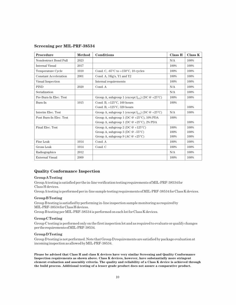
Screening per MIL-PRF-38534
Procedure Method Conditions Class H Class K
Nondestruct Bond Pull 2023 N/A 100%
Internal Visual 2017 100% 100%
Temperature Cycle 1010 Cond. C, -65°C to +150°C, 10 cycles 100% 100%
Constant Acceleration 2001 Cond. A, 3Kg’s, Y1 and Y2 100% 100%
Visual Inspection Internal requirements 100% 100%
PIND 2020 Cond. A N/A 100%
Serialization N/A 100%
Pre-Burn-In Elec. Test Group A, subgroup 1 (except II-O) (DC @ +25°C) 100% 100%
Burn-In 1015 Cond. B, +125°C, 160 hours 100%
Cond. B, +125°C, 320 hours 100%
Interim Elec. Test Group A, subgroup 1 (except II-O) (DC @ +25°C) N/A 100%
Post Burn-In Elec. Test Group A, subgroup 1 (DC @ +25°C), 10% PDA 100%
Group A, subgroup 1 (DC @ +25°C), 2% PDA 100%
Final Elec. Test Group A, subgroup 2 (DC @ +125°C) 100% 100%
Group A, subgroup 3 (DC @ –55°C) 100% 100%
Group A, subgroup 9 (AC @ +25°C) 100% 100%
Fine Leak 1014 Cond. A 100% 100%
Gross Leak 1014 Cond. C 100% 100%
Radiographics 2012 N/A 100%
External Visual 2009 100% 100%
Quality Conformance Inspection
Group A Testing
Group A testing is satisfied per the in-line verification testing requirements of MIL-PRF-38534 for
Class H devices.
Group A testing is performed per in-line sample testing requirements of MIL-PRF-38534 for Class K devices.
Group B Testing
Group B testing is satisfied by performing in-line inspection sample monitoring as required by
MIL-PRF-38534 for Class H devices.
Group B testing per MIL-PRF-38534 is performed on each lot for Class K devices.
Group C Testing
Group C testing is performed only on the first inspection lot and as required to evaluate or qualify changes
per the requirements of MIL-PRF-38534.
Group D Testing
Group D testing is not performed. Note that Group D requirements are satisfied by package evaluation at
incoming inspection as allowed by MIL-PRF-38534.
Please be advised that Class H and class K devices have very similar Screening and Quality Conformance
Inspection requirements as shown above. Class K devices, however, have substantially more stringent
element evaluation and assembly criteria. The quality and reliability of a Class K device is achieved through
the build process. Additional testing of a lesser grade product does not assure a comparative product.

11
Hermetically Sealed High Speed Logic Gate OptocouplersSingle Part No. Class H DSCC Class K DSCC Package No. Typical Common Input WithstandChannel SMD SMD 8 pin 16 pin 16 pin 20 pad of Data Mode @ Current TestSchematic Class H* Class K* DIP DIP FP LCCC Channels Rate VCM = 50V Voltage
HCPL-5200 HCPL-5201 5962-8876801 HCPL-520K 5962-8876802K • 1 5 MBd 1000V/µs 2–8 mA 1500 Vdc
HCPL-5230 HCPL-5231 5962-8876901 HCPL-523K 5962-8876904K • 2 5 MBd 1000V/µs 2–8 mA 1500 Vdc
HCPL-6230 HCPL-6231 5962-8876902 HCPL-623K 5962-8876905K • 2 5 MBd 1000V/µs 2–8 mA 1500 Vdc
HCPL-6250 HCPL-6251 5962-8876903 HCPL-625K 5962-8876906K • 4 5 MBd 1000V/µs 2–8 mA 1500 Vdc
HCPL-5400 HCPL-5401 5962-8957001 HCPL-540K 5962-8957002K • 1 20 MBd 500V/µs 6–10 mA 1500 VdcHCPL-5430 HCPL-5431 5962-8957101 HCPL-543K 5962-8957103K • 2 20 MBd 500V/µs 6–10 mA 1500 Vdc
HCPL-6430 HCPL-6431 5962-8957102 HCPL-643K 5962-8957104K • 2 20 MBd 500V/µs 6–10 mA 1500 Vdc
6N134 6N134/883B 8102801 HCPL-268K 5962-9800101K • 2 10 MBd 1000V/µs 10 mA 1500 VdcHCPL-5600 HCPL-5601 5962-9085501H HCPL-560K 5962-9085501K • 1 10 MBd 1000V/µs 10 mA 1500 Vdc
HCPL-5630 HCPL-5631 8102802 HCPL-563K 5962-9800102K • 2 10 MBd 1000V/µs 10 mA 1500 Vdc
HCPL-5650 HCPL-5651 8102805 • 2 10 MBd 1000V/µs 10 mA 2500 Vdc
HCPL-6630 HCPL-6631 8102803 HCPL-663K 5962-9800103K • 2 10 MBd 1000V/µs 10 mA 1500 Vdc
HCPL-6650 HCPL-6651 8102804 HCPL-655K 5962-9800104K • 4 10 MBd 1000V/µs 10 mA 1500 Vdc
HCPL-1930 HCPL-1931 5962-8957201 HCPL-193K 5962-8957202K • 2 10 MBd 1000V/µs 10 mA 1500 Vdc
Hermetically Sealed High Speed Transistor OptocouplersSingle Part No. Class H DSCC Class K DSCC Package No. Typical Current Input WithstandChannel SMD SMD 8 pin 16 pin 16 pin 20 pad of Data Transfer Current TestSchematic Class H* Class K* DIP DIP FP LCCC Channels Rate Ratio Voltage
4N55 4N55/883B 5962-8767901 HCPL-257K 5962-8767905K • 2 700 KBd 9% min 16 mA 1500 Vdc
HCPL-5500 HCPL-5501 5962-9085401H HCPL-550K 5962-9085401K • 1 700 KBd 9% min 16 mA 1500 VdcHCPL-5530 HCPL-5531 5962-8767902 HCPL-553K 5962-8767906K • 2 700 KBd 9% min 16 mA 1500 Vdc
HCPL-6530 HCPL-6531 5962-8767903 HCPL-653K 5962-8767907K • 2 700 KBd 9% min 16 mA 1500 Vdc
HCPL-6550 HCPL-6551 5962-8767904 HCPL-655K 5962-8767908K • 4 700 KBd 9% min 16 mA 1500 Vdc
Hermetically Sealed High Gain OptocouplersSingle Part No. Class H DSCC Class K DSCC Package No. Typical Current Input WithstandChannel SMD SMD 8 pin 16 pin 16 pin 20 pad of Data Transfer Current TestSchematic Class H* Class K* DIP DIP FP LCCC Channels Rate Ratio Voltage
6N140A 6N140A/883B 8303401 HCPL-177K 5962-9800201K • 4 100 KBd 300% min 0.5–5 mA 1500 Vdc
HCPL-5700 HCPL-5701 5962-8981001 HCPL-570K 5962-8981002K • 1 100 KBd 300% min 0.5–5 mA 1500 Vdc
HCPL-5730 HCPL-5731 5962-8978501 HCPL-573K 5962-8978503K • 2 100 KBd 300% min 0.5–5 mA 1500 Vdc
HCPL-6730 HCPL-6731 5962-8978502 HCPL-673K 5962-8978504K • 2 100 KBd 300% min 0.5–5 mA 1500 Vdc
HCPL-6750 HCPL-6751 8302401 HCPL-675K 5962-9800201K • 4 100 KBd 300% min 0.5–5 mA 1500 Vdc
* DSCC SMD Number does not include extensions for lead form and finish.
1
2
3
4
8
7
6
5
ANODE
NC
NC
CATHODE
VCC
VO
VE
GND
1
2
3
4
8
7
6
5
ANODE
NC
NC
CATHODE
VCC
VE
VO
GND
1
2
3
4
8
7
6
5
ANODE
NC
NC
CATHODE
VCC
VE
VO
GND
VE2
VO1
VE1
VCC
5
6
7
8
12
11
10
9
1
2
3
4
16
15
14
13
+Iin
+Iin
base 1
base 2
GND
VO2
1
2
3
4
8
7
6
5
ANODE
NC
NC
CATHODE
VB
VCC
GND
VO
1
2
3
4
8
7
6
5
ANODE
NC
NC
CATHODE
NC
VCC
GND
VO

12
Hermetically Sealed AC/DC to Logic Interface OptocouplerSingle Part No. Class H DSCC Class K DSCC Package No. Typical Input Output WithstandChannel SMD SMD 8 pin of Data Threshold Current TestSchematic Class H* Class K* DIP Channels Rate Current Voltage
HCPL-5760 HCPL-5761 5962-8947701 HCPL-576K 5962-8947702K • 1 100 KHz 2.5 mA TH+ 2.6 mA 1500 Vdc
1.3 mA TH–
Hermetically Sealed Power MOSFETSingle Part No. Class H DSCC Class K DSCC Package No. Output Output Maximum Maximum Input/Channel SMD SMD 8 pin of Withstand On- Load Off-State OutputSchematic Class H* Class K* DIP Channels Voltage Resistance Current Leakage Insulation
HSSR-7110 HSSR-7111 5962-9314001H • 1 90 V 1.0 Ohm 0.8 A ac 250 mA 1500 Vdc
1.6 A dc
Hermetically Sealed Analog Isolation AmplifierSingle Part No. Class H DSCC Class K DSCC Package No. Gain Non- Prop CMR Bandwidth OffsetChannel SMD SMD 8 pin of Tolerance Linearity Delay V/µs Khz mVSchematic Class H* Class K* DIP Channels (max %) (max %) µs (max) (min) (typ) (typ)
HCPL-7850 HCPL-7851 5962-9755701H • 1 5 0.1 11 5000 100 0.6
Hermetically Sealed Intelligent Power Module and Gate Drive InterfaceSingle Part No. Class H DSCC Class K DSCC Package No. Typical Current Input Common WithstandChannel SMD SMD 8 pin of Data Transfer Current Mode @ TestSchematic Class H* Class K* DIP Channels Rate Ratio VCM=1000V Voltage
HCPL-5300 HCPL-5301 5962-9685201H HCPL-530K 5962-9685201K • 1 2 MBd 30% min 10–20 mA 10kV/µs 1500 Vdc
Hermetic Package Styles
Flat Pack Leadless CeramicChip Carrier
8 Pin DIP 16 Pin DIP
* DSCC SMD Number does not include extensions for lead form and finish.
Options:100 Butt Cut Leads (cut to just below setting plane)200 Solder Dipped Leads300 Gull Wing Lead Form (gold plated leads only)
DC+
D1 D2
D3 D4
1 AC
4 AC
2
DC-
3
Vcc
8
GND
VO
6
5
1
2
3
4
8
7
6
5
ANODE
NC
NC
CATHODE
Vo+
Vo-
+
–+–
VDD1 1
2
3
4
8
7
6
5
VDD2
VOUT+
VOUT-
GND 2
VIN+
VIN-
GND 1
Vcc1
2
3
4
8
7
6
5
ANODE
NC
NC
CATHODE VO
GND
RL

some common causes, defines the
ability of the optocoupler to
prevent the distortion of data
through the suppression and
filtration of common-mode
transients. A further discussion of
signal isolation can be found in
the section entitled “Common-
Mode Transient Rejection.”
The effects of repeated long-term
high-voltage stress between input
and output of an optocoupler has
continued to be an area of
uncertainty. Much of the technical
emphasis has been on the ability
of optocouplers to withstand one-
time short-term high-voltage
transients (e.g., U.L. 1 minute
dielectric voltage withstand
rating). Agilent Technologies has
conducted extensive operating
life tests to determine the effects
of continuous high-voltage stress,
both transient as well as steady-
state, on the degradation of
insulating performance. On
completion, the test data was
analyzed to determine safe
operating areas for steady-state
input-output high-voltage stress.
The boundary conditions, as
shown in Figures 1, 2, 3, have
been defined by Agilent as
Endurance Voltage. The lower
region refers to the safe operating
area for the application of
continuous steady-state ac and dc
The primary purpose of opto-
coupler devices is to provide both
electrical insulation and signal
isolation. The popularity of
Agilent Technologies' product
offering can be accredited to cost-
effective innovations in these
areas. Yet there exists a surprising
level of misunderstanding
regarding these two terms from
both vendor and user alike. The
discrepancies that exist within
the worldwide regulatory
community add to the frustration
level for many designers. This
discussion attempts to help the
designer capitalize on Agilent
Technologies’ knowledge.
Insulation DefinedThe electrical insulating capability
of an optocoupler, sometimes
referred to as withstand voltage,
is determined by its ability to
protect surrounding circuitry, as
well as itself, against physical
damage resulting from different
voltage potentials. This potentially
damaging phenomena can be
system induced (e.g., motor rail
voltage) or externally coupled
(e.g., lightning pulse). The
insulating material between input
and output as well as the packag-
ing technology are the primary
determinants of withstand
voltage capability. In contrast,
signal isolation, although sharing
input-output voltage stress, or
working voltage, and the middle
region to transient voltage stress.
Operation above these regions
has shown to cause wear-out
either in functionality or insulat-
ing capability and is not recom-
mended. Endurance Voltage is
based on the inherent properties
of Agilent optocouplers that
utilize unique packaging
technologies and does not apply
to products manufactured by
other vendors. In addition, as
these tests do not take into
consideration particular
equipment use conditions, Agilent
recommends the designer consult
the appropriate regulatory agency
guidelines to determine
applicable working voltage. For an
in-depth discussion on Endurance
Voltage, consult Agilent
Application Note AN1074.
Regulatory EnvironmentBecause electrical insulation is a
function of safety, optocoupler
performance, both at component
and system levels, is often subject
to regulatory requirements and
approvals that vary according to
country as well as industry. Most
agencies are a mixture of govern-
mental and private organizations
with industry representation.
Some common regulatory
agencies are listed in Table 9.
Insulation and Regulation of Optically CoupledIsolation Devices
Design Considerations

14
INP
UT
-OU
TP
UT
VO
LT
AG
E, V
ac
0.01 100,000
5,500
0
CUMULATIVE EXPOSURE TIME, HOURS
0.1 1,000
4,500
4,000
3,500
3,000
2,000
1,500
1,000
500
2,500
1 10 100 10,000
6N135/6/7/8/9, OPTION 020HCPL-2502/30/31, OPTION 020HCPL-2601/02/11/12/30/31, OPTION 020HCPL-2730/1, OPTION 020HCPL-3000/3100/3101HCPL-4502/03/34/62, OPTION 020HCPL-4661, OPTION 020
5,000WEAR-OUT REGION
SAFEOPERATINGREGION FORTRANSIENTINPUT-OUTPUTVOLTAGE
SAFE OPERATING REGION FOR CONTINUOUSINPUT-OUTPUT VOLTAGE
ENDURANCE VOLTAGE – 800 Vac(NOTE: FOR DC OPERATION,ENDURANCE VOLTAGE IS 1000 Vdc)
Category 1 Optocouplers Category 2 Optocouplers:
WARNING: In all cases where regulatory compliance is required, working voltage as defined by the
regulatory agency cannot be exceeded.
Category 3 Optocouplers:
LED
DETECTOR
DISTANCETHROUGH
INSULATION
EXTERNALCREEPAGE
EXTERNALCLEARANCE
OPTOCOUPLER'S INSULATION PARAMETERS
Figure 3. Recommended Safe Operating Area forInput-Output Voltage-Endurance Voltage forCategory 3 Optocouplers.
Figure 4. Optocoupler’s Insulation Parameters.
Figure 1. Recommended Safe Operating Area for Input-Output Voltage-Endurance Voltage for Category 1Optocouplers.
Figure 2. Recommended Safe Operating Area for Input-Output Voltage-Endurance Voltage for Category 2Optocouplers.
INP
UT
-OU
TP
UT
VO
LT
AG
E, V
ac
0.01 100,000
5,000
0
CUMULATIVE EXPOSURE TIME, HOURS
0.1 1,000
4,500
4,000
3,500
3,000
2,000
1,500
1,000
500
2,500
1 10 100 10,000
4N45/66N135/6/7/8/9HCPL-0201/11HCPL-0452/3HCPL-0500/1HCPL-0600/01/11HCPL-0700/1HCPL-2200/01/02/11/ 12/19/31/32HCPL-2300
HCPL-2400/11/30HCPL-2502/30/31HCPL-2601/02/11/12/ 30/31HCPL-2730/1HCPL-3700/60HCPL-4100/4200HCPL-4502/03/34/62HCPL-4661
WEAR-OUT REGION
SAFE OPERATING REGION FOR CONTINUOUSINPUT-OUTPUT VOLTAGE
ENDURANCE VOLTAGE – 800 Vac(NOTE: FOR DC OPERATION,ENDURANCE VOLTAGE IS 1000 Vdc)
SAFEOPERATINGREGION FORTRANSIENTINPUT-OUTPUTVOLTAGE
INP
UT
-OU
TP
UT
VO
LT
AG
E, V
ac0.01 100,000
5,000
0
CUMULATIVE EXPOSURE TIME, HOURS
0.1 1,000
4,500
4,000
3,500
3,000
2,000
1,500
1,000
500
2,500
1 10 100 10,000
HCPL-314J/315JHCPL-316JHCPL-7601/11HCPL-7710HCPL-7720/1
WEAR-OUT REGION
SAFE OPERATING REGION FOR CONTINUOUSINPUT-OUTPUT VOLTAGE
SAFEOPERATINGREGION FORTRANSIENTINPUT-OUTPUTVOLTAGE
ENDURANCE VOLTAGE – 800 Vac(NOTE: FOR DC OPERATION,ENDURANCE VOLTAGE IS 1000 Vdc
HCPL-7800/AHCPL-7840HCPL-788JHSSR-8060/8400
INSULATION AND REGULATION

15
Table 9
COMMON REGULATORY AGENCIES
Name Country Abbreviation
Verband Deutscher Electrotechniker Germany VDE
Underwriters Laboratories United States UL
Canadian Standards Association Canada CSA
British Standards Institute United Kingdom BSI
Norge Elektriske Materielkontrol Norway NEMKO
Danmarks Elektriske Materielkontrol Denmark DEMKO
Svenska Elektriske Materielkontrollanstalten AB Sweden SEMKO
Sahkotarkastuskeskus Elinspektionscentralen Finland SETI
Currently, little conformity exists
between the various agencies
regarding mechanical configura-
tions and electrical test require-
ments. Within the European
Union, however, standardization
of equipment as well as component
level specifications is in progress.
In the interim, testing and
approval according to equipment
type and environmental factors
must be obtained according to
the control documents of each
country. The International
Electrotechnical Commission
(IEC), with worldwide
representation, provides a forum
for generating technical
standards. The European
Committee for Electrotechnical
Standardization (CENELEC), has
European Commission authority
to adopt IEC standards as
European Norms (EN), with the
force of law.
Common Terms
External Clearance
The shortest distance through
air, between conductive input
and output leads, measured in
mm. Refer to Figure 4.
Comparative Tracking Index
(CTI)
Outer molding material charac-
terization in the presence of
aqueous contaminants. The
higher the CTI value, the more
resistant the material is to
electrical arc tracking. CTI is
often used with creepage by
safety agencies to determine
working voltage.
External Creepage
The shortest distance along the
outside surface, between input
and output leads, measured in
mm. Refer to Figure 4.
Dielectric Insulation Voltage
Withstand Rating
The ability to withstand without
breakdown a 60 second appli-
cation of a defined dielectric
insulation voltage between input
and output leads.
Distance Through Insulation
Distance between the photo-
emitter and photodetector
inside optocoupler cavity (also
called internal clearance). Refer
to Figure 4.
Installation Class
I Equipment in closed
systems (e.g., telecom)
protected against over-
voltage with devices such as
diverters, filters, capacitors,
etc.
II Energy consuming equip-
ment (e.g., appliances)
supplied through a fixed
installation.
III Primarily equipment in fixed
installations (e.g., fixed
industrial equipment).
IV Primary supply level for
industrial factories.
Insulation
Operational - required for
correct equipment operation but
not as a protection against
electric shock.
Basic - protects against electric
shock.
Supplementary - independently
applied to basic insulation to
protect against shock in the
event of its failure.
Double - composed of both
basic and supplementary.
Reinforced - A single insulation
system composed of several
layers (e.g., single and
supplementary).
Internal Clearance
See Distance Through
Insulation.
INSULATION AND REGULATION
16
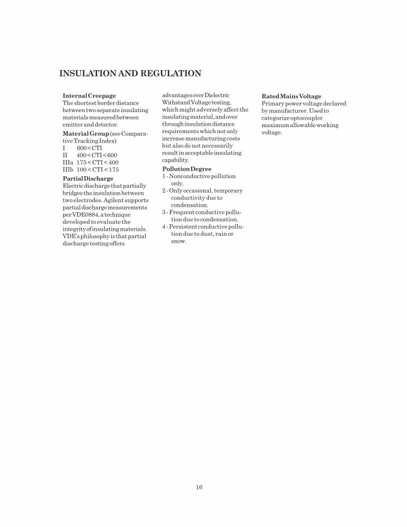
Internal Creepage
The shortest border distance
between two separate insulating
materials measured between
emitter and detector.
Material Group (see Compara-
tive Tracking Index)
I 600 < CTI
II 400 < CTI < 600
IIIa 175 < CTI < 400
IIIb 100 < CTI < 175
Partial Discharge
Electric discharge that partially
bridges the insulation between
two electrodes. Agilent supports
partial discharge measurements
per VDE0884, a technique
developed to evaluate the
integrity of insulating materials.
VDE’s philosophy is that partial
discharge testing offers
advantages over Dielectric
Withstand Voltage testing,
which might adversely affect the
insulating material, and over
through insulation distance
requirements which not only
increase manufacturing costs
but also do not necessarily
result in acceptable insulating
capability.
Pollution Degree
1 - Nonconductive pollution
only.
2 - Only occasional, temporary
conductivity due to
condensation.
3 - Frequent conductive pollu-
tion due to condensation.
4 - Persistent conductive pollu-
tion due to dust, rain or
snow.
Rated Mains Voltage
Primary power voltage declared
by manufacturer. Used to
categorize optocoupler
maximum allowable working
voltage.
INSULATION AND REGULATION
17
Common-Mode Transient Rejection
Circuit designers often encounter
the adverse effects of common-
mode noise in a design. Once a
common-mode problem is
identified, there are several ways
that it can be resolved. However,
common-mode interference
manifests itself in many ways;
therefore, it may be hard to
determine whether it is the cause
of a circuit’s misbehavior. If a
system is connected and running
but only produces erroneous
data, common-mode noise may be
the reason. This section describes
sources of common-mode
problems, presents possible
solutions, and highlights the
technology that Agilent
Technologies' Components Group
uses to produce opto-isolators
with superior Common-Mode
Performance.
Common-mode rejection (CMR)
is a measure of the ability of a
device to tolerate common-mode
proprietary, low-cost Faraday
shield which decouples the
optocoupler input side from the
output side. The second method
is by unique package design
which minimizes input-to-output
capacitance. The importance of
these two strengths is explained
as follows.
Figure 5 illustrates a Common-
mode transient pulse (VCM).
Figure 6a and 6b show interfer-
ence circuit models for two types
of possible common-mode failure
mechanisms for a single-
transistor optocoupler. The
dashed lines are shown to
indicate external components
added to the optocoupler. VCM
represents a voltage spike across
the optocoupler isolation path
between the output-side ground
(VG2) and input-side ground (VG1).
VDM represents a signal voltage
applied across the input side.
noise. Agilent specifies common-
mode rejection as common-
mode transient rejection
(CMTR). CMTR describes the
maximum tolerable rate-of-rise
(or fall) of a common-mode
voltage (given in volts per micro-
second). The specification for
CMTR also includes the amplitude
of the common-mode voltage
(VCM) that can be tolerated.
Common-mode interference that
exceeds the maximum specifica-
tion might result in abnormal
voltage transitions or excessive
noise on the output signal.
(CMTR is slightly different than
common-mode rejection ratio
CMRR, often used for analog
devices and commonly specified
in dB as the ratio of the
differential-mode gain to the
common-mode gain.)
Agilent optocouplers rely on two
key technical strengths to achieve
high CMTR. The first is use of a
Figure 5. Illustration of VCM Common-Mode Pulse.
Figure 6a. Interference CircuitModel.
RL
+ (VCM) –
OPTO-ISOLATOR
COMMON-MODE TRANSIENT
R
V
TRANSMIT SIDE RECEIVE SIDE
VOLTMETER
LEDVDM
VG1INPUT GROUND
VG2OUTPUT GROUND
CSBCIS
iCM
IB
IP
PHOTODIODE
VO
RL
INTERNAL SHIELD
NOTE: iCM GETS DIVERTED TO GROUND, VG2, WHEN INPUT IS OFF.
iCM IS SUPPLIED FROM GROUND, VG2, WHEN OUTPUT IS ON.
VCM
VOLTMETER
INSULATION AND REGULATION

18
COMMON-MODE TRANSIENT REJECTION
Figure 6b. Interference Circuit Model.
LEDVDM
VG1INPUT GROUND
VG2OUTPUT GROUND
CIA
CIC
IBIP
PHOTODIODE
VO
RL
INTERNAL SHIELD
NOTE: CURRENT “STOLEN” FROM LED: iLP = CIA
VCM
dVCMdt
iLP
VOLTMETER
Referring to Figure 6a the para-
sitic distributed capacitance CIS,
which might tend to couple
transient current into the transistor
base node (for example when the
transistor is in the “off” state)
terminates on an internal Faraday
shield. Therefore the transient
current, ICM, gets diverted to
output ground (VG2). Referring to
Figure 6b, the parasitic distrib-
uted capacitances, CIA and CIC are
shown across the LED anode-to-
ground (VG2) and LED cathode-
to-ground (VG2) respectively.
Because the LED anode is at a
relatively higher impedance than
the cathode (i.e., RLED to ground)
current at this point will tend to
be modulated slightly during CM
transients. For instance, if the
LED is on, then during a positive
transient (i.e., dVCM/dt > 0)
current will be diverted away
from the LED. For fast enough
transients, this may turn the LED
off. (If RLED is connected to the
LED cathode side then CIC
provides a parasitic path to divert
current towards or away from the
LED.) This type of failure is
avoided by ensuring that CIA and
CIC are small.
Figure 7 shows the possible
effect on the output voltage level
of an optocoupler due to a
common-mode pulse. The output
is shown (successively) in the
high and low states. (This might
be observed if Rled were con-
nected as in Figures 6a, 6b.)
VCM
VOH
VOL
tTRANSIENT tTRANSIENT
t
VIHVIL
VO
TRANSIENT RATE OF CHANGE =VCM
tTRANSIENT
TRANSIENT AMPLITUDE = VCM
t
Figure 7. Common Mode Interference Effect.

19
Figure 8. Full-Bridge Power Switch Configuration.
ISOLATION
CONTROLCIRCUITRY
GATEDRIVE
GATEDRIVE
GATEDRIVE
ISOLATION
A1 B1
A2B2
MOTOR
HV +
GATEDRIVE
HV -
1 2
transistors (A1, B1) is attached to
the drain of a second set of
transistors (A2, B2). When
transistor set A turns on, set B
turns off. Current flows from the
positive supply, through
transistor A1, through the load,
and through transistor A2. When
set B turns on, set A turns off,
and the polarity of the current
through the inductive load is
reversed.
How does this operation create a
common-mode problem? The
input of each gate drive circuitry
is referenced to the ground of the
digital control circuitry; the
output common, on the other
hand, is floating and referenced
to the source of its associated
power transistor. The floating
commons of the upper gate drive
circuits rapidly switch between
the positive and negative power
supplies. This rapid switching
creates a large voltage swing
across the input to output of the
gate drive circuitry. As an
As long as the amplitude VCM and
value of dVCM/dt are less than the
ratings for the optocoupler being
used, VOH will remain above 2 V
(maximum TTL VIH) and VOL will
remain below 0.8 V (minimum
TTL VIL). Note that the slight
perturbations in output voltage
occur sometime after the input
pulse which causes them, due to
the non-zero response time of the
output transistor to the
“perturbation signal.”
Common-mode signals can
originate from several different
sources. A full bridge power
inverter, shown in Figure 8, is a
good example of an application
that can exhibit large amounts of
common-mode noise. Full-bridge
inverters are commonly found in
motor-speed control and switching
power supply applications. The
power inverter is generally used
to produce an ac output from a
dc input. In a full-bridge inverter
application like that shown in
Figure 8, the source of one set of
example, a half bridge circuit that
switches between +250 V and
-250 V in 100 ns creates a
common-mode transient signal of
5000 V/µs with an amplitude of
500 V (see Figure 9). The device
that carries the control infor-
mation to each MOSFET must be
able to withstand this level of
common-mode interference.
Although this example may seem
extreme, it is a fact that engineers
continue to use faster-switching
transistors to increase motor
efficiency. Power MOSFETs, for
example, are commonly used in
power inverter applications
because they are capable of high
frequency, high power switching.
The fast switching speeds of the
transistors, however, can
generate common-mode signals
with very high rates of change
(dVCM/dt).
The common-mode signal rate of
rise can also be affected by the
reverse recovery characteristics
of diodes D1 and D2 in the power
COMMON-MODE TRANSIENT REJECTION

20
MOTOR
+250 V
Q1
D1
-250 V
+250 V
∆∆∆∆V∆∆∆∆t
500 V0.1 µµµµs
5000 Vµµµµs
= =
V = 500 VCM
dV dt
Vµµµµs = 5000CM
-250 V
100 ns
V CM
Q2
D2
V CM
Figure 9. Half-Bridge Example.
V CM
V CM
I D2
I D2
I Q1
Figure 10. Half-Bridge InverterWaveforms.
mode problems, providing
protection against common-mode
transients with slew rates as fast
as 15 kV/µs at VCM as high as
1500 V.
High electrical noise levels can
also contribute to common-mode
problems. A significant amount of
electrical noise is found in
industrial environments as a
result of the starting and operating
of electric motors. When a large
motor first turns on, it normally
requires a large in-rush current to
reach operating speed. This large
current spike can generate a
significant amount of electrical
noise in its own and nearby
systems. Even the electric motors
in a typical household environ-
ment vary in size from fractional
to low integral horsepower units
and are often noisy ac-operated
or brushed dc-motors. Other
sources of electrical noise include
microwave ovens, welding
equipment, and automobile
ignitions.
Common-mode noise can enter a
system through conductive,
inductive, or capacitive coupling.
An example of a “conducted”
tion. The voltage and current
waveforms shown in Figure 10
illustrate what happens when Q1
turns back on. As Q1 starts to
turn on, the current through D2
begins to decrease. The current
through D2 continues to decrease
and actually goes negative for a
short time due to the storage of
minority carrier charge in its
junction. It is when this charge
has been depleted that D2 begins
to turn off and VCM begins to
increase. If D2 turns off very
quickly, VCM can also rise very
quickly, generating a large
common-mode transient signal.
For the particular case of driving
the gate of an IGBT or power
MOSFET in a power inverter, the
HCPL-3120 IGBT/MOSFET gate
drive optical isolator is an
effective solution for common-
inverter shown in Figure 9; these
diodes are often referred to as
“freewheeling” diodes. If the
inverter is driving an inductive
load, such as a motor winding,
these diodes may become forward
biased during the normal
operation of the inverter. For
example, assume that Q1 of
Figure 9 is turned on, Q2 is off,
and current is flowing through Q1
and into the inductive load. When
Q1 turns off, voltage VCM swings
in the negative direction until
diode D2 becomes forward biased
and conducts the load current.
It is when Q1 turns back on that
very high rates of rise can be
generated. In extreme cases,
when Q1 turns on again, the rate
of rise of voltage VCM is deter-
mined by how quickly diode D2
recovers from forward conduc-
COMMON-MODE TRANSIENT REJECTION

21
Figure 11. AC Equivalent Circuit for HCPL-261X.
noise voltage is the difference in
ground potential that may exist
between two connected systems
in a plant. The two systems may
experience a small voltage
difference between their ground
references. This voltage difference
might cause a ground-loop
current to flow. If the impedance
of the path through which the
ground-loop current flows is large
enough, a significant amount of
interference will result. Capaci-
tive or inductive coupling may
occur when signal wires run close
to ac power cables. Electromag-
netically induced interference
(EMI) can also be coupled from
adjacent signal lines or nearby
equipment, especially in factory
environments. Other sources of
common-mode noise that can be
coupled into a system include
lightning strikes and electrostatic
discharge (ESD).
Optical isolation is a useful tech-
nique for reducing common-mode
interference. Optocouplers, like
transformers and capacitively-
coupled devices, provide isolation
between the input and output of a
system. Transformers, by virtue
of their high primary-to-
secondary capacitance, tend to
have lower CMTR capability.
Capacitively-coupled devices tend
to have poor CMTR capability
(since in these devices fast,
transient common-mode pulses
pass across the coupling capaci-
tor and are not filtered out.)
Optocouplers, having low input-
to-output capacitance, typically
provide better common-mode
rejection than transformers or
capacitively-coupled devices. The
CMR specification of an
optocoupler ranges up to
VCM = 1500 V amplitude and up
to 15,000 V/µs rate of change of
VCM, for high-CMR products.
Another advantage of optocoup-
lers lies in the area of EMI
generation and susceptibility.
Transformers typically radiate
electromagnetic interference
(EMI) and are susceptible to
magnetic fields. Capacitively-
coupled devices generate ground-
loop current, thus generating
EMI. Optocouplers use light for
data transmission; additionally,
they effectively eliminate ground-
loop current. Therefore, they do
not radiate nor are they affected
by stray magnetic fields. This
ability is well-recognized in the
European Community where
systems designers need to
achieve system-level standards
(now adopted as EN50081/
EN50082 which set limits on the
amount of acceptable EMI a
system radiates or to which it is
immune.)
A technique which may be used
to further enhance CMTR is an
“LED split-resistor” technique as
shown in Figure 11; (note that
the VDM which would appear
between the top and bottom
RLEDs has not been shown in this
“ac equivalent circuit”). By using
two LED-resistors (instead of
one) the current change at the
anode of the LED is nearly
canceled by the current change at
the cathode, thus tending to keep
the LED current constant. This
makes the optical isolator more
immune to CM transients where
CLA and CLC limit CMTR.
8
5
1
4
VCC+
15 pFCIC
SHIELD
+ –VCM
63
721/2 RLED
1/2 RLEDiLN
iLP
CIAVO
GND
350 Ω0.01 µF
COMMON-MODE TRANSIENT REJECTION

22
LED Degradation over Time
One concern for optocoupler
lifetime is that LED light-output
(LOP) decreases over time.
Generally, light-output degrada-
tion gets worse with increasing
operating temperature and
operating LED current. A worst-
case scenario is that over time, as
the LED becomes dimmer, the
LOP will fall below the minimum
value needed for a part to switch
properly. Agilent Technologies,
an industry leader in LED
technology, tests LOP
degradation under accelerated
conditions in order to provide
designers with information on the
expected operating lifetime of
optocouplers. Optocouplers
which have an input driver IC are
designed such that the driver IC
sets the proper input IF, guard-
banding for expected LED LOP
degradation over the life of the
optocoupler. (Examples are the
HCPL-3700, HCPL-7101, and
HCPL-7840.) On the other hand,
optocouplers requiring an input
current-setting resistor (i.e.,
without an input driver IC)
require that the circuit designer
guardband the minimum
recommended operating IF by an
amount sufficient to account for
expected LOP degradation.
Agilent has undertaken testing of
LED degradation for periods of
continuous operation up to at
least 10 khours for various LEDs
used in Agilent optocouplers.
Figures 12a and 12b show the
normalized light output over a
10,000 hour period for Gallium
Arsenide Phosphide (GaAsP) and
Aluminum Gallium Arsenide
(AlGaAs) LEDs respectively.
Figure 13 shows LOP as a
function of IF for a GaAsP LED
under operating conditions of
IF = 20 mA at an ambient
temperature of TA = 125°C. Curves
are shown for t = 0 hours and
t = 10 khours of continuous
operation.
Optocouplers which use the
GaAsP and AlGaAs LEDs are
listed in Figures 12a and 12b.
Figure 14 illustrates how, based
on knowledge of initial and post-
stress LOP vs. IF, (for a GaAsP
LED) a minimum guardbanded IF
can be determined to provide for
LOP degradation over the life of
the LED. For this case, the
minimum recommended IF at
t = 0 hours (IF(min)) of 5 mA is
guardbanded for 10 khours of
operation to a value of 6.1 mA.
Note that in Figure 14 if the LOP
vs. IF curves were linear over the
range between IF(min) and IGB(min)
(minimum IF guardbanded for
t = 10 khours) then the amount of
guardbanding (percent change)
would be equal to the amount of
LOP degradation (percent
change). Since in our case the
curve is “concave up” the amountof guardbanding is slightly less
than the percent change in LOP
between t = 0 and t = 10 khours.
Figure 15 (which is a plot of the
slope of the (t = 0) curve in
Figure 14), shows that the slope
is increasing up to about
IF = 20CmA, at which point it
LED DEGRADATION

23
Figure 13. Typical GaAsP LED Light-Output (LOP) vs. IF After 0 khours and 10khours of Continuous Operation at 125°C, IF = 20 mA.
NO
RM
AL
IZE
D T
O L
OP
@ 2
0 m
A
0.1 100.0
1.0
0
IF (mA)
1.0 10.0
0.1
0
LOP (NORMALIZED)BEFORE STRESS
ESTIMATED LOP(NORMALIZED)AFTER 10 kHOURSBASED ON %DEGRADATIONAFTER STRESS OF IF = 20 mA(ACTUAL PERCENTDEGRADATIONWILL BE SMALLERWITH IF < 25 mA)
flattens out and begins
decreasing.
By empirically modeling the
typical GaAsP LOP vs. IF curve
and applying knowledge of worst-
case (-3 σ) degradation over time,
guardbanded IGB(min) for a typical
LED can be reduced to the
following equation:
IF(min) IGB(min) = ––––––
1–a
δ
≈ IF(min) × 1.214
where,
IF(min) = minimum recommended
IF at t = 0 hours.
IGB(min) = minmum guardbanded
IF after t = 10 khours.
a = 1.3 (empirical curve - fit)
δ = Post-stress LOP Factor
(≈ 0.784 for 10 khours,
TA = 125°C, IF = 20 mA)
This equation applies well when
IF is approximately constant.
Example: To calculate the
appropriate IGB(min) for an
HCPL-3120 note that
IF(min) = 7 mA. Applying the
above relationship for 10 khour
guardbanding,
IGB(min) = 8.50 mA.
LED DEGRADATION
NO
RM
AL
IZE
D L
ED
LIG
HT
OU
TP
UT
AT
t =
0 h
r
0 10
1.2
0.5
TIME (kHOURS)
1.1
0.7
1 7
MEAN LOP
MEAN - 3 σ LOP
1.0
0.9
0.8
0.6
2 3 4 5 6 8 9
GaAsP LEDS ARE USED IN:6N135/6/7/8/94N45/66N134, 6N140HCPL-4502/3/4/6HCPL-02XX, HCPL-22XXHCPL-05XX, -25XX, -06XX, -26XX, -07XX, -27XXHCPL-4100, -4200, -370X, -3120, -3150HCPL-55XX, -65XX, -56XX, -66XX, -57XX, -67XX
MEASURED IF = 16 mASTRESSED IF = 20 mA
Figure 12a. Normalized LED Light Output (LOP) vs. Time for GaAsP LED(Stress IF = 20 mA, TA = 125°C).
NO
RM
AL
IZE
D L
ED
LIG
HT
OU
TP
UT
AT
t =
0 h
r
0 10
1.2
0.5
TIME (kHOURS)
1.1
0.7
1 7
1.0
0.9
0.8
0.6
2 3 4 5 6 8 9
AlGaAs (TYPE 1) LED IS USED IN:HCNW22XX/26XX/45XX/4562HCNW135/6/7/8/9HCNR200/1HCPL-78XXHCPL-7100/1HCPL-7601/11
MEAN LOP
MEAN - 3 σ LOP
MEASURED IF = 5 mASTRESSED IF = 25 mA
Figure 12b. Normalized LED Light Output (LOP) vs. Time for AlGaAs LED(Stress IF = 25 mA, TA = 125°C).
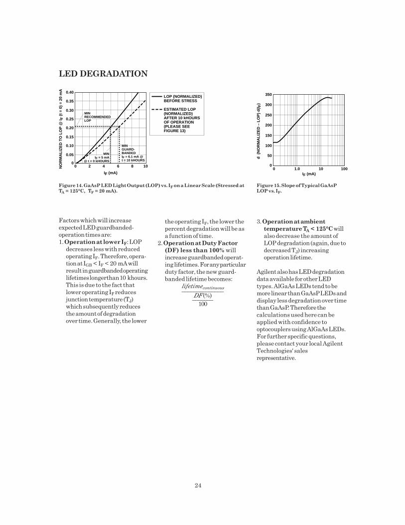
24
Figure 15. Slope of Typical GaAsPLOP vs. IF.
Figure 14. GaAsP LED Light Output (LOP) vs. IF on a Linear Scale (Stressed atTA = 125°C, TF = 20 mA).
d (
NO
RM
AL
IZE
D –
LO
P)
d(I
F)
0 100
350
0
IF (mA)
250
150
1.0 10
100
200
300
50
Factors which will increase
expected LED guardbanded-
operation times are:
1. Operation at lower IF: LOP
decreases less with reduced
operating IF. Therefore, opera-
tion at IGB < IF < 20 mA will
result in guardbanded operating
lifetimes longer than 10 khours.
This is due to the fact that
lower operating IF reduces
junction temperature (TJ)
which subsequently reduces
the amount of degradation
over time. Generally, the lower
3. Operation at ambient
temperature TA < 125°C will
also decrease the amount of
LOP degradation (again, due to
decreased TJ) increasing
operation lifetime.
Agilent also has LED degradation
data available for other LED
types. AlGaAs LEDs tend to be
more linear than GaAsP LEDs and
display less degradation over time
than GaAsP. Therefore the
calculations used here can be
applied with confidence to
optocouplers using AlGaAs LEDs.
For further specific questions,
please contact your local Agilent
Technologies' sales
representative.
the operating IF, the lower the
percent degradation will be as
a function of time.
2. Operation at Duty Factor
(DF) less than 100% will
increase guardbanded operat-
ing lifetimes. For any particular
duty factor, the new guard-
banded lifetime becomes:
lifetimecontinuous––––––––––––––
DF (%)–––––––
100
NO
RM
AL
IZE
D T
O L
OP
@ I F
(t
= 0)
= 2
0 m
A
0 10
0.40
0
IF (mA)
4 6
0.25
0.15
LOP (NORMALIZED)BEFORE STRESS
ESTIMATED LOP(NORMALIZED)AFTER 10 kHOURSOF OPERATION(PLEASE SEEFIGURE 13)
2 8
0.35
0.30
0.20
0.10
0.05
MINRECOMMENDEDLOP
MINIF = 5 mA
@ t = 0 kHOURS
MINGUARD-BANDEDIF = 6.1 mA @t = 10 kHOURS
LED DEGRADATION

25
ESD Precautions: Standard
electrostatic discharge precau-
tions should be taken in handling
and assembly of the optocouplers
to prevent damage or degradation
of the device.
Printed Circuit Board Layout:
An optocoupler performs reliably
only in a correctly designed
circuit. In most digital optocoup-
lers the amplifier at the output is
required to operate with the very
low photocurrent from the
photodetector. Consequently
these amplifiers can be sensitive
to electrical disturbances. It is
therefore necessary to have
proper shielding and bypassing of
the VCC and Ground traces.
Bypassing closely to each of the
optocouplers VCC-to-Ground pins
with low-inductance ceramic
capacitor is recommended as
shown in Figure 17.
Figure 17 shows an optional PCB
layout for a high speed digital
optocoupler for improving
electrical noise immunity. The
optional VCC and Ground traces
between the pin rows of the
optocoupler help shield the
output circuitry from electrical
disturbances on the input pins,
thus improving common-mode
rejection.
Guidelines for Printed Circuit Board Assemblyand Layout
Agilent optocouplers are suitable
for automatic printed circuitboard (PCB) assembly operations
including surface mount assembly.
The following guidelines are
recommended for proper opera-
tion and long term reliability of
Agilent optocouplers.
Solder Reflow Process: Only one
soldering operation is recom-
mended within the thermal
profile shown in Figure 16. With
infrared lamp heating, use
precautions to avoid localized
temperature rise in the resin.
Also, the resin should not be
Figure 16. Temperature/Time Thermal Profile.
250
200
100
180°C
2.5°C±0.5°C/sec.
3°C+1°C/-0.5°C
Peak Temperature245°C Peak Temperature
240°C
Peak Temperature230°C
Soldering Time200°C
200°C
30 sec
Pre Heating Rate: 3°C+1°C/-0.5°C/sec.Reflow Heating Rate: 2.5°C±0.5°C/sec.
150°C140°C
RoomTemperature
00 50 100 150 200 250
TEM
PER
ATU
RE
(°C
)
TIME (seconds)
30 sec
50 sec
TIGHTTYPICALLOOSE
Pre Heating Time150°C, 90±30 sec.
immersed in the solder. To
prevent chloride corrosion of the
lead frame, halide fluxes should
not be used.
Wave Soldering: The maximum
solder temperature allowed is
260°C for 10 seconds, with the
solder 1.6 mm below the seating
plane.
Solvent Cleaning: The solvent
temperature and immersion time
should not exceed 45°C and three
minutes respectively. For ultra-
sonic cleaning, environmentally
safe solvents such as ethyl and
methyl alcohol are recommended.
Figure 17. Optional Printed Circuit Board Layout for Improved Electrical Noise Immunity.
GND BUS
V BUSCC
OUTPUT
10 mm MAX
0.1µF
HCPL-2601/11 HCPL-2601/11
VCC1
2
3
4
8
7
6
5
VE
VOUT
GND
ANODE
CATHODE
LED DEGRADATION

Digital Optoisolators:An Overview
Introduction
Agilent Technologies offers a wide
array of Optoisolators for noise
rejection, ground loop current
elimination, and high voltage
isolation for digital data
transmission and communication
applications. The product offering
includes low speed (100 kbit/s to
1CM bit/s) split Darlington or
single transistor type
optoisolators to high speed 25 M
bit/s cascaded amplifier stage
optoisolators with Schottky
transistor or CMOS output stage.
DescriptionFigure 1 shows a Photodiode/
Transistor Optoisolator where a
PIN photodiode detector is coupled
to a single transistor amplifier
output stage (e.g. HCPL-4504).
Compared to a typical
phototransistor optoisolator, a PIN
photodetector diode reduces the
base-collector “Miller” capacitance
and allows operability at a much
higher speed.
Figure 2 shows a Split Darlington
Output Stage, where an emitter-
follower stage is added between a
PIN photodiode and the output
amplifier. This allows the
optoisolator to be driven at a
much lower input drive current,
as low as 40 mA for the HCPL-
4701/HCPL-4731 family or
0.5CmA for the 6N139 family. This
allows much higher current
transfer ratio (CTR) or current
gain at the output, and TTL/
CMOS gates can be easily driven.
Figure 1. Photodiode/Transistor Optoisolator
Figure 2. Split Darlington Transistor Optoisolator
1
1
2
8
7
6
5
LED
V+
3
4SHIELD
HCPL-4504HCPL-0454HCNW4504
PHOTODIODE(PIN)
2
RINRL
VOUT
IF
TRANSISTORAMPLIFIER
VIN
1
1
2
8
7
6
5
LED
3
4SHIELD
HCPL-07016N139/8
HCPL-4701/4731
PHOTODIODE(PIN)
2
R1RL
VOUT
VCC
IF
SPLITDARLINGTON
AMPLIFIER
VIN
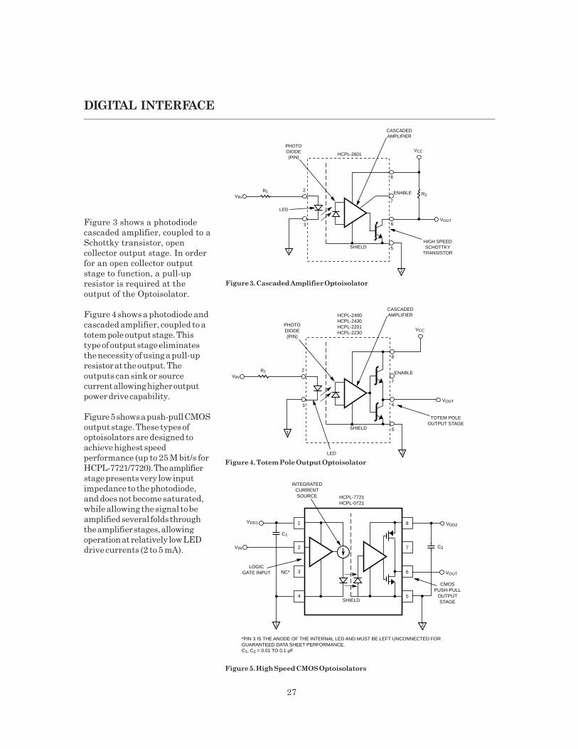
27
Figure 3 shows a photodiode
cascaded amplifier, coupled to a
Schottky transistor, open
collector output stage. In order
for an open collector output
stage to function, a pull-up
resistor is required at the
output of the Optoisolator.
Figure 4 shows a photodiode and
cascaded amplifier, coupled to a
totem pole output stage. This
type of output stage eliminates
the necessity of using a pull-up
resistor at the output. The
outputs can sink or source
current allowing higher output
power drive capability.
Figure 5 shows a push-pull CMOS
output stage. These types of
optoisolators are designed to
achieve highest speed
performance (up to 25 M bit/s for
HCPL-7721/7720). The amplifier
stage presents very low input
impedance to the photodiode,
and does not become saturated,
while allowing the signal to be
amplified several folds through
the amplifier stages, allowing
operation at relatively low LED
drive currents (2 to 5 mA).
Figure 3. Cascaded Amplifier Optoisolator
Figure 4. Totem Pole Output Optoisolator
Figure 5. High Speed CMOS Optoisolators
1
2
8
7
6
5
LED
3
SHIELD
HCPL-2400HCPL-2430HCPL-2201HCPL-2230
PHOTODIODE(PIN)
2
R1
VOUT
VCC
TOTEM POLEOUTPUT STAGE
VINENABLE
CASCADEDAMPLIFIER
1
2
8
7
6
5
LED
3
SHIELD
HCPL-2601
PHOTODIODE(PIN)
2
R1 R2
VOUT
VCC
HIGH SPEEDSCHOTTKY
TRANSISTOR
VINENABLE
CASCADEDAMPLIFIER
1
1
2
8
7
6
5
LOGICGATE INPUT 3
4SHIELD
HCPL-7721HCPL-0721
INTEGRATEDCURRENTSOURCE
2
C2
VOUT
VDD2
CMOSPUSH-PULL
OUTPUTSTAGE
VIN
VDD1
C1
NC*
*PIN 3 IS THE ANODE OF THE INTERNAL LED AND MUST BE LEFT UNCONNECTED FORGUARANTEED DATA SHEET PERFORMANCE.C1, C2 = 0.01 TO 0.1 µF
DIGITAL INTERFACE

Digital Logic Interface/LevelShifting Applications
Description
The circuit shown is an interface
between two TTL gates using an
active output (totem pole) opto-
coupler, the HCPL-2201. A series
switching circuit drives the
optocoupler LED. The designer
chooses RIN to agree with the
equation shown in the schematic.
The active output of the HCPL-
2201 can be directly connected to
a TTL gate, and no pull-up
resistor is required. The HCPL-
2201 can sink enough current to
handle up to 16 LSTTL or 4 TTL
loads.
Performance of Circuit• Maximum optocoupler propa-
gation delay: 300 ns (refer to
alternative Agilent parts for
lower propagation delay times)
• Typical signaling rate: dc to 5
MBd (refer to alternative
Agilent parts for higher speeds)
• Typical optocoupler LED drive
current: 2 mA
Benefits• No pull-up resistor required on
the optocoupler output
interface
• Low power dissipation on the
optocoupler input circuit
• Up to 20 V supply voltage for
the HCPL-2201
Alternative Agilent Parts
1) HCPL-07XX, HCPL-2730/1,
HCPL-4701, 6N138/9,
CNW138/9 Low Input Current
Optocouplers
2) HCPL-0201/11 Small-Outline
Logic-Gate Optocoupler
3) HCPL-52XX Hermetically
Sealed Logic-Gate
Optocoupler
4) CNN2201/11 Widebody
Logic-Gate Optocoupler
5) HCPL-2230/1 Dual-Channel
Logic-Gate Optocoupler
6) HCPL-05XX, HCPL-2530/1,
HCNW135/6, 6N135/6 High
Speed Optocoupler
7) HCPL-250L/260L/270L,
HCPL-050L/060L/070L
3.3VCOptocouplers
TTL Interface with Series LED Drive
DATAOUTPUT
DATAINPUT
7
5
6
8
2
3
4
1
HCPL-2201
VCC2(+5 V)
VCC2
GND
21
TTL/LSTTL
VCC1(+5 V)
0.1 µF
TTL/LSTTL
RIN
TOTEM POLEOUTPUTGATE
RIN =V - V - VCC1 F OL
IF
RECOMMENDED R = 1.1 kΩIN

29
Description
The above circuit shows how a
0 to 5 V logic signal can be level
shifted to a -15 to 0 V signal. The
circuit can safely be used for level
shifting up to ±800 V. The circuit
uses an open collector output
logic gate, the 74LS405, to drive
the LED of the HCPL-4502/3
optocoupler. The HCPL-4502/3
also has an open-collector output.
The designer chooses RIN to agree
with the equation shown in the
schematic. This equation sets the
value of the optocoupler LED
forward current. The output of
the HCPL-4502/3 requires a pull-
up resistor, RL. The current-
transfer ratio (CTR) of the
optocoupler determines the
maximum amount of current the
optocoupler output can sink while
maintaining the output voltage
(between pins 5 and 6) of 0.5 V or
less.
Performance of Circuit
• Maximum optocoupler
propagation delay: 2 µs (refer to
alternative Agilent parts for
lower propagation delays)
• Typical signaling rate: dc to 1
MBd (refer to alternative
Agilent parts for higher speeds)
• Typical optocoupler LED drive
current: 10 to 16 mA
• Maximum output supply voltage
(pins 8-5): 30 V
• Minimum CMR: 15 kV/µs slew
rate, 1500 V peak
Benefits
• Reduces transient immunity
problems
• Convenient way of replacing
pulse transformer for high-
voltage level shifting
Alternative Agilent Parts
1) HCPL-07XX, HCPL-2730/1,
HCPL-4701, 6N138/9,
HCNW138/9 Low Input
Current Optocouplers
2) HCPL-55XX Hermetically
Sealed High Speed
Optocoupler
3) HCPL-0710 SO-8 High Speed
CMOS Optocoupler
4) HCPL-250L/260L/270L,
HCPL-050L/060L/070L
3.3VCOptocouplers
IF
7
5
6
8
2
3
4
1
NOTE: FOR BEST CMR PERFORMANCE, CONNECT PIN 7 TO PIN 8.
INR
74LS05
INR = 5 - VF
HCPL-4502/3
+5 V
IFLR
OLV
-15 V
IO (min) = IF • CTR (min)
RL (min) = 15 – VOL
IO (min) + IIL
IILIO
VIN
VOUT
DIGITAL INTERFACE:
Level Shifting/TTL Interface with Shunt LED Drive

30
Description
A CMOS-to-CMOS interface is
possible with Agilent opto-
couplers. The above circuit
shows an interface circuit for
8CMBd applications. Over the
temperature range a CMOS
CD4050 Hex Buffer can source
about 0.7 mA (minimum), which
is sufficient to drive the
HCPL-2300/HCPL-0300
optocoupler. The 20 pF capacitor
allows peaking currents to assist
the LED turn on and off quickly.
Performance of Circuit
• Optocoupler LED current:
0.5 mA minimum
• Typical signaling rate: dc to
8 MBd
Benefits
• Low power consumption
• Simple interface
Alternative Agilent Parts
1) HCPL-7721/7720/7710 High
Speed CMOS Optocoupler
2) HCPL-0721//0720/0710 Small
Outline High Speed CMOS
Optocoupler
DIGITAL INTERFACELow Power 8 MBd CMOS Interface
HCPL-2300/HCPL-0300
1 kΩ
CD4050 CD4050
0.1µF
RL
VDD2
VO2
35
6
8
7VIN
VDD1 20 pF
RI
1 2
5 V
VDD1(V)
51015
RI(kΩ)
5.1113.319.6
VDD1(V)
51015
RL(kΩ)
12.373.16

31
DIGITAL INTERFACE
25 MBd CMOS Interface
8
7
6
1
3
SHIELD5
2
4
VDD1
GND1
VDD2
VOUT
IO
LED1
NC
GND2
VIN74HCTO4
74HCTO4
C2C1
HCPL-7721
C1, C2 = 0.01 µF TO 0.1 µF
Description
Up to 25 MBd CMOS-to-CMOS
interface is possible with the
HCPL-7721 optocouplers. The
above circuit requires only a
bypass capacitor on each of the
HCPL-7721 input-side and output-
side power supply pins.
Performance of Circuit
• Typical logic low input power
supply current for HCPL-7721:
1.5 mA
• Typical logic low input power
supply current for HCPL-7721:
7 mA
• Typical HCPL-7721 signalling
rate: dc to 25 MBd
• Typical HCPL-7721 pulse-width
distortion: 3 ns
• Typical HCPL-7721 propagation
delay: 20 ns
Benefits
• Lower power consumption
• Very simple interface
Alternative Agilent Parts1) HCPL-0721: SO8 package
2) HCPL-7720/0720: 25 MBd,
8 ns PWD CMOS interface
optocoupler
3) HCPL-7710/0710: 25 MBd,
8 ns PWD CMOS interface
optocoupler
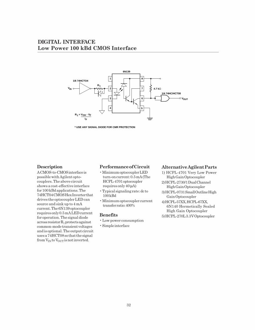
32
VOUT
IF
7
5
6
8
2
3
4
1
* USE ANY SIGNAL DIODE FOR CMR PROTECTION
INV1R
1/6 74HCTO4
1R = V - VOH F
4.7 kΩ* 1/4 74HC/HCT08
6N139
Performance of Circuit
• Minimum optocoupler LED
turn-on current: 0.5 mA (The
HCPL-4701 optocoupler
requires only 40 µA)
• Typical signaling rate: dc to
100 kBd
• Minimum optocoupler current
transfer ratio: 400%
Benefits• Low power consumption
• Simple interface
Alternative Agilent Parts1) HCPL-4701 Very Low Power
High Gain Optocoupler
2) HCPL-2730/1 Dual Channel
High Gain Optocoupler
3) HCPL-0731 Small Outline High
Gain Optocoupler
4) HCPL-57XX, HCPL-67XX,
6N140 Hermetically Sealed
High Gain Optocoupler
5) HCPL-270L 3.3V Optocoupler
DIGITAL INTERFACE
Low Power 100 kBd CMOS Interface
Description
A CMOS-to-CMOS interface is
possible with Agilent opto-
couplers. The above circuit
shows a cost-effective interface
for 100 kBd applications. The
74HCT04 CMOS Hex Inverter that
drives the optocoupler LED can
source and sink up to 4 mA
current. The 6N139 optocoupler
requires only 0.5 mA LED current
for operation. The signal diode
across resistor R1 protects against
common-mode transient voltages
and is optional. The output circuit
uses a 74HCT08 so that the signal
from VIN to VOUT is not inverted.

33
VOUT
VIN
HCPL-4701
2
RL
100 Ω VCC2 = 3 V
2 2
0.1 µF
R174LVU04
*
* USE ANY SIGNAL DIODE
1
1
VCC1 = 3 V
TYPICAL POWER DISSIPATION FOR 3 V APPLICATION(VCC1 , VCC2 = 3.0 V, RL = 11 kΩ, R1 = 43.8 kΩ)
VCC1 SIDE:
OPTOCOUPLER LED
INPUT RESISTOR R1TOTAL VCC1 SIDE
50 µW
70 µW
120 µW
VCC2 SIDE:
OPTOCOUPLER (VO , VCC2)
PULL-UP RESISTOR RLTOTAL VCC2 SIDE
85 µW
790 µW
875 µW
RECOMMENDED VCC FILTER
10.0 µF
Description
The HCPL-4701 low-power
optocoupler is used for 3 V-to-3 V
Logic interface across an
isolation barrier. Only 40 µA of
LED current (IF) is required to
turn-on the optocoupler. Typical
power for dissipation for just the
optocoupler is 135 µW at IF =
40 µA, and 965 µA at IF = 500 µA.
Performance ofOptocoupler• Typical optocoupler current
transfer ratio: 3500% at
IF = 40 µA
• Input current for optocoupler
turn-on: 40 µA
Benefits• Low power dissipation
DIGITAL INTERFACEIsolated 3 V Logic Interface/Battery Operated Applications
Alternative Agilent Parts1) HCPL-4731 Dual Low Power
Optocoupler
2) HCPL-070A SO-8 Low Power
Optocoupler
3) HCPL-073A SO-8 Dual Channel
Low Power Optocoupler
4) HCPL-050L/060L/070L,
HCPL-250L/260L/270L
3.3VCOptocouplers

Description
The above schematic shows a
very simple RS-232C data
communication isolation
interface using a 6N139
optocoupler. This circuit operates
with an LED forward current of
0.5 mA when the input is at 3 V.
The 1N4150 diode protects the
LED during negative signal
voltages. Since a low diode
current is used to operate the
6N139, the twisted pair line can
be up to 120 m. However, the data
rate may have to be lowered to
account for slower charging and
discharging of the total line
capacitance.
Performance of Circuit
• RS-232C link twisted pair cable
length: up to 120 m for low data
rates
• Typical optocoupler propaga-
tion delay: 20 µs
Benefits
• Simple, low cost isolated
interface
• Meets worldwide regulatory
standards for isolation
Alternative Agilent Parts
1) HCPL4701, 6N138/9, 4N45/6,
HCPL-2730/1 High-Gain, Low
Input Current Optocoupler
2) HCPL-0700/1, HCPL-0730/1,
HCPL-M700/1 Small Outline
High-Gain, Low Input Current
Optocoupler
3) HCPL-270L/HCPL-070L 3.3V,
100 kBd Optocoupler
Data CommunicationsApplications
VO
7
5
6
8
2
3
4
1
RS-232CINPUT
(± 3 V TO ± 25 V)
3.3 kΩ
CMOS or LSTTL
6N139
CCV
LR
1N4150
Isolated RS-232C/E Interface

35
DescriptionThe above isolated RS-232 circuit
uses two high-speed 3.3V
optocouplers that can switch up
to 15 MBd signals. An isolated
power supply is required to
power the DS14C335 driver/
receiver integrated circuit.
Performance of Circuit• Typical signaling rate: up to
15CMBd
• Optocoupler LED drive current:
5 mA
• Typical Optocoupler Transient
Rejection: 10,000 V/µs slew
rate, 50 V peak
Benefits• Compact design with small
outline optocouplers
• Prevents common-mode
transients from interfering with
the signal
• Low power dissipation
Alternative Agilent Parts1) HCPL-263L/HCPL-063L Dual
Low Power Optocoupler
2) HCPL-250L or HCPL-270L for
low data rate applications
DATA COMMUNICATIONSIsolated 3.3V RS-232 Interface
R1
HCPL-260L
DIGITALLOGIC
R2
21
RS232OUTPUT
R3
HCPL-260L
R4
21
RS232INPUT
3.3V
3.3V
DS14C335
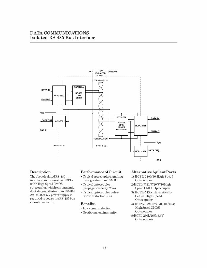
36
Performance of Circuit
• Typical optocoupler signaling
rate: greater than 10 MBd
• Typical optocoupler
propagation delay: 28 ns
• Typical optocoupler pulse-
width distortion: 2 ns
Benefits• Low signal distortion
• Good transient immunity
Alternative Agilent Parts
1) HCPL-2400/30 High Speed
Optocoupler
2) HCPL-7721/7720/7710 High
Speed CMOS Optocoupler
3) HCPL-54XX Hermetically
Sealed High Speed
Optocoupler
4) HCPL-0721/0720/0710 SO-8
High Speed CMOS
Optocoupler
5) HCPL-260L/263L 3.3V
Optocouplers
Description
The above isolated RS-485
interface circuit uses the HCPL-
26XX High Speed CMOS
optocoupler, which can transmit
digital signals faster than 10 MBd.
An isolated 5 V power supply is
required to power the RS-485 bus
side of the circuit.
DATA COMMUNICATIONSIsolated RS-485 Bus Interface
RS-485LINE
DR/RX
RS-485LINE
DRIVERRECEIVER
HCPL-2631
TERMINATION
DATA IN
ENABLE
DATA OUTDATA IN
ENABLE
VCC
DATA OUT
GND
VCC
GND 1
ISOLATION
TERMINATION
DS75176A
DS75176A
+5 VISOLATEDSUPPLY
+5 V COMMON
HCPL-2631
HCPL-2601
HCPL-2601
RS-485 BUS
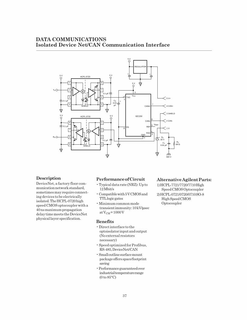
37
DescriptionDeviceNet, a factory floor com-
munication network standard,
sometimes may require connect-
ing devices to be electrically
isolated. The HCPL-0720 high
speed CMOS optocoupler with a
40 ns maximum propagation
delay time meets the DeviceNet
physical layer specification.
Performance of Circuit
• Typical data rate (NRZ): Up to
12 Mbit/s
• Compatible with 5 V CMOS and
TTL logic gates
• Minimum common mode
transient immunity: 10 kV/µsec
at VCM = 1000 V
Benefits• Direct interface to the
optoisolator input and output
(No external resistors
necessary)
• Speed optimized for Profibus,
RS-485, DeviceNet/CAN
• Small outline surface mount
package offers space/footprint
saving
• Performance guaranteed over
industrial temperature range
(0 to 85°C)
Alternative Agilent Parts:1) HCPL-7721/7720/7710 High
Speed CMOS Optocoupler
2) HCPL-0721/0720/0710 SO-8
High Speed CMOS
Optocoupler
DATA COMMUNICATIONSIsolated Device Net/CAN Communication Interface
8
5 V
7
1
2
2
3
4
6
5SHIELD
HCPL-0720
RX
1
1
5 V
2
2
8
7
6
5
3
4SHIELD
HCPL-0720
0.1 µF
5 V
5 V
5 V
TX
R11M Ω
D130 V
REGULATOR
C10.01 µF
7
VREF
82C250
3
6
5
4
CANH
TXD
1 V-
3 SHIELD
2 CAN-
4 CAN+
5 V+
RS
CANL
REF
RXD
500 V
2
C40.01µF
GND
VCC
1+
8
2
0.1 µF
5 V
0.1 µF
0.1 µF
1
2
+ +
2
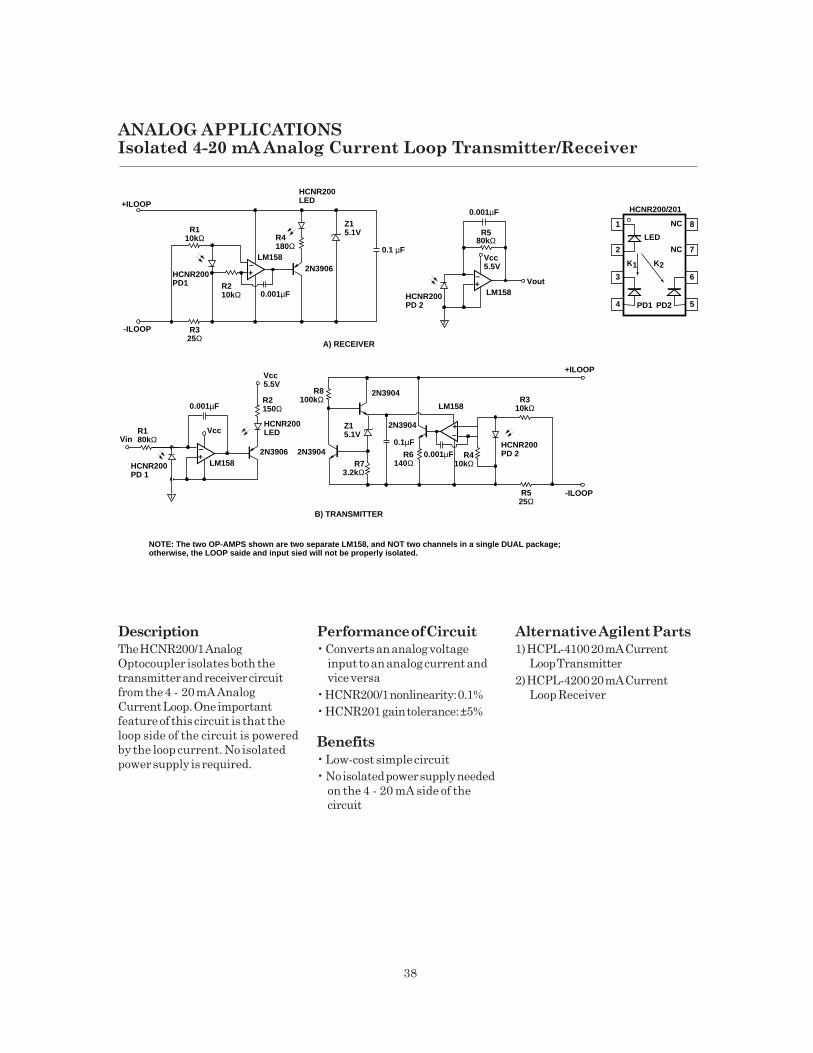
38
ANALOG APPLICATIONSIsolated 4-20 mA Analog Current Loop Transmitter/Receiver
DescriptionThe HCNR200/1 Analog
Optocoupler isolates both the
transmitter and receiver circuit
from the 4 - 20 mA Analog
Current Loop. One important
feature of this circuit is that the
loop side of the circuit is powered
by the loop current. No isolated
power supply is required.
Performance of Circuit• Converts an analog voltage
input to an analog current and
vice versa
• HCNR200/1 nonlinearity: 0.1%
• HCNR201 gain tolerance: ±5%
Benefits
• Low-cost simple circuit
• No isolated power supply needed
on the 4 - 20 mA side of the
circuit
Alternative Agilent Parts1) HCPL-4100 20 mA Current
Loop Transmitter
2) HCPL-4200 20 mA Current
Loop Receiver
A) RECEIVER
B) TRANSMITTER
8
7
6
1
3
HCNR200/201
5
2
4
LED
NC
NC
PD1 PD2
K1 K2
R325Ω
R110kΩ
R210kΩ
HCNR200PD1
0.001µF
2N3906LM158
Z15.1V
0.1 µF
HCNR200LED
R4180Ω
-ILOOP
+ILOOP
–+
HCNR200PD 2
LM158Vout
Vcc5.5V
–+
2
0.001µF
R580kΩ
R310kΩ
R410kΩ
2N3904
2N3904
2N3906
LM158
2N3904
Z15.1V
HCNR200PD 1
NOTE: The two OP-AMPS shown are two separate LM158, and NOT two channels in a single DUAL package;otherwise, the LOOP saide and input sied will not be properly isolated.
HCNR200LED
R2150Ω
R180kΩ
-ILOOP
+ILOOP
Vin
Vcc5.5V
HCNR200PD 2
R525Ω
R73.2kΩ
R8100kΩ
R6140Ω
–+
0.001µF
0.001µF
0.1µF
LM158
Vcc
–+
1

39
DescriptionThe above half-duplex, point-to-
point, multi-drop, 20 mA current
loop configuration can alternat-
ingly transmit bi-directional data
over two wires. Only one current
source is required. Each isolated
station with an HCPL-4100
transmitter and HCPL-4200
receiver optocouplers provides
excellent common-mode
rejection.
Performance of Circuit
• 1 mA noise margin in the
“space” state
• 8 mA noise margin in the
“mark” state
• Typical signal rate and distance:
40 m at 100 kBd; over 200 m at
10 kBd
Benefits• Maintains data integrity
• Simple data transmission
system for industrial
applications
HCPL-4100 TRANSMITTER HCPL-4100 RECEIVER
DATA COMMUNICATIONSIsolated 20 mA Current Loop Interface
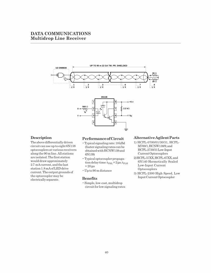
40
Description
The above differentially driven
circuit can use up to eight 6N138
optocouplers at various receivers
along the 90 m line. All stations
are isolated. The first station
would draw approximately
2.7 mA current, and the last
station 1.8 mA of LED drive
current. The output grounds of
the optocoupler may be
electrically separate.
Performance of Circuit• Typical signaling rate: 18 kBd
(faster signaling rates can be
obtained with HCNW139 and
6N139)
• Typical optocoupler propaga-
tion delay time: tPHL = 2 µs; tPLH
= 20 µs
• Up to 90 m distance
Benefits• Simple, low-cost, multidrop
circuit for low signaling rates
Alternative Agilent Parts
1) HCPL-0700/01/30/31, HCPL-
M700/1, HCNW138/9, and
HCPL-2730/31 Low-Input
Current Optocouplers
2) HCPL-57XX, HCPL-67XX, and
6N140 Hermetically Sealed
Low-Input Current
Optocouplers
3) HCPL-2300 High Speed, Low
Input Current Optocoupler
VO
7
5
6
8
2
3
4
1
X
6N138
+5 v
2.2 kΩ
IF
Y
560 Ω
UP TO 90 m 22 GA TW. PR. SHIELDED
1X
1/2 DM8830
Y2XY
3XY
6XY
7XY
8XY
39 Ω
39 Ω
DATA COMMUNICATIONSMultidrop Line Receiver

41
DescriptionA balanced RS-422 line driver
differentially drives a twisted pair
line. Two HCPL-2300s provide
balanced signal direction for this
line. The thresholds of the HCPL-
2300 will be nearly equal, provid-
ing symmetrical signal detection
level. Since the propagation
delays of the two optocouplers
are similar, the pulse-width
distortion for this scheme will be
quite low for considerable line
lengths. The Exclusive-Or flip-
flop circuit at the optocoupler
output increases CMR protection
to an extremely high level and
balances the propagation delays.
For less demanding noise
environments, only one HCPL-
2300 with no EX-OR flip-flop may
be used. The maximum data rate,
however, will be somewhat
lower.
Performance of Circuit
• Signaling rate: > 10 MBd at 100
m line length
• Common mode rejection:
> 15,000 V/µs
Benefits
• Very high common-mode
transient rejection
• Data transmission for up to
1 km distance
Alternative Agilent PartsHCPL-2602/12 High CMR Line
Receiver
DATA COMMUNICATIONSIsolated Balanced Line Receiver - Circuit No. 1
C1*R1
*
TY
PIC
AL
SIG
NA
L R
AT
E –
BA
UD
1
100M
10K
L – LINE LENGTH – METERS
10 1000 10,000
10M
1M
100K
100
BALANCEDSPLIT PHASE
BALANCED(SINGLE
HCPL-2300NO EX- OR FF)
10% PULSE WIDTH DISTORTION22 AWG UNSHIELDED TWISTEDPAIR WIRE CABLE (DEARBORNNO. 862205)
TA = 25 °C
/ HCPL-0300
/ HCPL-0300

42
Description
This is a differential receiver
using a dual-channel HCPL-2630
Optocoupler. The receiver circuit
can handle data up to 10 Mbd for
short line lengths. The capaci-
tance of the twisted-pair wire
introduces a propagation delay
and, as a result, the data rate
decreases with increasing line
length. At the optocoupler output,
an optional Exclusive-Or circuit
can be used to increase CMR and
to balance the propagation
delays.
Performance of Circuit• Signaling rate: up to 10 MBd
• Optocoupler common mode
rejection: 10,000 V/µs
Benefits
• Dual channel optocoupler
reduces boardspace
• Balanced circuit increases CMR
performance thereby eliminat-
ing or reducing transient
interference
Alternative Agilent Parts
1) HCPL-0631 Small Outline,
Dual-Channel, High Speed
Optocoupler
2) HCPL-4661 High-CMR, Dual-
Channel Optocoupler
3) HCPL-56XX Hermetically
Sealed High Speed
Optocouplers
1 2
Z
H H
DATA
L
ICM
RS
VCM
H
L
HCPL-2631
H
L
0.1 µF RL
LSTTL EXCLUSIVE–OR FLIP FLOP
H
L
RL
+5 V
DATA COMMUNICATIONSIsolated Balanced Line Receiver - Circuit No. 2
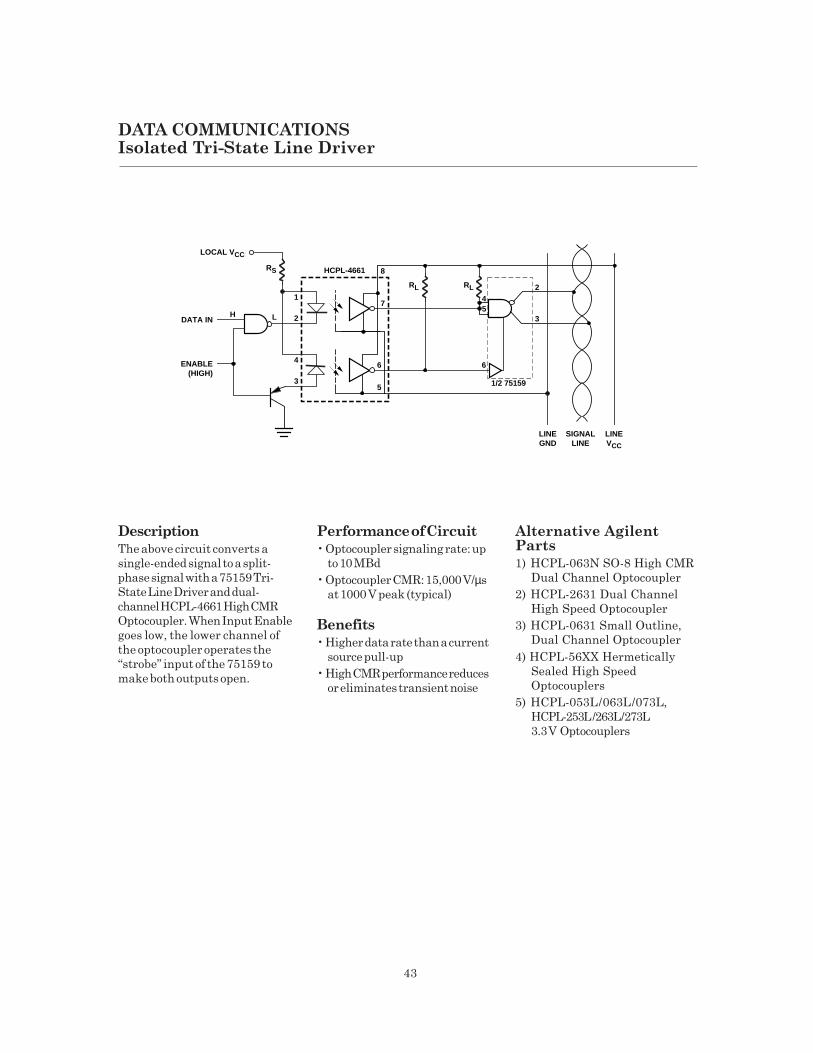
43
Description
The above circuit converts a
single-ended signal to a split-
phase signal with a 75159 Tri-
State Line Driver and dual-
channel HCPL-4661 High CMR
Optocoupler. When Input Enable
goes low, the lower channel of
the optocoupler operates the
“strobe” input of the 75159 to
make both outputs open.
Performance of Circuit
• Optocoupler signaling rate: up
to 10 MBd
• Optocoupler CMR: 15,000 V/µs
at 1000 V peak (typical)
Benefits
• Higher data rate than a current
source pull-up
• High CMR performance reduces
or eliminates transient noise
Alternative AgilentParts
1) HCPL-063N SO-8 High CMR
Dual Channel Optocoupler
2) HCPL-2631 Dual Channel
High Speed Optocoupler
3) HCPL-0631 Small Outline,
Dual Channel Optocoupler
4) HCPL-56XX Hermetically
Sealed High Speed
Optocouplers
5) HCPL-053L/063L/073L,
HCPL-253L/263L/273L
3.3VCOptocouplers
DATA COMMUNICATIONSIsolated Tri-State Line Driver
LINEGND
HCPL-4661
DATA IN
LOCAL VCC
ENABLE(HIGH)
H
1
2
4
35
6
7
8
6
54
RS
RL RL 2
3
SIGNALLINE
LINEVCC
L
1/2 75159

44
Description
The above illustration is an
unbalanced line receiver using
the integrated voltage-clamp
input optocoupler, HCPL-2602.
The circuit is unbalanced because
the termination impedance is
different for both “ends” of the
differential signal received by the
HCPL-2602. TTL data is converted
to a differential signal via the
differential line driver 9614, and
transmitted over twisted-pair
wire. The Schottky diode helps to
improve the turn-on and turn-off
delays.
Performance of Circuit
• Signaling rate: up to 2 MBd at
90Cm (up to 10 MBd with
polarity non-reversing driver)
• Optocoupler common-mode
transient rejection:
10,000 V/µs (typical)
Benefits
• Integrated line termination and
voltage clamping saves board
space
• Differential driver and optical
isolated receiver reduce or
eliminate transient noise
interference
Alternative Agilent Parts
1) HCPL-2611 High CMR, High
Speed Optocoupler
2) HCPL-0601/0631 Small Outline,
High Speed Optocoupler
3) HCNW2601 Widebody, High
Speed Optocoupler
DATA COMMUNICATIONSIsolated Unbalanced Line Receiver

45
DescriptionProfibus (Process Fieldbus) is
essentially a twisted wire pair
serial link very similar to RS-485
or 422. Profibus speed standard is
either lower speed (1.5 MBd) or
higher speed (12 MBd). In this
application circuit the Profibus is
shown to be isolated with
HCPL-061N (single channel
optoisolator) and HCPL-063N
(dual channel optoisolator).
Performance of Circuit• Typical data rate (NRZ): Up to
10 Mbit/s
• Multipoint bus transmission line
application
• Open collector output, HCMOS/
TTL compatible
• Maximum propagation delay of
optoisolator: 0.1 µsec
• Minimum common mode
transient immunity: 15 kV/µsec
at VCM = 1000 V
• Low minimum drive current:
3 mA
DATA COMMUNICATIONSPROFIBUS/RS-422 1.5 MB/s
Benefits• Low input drive current
maximizes LED lifetime/
reliability
• Speed optimized for Profibus
(1.5 MBd) and RS-422 (10 MBd)
• Performance guaranteed over
temperature (-40 to 85°C)
Alternative Agilent Parts1) HCPL-0261 Single Channel
Optocoupler
2) HCPL-56XX High CMR,
Hermetically Sealed
Optocoupler
3) HCPL-050L/060L/070L,
HCPL-250L/260L/270L
3.3VCOptocouplers
4) HCPL-053L/063L/073L,
HCPL-253L/263L/273L
3.3VCOptocouplers
1
2
8
7
6
5
3
4SHIELD
HCPL-063N
TX
RX
TXENABLE
8
7
1
2
3
4
6
5SHIELD
HCPL-061N
ISO 5 V
1M
1 kΩ 1 kΩ
680 Ω
680 Ω
680 Ω
5 V ISO 5 V
ISO 5 V
REG
0.01 µF
5 V
0.01 µF
0.01 µF
+6
SN75176
8
–
RT
7
A
R
D
DE
RE
B
0.01µF
GND
VCC1
4
3
2
5
ISO 5 V
820 Ω

46
Description
Profibus (Process Fieldbus) is
essentially a twisted wire pair
serial link very similar to RS-485
or 422. Profibus speed standard is
either lower speed (1.5 MBd) or
higher speed (12 MBd). In this
isolated multipoint transmission
application circuit, two different
optoisolators are utilized (HCPL-
0721 and HCPL-061N).
Performance of Circuit
• Typical data rate (NRZ): Up to
12 Mbit/s
• Multipoint bus transmission line
application
• Compatible with 5 V CMOS and
TTL logic gates
• Maximum propagation delay of
optoisolator: 0.04 µsec
• Minimum common mode
transient immunity: 10 kV/µsec
at VCM = 1000 V
DATA COMMUNICATIONSIsolated PROFIBUS/RS-48512 MB/s Communication Application
Benefits• Low input drive current
maximizes LED lifetime/
reliability
• Speed optimized for Profibus
and RS-485
• Performance guaranteed over
temperature (-40 to 85°C)
8
5 V ISO 5 V
7
1
2
3
4
6
5SHIELD
HCPL-0721
0.01 µF
0.01 µF
RX
1
5 V ISO 5 V
2
8
7
6
5
3
4SHIELD
HCPL-0721
0.01 µF
0.01 µF
TX
1
2
8
7
6
5
3
4
SHIELD
HCPL-061N
1 kΩ
TXENABLE
5 V
ISO 5 V
0.01 µF
680 Ω
1M
ISO 5 V
REG
0.01 µF
+6
75ALS176D
8
–
RT
7
A
R
D
DE
RE
B
0.01µF
GND
VCC1
4
3
2
5
ISO 5 V

DescriptionThe 6N136 Low-Input Current
Optocoupler is used to detect
standard telephone ring signals.
At the optocoupler output, a
0.1 µF base-collector capacitor
provides a large enough Miller-
capacitance so that a low-
frequency ring signal (20 to
60 Hz) causes the output to
remain low when ringing occurs.
Performance of Circuit• Can detect 20 to 60 Hz, 30 to 80
VRMS telephone ring signals
Benefits
• Simple and inexpensive circuit
for ring signal detection
• Meets worldwide regulatory
isolation standards
References6N139 Low-Input Current
Optocoupler Technical Data
Alternative Agilent Parts
1) HCPL-0701 Small Outline, Low-
Input Current Optocoupler
2) HCPL-3700/60 Threshold
Sensing Optocoupler
3) HCNW139 Low-Input Current
Optocoupler
Telephone Ring Detection
TelecommunicationsApplications
7
5
6
8
2
3
4
1R(–)
6N139
+5 V
56 kΩ
VOUT
100 kΩ
R(+)100 kΩ
22 MΩ
1N4150-48 V dc
10 kΩ
0.1 µF
1 kΩ
0.02 µF
2N3906

48
DescriptionThe HCPL-4701 Low Power
Optocoupler is suitable for
standard telephone line interface
functions such as: ring detection,
line polarity, and power on/off
detection. Integrated Services
Digital Network (ISDN) applica-
tions severely restrict the input
power that an optocoupler
interface circuit can use, which
makes the HCPL-4701 an ideal
choice. Similarly, HCPL-270L,
3.3V optocoupler could be used
which is compatible with JEDEC
low voltage specifications.
Performance ofOptocoupler• Input current for turn-on: 40 µA
• Typical total power dissipation
with IF = 40 µA: < 3 mW
• Typical propagation delay: 65 µs
Benefits• Low power dissipation
• Compatible with 3 V Logic
References• HCPL-4701 Lower Power
Optocoupler Technical Data
• HCPL-270L 3.3V Optocoupler
Technical Data
2-WIREISDNLINE
PROTECTIONCIRCUIT
P0WERSUPPLY
SECONDARY
POWER
EMERGENCYPOWER
PRIMARY–SECONDARYPOWER ISOLATION
BARRIER
PRIMARYAC VOLTAGE
TELEPHONE LINEISOLATION BARRIER
HCPL-4731
HCPL-4701
SWITCHED–MODE
POWERSUPPLY
RECEIVE
TRANSMIT
LINE POLARITY
LINE RESPONSE
SECONDARY/EMERGENCYPOWER
VCC
VCC – RETURN
TELEPHONELINE
INTERFACECIRCUIT
1
2
3
4
8
7
6
5
28
36
5
TELECOMMUNICATIONS APPLICATIONSISDN Interface
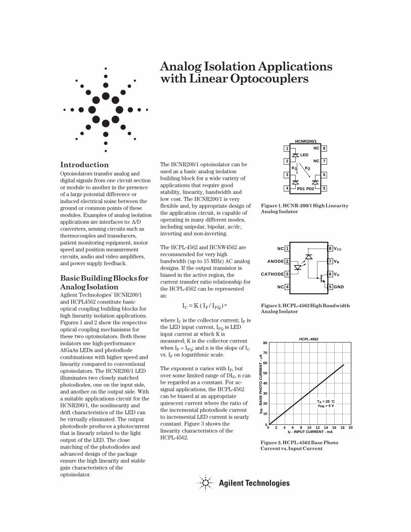
Analog Isolation Applicationswith Linear Optocouplers
Figure 1. HCNR-200/1 High Linearity
Analog Isolator
IntroductionOptoisolators transfer analog anddigital signals from one circuit sectionor module to another in the presenceof a large potential difference orinduced electrical noise between theground or common points of thesemodules. Examples of analog isolationapplications are interfaces to: A/Dconverters, sensing circuits such asthermocouples and transducers,patient monitoring equipment, motorspeed and position measurementcircuits, audio and video amplifiers,and power supply feedback.
Basic Building Blocks for
Analog IsolationAgilent Technologies’ HCNR200/1and HCPL4562 constitute basicoptical coupling building blocks forhigh linearity isolation applications.Figures 1 and 2 show the respectiveoptical coupling mechanisms forthese two optoisolators. Both theseisolators use high-performanceAlGaAs LEDs and photodiodecombinations with higher speed andlinearity compared to conventionaloptoisolators. The HCNR200/1 LEDilluminates two closely matchedphotodiodes, one on the input side,and another on the output side. Witha suitable applications circuit for theHCNR200/1, the nonlinearity anddrift characteristics of the LED canbe virtually eliminated. The outputphotodiode produces a photocurrentthat is linearly related to the lightoutput of the LED. The closematching of the photodiodes andadvanced design of the packageensure the high linearity and stablegain characteristics of theoptoisolator.
Figure 2. HCPL-4562 High Bandwidth
Analog Isolator
Figure 3. HCPL-4562 Base Photo
Current vs. Input Current
The HCNR200/1 optoisolator can beused as a basic analog isolationbuilding block for a wide variety ofapplications that require goodstability, linearity, bandwidth andlow cost. The HCNR200/1 is veryflexible and, by appropriate design ofthe application circuit, is capable ofoperating in many different modes,including unipolar, bipolar, ac/dc,inverting and non-inverting.
The HCPL-4562 and HCNW4562 arerecommended for very highbandwidth (up to 15 MHz) AC analogdesigns. If the output transistor isbiased in the active region, thecurrent transfer ratio relationship forthe HCPL-4562 can be representedas:
IC = K ( IF / IFQ ) n
where IC is the collector current; IF isthe LED input current, IFQ is LEDinput current at which K ismeasured; K is the collector currentwhen IF = IFQ; and n is the slope of ICvs. IF on logarithmic scale.
The exponent n varies with IF, butover some limited range of DIF, n canbe regarded as a constant. For ac-signal applications, the HCPL-4562can be biased at an appropriatequiescent current where the ratio ofthe incremental photodiode currentto incremental LED current is nearlyconstant. Figure 3 shows thelinearity characteristics of theHCPL-4562.
8
7
6
1
3
HCNR200/1
5
2
4
LED
NC
NC
PD1 PD2
K1 K2
8 VCC
7 VB
6 VO
5 GND
NC
ANODE
CATHODE
NC
1
2
3
4
80
70
60
50
40
30
20
10
00 2018161412108642
IF - INPUT CURRENT - mA
I PB
- B
AS
E P
HO
TO
CU
RR
EN
T -
µA
TA = 25 °CVPB > 5 V
HCPL-4562

50
ANALOG APPLICATIONSHigh Speed Isolation Amplifier
DescriptionThis is a high-speed, low-cost
isolation amplifier for use in the
feedback path of switch-mode
power supplies or motor speed
and position measurement. This
circuit can be used in applica-
tions where high bandwidth, low-
cost, and stable gain are required,
but where accuracy is not critical.
Performance ofOptocoupler• 1.5 MHz bandwidth
• Stable gain
• Low-cost support circuit
• Circuit couples only positive
voltage signals
Benefits
• Low cost solution for coupling
positive voltage analog signals
• Simple way for sending power
supply voltage feedback signal
across isolation barrier
ReferencesHCNR200/1 Technical Data
Alternative Agilent Parts
1) HCPL-7800A, HCPL-7800,
HCPL-7840 Isolation Amplifier
2) HCPL-4562 Wideband Analog/
Video Optocoupler
3) HCPL-785X Hermetically
Sealed Isolation Amplifier
VIN
VCC1 +5 V
R168 kΩ
PD1
LEDR310 kΩ
Q12N3906 R4
10 Ω
Q22N3904
VCC2 +5 V
R268 kΩ
PD2
R510 kΩ
Q32N3906
R610 Ω
Q42N3904
R7470
VOUT
8
7
6
1
3
HCNR200/1
5
2
4
LED
NC
NC
PD1 PD2
K1 K2ISOLATIONBARRIER
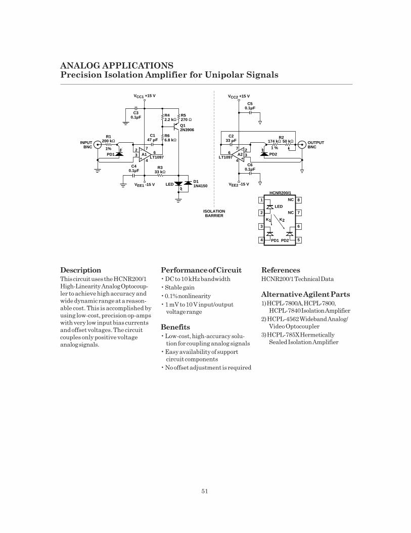
51
ANALOG APPLICATIONSPrecision Isolation Amplifier for Unipolar Signals
DescriptionThis circuit uses the HCNR200/1
High-Linearity Analog Optocoup-
ler to achieve high accuracy and
wide dynamic range at a reason-
able cost. This is accomplished by
using low-cost, precision op-amps
with very low input bias currents
and offset voltages. The circuit
couples only positive voltage
analog signals.
Performance of Circuit• DC to 10 kHz bandwidth
• Stable gain
• 0.1% nonlinearity
• 1 mV to 10 V input/output
voltage range
Benefits
• Low-cost, high-accuracy solu-
tion for coupling analog signals
• Easy availability of support
circuit components
• No offset adjustment is required
ReferencesHCNR200/1 Technical Data
Alternative Agilent Parts
1) HCPL-7800A, HCPL-7800,
HCPL-7840 Isolation Amplifier
2) HCPL-4562 Wideband Analog/
Video Optocoupler
3) HCPL-785X Hermetically
Sealed Isolation Amplifier
–
+PD1
23 A1
7
4
R1200 kΩINPUT
BNC 1%
C30.1µF
VCC1 +15 V
C147 PF
LT1097
R66.8 kΩ
R42.2 kΩ
R5270 ΩQ12N3906
VEE1 -15 V
C40.1µF
R333 kΩ
LEDD11N4150
–
+PD2
23A2
7
4
C233 PF OUTPUT
BNC174 kΩ
LT1097
50 kΩ1 %
VEE2 -15 V
C60.1µF
R2
C50.1µF
VCC2 +15 V
66
8
7
6
1
3
HCNR200/1
5
2
4
LED
NC
NC
PD1 PD2
K1 K2
ISOLATIONBARRIER

52
ANALOG APPLICATIONSIsolation Amplifier for Bipolar Signals - Circuit No. 1
DescriptionThis circuit shows how the
HCNR200 High Linearity Opto-
coupler can be used for transmit-
ting bipolar analog signals across
an isolation boundary. This
circuit uses two optocouplers:
OC1 and OC2; OC1 handles the
positive portions of the input
signal and OC2 handles the
negative portions. Diodes D1 and
D2 help reduce cross-over distor-
tion by keeping both amplifiers
active during both positive and
negative portions of the input
signal.
Performance of Circuit• 0.01% nonlinearity
• Bandwidth: dc to 100 Hz
• Low transfer gain variation: ±5%
(K3 of HCNR201)
Benefits• Low drift
• Low crossover distortion within
the dc to 100 Hz frequency band
• Good linearity
• Very low offset
ReferencesHCNR200/1 Technical Data
Alternative Agilent Parts
1) HCPL-7800A, HCPL-7800,
HCPL-7840 Isolation Amplifier
2) HCPL-785X Hermetically
Sealed Isolation Amplifier
–
+VOUT
–
+
VIN
OC1PD1
+
–
OC2PD1
R150 kΩBALANCE
D2
C2 10 pF
C1 10 pF
D1 R4680 Ω
R5680
OC1LED
OC2LED
R3180 kΩ
R2180 kΩ
C3 10 pF
OC1PD2
R6180 kΩ
R750 kΩ
GAIN
OC2PD2
8
7
6
1
3
HCNR200/1
5
2
4
LED
NC
NC
PD1 PD2
K1 K2ISOLATIONBARRIER
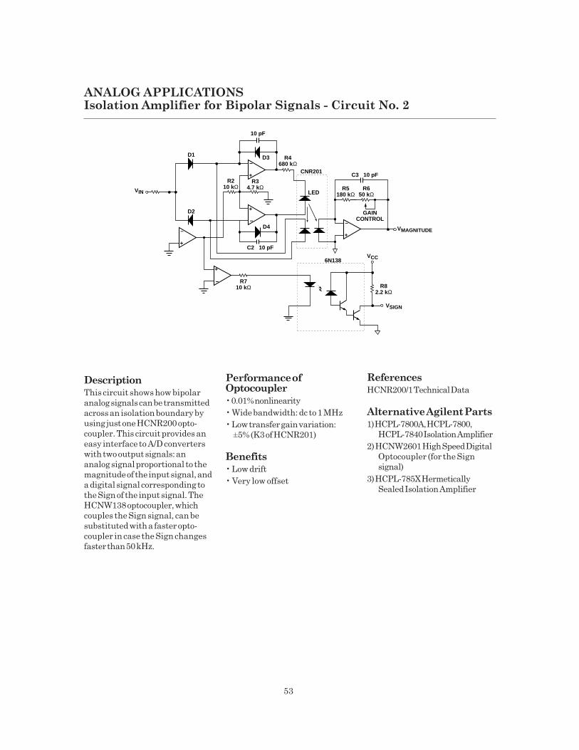
53
ANALOG APPLICATIONSIsolation Amplifier for Bipolar Signals - Circuit No. 2
DescriptionThis circuit shows how bipolar
analog signals can be transmitted
across an isolation boundary by
using just one HCNR200 opto-
coupler. This circuit provides an
easy interface to A/D converters
with two output signals: an
analog signal proportional to the
magnitude of the input signal, and
a digital signal corresponding to
the Sign of the input signal. The
HCNW138 optocoupler, which
couples the Sign signal, can be
substituted with a faster opto-
coupler in case the Sign changes
faster than 50 kHz.
ReferencesHCNR200/1 Technical Data
Alternative Agilent Parts1) HCPL-7800A, HCPL-7800,
HCPL-7840 Isolation Amplifier
2) HCNW2601 High Speed Digital
Optocoupler (for the Sign
signal)
3) HCPL-785X Hermetically
Sealed Isolation Amplifier
Performance ofOptocoupler
• 0.01% nonlinearity
• Wide bandwidth: dc to 1 MHz
• Low transfer gain variation:
±5% (K3 of HCNR201)
Benefits• Low drift
• Very low offset
–
+VMAGNITUDE
–
+
VIN
+
–GAIN
CONTROL
–
+
+
–
VCC
VSIGN
CNR201
LED
6N138
D4
10 pF
R4680 kΩ
R5180 kΩ
D1
D2
D3
R34.7 kΩ
R210 kΩ
R710 kΩ
C2 10 pF
C3 10 pF
R82.2 kΩ
R650 kΩ

54
ANALOG APPLICATIONSAC-Coupled Isolation Amplifier
DescriptionThis circuit with the HCPL-4562
Wideband Analog/Video
Optocoupler functions as an ac-
coupled isolation amplifier that
can be used for coupling audio or
video signals. The input circuit
biases the optocoupler LED at a
quiescent current of about 6 mA,
determined primarily by resistors
R1, R2, and R3. Diode D1 helps to
stabilize the operating point over
the operating temperature range.
An ac-coupled signal will modu-
late the collector current of
transistor Q1 and the optocoupler
LED. The output circuit consists
of a simple transresistance
(current-in, voltage-out) amplifier
followed by a common-emitter
amplifier stage.
Performance of Circuit• Typical bandwidth: 13 MHz
• Nominal gain of circuit: 1
• Isolation-mode rejection: 46 dB
at 1 kHz
• Overall nonlinearity: 0.5%
• Optocoupler input current
range: 4 mA-8 mA
Benefits• Simple solution for coupling
audio and video signals
References1) HCPL-4562 Wideband
Analog/Video Optocoupler
Technical Data
2) Application Note 951-2,
“Linear Applications of
Optocouplers”
Alternative AgilentParts1) HCPL-2502, 6N135, 6N136
High Speed Transistor
Output Optocouplers
2) HCNW4562 Widebody Wide-
band Analog/Video Optocoupler
3) HCPL-55XX, 4N55,
HCPL-6530/1 Hermetically
Sealed High Speed
Optocoupler
4) HCPL-05XX Small-Outline
High Speed Optocoupler
7
5
6
8
2
3
4
1
HCPL-4562+5 V
R55.6 kΩ
KPD
Q2
R7470 Ω
ID
2 µFQ3
R682 Ω
2
R418 kΩ
2 µF
Q1
R3330 Ω
1
R21.8 kΩ
+5 V
R12.2 kΩ
VIN
IF
D11N4150
Q1 2N3904Q3 2N3904
GAIN 1 • KPD • R4 • R7 1
KPD = 0.0032 TYPICALLY
R3 R6
I3
VOUT

55
Isolated Video Interface
DescriptionThis circuit, with the HCPL-4562
Wideband Analog/Video
Optocoupler, is optimized for
video signal coupling. The peaked
response of the detector circuit
helps extend the frequency range
over which the gain is relatively
constant. The number of gain
stages, the overall circuit
topology, and the dc bias points
are all chosen to maximize the
bandwidth.
Performance of Circuit• Typical bandwidth: 15 MHz
• Typical Gain variation: -1.1 dB
at 5 MHz with reference at 0.1
MHz
• Isolation Mode Rejection:
122 dB at 120 Hz
Benefits• Cost-effective, high perfor-
mance video interface circuit
ReferencesHCPL-4562 Wideband Analog/
Video Optocoupler Technical
Data
Alternative Agilent Parts
HCNW4562 Widebody Wideband
Analog/Video Optocoupler
HCPL-4562

Inverter Design UsingGate Drive and Current SenseOptocouplers
System OverviewA typical motor drive and power
control system shown in Figure 1
requires isolation between the
high voltage devices (IGBT/
MOSFET) and the low voltage
devices (micro-controller). In
addition to meeting the severe
requirements for the isolation
function, Agilent Technologies
optocouplers provide customized
functionality such as direct gate
drive for IGBTs or power
MOSFETs, and analog isolation
for motor current sensing, voltage
sensing, speed measurement, and
position measurement.
VOLTAGESENSE
MICRO-CONTROLLER
CURRENTSENSE
CURRENTSENSE
GATEDRIVE
GATEDRIVE
B
A
3- PHASEOUTPUT
U+
U-
V+
V-
W+
W-
+HV
C
-HV
ANALOGISOLATION
MOTOR SPEED, POSITION
A, B, CU+, U-, V+, V-, W+, W-
GATEDRIVE
GATEDRIVE
GATEDRIVE
GATEDRIVE
Figure 1. Isolation Circuits for Power Control – System Overview
Isolated Gate Drive and
IPM InterfaceMany motor drive and power
control systems use pulse width
modulation switching of power
devices to generate a three phase
variable voltage and variable
frequency power source. High
performance motor drives require
precision timing for turning on
and turning off the power devices
on the inverter. The micro-
controller that controls the turn-
on and turn-off of these power
devices needs to be isolated from
the high voltage inverter
side. Agilent Technologies offers
a variety of optocouplers that
have built-in gate drive capability.
For solutions that require only a
simple isolation interface, Agilent
provides Intelligent Power
Module (IPM) interface
optocouplers. All of Agilent’s gate
drive and IPM interface
optocouplers meet stringent
industrial requirements with
critical performance:
• Minimum Common Mode
Rejection: 10 kV/µs slew rate
at 1,500 V peak transients
• Wide Operating Temperature
Range: -40°C to +85°C
• Over Current Protection and
Fault Feedback (HCPL-316J)
• Safety Standards Certifications:
UL, CSA, VDE
• Fast Switching Speeds: 500 ns
range (see detailed part
number specifications)
• Wide Supply Voltage Range:
15 V to 30 V

57
MOTOR CONTROL APPLICATIONS
Isolated Current and
Voltage SensingAgilent Technologies provides
several analog isolation amplifier
products for isolated precision
current and voltage sensing for
monitoring motor performance.
Agilent also offers a digital output
isolation amplifier for direct
connection to a micro-controller.
Compared to Hall-Effect sensors,
Agilent’s isolation amplifiers have
excellent gain and offset
characteristics, especially very
low offset drift over a wide
temperature range. In addition,
they provide a compact, low-cost,
and reliable solution for motor
drive designers that need to
accurately measure motor voltage
and current. Some of the key
performance features include:
• 12-bit linearity (HCPL-7860)
• over current detection (HCPL-
788J)
• ±200 mV input range
• -40°C to +85°C operating
temperature range
• 15 kV/µs isolation transient
immunity
• Safety Standards Certifications:
UL, CSA, VDE
Analog Signal Isolation
for Speed and Position
MeasurementAgilent Technologies offers a low
cost, high accuracy, isolated
amplifier solution for the
measurement of speed and
position in a motor. With the use
of Agilent Technologies’
HCNR201 and low cost
operational amplifiers, circuit
designers have the flexibility of
designing analog isolation
amplifiers that have low input
bias currents, high bandwidth,
stable gain, and very high
linearity.
Common Mode RejectionThe detector shield in the
optocoupler prevents CMR failure
due to capacitive coupling from
the input side of the optocoupler,
through the package, to the
detector IC. However, this shield
does not eliminate the capacitive
coupling between the LED and
the optocoupler output pins and
output ground as shown in Figure
2. This capacitive coupling causes
perturbations in the LED current
during common mode transients
and becomes the major source of
CMR failures for a shielded
optocoupler. The main design
objective of a high CMR LED
drive circuit becomes keeping the
LED in the proper state (on or
off) during common mode
transients. The recommended
application circuits for Agilent’s
gate drive applications can
achieve 15 kV/µs CMR while
minimizing component
complexity.
Another cause of CMR failure for
a shielded optocoupler is direct
coupling to the optocoupler
output pins through CLED01 and
CLED02 in Figure 2. Many factors
influence the effect and
magnitude of the direct coupling
Figure 2. AC Equivalent for a Digital
Optocoupler
including: the use of an internal
or external output pull-up
resistor, the position of the LED
current setting resistor, the
connection of the unused input
package pins, and the value of
the capacitor at the optocoupler
output (CL). The recommended
gate drive and IPM interface
application circuits for
Agilent optocouplers have been
optimized to reduce the
likelihood of CMR failure.
IPM Dead Time and
Propagation Delay
SpecificationsMany of Agilent’s gate drive and
IPM interface optocouplers
include a Propagation Delay
Difference (PDD) specification
intended to help designers
minimize “dead time” in their
power inverter designs. Dead
time is the time periods during
which both the high and low side
power transistors (Q1 and Q2) of
a power module are off. Any
overlap in Q1 and Q2 conduction
will result in large currents
flowing through the power
devices between the high and low
voltage motor rails.
To minimize dead time the
designer must consider the
propagation delay characteristics
of the optocoupler as well as the
characteristics of the IGBT gate
drive circuit. Considering only
the delay characteristics of the
optocoupler (the characteristics
of the IGBT gate drive circuit can
be analyzed in the same way) it is
important to know the minimum
and maximum turn-on (tPHL ) and
turn-off (tPLH ) propagation delay
specifications, preferably over
the desired operating
temperature range.
1
2
SHIELD
8
7
6
5
3
4
20 kΩCLEDP
CLEDN
CLED02
CLED01

58
The limiting case of zero dead
time occurs when the input to Q1
turns off at the same time that the
input to Q2 turns on. This case
determines the minimum delay
between LED1 turn-off and LED2
turn-on, which is related to the
worst case optocoupler
propagation delay waveforms, as
shown in Figure 3. A minimum
dead time of zero is achieved in
Figure 3 when the signal to
turn on LED2 is delayed by
(tPLH max - tPHL min ) from the LED1
turn off. Note that the
propagation delays used to
calculate PDD are taken at equal
temperatures since the
optocouplers under consideration
are typically mounted in close
proximity to each other.
(Specifically, tPLH max and
tPHLmin in the Figure 3 equations
are not the same as the tPLH max
and tPHL min, over the full
operating temperature range,
specified in the data sheet.).
This delay is the maximum value
for the propagation delay
difference specification that is
specified at 450 ns for the HCPL-
4506 over an operating
temperature range of -40°C to
+100°C. Delaying the LED signal
by the maximum propagation
delay difference ensures that the
minimum dead time is zero, but it
does not tell a designer what the
maximum dead time will be. The
maximum dead time occurs in the
highly unlikely case where one
optocoupler with the fastest tPLH
and another with the slowest tPHL
are in the same inverter leg. The
maximum dead time in this case
becomes the sum of the spread in
the tPLH and tPHL propagation
delays as shown in Figure 3.
Figure 3. Propagation Delay and Dead Time
The maximum dead time is also
equivalent to the difference
between the maximum and
minimum propagation delay
difference specifications. The
maximum dead time (due to the
optocouplers) for the HCPL-4506
is 600 ns over an operating
temperature range of -40°C to
+100°C.
tPHLMIN.
ILED2
ILED1
VOUT1VOUT2
tPLHMIN.
tPLHMAX.
tPHLMAX.
PDD*MAX.
MAX.DEAD TIME
Q1 ON
Q2 OFFQ2 ON
Q1 OFF
MAXIMUM DEAD TIME (DUE TO OPTOCOUPLER)
= (tPLH MAX. - tPLH MIN.) + (tPHL MAX. - tPHL MIN.)
= (tPLH MAX. - tPHL MIN.) + (tPLH MIN. - tPHL MAX.)
= PDD* MAX. - PDD* MIN.
PROPAGATION DELAY DIFFERENCE (PPD) MAX.
= (tPLH - tPHL) MAX. = (tPLH MAX. - tPHL MIN.)
NOTE: THE PROPAGATION DELAYS USED TO CALCULATE THEPDD AND MAXIMUM DEAD TIME ARE TAKEN AT EQUAL TEMPERATURES.
MOTOR CONTROL APPLICATIONS

59
Bootstrap Power Supply
Circuit for Power
Control SystemsFigure 4 shows a bootstrapped
output power supply circuit that
has the following benefits:
• eliminates the need for an
isolated power supply or a dc-
to-dc converter,
• lower cost solution compared
to transformer based power
supply,
• less printed circuit board
space.
This circuit includes a bootstrap
circuit for providing output
power to the HCPL-316J gate
drive optocouplers, thereby
Figure 4. Bootstrap Circuit for Power Control System
eliminating the need for isolated
power supplies or dc-to-dc
converters. It can be modified to
suit other Agilent gate drive
optocouplers and current/voltage
sensing isolation amplifiers.
Component values were chosen
for a 350 V rail =
HV+ - HV - (240 V x 1.414).
When the lower IGBT is turned
on, VC1H charges up (through
D1H ) to a voltage of:
VC1H = HV+ - [HV- + VSATM2+ VCC2H + VF (D1H )]
= 350 V - 3 V - 18 V - 1 V
= 328 V
161514131211109
12345678
VIN+VIN–VCC1GND1RESETFAULTVLED1+VLED1–
VEVLED2+DESAT
VCC2VC
VOUTVEEVEE
HIGH GATE-DRIVE
(LOW GATE-DRIVE CIRCUIT ISIDENTICAL TO HIGH
GATE-DRIVE CIRCUIT)
HCPL-316J
161514131211109
12345678
VIN+VIN–VCC1GND1RESETFAULTVLED1+VLED1–
VEVLED2+DESAT
VCC2VC
VOUTVEEVEE
LOW GATE-DRIVE
HCPL-316J
N/C
RTONH10
RBIASDH20K
VCC2(H)
VDESAT(H)
VC(H)VO(H)
VE(H)
VEE(H)
DZLH18 V
C2H1.2 µF(20%)
C3H0.1 µF
1 kRDESATH
RGH12.5
DZ2H12 V
C4H250 nF
D2HA14P
1,000 V
R1L47K
R2L20
15nFC1L
1KRDESATL
DDSLHV DIODE
RGL12.5
DFBLO(DSE130-12A,
IXYS)
HV–
ACMOTOR
DFBHI(DSE130-12A,
IXYS)
DDSHA14P
1,000 V
HV+DUAL IGBT
R2H20
15 nFC1H
HV+HV+
R1H47K
D1HA14P
1,000 V
M1
M2
MOTOR CONTROL APPLICATIONS

60
where VSATM2 is the saturation or
“on” voltage across the collector-
emitter of IGBT M2; VF (D1H) is the
voltage across diode DD1H ; and
HV+, HV- are the rail voltages.
When M2 (low IGBT) switches off
and M1 (upper IGBT) switches
on, VE(H) pulls up to HV+ -VSATM1.
This causes C4H to become
charged through D2H. Charge
sharing between C1H and C4H
results in the voltage across C4H
which (in the absence of
clamping diode DZ2H ) can be
approximated by:
C4H × ∆VC4H = C1H × 328 V
∆VC4H = 19.6 V
where ∆VC4H = the voltage drop
across C4H . The negative gate
bias then is held at 12 V by
clamping Zener DZ2H.
Shunt Resistor Selection
for Current SensingThe current-sensing shunt
resistor should have low
resistance to minimize power
dissipation, low inductance to
minimize di/dt induced voltage
spikes which could adversely
affect operation, and reasonable
tolerance to maintain overall
circuit accuracy. Choosing a
particular value for the
shunt is usually a compromise
between minimizing power
dissipation and maximizing
accuracy. Smaller shunt
resistance decrease power
dissipation, while larger shunt
resistance can improve circuit
accuracy by utilizing the full input
range of the isolated modulator.
Agilent Technologies
recommends Dale Electronics’
two-terminal shunt resistors for
low cost applications. These
resistors are suitable for
measuring current up to 28 Arms .
See comparison table below.
Several four-terminal shunts
from Isotek suitable for sensing
currents in motor drives up to 71
Arms (71 hp or 53 kW) are shown
in the comparison table below;
the maximum current and motor
power range for each of the
PBV-series shunts are indicated.
For shunt resistance from 50 mW
down to 10 mW, the maximum
current is limited by the input
voltage range of the isolated
modulator. For the 5 mW and
2 mW shunts, a heat sink may be
required due to the increased
power dissipation at higher
currents.
Shunt Resistor Shunt Unit Price Tolerance Temp. Max. RMS Motor Power Range
Part Number Resistance @ 2500 Qty. Coefficient Current 120 Vac - 440 Vac
(mΩ) (US$) ( % ) (ppm/°C) (A) (hp) (kW)
PBV-R050-0.5 50 $3.74 0.5 <30 3 0.8 - 3 0.6 - 2
PBV-R020-0.5 20 $3.74 0.5 <30 7 2 - 7 1.4 - 5
PBV-R010-0.5 10 $3.74 0.5 <30 14 4 - 14 3 - 10
PBV-R005-0.5 5 $4.09 0.5 <30 25 [28] 7-25 [8-28] 5-19 [6-21]
PBV-R002-0.5 2 $4.09 0.5 <30 39 [71] 11 - 39 8 - 29[19 - 71] [14 - 53]
High Performance Four-Terminal Shunt Resistor Selection Guide (Supplier: Isotek, Tel: 508-673-2900)
Note: Values in brackets are with a heatsink for the shunt.
Shunt Resistor Shunt Price Tolerance Temp. Max. RMS Motor Power Range
Part Number Resistance Range Coefficient Current 120 Vac - 440 Vac
(mΩ) (US$) ( % ) (ppm/°C) (A) (hp) (kW)
LV-5.005 5 $0.40 - 1.00 1 <300 28.3 8 - 28 6 - 21
LVR-3.01 10 $0.38 - 0.76 1 <300 14.1 4 - 14 3 - 10
LVR-3.02 20 $0.38 - 0.76 1 <300 7 2 - 7 1.4 - 5
LVR-3.05 50 $0.38 - 0.76 1 <300 2.8 0.8 - 3 0.6 - 2
WSC-2.02* 20 $0.38 - 0.76 1 <300 7.1 2 - 7 1.4 - 5
Low Cost Two Terminal Resistor Selection Guide (Supplier: Dale Electronics, Tel: 402-564-3131)
* Surface Mount
MOTOR CONTROL APPLICATIONS
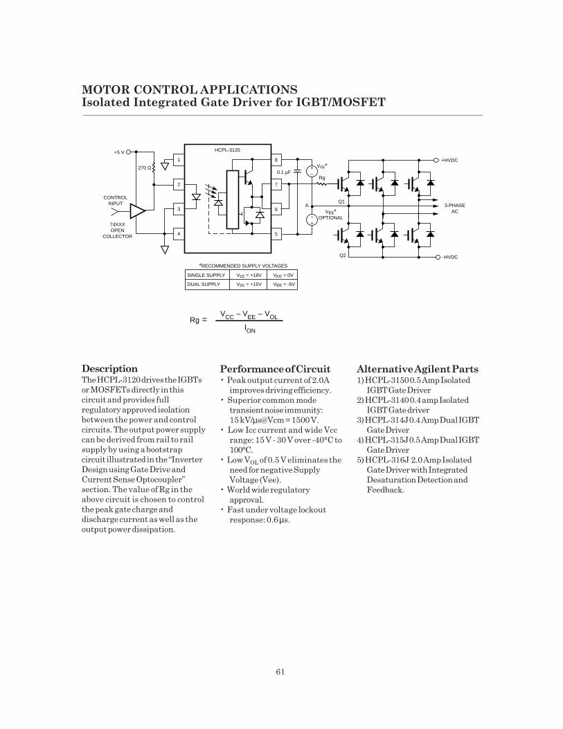
61
MOTOR CONTROL APPLICATIONSIsolated Integrated Gate Driver for IGBT/MOSFET
DescriptionThe HCPL-3120 drives the IGBTs
or MOSFETs directly in this
circuit and provides full
regulatory approved isolation
between the power and control
circuits. The output power supply
can be derived from rail to rail
supply by using a bootstrap
circuit illustrated in the “Inverter
Design using Gate Drive and
Current Sense Optocoupler”
section. The value of Rg in the
above circuit is chosen to control
the peak gate charge and
discharge current as well as the
output power dissipation.
Performance of Circuit• Peak output current of 2.0A
improves driving efficiency.
• Superior common mode
transient noise immunity:
15 kV/µs@Vcm = 1500 V.
• Low Icc current and wide Vcc
range: 15 V - 30 V over -40°C to
100°C.
• Low VOL of 0.5 V eliminates the
need for negative Supply
Voltage (Vee).
• World wide regulatory
approval.
• Fast under voltage lockout
response: 0.6 µs.
Alternative Agilent Parts1) HCPL-3150 0.5 Amp Isolated
IGBT Gate Driver
2) HCPL-3140 0.4 amp Isolated
IGBT Gate driver
3) HCPL-314J 0.4 Amp Dual IGBT
Gate Driver
4) HCPL-315J 0.5 Amp Dual IGBT
Gate Driver
5) HCPL-316J 2.0 Amp Isolated
Gate Driver with Integrated
Desaturation Detection and
Feedback.
1
2
CONTROLINPUT
8
Rg7
Q1
6
*RECOMMENDED SUPPLY VOLTAGES
5
3
4
+–
+–
74XXXOPEN
COLLECTOR
+5 V
270 Ω
HCPL-3120
Vcc*
VEE*OPTIONAL
0.1 µF
Q2
A
+HVDC
–HVDC
3-PHASEAC
SINGLE SUPPLY Vcc = +18V VEE = 0V
DUAL SUPPLY Vcc = +15V VEE = -5V
Rg =VCC – VEE – VOL
ION
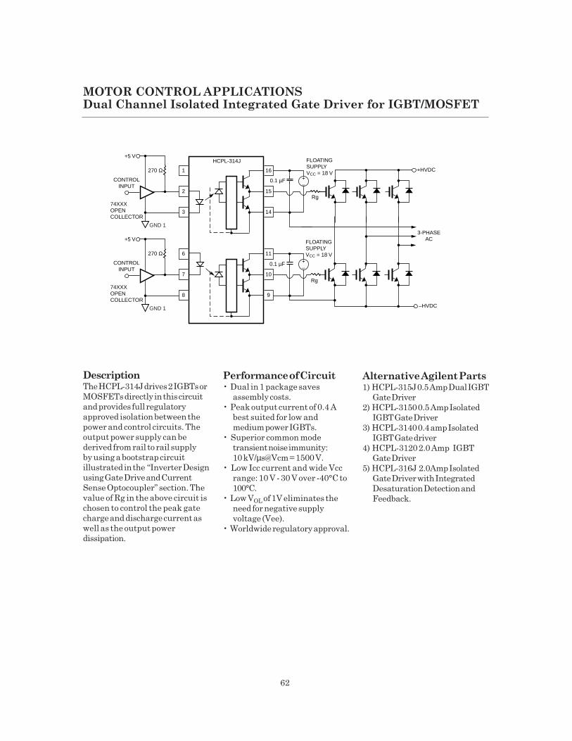
62
MOTOR CONTROL APPLICATIONSDual Channel Isolated Integrated Gate Driver for IGBT/MOSFET
DescriptionThe HCPL-314J drives 2 IGBTs or
MOSFETs directly in this circuit
and provides full regulatory
approved isolation between the
power and control circuits. The
output power supply can be
derived from rail to rail supply
by using a bootstrap circuit
illustrated in the “Inverter Design
using Gate Drive and Current
Sense Optocoupler” section. The
value of Rg in the above circuit is
chosen to control the peak gate
charge and discharge current as
well as the output power
dissipation.
Performance of Circuit• Dual in 1 package saves
assembly costs.
• Peak output current of 0.4 A
best suited for low and
medium power IGBTs.
• Superior common mode
transient noise immunity:
10 kV/µs@Vcm = 1500 V.
• Low Icc current and wide Vcc
range: 10 V - 30 V over -40°C to
100°C.
• Low VOL of 1V eliminates the
need for negative supply
voltage (Vee).
• Worldwide regulatory approval.
Alternative Agilent Parts1) HCPL-315J 0.5 Amp Dual IGBT
Gate Driver
2) HCPL-3150 0.5 Amp Isolated
IGBT Gate Driver
3) HCPL-3140 0.4 amp Isolated
IGBT Gate driver
4) HCPL-3120 2.0 Amp IGBT
Gate Driver
5) HCPL-316J 2.0Amp Isolated
Gate Driver with Integrated
Desaturation Detection and
Feedback.
CONTROLINPUT
FLOATINGSUPPLYVCC = 18 V
FLOATINGSUPPLYVCC = 18 V
74XXXOPENCOLLECTOR
+5 V
270 Ω
HCPL-314J
+HVDC
–HVDC
3-PHASEAC
16
Rg
Rg
0.1 µF
0.1 µF
15
14
1
2
3
11
10
9
6
7
8
+–
+–
GND 1
CONTROLINPUT
74XXXOPENCOLLECTOR
+5 V
270 Ω
GND 1

63
MOTOR CONTROL APPLICATIONSIsolated Gate Drive for IGBT/MOSFET with IntegratedDesaturation Protection and Fault Feedback
DescriptionThe HCPL-316J drives IGBTs or
MOSFETs directly and provides
additional IGBT desaturation
protection. The Vce of the IGBT
is monitored by Desat pin and
the IGBT will be slowly turned off
if Vdesat exceeds a threshold of
7 V. A fault feedback signal is
propagated to the input side to
notify the micro-controller of the
detected fault condition. This
FAULT output remains low until
the part is reset. The 100 pF
blanking capacitor shown in the
diagram above will delay the rise
of VDesat for a period of around
4 µs to allow the IGBT sufficient
time to turn on and the collector
to settle to a low VDesat.
Performance of Circuit• Gate Drive Current : 2.0 A
• Common mode Transient
Rejection: 15 kV/µs@VCM =
1.5 kV
• IGBT gate protection response
time: 3 µs.
• IGBT fault signal propagation
delay: 10 µs.
Benefits:• Reduced assembly costs
• CMOS/TTL compatible
• Local IGBT soft shutdown
• Worldwide regulatory approval
Alternative Agilent Parts1) HCPL-315J 0.5 Amp Dual IGBT
Gate Driver
2) HCPL-3150 0.5 Amp Isolated
IGBT Gate Driver
3) HCPL-J314 0.4 amp Isolated
IGBT Gate driver
4) HCPL-314J 0.4 Amp Dual IGBT
Gate Driver
5) HCPL-3120 2.0Amp Isolated
Gate Driver.
3-PHASEOUTPUT
161514131211109
12345678
VIN+VIN–VCC1GND1RESETFAULTVLED1+VLED1–
VEVLED2+DESAT
VCC2VC
VOUTVEEVEE
HCPL-316J
20k
1k
20k
300 pF
DESATFAULT
(OUTPUT)
MICRO-CONTROLLERVCC15 V
DRIVESIGNAL(INPUT)
RESET(INPUT)
74ACT04
0.1 µF 3.3 k
0.1 µF
0.1 µF
0.1 µF
VCC2-5 V
VCC218 V
HV DIODE
RDESATH
RGATEH
Rg =VCC – VEE – VOL
ION

64
MOTOR CONTROL APPLICATIONSIsolated Interface for Intelligent Power Module Gate Drive
DescriptionThe HCPL-4506 provides isolation
between the controller and the
IPM (Intelligent Power Module).
This optoisolator provides world
wide safety certification (UL,
CSA, VDE, BSI). The HCPL-4506
optocouplers can reject common
mode transients that have slew
rates as high as 15 kV/µs and
peak voltage up to 1500 V.
Furthermore, this optocoupler
has guaranteed Pulse Width
Distortion and Propagation Delay
Difference specifications that
allow the circuit designer to
reduce switching dead time and
improve inverter efficiency.
Performance of
Optocoupler• Minimum 15 kV/µs transient
immunity
• Maximum propagation delay:
500 ns
• Maximum propagation delay
difference between any two
HCPL-4506s: 450 ns
• Specification guaranteed over
-40°C to 100°C operating
temperature range.
Benefits• World wide regulatory approval.
• Reduced deadtime
Alternative Agilent Parts1) HCNW4506 widebody,
VIORM = 1414 V, HCPL-J456,
VIORM = 891 V, HCPL-0456, SO8
package.
2) HCPL-4504, CNW4504, HCPL-
J454, HCPL-0454.
3) HCPL-4503, HCNW4503, HCPL-
0453.
1
2
SHIELD
SHIELD
8
7
6
5
3
4
HCPL-4506
0.1 µF20 KΩ20 KΩ
20 KΩ
310 Ω
310 Ω
20 kΩ
1
2
8
7
6
5
3
4
HCPL-4506
0.1 µF
HCPL-4506
HCPL-4506
HCPL-4506
HCPL-4506
+5 V
+5 V
CMOS
CMOS
VCC1
ILED1
ILED2
VOUT1
VOUT2
VCC2
M
+HV
–HV
Q1
Q2
HCPL-4506
IPM

65
MOTOR CONTROL APPLICATIONSLow Cost Isolated Phase Current Sensing with Analog Output
DescriptionThe HCPL-7840 Isolation
Amplifier can be used for
isolating the motor current
sensing element from the
control circuit while at the same
time transmitting precision
analog signals. This circuit
requires a low cost shunt resistor
for monitoring the motor current.
The voltage across the sensing
resistor is fed to the HCPL-7840
input pins 2 and 3. A floating
power supply (which in many
applications could be the same
one used to drive the high side
power transistors) is regulated to
5 V using a simple three-terminal
voltage regulator, 78L05. The
differential output from the
HCPL-7840 isolation amplifier is
converted to a ground-referenced
single-ended output voltage with
a simple differential amplifier
circuit (MC34082A and associated
components).
Performance of Circuit• Sense current: Up to 200 A
• Optocoupler bandwidth:
Up to 100 kHz
• Optocoupler nonlinearity: 0.2%
• Optocoupler input offset
voltage: 0.2 mV (typical)
• Optocoupler common-mode
rejection: 15 kV/µs
Benefits• Small size and lower profile
circuit compared to Hall-Effect
device current sensing circuits.
• Industry standard low profile
components are used in this
circuit.
• High precision measurement
while maintaining common
mode transient immunity.
Alternative Agilent Parts1) HCPL-7800A: 1% part-to-part
gain tolerance, HCPL-7800: 3%
part-to-part gain tolerance.
2) HCPL-788J: single ended
output isolation amplifier with
integrated over current
detection.
3) HCPL-7860 and HCPL-7870/
HCPL-0870: isolated 15 bit A/D
converter.
4) HCPL-786J: isolated 15 bit A/D
converter.
2.00 kΩ
10.0 kΩ
10.0 kΩ
2.00 kΩ
0.1 µF0.1 µF 0.1 µF
0.1 µF
0.1 µF
0.01µF
VOUT
RSENSE
M
IN OUT
78L05
HV+
+SUPPLY
39 Ω
1
2
3
4
88
76
5
4
7
150 pF
150 pF
6
5
HV–
+5 V
+5 V
-15 V
+15 V
+ –
–
+ MC34082A
HCPL-7840

66
MOTOR CONTROL APPLICATIONSIsolated A/D Converter for Phase Current Sensing
DescriptionThe HCPL-7860 Isolated
Modulator and the HCPL-x870
Digital Interface IC together form
an isolated programmable two-
chip analog-to-digital converter.
The isolated modulator allows
direct measurement of motor
phase currents in power inverters
while the digital interface IC can
be programmed to optimize the
conversion speed and resolution.
Performance of Circuit• Resolution due to linearity:
12 bits at tDELAY = 18 µs,
14 bits at tDELAY = 94 µs
• Common-mode transient
rejection: dV/dt = 15 kV/µs @
VCM = 1500 V
• Signal-to-Noise: SNR = 62 dB
(minimum)
• Regulatory Isolation Ratings:
VISO = 3750 V (per UL 1577),
VIORM = 848 V; VIOTM = 6000 V
• Input Offset Drift: 4 µV / °C
(typical)
• Reference Voltage Tolerance:
±4% (±1% within shipment
tube)
Benefits• Integrated analog-to-digital
converter means fewer
components required.
• High common-mode transient
rejection ensures no
corruption of data.
• Low gain temperature-
coefficient and offset voltage
ensure high accuracy
measurements.
References1) HCPL-7860/x870 Technical
Data
2) High precision current sensing
resistor suppliers: Dale in USA;
Isabellenhutte in Germany;
and PCN in Japan
+ -MOTOR
HV-
HV+
RSENSE
FLOATINGPOSITIVESUPPLY
GATE DRIVECIRCUIT
VDD1
VIN+
VIN-
GND1
VDD2
MCLK
MDAT
GND2
CDAT SCLK
CCLK VDD
CLAT CHAN
MCLK1 SDAT
MDAT1 CS
MCLK2 THR1
MDAT2 OVR1
GND RESET
+ 5 V
HCPL-7860
TOCONTROLCIRCUIT
C30.1 µF
C10.1 µF
C20.01 µF
R2 39 Ω
R1
D15.1 V
HCPL-X870
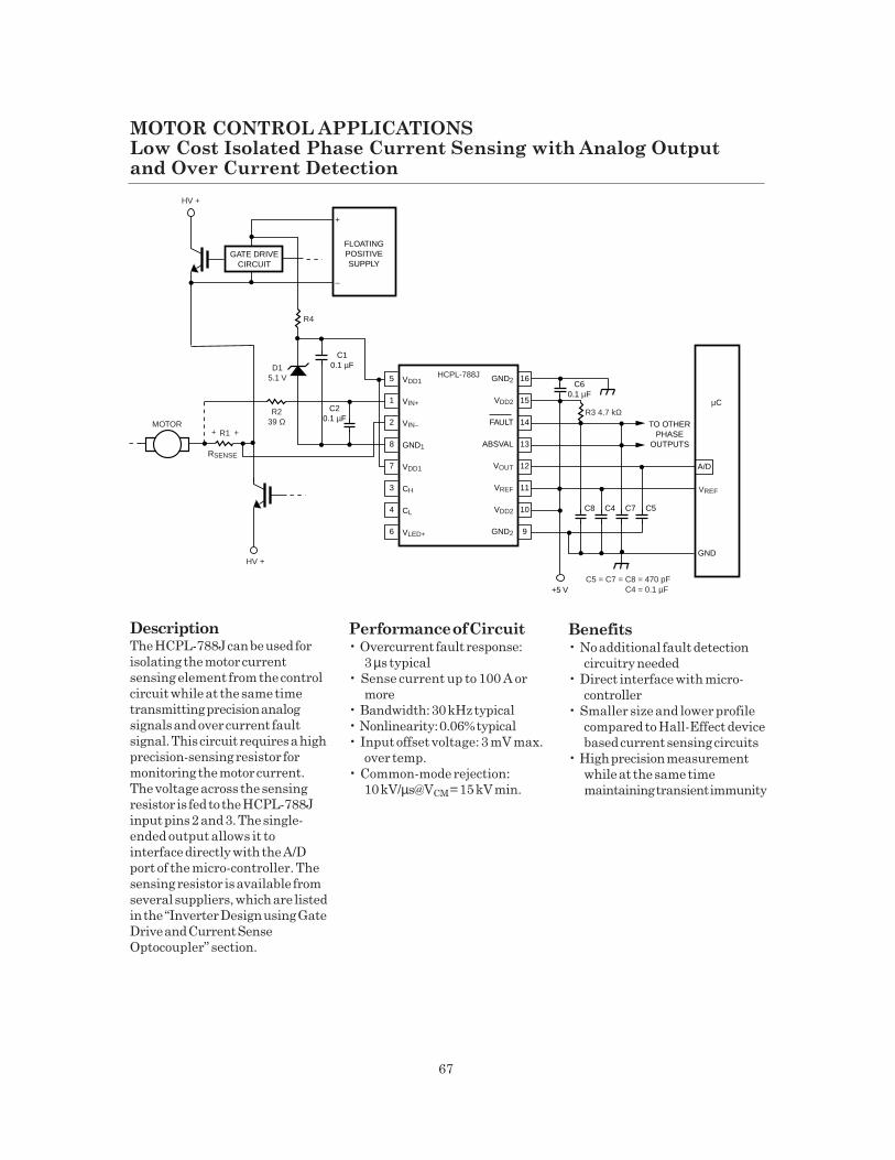
67
MOTOR CONTROL APPLICATIONSLow Cost Isolated Phase Current Sensing with Analog Outputand:Over Current Detection
DescriptionThe HCPL-788J can be used for
isolating the motor current
sensing element from the control
circuit while at the same time
transmitting precision analog
signals and over current fault
signal. This circuit requires a high
precision-sensing resistor for
monitoring the motor current.
The voltage across the sensing
resistor is fed to the HCPL-788J
input pins 2 and 3. The single-
ended output allows it to
interface directly with the A/D
port of the micro-controller. The
sensing resistor is available from
several suppliers, which are listed
in the “Inverter Design using Gate
Drive and Current Sense
Optocoupler” section.
Performance of Circuit• Overcurrent fault response:
3 µs typical
• Sense current up to 100 A or
more
• Bandwidth: 30 kHz typical
• Nonlinearity: 0.06% typical
• Input offset voltage: 3 mV max.
over temp.
• Common-mode rejection:
10 kV/µs@VCM = 15 kV min.
Benefits• No additional fault detection
circuitry needed
• Direct interface with micro-
controller
• Smaller size and lower profile
compared to Hall-Effect device
based current sensing circuits
• High precision measurement
while at the same time
maintaining transient immunity
5
FLOATINGPOSITIVESUPPLY
1
2
8
7
3
4
6
16
15
14
C8
13
12
11
10
9
GND2
VDD2
FAULT
ABSVAL
VOUT
VREF
VDD2
GND2
VDD1
VIN+
VIN–
GND1
VDD1
CH
CL
VLED+
A/D
TO OTHERPHASE
OUTPUTS
GATE DRIVECIRCUIT
C4 C7 C5
R3 4.7 kΩ
C60.1 µF
+5 V
GND
C5 = C7 = C8 = 470 pFC4 = 0.1 µF
VREF
µC
HCPL-788J
C10.1 µF
C20.1 µF
D15.1 V
R239 Ω
R1
HV +
++
RSENSE
MOTOR
HV +
+
–
R4

68
MOTOR CONTROL APPLICATIONSIsolated Inverter Rail Voltage Sensing using an Isolation Amplifier
DescriptionThe HCPL-7840 isolation
amplifier can be used for sensing
the rectified dc power supply
voltage in a power inverter. An
isolated 5 V power supply
regulated to 5 V using a simple
three-terminal voltage regulator
powers the HCPL-7840 input
circuit. The resistor divider
network is used so that the
full scale voltage at the HCPL-
7840 input is 200 mV. The
impedance of the resistor divider
must be less than 1 kΩ so that the
input resistance (500 kΩ) and
input bias current (1 mA) of the
isolation amplifier do not affect
the accuracy of the measurement.
To obtain higher bandwidths, the
input bypass capacitor (across
HCPL-7840’s pins 2 and 3 ) can be
reduced, but it should not be
reduced much below 1000 pF to
maintain gain accuracy of the
isolation amplifier.
Performance of Circuit• 15 kV/µs transient rejection
• 0.05% nonlinearity
• 5% gain tolerance
Benefits• Few components
• High electrical noise immunity
Agilent Alternative Parts1) HCPL-786J: isolated 15 bit A/D
converter
References1) HCPL-7860/x870 Technical
Data
2) High precision current sensing
resistor suppliers: Dale in USA;
Isabellenhutte in Germany;
and PCN in Japan
2.00 kΩ
10.0 kΩ
10.0 kΩ
2.00 kΩ
0.1 µF0.1 µF 0.1 µF
0.1 µF
0.1µF
VOUT
IN OUT
78L05
HV+
R1
+SUPPLY
39R2
1
2
3
4
88
76
5
4
7
150 pF
150 pF
6
5
HV–
+5 V
+5 V
-15 V
+15 V
–
+ MC34082A
HCPL-7840

69
Description
The HCPL-4562 Linear
Optocoupler is used in a servo
circuit to sense the rectified dc
power supply voltage of a power
inverter. The series resistor R1
limits the current that drives the
input LED of optocoupler U1. The
forward current through the LED
of the HCPL-4562 optocoupler is
proportional to the dc high
voltage power supply rail.
When the circuit is balanced with
the potentiometer R3, the output
voltage VO is proportional to the
high voltage dc power supply as
shown by the equation:
VO / VI = R2 / R1
Performance of Circuit• 122 dB isolation mode rejection
ratio
• 0.25% nonlinearity
• ±0.3%/°C gain variation
temperature coefficient
Benefits
• No isolated 5 V input power
supply is required for
optocoupler U1
• Simple circuit
Alternative Agilent Parts
1) HCPL-7800A: 1% part-to-part
gain tolerance
2) HCPL-7800: 3% part-to-part
gain tolerance
HV+
HCPL-4562
HV–
R1
VI
2
3
8
5
6
U1HCPL-4562
R2
VO
2
3
8
5
6
U3
+
–
VCC
ISOLATIONBARRIER
U2
VO R2VI R1
R4 R5
R3
C1
MOTOR CONTROL APPLICATIONSIsolated Inverter Rail Voltage Sensing using a Linear Optocoupler

70
MOTOR CONTROL APPLICATIONSLow Cost Isolation Amplifier for Motor Speedand Position Measurement
DescriptionThis is a high-speed, low-cost
isolation amplifier that can be
used for the measurement of
motor speed and position. The
analog signal coming from the
motor is assumed to be 0 to 10 V,
or 4 to 20 mA. This circuit can be
used in applications where high
bandwidth, low-cost, and stable
gain are required, but where
accuracy is not critical. This
circuit is a good example of how
a designer can trade off accuracy
to achieve improvements in
bandwidth and cost. The circuit
has a bandwidth of about 1.5 MHz
with stable gain characteristics
and requires few external
components. R1 is selected to
achieve an LED current of about
7 - 10 mA at the nominal input
operating voltage according to
the following equation:
IF = (VIN / R1) / K1
where K1 (i.e., IPD1 /IF ) of the
optocoupler is typically about
0.5%. R2 is then selected to
achieve the desired output
voltage according to the equation,
VOUT /VIN = R2 / R1. The purpose
of R4 and R6 is to improve the
dynamic response (i.e., stability)
of the input and output circuits by
lowering the local loop gains. R3
and R5 are selected to provide
enough current to drive the bases
of Q2 and Q4. And R7 is selected
so that Q4 operates at about the
same collector current as Q2.
Performance of Circuit• 1.5 MHz bandwidth
• Stable gain
• Low-cost support circuit
• Circuit couples only positive
voltage signals
Benefits• Low cost solution for coupling
positive voltage analog signals
• Simple way for isolating motor
speed and position analog
signals
VIN
Q2 2N3904
Q1 2N3906
LED
ISOLATIONBARRIER
VCC1 +5 V
PD1
HCNR200/14-20 mA
R168 kΩ
R310 kΩ
R410 Ω
VOUT
Q4 2N3904
Q3 2N3906
VCC2 +5 V
PD2
R268 kΩ
R510 kΩ
R7470
R610 Ω
M
A
0-10 V+–

Industrial Applications
Description
The HCPL-3700/60 Threshold-
Sensing Optocoupler can be used
for sensing the ac/dc power on/
off condition. At the optocoupler
input, only a pair of series
resistors RX/2 are required to limit
the current. The ac signal can be
filtered with a capacitor at either
the input or the output of the
optocoupler. For more
information refer to Agilent
Application Note AN 1004,
“Threshold Sensing for Industrial
Control Systems.” The value of RX
determines the threshold sensing
voltage.
Performance of Circuit
• HCPL-3760 optocoupler
threshold input current: 1.3 mA
(typical)
• Typical optocoupler propaga-
tion delay: 10 µs
• Optocoupler common mode
transient immunity: 600 V/µs
(typical)
• Maximum input voltage: up to
1000 Vdc, or 800 Vac
Benefits• HCPL 3700/60’s built-in diode
bridge and hysteresis circuit
reduces component count
• HCPL-3760’s low threshold
sensing current reduces power
dissipation
• Threshold voltage can be
adjusted by external resistor RX
References
1) Agilent Application Note AN
1004, “Threshold Sensing for
Industrial Control Systems”
2) HCPL-3700/60 Threshold
Sensing Optocoupler
Technical Data
Alternative Agilent Parts
HCPL-576X: Hermetically Sealed
Threshold Sensing Optocoupler
AC/DC Voltage Threshold Sensing
VOUT
HCPL-3700/60
RL
RX/2
VCC
1
2
3
4
8
7
6
5RX/2
UP TO800 Vac
AC INPUT CONFIGURATION
VOUT
HCPL-3700/60
RLRX/2
VCC
AC
DC+
DC-
AC
VCC
VO
GND
UP TO1000 Vdc
DC INPUT CONFIGURATION
RX/2
5
ICC
GND
6
VO
8
VCC
3
2
1
4
DC+ INPUT
ACINPUT
DC– INPUT
IO
HCPL-3700/60 SCHEMATIC
D1 D2
D3 D4
1
2
3
4
8
7
6
5
AC
DC+
DC-
AC
VCC
VO
GND

72
DescriptionThe HCPL-0708 high-speed,
optocoupler isolates the low-
voltage logic circuit from the
high-voltage Flat-Panel Display
row/column drivers. Examples of
Flat-Panel Display technologies
requiring such high voltage
technologies are Electro-
Luminescence, Fluorescence, and
Plasma technologies. The
optocoupler serves the functions
of level shifting and safety
isolation.
INDUSTRIAL APPLICATIONS
Optical Isolation In Flat-Panel Displays
Performance ofOptocoupler• Maximum propagation delay
time: 60 ns
• Typical pulse width distortion
of 15Cns
• Common-mode transient
rejection: 15,000 V/µs at 1000 V
peak
Benefits• Compact size and easy interface
compared to pulse transformers
• Low input current allowing
CMOS interface
• Low component count
Alternative Agilent Parts1) HCPL-0201/11 Small Outline
Low Input Current
Optocoupler
2) HCPL-52XX Hermetically
Sealed Low Input Current
Optocoupler
3) HCNW-2201/11 Widebody Low
Input Current Optocoupler
4) HCPL-2430/1 20 MBd Logic-
Gate Optocoupler
CONTROLLERSTATE
MACHINE
ROW/COLUMNDRIVERS
FLATPANEL
DISPLAY
HIGH VOLTAGEDC SUPPLY
ISOLATIONBOUNDARY
HCPL-0708/HCPL-0738
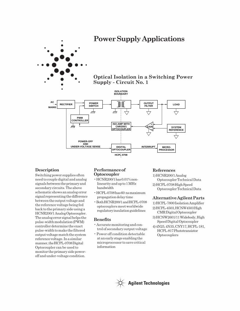
Power Supply Applications
DescriptionSwitching power supplies often
need to couple digital and analog
signals between the primary and
secondary circuits. The above
schematic shows an analog error
signal representing the difference
between the output voltage and
the reference voltage being fed
back to the primary side using a
HCNR200/1 Analog Optocoupler.
The analog error signal helps the
pulse-width modulation (PWM)
controller determine the exact
pulse-width to make the filtered
output voltage match the system
reference voltage. In a similar
manner, the HCPL-0708 Digital
Optocoupler can be used to
monitor the primary side power-
off and under-voltage condition.
Performance ofOptocoupler• HCNR200/1 has 0.01% non-
linearity and up to 1 MHz
bandwidth
• HCPL-0708 has 60Cns maximum
propagation delay time
• Both HCNR200/1 and HCPL-0708
optocouplers meet worldwide
regulatory insulation guidelines
Benefits• Accurate monitoring and con-
trol of secondary output voltage
• Power off condition detectable
at an early stage enabling the
microprocessor to save critical
information
References1) HCNR200/1 Analog
Optocoupler Technical Data
2) HCPL-0708 High Speed
Optocoupler Technical Data
Alternative Agilent Parts1) HCPL-7800 Isolation Amplifier
2) HCPL-4503, HCNW4503 High
CMR Digital Optocoupler
3) HCNW2601/11 Widebody, High
Speed Digital Optocoupler
4) 4N25, 4N35, CNY17, HCPL-181,
HCPL-817 Phototransistor
Optocouplers
Optical Isolation in a Switching PowerSupply - Circuit No. 1
RECTIFIER POWERSWITCH
OUTPUTFILTER LOAD
ISO-AMP WITHCNR200/1
OPTOCOUPLER
DIGITALOPTOCOUPLER
PWMCONTROLLER
SYSTEMREFERENCE
MICRO-PROCESSOR
AC
MAINS
ISOLATIONBOUNDARY
INTERRUPT
GAIN
POWER-OFFAND
UNDER-VOLTAGE SENSE
HCPL-0708
+
—

74
Optical Isolation in a Switching Power Supply -Circuit No. 2
Description
The above figure shows a push-
pull switching power supply that
utilizes the HCPL-2200
optocoupler to drive switching
transistors. The above circuit
uses a silicon unilateral switch
(SUS) to bootstrap start the
power supply when power is first
applied. The inhibit function in
the HCPL-2200 optocoupler has
been used to good advantage to
provide a common-mode conduc-
tion interlock function that will
not allow both the switching
transistors to turn on at the same
time.
Performance ofOptocoupler
• Maximum propagation delay:
300 ns
• Input turn-on current: 1.6 mA
• Common-mode transient
rejection: 1000 V/µs
Benefits• The power switches are
protected from common-mode
conduction failures caused by
EMI
• Regulation range is increased
since no deadtime is required
• Design is tolerant to propaga-
tion delay changes due to lot-to-
lot component variations
References
HCPL-2200 High CMR
Optocoupler Technical Data
Alternative Agilent Parts1) HCPL-2219 Very High CMR
Optocoupler
2) HCNW2601/11 Widebody High
CMR Optocoupler
ACPOWER
PWM CHIP
L
N
5 V+
HCPL-2200
5 V
+
HCPL-2200
+
ISOLATEDDCOUTPUT
SUS*CATHODE
ANODE
* SUS = SILICON UNILATERAL SWITCH
D1 R3
C1 R4
R1
C2
R2
R7
R9
D2
C3
C4
D3
R5
R6
R8
R11
R12
R10
C8
C6 C7
L1
D5
D4
R13

75
Optical Isolation in a DC/DC Converter
The HCPL-0708 high speed
optocoupler provides very good
safety isolation between primary
and secondary sections of the
DC/DC converter as shown in the
above figure. The switching
frequency specification of the
DC/DC converter is met by the
low propagation delay (60Cns
max.) and 15Cns typical pulse
width distortion of HCPL-0708
CMOS compatible high speed
optocoupler. The smaller size,
better noise immunity
performance, high reliability and
wide operating temperature make
HCPL-0708 ideally suited for such
applications.
Performance ofOptocoupler• HCPL-0708: 60Cns maximum
propagation delay time and
15Cns typical pulse width
distortion
• 10KV/µs minimum CMR @ Vcm
= 1KV
• Wide operating temperature:
-40 to 100°C
Benefits• Accurate monitoring and
control of output voltage
• Low propagation delay
• Small size and high reliability
• CMOS compatible and easy
interface
Description Alternative Agilent Parts1) HCPL-0600 High Speed
Optocoupler
2) HCPL-2200 High CMR
Optocoupler
3) 4N25, 4N35, CNY17, HCPL-181,
HCPL-817 Phototransistor
Optocouplers
Isolation Boundary
Power SwitchDC Input
Digital OptocouplerHCPL-0708 PWM Controller
Synchronous Rectifier/
Output FilterLoad
IsolatedBias Supply

The following application notes and technical articles are available on
Agilent Technologies’ web site at
http://www.agilent.com/view/optocouplers
They can also be obtained from your local Agilent Technologies' sales
office or authorized Agilent distributor.
Application Notes• AN 1004
Threshold Sensing for Industrial Control Systems with the
HCPL-3700 Interface Optocoupler
• AN 1018
Designing with the HCPL-4100 and HCPL-4200 Current Loop
Optocouplers
• AN 1023 (Pub. 3/85)
Radiation Immunity of Agilent Technologies Optocouplers
• AN 1024 (Pub. 3/85)
Ring Detection with the HCPL-3700 Optocouplers
• AN 1043 (Pub. 2/97)
Common-Mode Noise: Sources and Solutions
• AN 1046 (Pub. 11/96)
Low On-Resistance Solid State Relays
• AN 1059 (Pub. 2/93)
High CMR Isolation Amplifier for Current Sensing Applications
• AN 1063 (Pub. 7/93)
A Designer’s Guide to HCPL-7600 Series, Low Input-Current,
High Speed Optocouplers
• AN 1074 (Pub. 11/96)
Optocoupler Input-Output Endurance Voltage
• AN 1078 (Pub. 11/96)
Designing with Agilent Technologies Isolation Amplifiers
• AN 1087 (Pub. 11/96)
Thermal Data for Optocouplers
• AN 1252
Variable Speed Drive Applications in the Consumer Market
• AN 1253
Variable Speed Drive Applications in the High-power
Industrial:Market
Application Notes

77
• AN 1254
Variable Speed Drive Applications in the Low-power
Industrial:Market
• AN 951-1
Applications for Low Input Current, High Gain Optocouplers
• AN 951-2
Linear Applications of Optocouplers
• SN 101
Overview of Agilent Technologies Optical Isolation Technology and Products for
Motor Control Applications
Application Notes, continued

www.agilent.com/semiconductorsFor product information and a complete list ofdistributors, please go to our web site.
For technical assistance call:Americas/Canada: +1 (800) 235-0312 or(408) 654-8675
Europe: +49 (0) 6441 92460
China: 10800 650 0017
Hong Kong: (+65) 6271 2451
India, Australia, New Zealand: (+65) 6271 2394
Japan: (+81 3) 3335-8152(Domestic/International), or0120-61-1280(Domestic Only)
Korea: (+65) 6271 2194
Malaysia, Singapore: (+65) 6271 2054
Taiwan: (+65) 6271 2654
Data subject to change.Copyright © 2002 Agilent Technologies, Inc.Obsoletes 5968-4800EJune 7, 20025988-4082EN