A cryogen-free HTS Josephson junction detector for ... · A cryogen-free HTS Josephson junction...
16
1 A cryogen-free HTS Josephson junction detector for terahertz imaging J. Du (1) , K. Smart (1) , L. Li (1) , K. E. Leslie (1) , S. M. Hanham (2) , D. H. C. Wang (1) , C. P. Foley (1) , F. Ji (3) , X. D. Li (3) , and D. Z. Zeng (3) (1) Commonwealth Scientific and Industrial Research Organisation (CSIRO), Lindfield, NSW 2070, Australia (2) Dept. of Materials, Imperial College, London, U.K. (3) Chengdu Shuguang Optical Fiber Network Co., Ltd, Chengdu, Sichuan, China Abstract A cryogen-free terahertz (THz) imaging system based on a high-temperature superconducting (HTS) Josephson junction detector is reported. The detector was made of a YBa 2 Cu 3 O 7-x (YBCO) step-edge Josephson junction and integrated into an on-chip thin-film antenna. The HTS Josephson detector was cooled via a commercial mechanical cryocooler; an important step towards cryogen-free THz instrumentation, which is critical for industrial acceptance. In addition, it is shown that operating the detector in a cryocooler provides improved flexibility for optimising the detector parameters and performance due to the ability to adjust the temperature compared to liquid nitrogen cooling methods. The DC and AC characteristics, the detector responsivity and the noise-equivalent power (NEP) of the detector, and resulting image quality were studied as the function of operating temperatures. Introduction Terahertz (THz) radiation lies in the frequency gap between the microwave and infrared (IR) regions of the electromagnetic spectrum and displays many unique properties such as strong sensitivity to water, high transmission through a range of non-conducting materials and spectroscopic responses to materials [1, 2]. These features mean THz technology holds significant potential in the areas of security screening (detection of explosives, drugs, hidden weapons and other objects), material characterisation, non-destructive testing, medical imaging, chemical sensing and food and agricultural product inspection (see, for example, review papers [1-4]). THz radiation is non-ionising and is therefore safer for humans compared to X-ray based imaging. Despite huge potential, the up- take of THz technology has been slow mainly due to limitations of available source and detector
Transcript of A cryogen-free HTS Josephson junction detector for ... · A cryogen-free HTS Josephson junction...

1
A cryogen-free HTS Josephson junction detector for terahertz imaging
J. Du(1), K. Smart(1), L. Li(1), K. E. Leslie(1), S. M. Hanham(2), D. H. C. Wang(1), C. P. Foley(1), F. Ji(3), X. D. Li(3),
and D. Z. Zeng(3)
(1) Commonwealth Scientific and Industrial Research Organisation (CSIRO), Lindfield, NSW 2070,
Australia
(2) Dept. of Materials, Imperial College, London, U.K.
(3) Chengdu Shuguang Optical Fiber Network Co., Ltd, Chengdu, Sichuan, China
Abstract
A cryogen-free terahertz (THz) imaging system based on a high-temperature superconducting (HTS)
Josephson junction detector is reported. The detector was made of a YBa2Cu3O7-x (YBCO) step-edge
Josephson junction and integrated into an on-chip thin-film antenna. The HTS Josephson detector
was cooled via a commercial mechanical cryocooler; an important step towards cryogen-free THz
instrumentation, which is critical for industrial acceptance. In addition, it is shown that operating the
detector in a cryocooler provides improved flexibility for optimising the detector parameters and
performance due to the ability to adjust the temperature compared to liquid nitrogen cooling
methods. The DC and AC characteristics, the detector responsivity and the noise-equivalent power
(NEP) of the detector, and resulting image quality were studied as the function of operating
temperatures.
Introduction
Terahertz (THz) radiation lies in the frequency gap between the microwave and infrared (IR) regions
of the electromagnetic spectrum and displays many unique properties such as strong sensitivity to
water, high transmission through a range of non-conducting materials and spectroscopic responses
to materials [1, 2]. These features mean THz technology holds significant potential in the areas of
security screening (detection of explosives, drugs, hidden weapons and other objects), material
characterisation, non-destructive testing, medical imaging, chemical sensing and food and
agricultural product inspection (see, for example, review papers [1-4]). THz radiation is non-ionising
and is therefore safer for humans compared to X-ray based imaging. Despite huge potential, the up-
take of THz technology has been slow mainly due to limitations of available source and detector
2
technologies. In recent years, THz science and technology has become an intensely researched field
around the world and major progress has been made in developing new THz sources, detectors,
imaging and spectroscopy systems using a range of technologies.
Superconducting devices offer a viable option as they are excellent generators and detectors of
terahertz radiation. Superconducting THz emitters [5, 6] and sensors [7-12] have been reported. We
have, in recent years, developed high-Tc superconducting (HTS) Josephson THz detectors and
demonstrated their use for THz imaging [10-12]. HTS devices offer not only the obvious advantage of
higher operating temperatures compared to their low-Tc superconducting (LTS) counterpart, but also
a very high band-gap voltage which extends their response well into the THz range. In previous work,
the HTS detectors were operated in liquid helium [9] or liquid nitrogen [10, 11]. In this work, we
have developed a terahertz imaging system based on a HTS Josephson detector operating in a
commercial cryocooler. A cryogen-free system is an essential step towards industrial acceptance.
Compared to LTS detectors, HTS detectors can operate using a relatively inexpensive and more
compact single-stage cryocooler. Furthermore, the controllable temperature of a cryocooler allows
for the optimisation of the detector parameters to achieve improved performance. This work also
differs from our previous system in that we have integrated a more compact solid-state THz source
and redesigned the thin-film antenna-coupled HTS detectors. We shall show that THz images of high-
visual quality were obtained with this configuration. The full characterisations of the detectors
operating in the cryocooler and the acquired THz image quality at different temperatures are
described in this paper.
Experimental Details
About the detectors
The terahertz detectors consist of a HTS step-edge Josephson junction integrated across the slot of a
ring-slot antenna which was designed with a centre frequency of 600 GHz and ~ 12% bandwidth,
shown in Fig. 1c. In operation, an incident THz wave (RF signal) excites currents on the antenna
which pass through the junction; the RF signal is detected via changes in the junction’s electrical
characteristics. A more detailed description of the operating principle of this type of detector can be
found in reference [11].
The HTS detectors were fabricated on MgO substrates using the CSIRO HTS step-edge junction
technology [13, 14]. Briefly, the MgO substrates were photo-lithographically patterned and etched
using Ar-ion beam milling to produce steps of ∼400 nm in height with an angle of ∼35 to the
substrate surface. S-type (smooth film morphology) YBCO films of 220 nm thickness and a 50 nm in

3
situ gold film were deposited by Ceraco GmbH, Germany. The YBCO film is patterned and ion-beam
etched to form a 2 μm wide Josephson junction. The in situ Au was removed from the junction area
using the in-housing Ar reactive ion etching technique. An additional gold layer of ~ 300 nm thick
was then deposited and patterned to form the antenna structure and contact pads. An in situ Au
layer is necessary to improve the adhesion of the Au layer to YBCO film and reduce the contact
resistance [15]. However, our study also showed if using YBCO film and Au bi-layer for the antenna,
the noise increased presumably due to both increased surface resistance of YBCO film at high
frequency and large contact resistance between the YBCO and Au films. We have, therefore, used Au
thin-film for the antenna and kept only narrow YBCO micro strip lines for the DC current and voltage
leads (see Fig. 1 (c) and (d)).
Figure 1 shows a micrograph of the fabricated chip containing a 2 x 2 array of gold thin-film antenna-
coupled to YBCO Josephson junction detectors. The antennas are positioned on the centre of the
substrate so that they are at the focal spot of a 6 mm diameter high resistivity silicon lens which is
bonded to the reverse side of the substrate. The combination of the MgO substrate and
hemispherical silicon lens forms a hyper-hemispherical lens which ensures a high antenna directivity
and efficient coupling between free-space and the antennas. The arcs visible in Fig. 1a denote the
extent of the lens and were used to align the lens to the antennas.
The design of the antenna-coupled detector is different from those reported in [10, 11] where the
junction was located across the ring slot but at a position orthogonal to the axis of the coplanar
waveguide filter. The step-edge junctions reported here are integrated across the ring slot at a
position which is co-linear with the coplanar waveguide filter and the local slot width has two
different sizes: 4 µm and 7 m for optimising the RF coupling. The slot width is widened at the
junction for easier junction alignment in the ring slot during device fabrication. These modifications
were undertaken to improve the impedance matching between the ring slot antenna and the
junction. The very low impedance (typically, 1-5 ) of the junction makes impedance matching
difficult and care must be taken when designing the device to avoid shorting the ring slot antenna
with the junction which would have a deleterious effect on the antenna’s performance.

4
Figure 1: Micrographs of the fabricated device chip containing four antenna-coupled HTS Josephson detectors
at magnifications (a) 100x, (b) 200x, (c) 500x and (d) 1000x. (d) shows a 2 μm wide YBCO electrode (black
colour) is patterned across the antenna slot connecting the inner and outer conductors of the antenna and
across a step-edge on the MgO substrate inside the slot forming a step-edge junction.
The detector/antenna/lens was then mounted on a commercial pulse-tube cryocooler (PTC) (Janis
model PTSHI-4-5 by Research Inc.) cold-head with the silicon lens on the back of the chip facing the
cryocooler window where the THz beam radiation is incident, as shown in Fig. 2. The detector
characteristics and acquisition of the THz images were studied over the operating temperature
range 50 K to 77K; a temperature range attainable with a single stage miniature cryocooler. It should
be noted that a significantly smaller cryocooler than the one used here could be employed in future
systems to improve system portability.
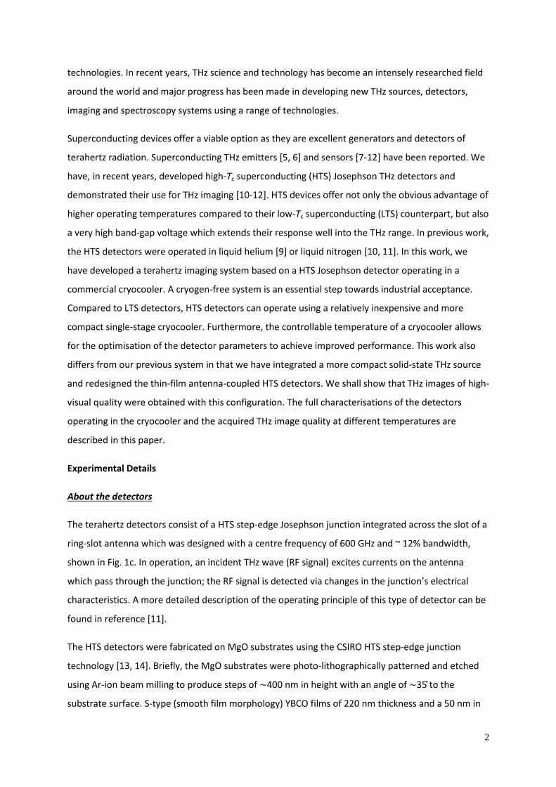
The THz imaging system
Figure 2 shows a photograph of the THz imaging system integrated with the PTC cooler. It is an
active transmission imaging scheme, i.e., the object being imaged is illuminated by a continuous-
wave THz source and the THz wave transmitted through the object is detected. A more compact
commercial solid-state THz source (VDI 625 GHz Amplifier Multiplier Chain (AMC)) with a small
(a) (b)
(c) (d)
5
economy frequency synthesizer as the RF input signal was used to replace the bulky back-wave-
oscillator (BWO) THz source used in previous experiments [10-12] for a more compact simpler
electronic imaging system. The THz signal was transmitted via a quasi-optical scheme with two pairs
of collimating and focusing mirrors onto the sample and then to the detector in the cryocooler. The
cold stage was connected to the compressor via semi-rigid flexible gas cables clad with vibration
damping materials. No -metal or other low-frequency magnetic shields were used around the
sample stage. The HTS Josephson detector operated stably without observable performance
degradation (see later section for noise characterisation). The sample being imaged is raster scanned
in a plane perpendicular to the beam axis using a linear XY motor stage. The theoretical spatial
resolution can be estimated using the Rayleigh criterion ∆x = 1.22 f/D assuming the perfect optical
alignment, where the wavelength = 3x10⁸ms-1/614GHz = 488 m, f and D are focal length and
diameter of the focusing mirror. The estimated theoretical spatial resolution is 1.19 mm. In the
experiments, we scanned the sample at a typical resolution of 0.5 mm. An area of 5 cm x 5 cm, i.e.
an image size of 100 x 100 or 10,000 pixels took about 10 minutes to complete.
The Josephson junction was current biased above its critical current Ic at the point on the DC current-
voltage characteristic (IVCs), where the dynamic resistance, Rd = dV/dI, is the maximum. The voltage
response, VRF, induced by the chopper-modulated THz power was amplified 100 times using a low
noise integrated circuit (Burr Brown type INA 103) at room temperature. A lock-in amplifier
synchronized to the 1 kHz optical chopper wheel signal was used to acquire the voltage response,
which was processed using an in-house developed Labview software program to produce an image.
The software PicoScope was used to capture the DC IVCs and the real-time voltage response traces.
A HP 35670A dynamic signal analyser was used to record the detector noise spectra.
Chopper
AMC THz source
Detector in PTC
AMC THz source
AMC THz source
Sample
AMC THz source
XY linear stage

6
Figure 2: Photograph of the transmission THz imaging system: a solid-state THz source on the front, an optical
chopper, a sample driven by a motorised XY-linear stage, and the antenna-coupled HTS detector mounted on
the cold-head facing the window on a commercial PTC cooler on the back.
Results and discussion
Detector Characterisations
Figure 3 shows the IVCs of a detector at different operating temperatures. The junction
demonstrated a resistively-shunted-junction like behaviour with a normal resistance of Rn ≈ 1.5 Ω.
The junction critical current, Ic, increased with decreasing temperature, from ~ 80 µA at 77 K to 827
µA at 50 K. The junction characteristic voltage, Vc ≡ IcRn, versus the temperature is plotted in the
inset. The IcRn value increases from ~ 120 V at 77 K to ~ 1.24 mV at 50 K, which corresponds to a
characteristic frequency, fc ≡ IcRn/0 (where 0 is the magnetic flux quantum, 1/0 ≡ 2e/h =
0.4836 GHz/V) of ~ 60 GHz at 77 K to ~ 600 GHz at 50 K. By varying the temperature, the Vc and fc
values can be adjusted to optimise the detector performance or achieve broadband frequency
detection, demonstrating the advantage of using a temperature-adjustable cryocooler.
Figure 4 (a) shows the IVCs at 70 K under THz signal radiation at different power levels. The variation
of the power level was achieved by inserting layers of cardboard (CB) of which each layer was
measured to exhibit 3dB of attenuation. The THz signal suppresses the Ic value and induces Shapiro
steps at voltages Vn = n0fs = n × (1.27 mV) (n = …, -2, -1, 0, 1, 2, …), where the signal frequency fs =
614.2 GHz. The relationship of the junction critical Ic value and the 1st Shapiro step height versus the
THz signal power are plotted out in Fig. 4(b). The Ic decreases and first Shapiro current step increases
with increasing the THz signal power as predicted. By measuring the current step heights, we could
estimate the THz power coupled into the junction using the Bessel functions (in approximation):
Ic/Ic0 = J0 (2eVs/hf) or ∆In=1 = J1 (2eVs/hf), where the J0 and J1 are 0 and 1-order Bessel functions, Ic0 is
the junction critical current without THz radiation, and Ps = ½ Vs2/Rn or = ½ Is
2Rn is the RF signal
power coupled into the junction. The THz power coupled into the junction was estimated to be in
the range of sub micro watts to several micro watts.

7
Figure 3: DC IVCs at different temperatures; inset shows the relationship of IcRn product versus T (k).
-2500 -2000 -1500 -1000 -500 0 500 1000 1500 2000 2500
-1500
-1000
-500
0
500
1000
1500
50 55 60 65 70 75 800
200
400
600
800
1000
1200
1400
I cR
n (V
)
T (K)
IcR
n
I
(A
)
V (V)
77K
70K
60K
50K
77K

8
Figure 4 (a) The IVCs at 70 K versus applied THz signal power; (b) shows the relationship of the junction critical
Ic value and the current height of the 1st
Shapiro step versus with the THz signal power changes (the lines
through the symbols are guide to the eye).
0 5 10 15 20 25
0
20
40
60
80
100
120
140
160
180
200
220(b) I
c
In=1
I (
A)
Ps (dB)
-2500-2000-1500-1000 -500 0 500 1000 1500 2000 2500-1500
-1000
-500
0
500
1000
1500
Ic ~ 210 A
1.27 mVx 0.4836 GHz/V = 614.2 GHz
I (
A)
V (V)
THz blocked
THz on, 4 CBs
THz on, 3 CBs
THz on, 2 CBs
THz on, 1 CBs
THz on, no CBs
Ps increases
Rn ~ 1.5
(a)

9
Figure 5: The measured voltage response VRF versus the bias current IB at 70 K. The maximum output voltage
occurs at the point just above the THz signal suppressed Ic.
When the Josephson junction is current biased above its critical current, Ic0, on the I-V curve and a
chopper-modulated THz wave is incident, a RF voltage response, VRF, is induced across the junction.
The voltage response VRF amplitude is bias-current dependent. Fig. 5 shows the measured voltage
response VRF versus the bias current IB at 70 K. The voltage output changes with the bias position and
reaches a maximum at the point just above the THz signal-suppressed Ic.
We have measured the antenna-coupled detector RF voltage response versus the signal frequency.
The obtained frequency response range is from 590 GHz to 650 GHz, i.e. ~ 10% bandwidth. However,
we also measured the radiation frequency pattern of the AMC source using the VDI diode, which
showed the similar frequency pattern. Therefore, we conclude that the simulated bandwidth (~ 12%)
of the ring slot is larger than the source frequency bandwidth (~ 10%) and it was not possible for us
to experimentally verify the radiation pattern bandwidth of the ring-slot antenna.
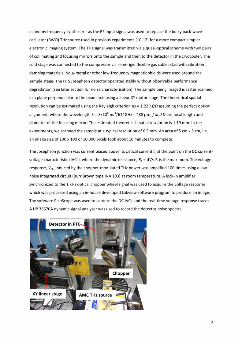
Figure 6 shows the acquired real-time voltage response VRF (t) to the chopped THz beam at different
operating temperatures. The amplitude of the detector response increases significantly with
decreasing the temperature. This is because the dynamic resistance RD (V) = dV/dI increases with
0 100 200 300 400
0
2
4
6
8
10
V
RF (
mv)
IB (A)
10
decreasing temperature and therefore the voltage response VRF = RD∆I increases, where ∆I is the THz
induced current change amplitude. The maximum amplitude of voltage response at 50 K is 122 mV
and the noise floor on the lock-in amplifier was ∼1 μV (after x100 amplification), giving a signal-to-
noise ratio (SNR) in an order of ~ 1X10⁵ or 100 dB, which is further improvement from previously
achieved SNR of 45 dB [11]. The voltage response amplitude decreases with increasing temperature
reducing to VRF ≈ 5.7 mV and SNR ~ 5x10³ at 77 K.
Figure 6: Measured real-time detector voltage signal at the 100x LNA output at different temperatures (DC
offset has been added to some of the traces to improve clarity).
The voltage output for a given input RF signal will depend on the responsivity of the maximum zero-
voltage current to RF signal. The greater the dynamic resistance, RD = dV/dI, at the operating point,
the greater the output voltage will be. We can estimate the detector voltage responsivity using the
following simple expression if we assume the load circuit is matched to the dynamic resistance, RD,
of the junction and the input impedance to be simply the junction resistance Rn [16].
The voltage responsivity can be expressed as:
= VRF/Ps = 2VRF/Is2Rn = RD/(2Ic0Rn
2), (1)
0 1 2 3 4 5 6-20
-10
0
10
20
30
40
50
60
70
80
90
100
110
120
130
140
THz blocked
77K
70K
60K
VR
F (
mV
)
Time (ms)
50K

11
where Ps = (1/2)Vs2 /Rn or (1/2)Is
2Rn is the RF signal power coupled into the junction (Is and Vs are the
RF signal current and voltage amplitude respectively), which induces the voltage output VRF. is the
normalised frequency, = fs/fc = fs/(Ic0Rn x 2e/h) and 1/0 = 2e/h = 0.4836 GHz/V. Here 1 when
the detector operates in the range of 77 K to 50 K. It can be seen from equation (1) that the
responsivity is inversely proportional to 2 (or fs2), i.e., lower frequency and/or higher IcRn value
raise the sensitivity. The RD value can be obtained by differentiating the measured detector IVCs and
the maximum RD value was used to estimate the responsivity. Figure 7 shows the responsivity
against the operating temperature and the IcRn value. The responsivity increases significantly with
decreasing temperature (thus increasing IcRn value) from 77 K to 50 K, where the responsivity ≈
7000 V/W at 50 K. This shows that operating the HTS Josephson detector in a cryocooler has the
advantage of improving the detector performance significantly by adjusting the temperature
compared to using liquid nitrogen (77 K). 50 K can be readily achieved using a single-stage miniature
cryocooler. The achieved responsivity at 50 K is about an order of magnitude better than a
commercial semiconductor diode detector in the same frequency band (for example, 750 V/W for a
VDI zero biased detector at 500-750 GHz [17]).
Figure 7: The detector voltage responsivity versus operating temperature and IcRn value.
45 50 55 60 65 70 75 80
0
1000
2000
3000
4000
5000
6000
7000
80001400 1200 1000 800 600 400 200 0
Re
sp
on
siv
ity (
V/W
)
T (K)
IcR
n (V)

12
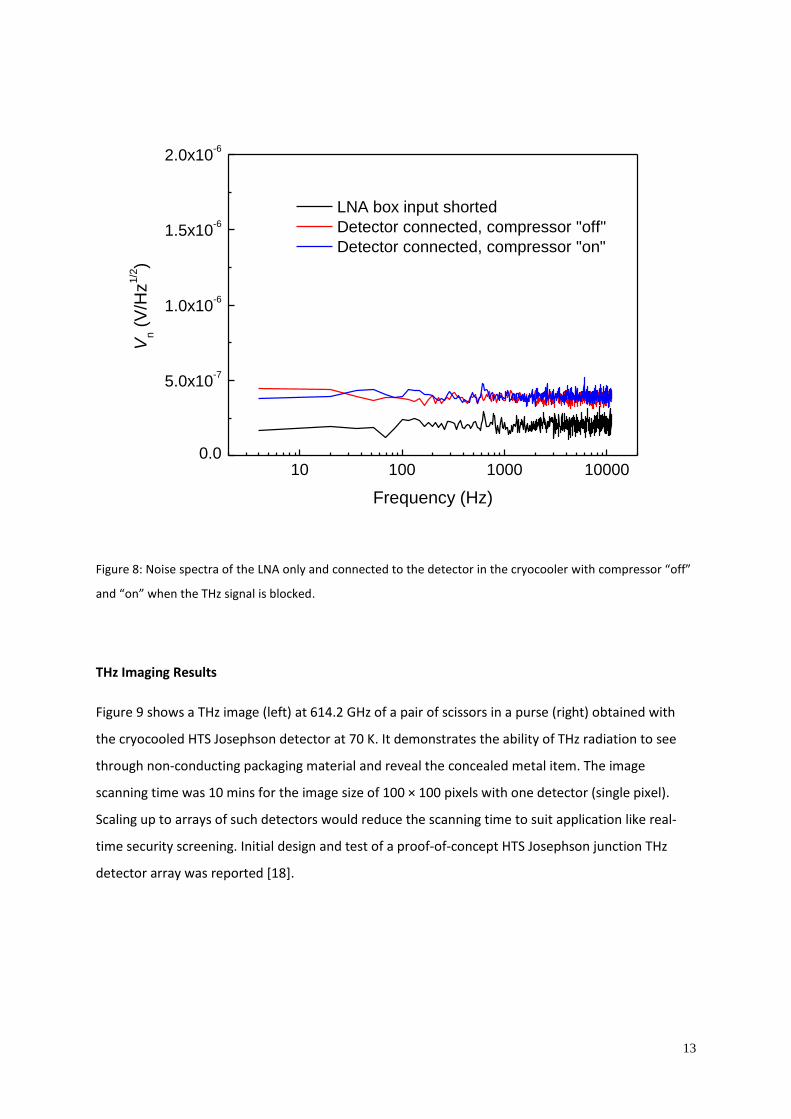
We also measured the noise performance of the Josephson detectors. Figure 8 shows the noise
spectra of the low-noise amplifier (LNA), detector base-noise with cryocooler compressor “off” and
“on” when the THz signal is blocked. The measured LNA input noise when shorted at input is 2
nV/√Hz. When the detector is connected to the LNA, the input noise is 3-4 nV/√Hz of which the
slight increase is believed to be due to the long wires from the detector to the LNA. There were
negligible changes the noise floor when the PTC compressor turned “on” and “off” indicating that
the cryocooler contributes little noise to the detector noise. The detector noise was limited by the
room temperature LNA rather than the HTS Josephson junction intrinsic noise. We can estimate the
noise equivalent power (NEP) of the detector using the input noise of the LNA and the measured
voltage responsivity of the detector. A NEP of ~ 3x10-13 W/√Hz to 5 x10-12 W/√Hz was obtained for
the detector operating at 50 K to 77 K, an order of magnitude improvement when the operating
temperature lowered from 77 K to 50 K. It is anticipated that the sensitivity and the NEP should
continue to improve with further decreasing the temperature. However, our HTS detectors were
designed for operating at higher temperatures and 50-77K is the typical temperature range a single-
stage cryocooler could reach. It is worth mentioning that the estimated NEP = 1.67x10⁻¹¹ W/√Hz of
our earlier detector working at 10 K reported in [10] was for the imaging system noise rather than
for the HTS Josephson detector as it was amplified 100x and included the lock-in amplifier noise.
Using the pre-amplified noise figure, i.e., 1V/100 = 10 nV, a NEP of ~ 1.67 x10⁻¹³W/√Hz was btained
for the detector reported in [10].
13
Figure 8: Noise spectra of the LNA only and connected to the detector in the cryocooler with compressor “off”
and “on” when the THz signal is blocked.
THz Imaging Results
Figure 9 shows a THz image (left) at 614.2 GHz of a pair of scissors in a purse (right) obtained with
the cryocooled HTS Josephson detector at 70 K. It demonstrates the ability of THz radiation to see
through non-conducting packaging material and reveal the concealed metal item. The image
scanning time was 10 mins for the image size of 100 × 100 pixels with one detector (single pixel).
Scaling up to arrays of such detectors would reduce the scanning time to suit application like real-
time security screening. Initial design and test of a proof-of-concept HTS Josephson junction THz
detector array was reported [18].
10 100 1000 100000.0
5.0x10⁻⁷
1.0x10⁻⁶
1.5x10⁻⁶
2.0x10⁻⁶
V
n (
V/H
z1/2)
Frequency (Hz)
LNA box input shorted
Detector connected, compressor "off"
Detector connected, compressor "on"

14
Figure 9: A THz image (left) of a pair of scissors in a purse (right) obtained with the cryocooled HTS Josephson
detector at 70 K.
Figure 10 shows a THz transmission image of a leaf obtained by the cryocooled HTS detector
operating at 77 K and 60 K. The imaging resolutions and times (10 mins) for Figs. 10 (b) and (c) were
identical. The image highlights one of the key THz features, i.e., the sensitivity to water with the
higher water content in the leaf veins exhibiting higher attenuation. The 77 K image is noisier than
that of the 60 K image. The 60 K image shows very clear details of the small variations in the leaf’s
thickness and minor vein details as a result of a higher SNR.
(a) (b) (c)
Figure 10: The photograph (a) and THz images of a leaf obtained with the Josephson detector operating at 60 K
(b) and 77 K (c).
Conclusions:
A cryogen-free HTS Josephson detector-based terahertz imager was presented. A compact,
simplified solid-state device based quasi-optic THz imaging system at 600 GHz band was
demonstrated and high-quality THz images were obtained. The DC and AC characteristics of the thin-
film antenna-coupled HTS step-edge junction detector were studied against the operating

15
temperatures from 50 K to 77 K, a temperature range attainable with a relatively cheap more
compact single stage cryocooler. The detector responsivity, SNR and NEP improved dramatically with
decreasing temperature; a sensitivity of ~ 7000 V/W, SNR ~ 1x10⁵ and a NEP ≈ 3 x10-13 W/√ Hz were
obtained at 50 K. The quality of the acquired images improves significantly with decreasing
temperature due to improved responsivity and SNR, a clear advantage of using a cryocooler rather
than liquid nitrogen for cooling. The results clearly demonstrated the potential of terahertz imaging
using a cryogen-free HTS Josephson junction detector, an important step for gaining industry
acceptance of this technology.
ACKNOWLEDGMENT
Earlier contributions from Drs Andrew Hellicar, Nasiha Nikolic, John Macfarlane, and the HTS chip
fabrication by Jeina Lazar of CSIRO are gratefully acknowledged.
References:
1. Tonouchi M 2007 Cutting-edge terahertz technology, Nature Photonics 1, 97-105.
2. Jansen C, et al. 2010 Terahertz imaging: applications and perspectives, Applied Optics. 49 (19),
E48.
3. Chan W L, Deibel J, and Mittleman D M 2007 Imaging with terahertz radiation, Rep. Prog. Phys.
70 1325-1379.
4. Mathanker S K, Weckler P R and Wang N 2013 Terahertz (THz) applications in food and
agriculture: a review, Transactions of the ASABE. 56 (3) 1213-1226.
5. Ozyuzer, L, et al. 2007 Emission of coherent THz radiation from superconductors, Science 318,
1291-1293.
6. Wang H B, et al. 2010 Coherent terahertz emission of intrinsic Josephson junction stacks in the
hot spot regime, Phys. Rev. Lett. 105 057002.
7. Ariyoshi S, Otani C, Dobroiu A, Sato H, Kawase K, Shimizu H M, Taino T, and Matsuo H 2006
Terahertz imaging with a direct detector based on superconducting tunnel junctions Appl. Phys.
Lett. 88 203503.
8. Luukanena A, Gronberg L, Helisto P, Penttila J S, Seppa H, Sipola H, Dietlein C R and Grossman E
N 2006 An array of antenna-coupled superconducting microbolometers for passive indoors real-
time THz imaging Proc. of SPIE 6212 62120Y-2.
9. Chen J, Kurigata Y, Wang H B, Nakajima K, Yamashita T and Wu P H 2003 Wideband frequency
metrology using high temperature superconducting Josephson junctions IEEE Trans. Appl.
Supercond. 13 1143-1146.
16
10. Du J, Hellicar A D, Li L, Hanham S M, Nikolic N, Macfarlane J C and Leslie K E 2008 Terahertz
imaging using a high-Tc superconducting Josephson junction detector Supercond. Sci. Technol. 21
125025.
11. Du J, Hellicar A D, Li L, Hanham S, Macfarlane J C, Leslie K E, Nikolic N, Foley C P, and Greene K J
2009 Terahertz imaging at 77 K Supercond. Sci. Technol. 22 114001.
12. Du J, Hellicar A D, Hanham S, Li L, Macfarlane J C, Leslie K E and Foley C P 2011 Terahertz and
millimetre wave imaging with a broadband Josephson detector working above 77 K J Infrared,
Millimeter, and Terahertz Waves 32 681–690.
13. Foley C P, Mitchell E E, Lam S K H, Sankrithyan B, Wilson Y M, Tilbrook D L, and Morris S J 1999
Fabrication and characterisation of YBCO single grain boundary step edge junctions IEEE Trans.
Appl. Supercond. 9 4281-4284.
14. Mitchell E E and Foley C P 2010 YBCO Step-edge junctions with high IcRn Supercond. Sci. Technol
23 065007.
15. Du J, Lam S K H, and Tilbrook D L 2001 Metallization and interconnection of HTS YBCO thin
film devices and circuits, Supercon. Sci. & Technol 14 820-825.
16. Van Duzer T and Turner C W 1999 Superconductive Devices and Circuits, 2nd edition, Prentice-
Hall, Inc, New Jersey, USA.
17. Hesler J L and Crowe T W 2007 NEP and responsivity of THz zero-bias Schottky diode detectors,
the 15th Intern. Conf. on Terahertz Electronics IRMMW-THz, September 2007 pp 844–5. Also see
website: http://vadiodes.com VDI detectors datasheet.
18. Du J, Hellicar A D, Leslie K E, Nikolic N, Hanham S, Macfarlane J C, Foley C P 2013 Towards
Large Scale HTS Josephson Detector Arrays for THz Imaging, Supercond. Sci & Technol. 26
115012.