A Clock and Data Recovery Circuit with a Novel Multi-Level ...
135
A Clock and Data Recovery Circuit with a Novel Multi-Level Bang-Bang Phase Detector Structure Young-Seok Park The Graduate School Yonsei University Department of Electrical and Electronic Engineering
Transcript of A Clock and Data Recovery Circuit with a Novel Multi-Level ...

A Clock and Data Recovery Circuit with a
Novel Multi-Level Bang-Bang Phase
Detector Structure
Young-Seok Park
The Graduate School
Yonsei University
Department of Electrical and Electronic Engineering

A Clock and Data Recovery Circuit with a
Novel Multi-Level Bang-Bang Phase
Detector Structure
A Dissertation
Submitted to the Department Electrical and Electronic Engineering
and the Graduate School of Yonsei University
in partial fulfillment of the requirements for the degree of
Doctor of Philosophy
Young-Seok Park
January 2014

This certifies that the dissertation of Young-Seok Park is approved.
Thesis Supervisor : Woo-Young Choi
Seong-Ook Jung
Young-Cheol Chae
Sung-Min Park
Pyung-Su Han
The Graduate School
Yonsei University
January 2014
Contents
List of Figures iv
List of Tables viii
Abstract ix
1 Introduction 1
1.1 High-Speed Serial Interface . . . . . . . . . . . . . . . . . . . . . . . . 1
1.2 Overview of The Phase Detector for CDR Application . . . . . . . . . 5
1.3 Outline of Dissertation . . . . . . . . . . . . . . . . . . . . . . . . . . 12
2 Backgrounds and Motivations 13
2.1 Loop Dynamics and Noise Analysis of CDR . . . . . . . . . . . . . . . 13
2.1.1 Linear PD . . . . . . . . . . . . . . . . . . . . . . . . . . . . . 13
2.1.2 BBPD . . . . . . . . . . . . . . . . . . . . . . . . . . . . . . . 19
2.1.3 Multi-Level BBPD . . . . . . . . . . . . . . . . . . . . . . . . 24
2.2 Performance Comparison Among Three Types of PDs . . . . . . . . . . 25
2.2.1 Environmental Sensitivity . . . . . . . . . . . . . . . . . . . . 25
i
2.2.2 Maximum Operating Speed and Power Consumption of CDRs . 31
3 CDR with a New Multi-Level BBPD 35
3.1 Time-Interleaved Multi-Level BBPD . . . . . . . . . . . . . . . . . . . 35
3.1.1 Operational Principle . . . . . . . . . . . . . . . . . . . . . . . 35
3.1.2 Implementation of Time-Interleaved BBPD . . . . . . . . . . . 40
3.1.3 The Gain of TI-BBPD . . . . . . . . . . . . . . . . . . . . . . 46
3.1.4 Input Jitter Sensitivity of TI-BBPD . . . . . . . . . . . . . . . 51
3.2 CDR with TI-BBPD . . . . . . . . . . . . . . . . . . . . . . . . . . . 57
3.2.1 Performance Simulation of TI-BBPD CDR . . . . . . . . . . . 57
3.2.2 Loop Bandwidth Control of TI-BBPD CDR . . . . . . . . . . . 64
3.2.3 The Spur Reduction Techniques for TI-BBPD CDR . . . . . . . 67
4 On-Chip Jitter Monitoring 72
4.1 The Necessity of Signal Monitoring . . . . . . . . . . . . . . . . . . . 72
4.2 Signal Monitoring Circuit for CDR . . . . . . . . . . . . . . . . . . . . 75
4.3 On-Chip Jitter Monitoring Circuit using TI-BBPD . . . . . . . . . . . . 79
5 Implementation 83
5.1 Overall Architecture . . . . . . . . . . . . . . . . . . . . . . . . . . . 83
5.2 TI-BBPD and CP . . . . . . . . . . . . . . . . . . . . . . . . . . . . . 83
5.3 Voltage-Controlled Oscillator . . . . . . . . . . . . . . . . . . . . . . . 89
5.4 Dead-Zone Width Controller . . . . . . . . . . . . . . . . . . . . . . . 93
5.5 Jitter Monitoring Circuit . . . . . . . . . . . . . . . . . . . . . . . . . 96
ii

6 Experimental Results 98
7 Summary 110
Appendix 113
A. Design and revision of printed circuit board . . . . . . . . . . . . . . . 113
iii

List of Figures
1.1 Block diagram of conventional I/O transceiver for serial interface . . . . 3
1.2 Block diagram of typical CDR . . . . . . . . . . . . . . . . . . . . . . 6
1.3 PD comparison (a) Hogge PD (b) Bang-Bang PD . . . . . . . . . . . . 7
1.4 (a) Characteristic of multi-level BBPD (b) Classical structure of multi-
level BBPD . . . . . . . . . . . . . . . . . . . . . . . . . . . . . . . . 10
2.1 Small signal model for CDR . . . . . . . . . . . . . . . . . . . . . . . 14
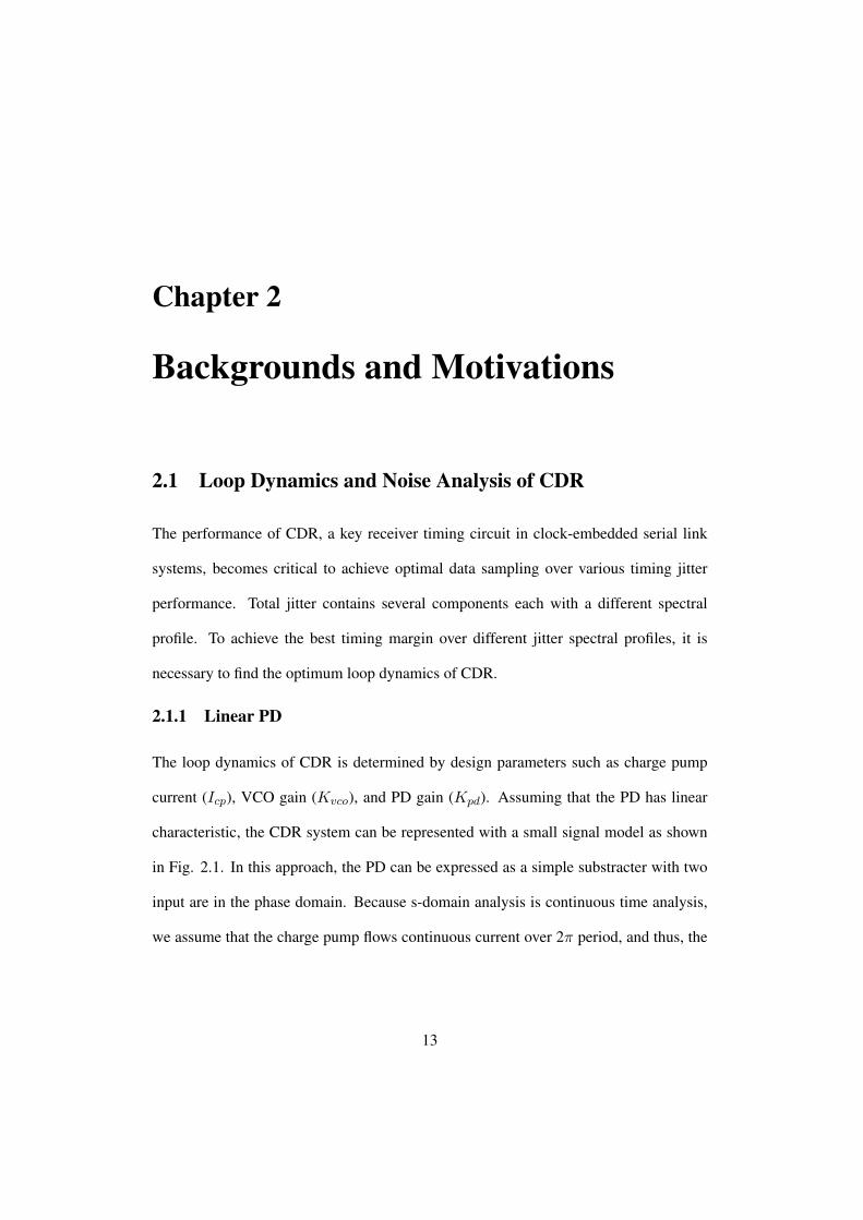
2.2 Small signal model for CDR with various noise sources . . . . . . . . . 15
2.3 Noise analysis of linear-CDR (a) Input data vs. φout (b) Icpn vs. φout (c)
Vcontn vs. φout (d) φV COn vs. φout . . . . . . . . . . . . . . . . . . . . 16
2.4 Recovered clock rms jitter vs. loop dyanmics setting . . . . . . . . . . 18
2.5 (a) BBPD output for a completely differential pair switching (b) BBPD
output for partial differential pair switching (c) BBPD output for incom-
plete regeneration (d) Typical BBPD characteristic. . . . . . . . . . . . 21
2.6 Smoothing of PD characteristic due to jitter . . . . . . . . . . . . . . . 23
2.7 Recovered clock rms jitter of 3 types of CDR under various loop filter
resistance . . . . . . . . . . . . . . . . . . . . . . . . . . . . . . . . . 28
iv
2.8 Loop dynamics variation under PVT variation (a) Linear-PD CDR (b)
BBPD CDR (c) Multi-level BBPD CDR . . . . . . . . . . . . . . . . . 29
2.9 Loop dynamics variation under various jitter distribution (a) Linear-PD
CDR (b) BBPD CDR (c) Multi-level BBPD CDR . . . . . . . . . . . . 30
2.10 Comparison among the 3-types of PD-CDR (a) Maximum operating
speed (b) Power consumption at maximum speed (c) Power efficiency . 33
3.1 Conceptual illustration for generating multi-level PD output (a) Conven-
tional method (b) Proposed method . . . . . . . . . . . . . . . . . . . . 36
3.2 Waveform of Icp (a) Conventional method (b) Proposed method . . . . 38
3.3 (a) A architecture of Time-Interleaved BBPD (TI-BBPD) (b) Operation
of dead-zone width controller . . . . . . . . . . . . . . . . . . . . . . . 41
3.4 A timing diagram for TI-BBPD . . . . . . . . . . . . . . . . . . . . . . 43
3.5 PD gain characteristic of TI-BBPD . . . . . . . . . . . . . . . . . . . . 44
3.6 Kpd estimation . . . . . . . . . . . . . . . . . . . . . . . . . . . . . . 48
3.7 Simulation results of TI-BBPD characteristic (a) When all PDZn is same
(b) When PDZ5 has larger probability . . . . . . . . . . . . . . . . . . 50
3.8 PD gain estimation with input jitter (a) BBPD (b) TI-BBPD . . . . . . . 52
3.9 Simulation results for PD gain with jitter (a) BBPD (b) TI-BBPD . . . . 54
3.10 Kpd simulation with various input data rate (a) 1-Gbps data rate (b) 4-
Gbps data rate (c) 7-Gbps data rate (d) 10-Gbps data rate . . . . . . . . 55
3.11 Recovered clock rms jitter of TI-BBPD CDR under various loop filter
resistance . . . . . . . . . . . . . . . . . . . . . . . . . . . . . . . . . 60
v

3.12 Loop dynamics variation of TI-BBPD CDR (a) PVT variation (b) Jitter
distribution . . . . . . . . . . . . . . . . . . . . . . . . . . . . . . . . 61
3.13 PD characteristic variation due to input data rate (a) Linear PD (b) BBPD
(c) TI-BBPD . . . . . . . . . . . . . . . . . . . . . . . . . . . . . . . 62
3.14 Kpd control vs. loop dynamics variation (a) Generated bit stream from
bit generator (b) Simulated loop dynamcis variation . . . . . . . . . . . 66
3.15 TI-BBPD with multiple charge pump (a) Block diagram (b)NBG, ωn,max
vs Ncp . . . . . . . . . . . . . . . . . . . . . . . . . . . . . . . . . . . 68
3.16 (a) Icp waveform (b) The spur, power consumption vs Ncp . . . . . . . 70
4.1 Cost of silicon manufacturing and test . . . . . . . . . . . . . . . . . . 73
4.2 (a) Conventional structure of EOM (b) EOM result . . . . . . . . . . . 76
4.3 Simple block diagram of jitter monitoring circuit . . . . . . . . . . . . 81
4.4 Operational principle of jitter monitoring circuit . . . . . . . . . . . . . 82
5.1 Architecture of proposed CDR with jitter monitoring circuit . . . . . . 84
5.2 (a) Block diagram of TI-BBPD (b) D-flipflop structure . . . . . . . . . 86
5.3 (a) Charge pump structure (b) Charge pump bias circuit . . . . . . . . . 87
5.4 (a) VCO structure (b) Lee-Kim delay cell (c) Clock duty-cycle corrector 91
5.5 (a) DCC structure (b) Waveform improvement by using DCC . . . . . . 92
5.6 (a) Dead-zone width controller structure (b) Phase interpolator (c) Lay-
out of bit generator . . . . . . . . . . . . . . . . . . . . . . . . . . . . 94
5.7 Block diagram of jitter monitoring circuit . . . . . . . . . . . . . . . . 97
vi

6.1 Chip microphotograph . . . . . . . . . . . . . . . . . . . . . . . . . . 99
6.2 Measurement setup for evaluating the CDR performance . . . . . . . . 100
6.3 Measurement results of free-running VCO (a) VCO spectrum @ 1.25GHz
(b) Oscillation frequency range . . . . . . . . . . . . . . . . . . . . . . 102
6.4 Measurement of CDR recovered clock (a) Spectrum (b) Waveform . . . 103
6.5 Measurement of CDR recovered data (a) Eye-diagram (b) BER . . . . . 105
6.6 Measured recovered clock rms jitter (a) 2-level BBPD CDR (b) 18-level
TI-BBPD CDR . . . . . . . . . . . . . . . . . . . . . . . . . . . . . . 106
6.7 PD gain control (a) 2-level BBPD (b) High gain 10-level BBPD (c) Nor-
mal gain 18-level BBPD (d) Low gain 18-level BBPD . . . . . . . . . . 108
6.8 Measured rms jitter of recovered clock and jitter monitoring output . . . 109
7.1 Simple block diagram of ADCDR with jitter monitoring circuit . . . . . 112
A.1 Block diagram of 25Gbps CDR with 65nm CMOS technology . . . . . 114
A.2 Block diagram of 25Gbps CDR with 65nm CMOS technology . . . . . 115
vii

List of Tables
2.1 Performance comparison among three-types of PD-CDR . . . . . . . . 34
3.1 Performance summary of TI-BBPD . . . . . . . . . . . . . . . . . . . 63
viii
ABSTRACT
A Clock and Data Recovery Circuit with a NovelMulti-Level Bang-Bang Phase Detector Structure
Young-Seok ParkDept. of Electrical and Electronic Eng.
The Graduate SchoolYonsei University
The clock and data recovery circuit (CDR) is a essential block for designing serial-
link I/O transceiver. Thus, a high-speed, low-power, robust CDR is highly desired. To
achieve that, many types of phase detectors are developed and researched for a long time.
In this dissertation, a novel structure for multi-level bang-bang phase detector that
can produce a large number of output levels without much hardware cost is proposed.
With this scheme, the CDR can achieve the high speed operation, digital friendly im-
plementation and high immunity for noisy environment condition and PVT variation.
Moreover, an on-chip jitter monitoring circuit can be easily realized with the proposed
structure. All these functions are achieved without much additional hardware.
The fundamentals of proposed structure is hardware sharing and reuse. By applying
ix
time-inverleaving concept to conventional bang-bang phase detector (BBPD), we can
linearize the BBPD characteristic. Also, using the proposed PD as a jitter detector, we
can realize the on-chip jitter monitoring circuit without much hardware cost.
The prototype chip is fabricated with 0.18 µm CMOS technology. The proposed
CDR architecture achieves linear characteristic, and consequently, it has a robust per-
formance against loop filter characteristic. For 1.25 Gb/s 231-1 PRBS input data, the
recovered clock from the CDR has 0.005UI rms jitter and the CDR recovers the data
with less than 10−12 BER. The jitter monitoring capability of our CDR successfully
provide correct jitter histogram.
Key words : multi-level bang bang phase detector, on-chip jitter monitoring, clock
and data recovery circuit
x

Chapter 1
Introduction
1.1 High-Speed Serial Interface
There are two ways of transmiting data between two devices. We can either transmit
the data in parallel or serial form. In the parallel method, each bit has a single wire
devoted to it and all the bit are transmitted at the same time. This is easy and reliable
way for high-speed data transmission. However, the large number of I/O pin count is
absolutely necessary to satisfy specifications of these applications by using parallel links.
It increases cable and package costs and produce other problems such as clock skew, data
skew, and crosstalk. In addition, parallel data transmission can increase hardware costs
because this method requires multiple identical building blocks.
These problems of a parallel link have led to widespread use of serial link systems
such as PCI (Peripheral Component Interconnect) express, USB (Universal Serial Bus),
SATA (Serial Advanced Technology Attachment), and HDMI(High-Definition Multi-
media Interface). The biggest advantage of the serial interface is they use fewer pins
and, consequently, we can save connection pins, board traces, package legs, and cables.
1
However, it can increase the complexity of its I/O transceiver because there is a need for
data muxing and demuxing process for serial data transmission.
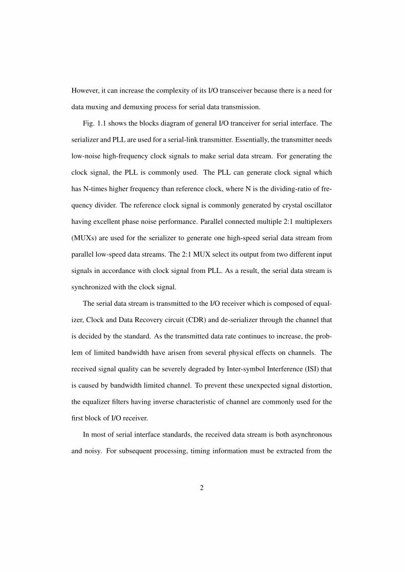
Fig. 1.1 shows the blocks diagram of general I/O tranceiver for serial interface. The
serializer and PLL are used for a serial-link transmitter. Essentially, the transmitter needs
low-noise high-frequency clock signals to make serial data stream. For generating the
clock signal, the PLL is commonly used. The PLL can generate clock signal which
has N-times higher frequency than reference clock, where N is the dividing-ratio of fre-
quency divider. The reference clock signal is commonly generated by crystal oscillator
having excellent phase noise performance. Parallel connected multiple 2:1 multiplexers
(MUXs) are used for the serializer to generate one high-speed serial data stream from
parallel low-speed data streams. The 2:1 MUX select its output from two different input
signals in accordance with clock signal from PLL. As a result, the serial data stream is
synchronized with the clock signal.
The serial data stream is transmitted to the I/O receiver which is composed of equal-
izer, Clock and Data Recovery circuit (CDR) and de-serializer through the channel that
is decided by the standard. As the transmitted data rate continues to increase, the prob-
lem of limited bandwidth have arisen from several physical effects on channels. The
received signal quality can be severely degraded by Inter-symbol Interference (ISI) that
is caused by bandwidth limited channel. To prevent these unexpected signal distortion,
the equalizer filters having inverse characteristic of channel are commonly used for the
first block of I/O receiver.
In most of serial interface standards, the received data stream is both asynchronous
and noisy. For subsequent processing, timing information must be extracted from the
2

2 X 2:1 Serializer
4 X
2:1
Se
rializ
er
8 X
2:1
Se
rializ
er
2:1
MU
X
Latch
Latch
D1
D0
OU
T
2:1 Serializer
2:1
MU
X
Latch
Latch
D1
D0
OU
T1
Output Driver
/2 /2 /2
16
-bit D
ata
@ 3
37
.5M
b/s
5GHz Clock
16
X 2
:1 S
eria
lize
r
PR
BS
Ge
ne
rato
r
/2 PLL
2 X
1:2
De
se
rializ
er
CD
R
4 X
1:2
De
se
rializ
er
/2/25GHz clock
8 X
1:2
De
se
rializ
er
/2/2
16
X 1
:2 D
es
eria
lize
r
BIS
T
Eq
ua
lize
r
Transmitter
Receiver
Figure 1.1: Block diagram of conventional I/O transceiver for serial interface
3
data so as to allow synchronous operations. Futhermore, the data must be retimed such
that the jitter accumulated during transmission is removed. The task of clock extration
and data retiming is called ”clock and data recovery”(CDR). Precise timing recovery is
one of the most critical components in serial communication because it is closely related
to the Bit Error Rate (BER) of the receiver. Thus, the CDR circuit is the most important
block of I/O receiver. A CDR circuit basically extract a clock signal which is aligned
to the data stream in frequency and phase by using feedback mechanism. The clock
signal is used to first re-time the data stream and then clock it into a high-speed digital
ASIC chip that performs desired processing operation. Also using the recovered clock
signal, parallelly connected multiple 1:2 de-multi-plexers (De-MUXs) generate parallel
low-speed data stream from the high-speed serial data stream. The 1:2 De-MUX split its
input in two output with the clock signal from CDR.
4
1.2 Overview of The Phase Detector for CDR Application
The goal of CDR circuit is generating synchronized clock signal from the received data
stream and re-sampling the received data with the recovered clock to filter out noises
in data. The block diagram of conventional CDR is shown in Fig. 1.2. Typically, a
CDR is formed by a phase detector (PD), a charge pump (CP), and loop filter (LF), and
a voltage controlled oscillator (VCO). The PD detects the phase difference between the
incoming data stream and the clock generated by the VCO, and produces a signal that
is used to dynamically adjust the frequency of the VCO so that in the end the phase
difference is kept constant and close to 0. In this feedback mechanism, the PD performs
very important function since it determines the direction of the feedback. In other words,
if the PD dose not produce precise phase difference information, the CDR may lose its
lock and can not generate clock signal synchronized with incoming data. Thus, the many
types of the PD have been researched for a long time.
Traditionally, two types of PDs have been widely used for CDR application. One is
analog PD called ’Hogge PD’, and the other is binary PD called ’Bang-Bang PD’. The
structure and characteristic of Hogge PD is shown in Fig. 1.3 (a). The Hogge PD has
two outputs X and Y. Since D-flip flop (DFF) produces a delayed replica of the input data
whose delay is determined by clock edges, X, one of Hogge PD’s output, contains pulses
whose width represents the phase difference between input data stream (Din) and VCO
clock (CK). The circuit produces a pulse for each data transitions, and the width of the
output pulses varies linearly with the input phase difference, suggesting that the circuit
can operate as a linear PD. However, if we use only ouptut X, two different phase errors
5

Φdata
Φclock
Phase Detector
Charge Pump
Loop
filter
Voltage Controlled
Oscillator
Clock Tree
Figure 1.2: Block diagram of typical CDR
6

D Q D QDin
CK
X
Y
D Q D QDin
CK
X
Y
D QD Q
Hogge PD structure
Bang-Bang PD structure
2π -2π ΔΦ
2π -2π ΔΦ
Hogge PD characteristic
Bang-Bang PD characteristic
Operating waveform
Din
CK
X
Y
Operating waveform
Din
CK
X
Y
(a)
(b)
Figure 1.3: PD comparison (a) Hogge PD (b) Bang-Bang PD
7

may result in the same dc output, leading to false lock. To avoid this, the proportional
pulses must be accompanied by reference pulses, which appear on data edges with a
constant width. To make this, the retimed data using first DFF is delayed by half a clock
cycle, TCK /2, and XORed with itself. Then pulses of width TCK /2 are produced for each
data transition. This can be used for reference pulse (Y), and under locked condition, X
and Y produce equal pulsewidths.
This topology achieves an infinite resolution phase error signal encoded in the width
of its ouptut error pulses, so that linear PD characteristic are obtained in a compact area
with minimal complexity and low power dissipation. Because it generates a vanishing
average as the phase difference approaches zero, a charge pump driven by a Hogge
PD experiences little activity when the CDR loop is locked. This behavior can reduce
VCO control voltage ripples resulting in reduction of jitters generated by CDR system.
Moreover, CDR system analysis and optimization can be easily achieved with linear
analysis. However, the need for a charge pump in linear CDR loops poses serious speed
limitaions. When the CDR loops is locked, the XOR output contains pulses only half
a bit periode wide, requiring a very broad bandwidth at these nodes to ensure complete
switching of the charge pump and hence avoid a dead zone.
CDR circuits incorporating Bang-Bang PD (BBPD) have found wide usage in high-
speed applications due to the speed limitation of Hogge PD. The structure and charac-
teristic of BBPD is shown in Fig. 1.3 (b). In the BBPD case, using three data samples
taken by three consecutive clock edges, the PD can determine whether a data transition
is present and whether the clock leads or lags the data. If the data edge leads the clock
edge, then BBPD output node X is high. Conversely, if the data edge lags the clock edge,
8
then BBPD output node Y is high. In the absence of data transitions, all three samples
are equal and no action is taken. The key point here is that the output of BBPD maintain
its level for one clock period. Thus, in principle, it can operate two times faster than
Hogge PD. In addition, BBPD has digital-friendly nature because the resulting phase er-
ror signals are three-level digital signals corresponding to whether a given data transition
is early, late, or absent relative to the clock phase within a given clock period.
Although BBPD implementation is very simple and digital, but, it has extremely
nonlinear characteristic. Because it can not detect the magnitude of phase difference
between clock and data, the output of BBPD in small phase difference case is just same
as large phase difference. It produces large ripples in VCO control voltages, resulting in
larger jitters generation. The most serious problem of BBPD’s nonlinear characteristic
is nonlinear dynamics for CDR system. Thus, A analysis and optimization of the BBPD
CDR is very difficult and its Process, Voltage, and Temperature (PVT) sensitivity is also
very high.
In summary, these two PDs have pros and cons. The Hogge PD can reduce the
jitters generated by CDR and it is suitable for optimizing CDR design due to its linear
characteristic. However, it suffers from speed limitation. On the other hands, the BBPD
can achieve a high-speed operation and a digital implementation, but the BBPD CDR
suffers from its high PVT sensitivity and low design reliability due to its non-linear
characteristic.
In order to take advantages of both PDs, the multi-level BBPD have recently re-
searched. [7] - [18] The multi-level BBPD can effectively linearize the BBPD response
by introducing more output levels in its phase error characteristic as shown in Fig. 1.4.
9
ΔΦ
Icp
(a)
BBPD BBPD BBPDD D D
Data
Clock
(b)
Delay Delay Delay
Icp1
Icp2
Icp3
Figure 1.4: (a) Characteristic of multi-level BBPD (b) Classical structure of multi-levelBBPD
10
Unlike linear PD whose phase error magnitude is represented by pulse width, the outputs
of multi-level BBPD have a 1-UI duration like conventional BBPD, and consequently,
it is still suitable for high-speed applications and digital implementations. In addition,
thanks to the PD gain linearization, we can apply the well-known linear, continuous time
analysis to CDR loop dynamics analysis, resulting in easy optimized CDR design. Also
the linearized PD gain can reduce the PVT sensitivity of CDR compared to CDR using
BBPD. Thus, it is called as ’improved BBPD’.
Usually, the multi-level BBPD uses simple buffers to create delayed versions of data
transmissions which are then compared to the VCO output clock phase using multiple
BBPDs as can be seen from fig. 1.4 (b) . It can be also implemented with phase inter-
polators or delay lines to create multi-phase of VCO output clock to detect magnitude
of phase errors. With this structure, the PD gain is determined by the output strength
of each BBPDs in multi-level BBPD which can be easily controlled by changing each
BBPD’s charge pump current. Unforunately, this approach carries the penalty of high
power consumption and high clock loading on the VCO output due to the large number
of BBPD elements running at high frequencies.
11

1.3 Outline of Dissertation
The main goal of this research is to investigate and develop a novel structure of multi-
level BBPD whose hardware cost is significantly reduced compared to the conventional
multi-level BBPD. For this, a 1.25Gb/s CDR with Time-Interleaving BBPD (TI-BBPD)
is proposed and its prototype is implemented in CMOS technology. The proposed multi-
level BBPD has effectively linear gain characteristics without much additional hardware
cost. In chapter 2, the basic concepts of CDR dynamics and comparison among the three
types of PDs will be reviewed. The operational principle and analysis of proposed BBPD
are introduced in chapter 3. In chapter 4, we will review the previous works for signal
monitoring circuit, and on-chip jitter monitoring using proposed multi-level BBPD are
introduced. In chapter 5, the detailed schematic-level circuits for the 1.25Gb/s CDR and
the simulation results are described. Finally, experimental results and conclusion are
given in chapter 6 and 7, respectively.
12
Chapter 2
Backgrounds and Motivations
2.1 Loop Dynamics and Noise Analysis of CDR
The performance of CDR, a key receiver timing circuit in clock-embedded serial link
systems, becomes critical to achieve optimal data sampling over various timing jitter
performance. Total jitter contains several components each with a different spectral
profile. To achieve the best timing margin over different jitter spectral profiles, it is
necessary to find the optimum loop dynamics of CDR.
2.1.1 Linear PD
The loop dynamics of CDR is determined by design parameters such as charge pump
current (Icp), VCO gain (Kvco), and PD gain (Kpd). Assuming that the PD has linear
characteristic, the CDR system can be represented with a small signal model as shown
in Fig. 2.1. In this approach, the PD can be expressed as a simple substracter with two
input are in the phase domain. Because s-domain analysis is continuous time analysis,
we assume that the charge pump flows continuous current over 2π period, and thus, the
13

Φdata
Φclock
Phase Detector
Icp
2π
sRC+1
sC
Charge pump Loop Filter
Kvco
s
VCO
Figure 2.1: Small signal model for CDR
gain of charge pump block has Icp/2π. The Loop filter transfer function can be easily
calculated because it is composed of passive elements only. Since the VCO block in this
approach has voltage input and phase output, the VCO can be represented as Kvco/s.
With this s-domain represented sub-blocks, we can calculate the transfer fucntion
between input data phase and output VCO clock phase in whole CDR system. It can be
depicted as
Hclosed(s) =2ζωn + ωn
2
s2 + 2ζωn + ωn2(2.1)
where ζ = R ·√Kpd · Icp · C ·Kvco, ωn =
√Kpd · Icp ·Kvco
C
As can be seen from eq. (2.1), the CDR system is 2-pole, 1-zero system and its
natural frequency ωn and damping ratio ζ are affected by design parameters. The transfer
function depicted in eq. (2.1) shows the relationship between the recovered clock phase
and the input data phase. Also, with this the linear, continuous time analysis of CDR, we
can obtain transfer functions for various input node. The transfer functions from various
input nodes shown in Fig. 2.2 can be derived as
14
Φdata
Φclock
Phase Detector
Icp
2π
sRC+1
sC
Charge pump Loop Filter
Kvco
s
VCO
Dinn
Icpn VLFn
ΦVCOn
Figure 2.2: Small signal model for CDR with various noise sources
Hin(s) =θoutDinn
=Hopen(s)
1 +Hopen(s)(2.2)
HCP (s) =θoutIcpn
=Hopen(s)/(Kpd · Icp)
1 +Hopen(s)(2.3)
HLF (s) =θoutVLFn
=Hopen(s)/(Kpd · Icp · ZLF )
1 +Hopen(s)(2.4)
HV CO(s) =θoutθV COn
=1
1 +Hopen(s)(2.5)
where, Hopen(s)= (Kpd Icp ZLF Kvco)/s and ZLF = (sRC+1)/sC. The transfer func-
tions are plotted in Fig. 2.3. For this simulation,Kpd = 1, Icp = 1mA,Kvco = 200MHz/V
are used for the design parameter. The transfer function between the input data phase
and the recovered clock phase has low pass filter characteristics as shown in fig. 2.3 (a),
it will filter out high frequency phase variation of input data. This characteristic is called
the ’jitter transfer’ of CDR. As can be seen in fig. 2.3 (b), the transfer function for the
charge pump current noise (Icpn) also has low-pass filter characteristice. This means that
we do not need to consider the fast changing Icp because this variation will be filtered out
by CDR feedback mechanism. On the other hand, the VCO noise is high-pass filtered
15

Figure 2.3: Noise analysis of linear-CDR (a) Input data vs. φout (b) Icpn vs. φout (c)Vcontn vs. φout (d) φV COn vs. φout
16

as can be seen in Fig. 2.3 (c). This indicate that slow jitter components generated by the
VCO are suppressed but fast jitter components are not. In the case of noises from loop
filter such as the thermal noise of resistor, it is band-pass filtered with peak frequency is
the CDR natural frequency ωn as can be seen from Fig. 2.3 (d).
To achieve optimum loop dynamics which makes CDR has largest timing margin,
firstly, we should carefully consider a noise contribution of each noise source. For ex-
ample, if the VCO phase noise is relatively larger than input data phase noise, wide ωn
is required for filtering the VCO phase noise as much as possible. On the other hand,
if the Icpn is serious, narrow ωn is required. ζ also can affect to the CDR performance
since too large or too small ζ makes jitter peaking at certain frequency.
As well as noise consideration, jitter generation and jitter tolerance of CDR should
be considered in order to achieve the optimum loop bandwidth. Jitter generation refers
to the jitter produced by a CDR circuit itself when the input random data contains no
jitter. The sources of jitter can be summarized as follows: (1) ripple on the VCO control
voltage, (2) coupling of data transitions to the VCO through the PD, (3) supply and
substrate noise. Jitter tolerance specifies how much input jitter a CDR loop tolerates
without increasing the BER. Thus, we can assume that a CDR with high jitter tolerance
has a large timing margin. Unfortunately, there is a trade-off between jitter tolerance
and jitter generation. Typically, the CDR having wide ωn is desired to achieve high jitter
tolerance, but wide ωn can increase jitter generation of CDR because of its small loop
filter capacitor and large resistor, resulting in jitter tolerance degradation. Therefore,
designer should carefully determine the loop dynamics with considering the trade-off.
Fig. 2.4 shows the timing margin variation of CDR under various loop dynamcis
17

Figure 2.4: Recovered clock rms jitter vs. loop dyanmics setting
18

condition. The result comes from behaviral simulation. Each CDR blocks such as PD,
CP, VCO are coded using Verilog-A language, and the timing margin is measured by
phase difference between the input data and the recovered clock by using an ideal phase
difference calculator also coded using Verilog-A. For this simulation, the Icp = 1mA,
Kvco = 100MHz/V and the VCO has a random jitter noise source and input data do
not have. As for the ωn, too large ωn makes large jitter generation, resulting in timing
margin degradation. Too small ωn also degrade CDR performance because VCO noise
in not sufficiently filtered out. In terms of ζ, too large ζ makes large jitter generation
and too small ζ makes large jitter peaking, and consequently, there is optimum value of
ζ and ωn to achieve largest timing margin.
2.1.2 BBPD
Since changing the value of ωn and ζ has serious effects on the CDR performance, de-
signer should carefully determine the loop filter characteristic considering each design
parameters such as Kpd, Kvco, and Icp. In linear PD-CDR case, if the noise character-
isitc of each blocks in CDR is well-modeled, it is relatively easy to determine design
parameters and loop filter value because the well-known linear analysis can apply to the
linear-PD CDR. However, the presence of the BBPD introduces a hard non-linearity in
the loop, the ωn, ζ cannot be defined in a strict sense. Because the frequency domain
approach can not be used for BBPD CDR, the analysis completely in time domain is
recently researched. [1] - [3]
The time domain analysis introduce the concept of orbit in an appropriate phase
plane. With this, it intends a trajectory on the phase plane which repeats itself. This
19

research has been found that the second-order BBPD CDR can show three different
behaviors: unstable, stable with unbounded orbits, stable with bounded orbits. These
three different behaviors are determined by the ’loop delay’ which means the number of
reference clock appearance during the 1-cycle of CDR feedback operation.
Although these time domain analysis for BBPD CDR have been recognized, this
research does not provide sufficient insight for designing BBPD CDR. Designers still
want to have ways to explain them in linear control term, such as bandwidth for fre-
quency response and damping factor for stability. A way of describing BBPD CDR in
the context of linear control theory by using effective linearized gain concept for BBPD
is also presented in [4], [5].
The linear region of BBPD is generated by two phenomena as explained in [4]. First,
when the zero-crossing points of the recovered clock fall in the vicinity of data transi-
tions, the flip flops comprising the PD may experience metastability, thereby generating
an output lower than the full level for some time. In other words, the average output
generated by the BBPD remains below the saturated level for a small phase difference
between input data and recovered clock.
Fig. 2.5 illustrates three distinct cases that determine certain points on the BBPD
characteristic. If the phase difference between clock and input data, ∆T , is large enough,
the latch output reaches the saturated level, VF , in the sampling mode as shown in fig. 2.5
(a). By contrast, if ∆T is small, the regeneration in half a clock period does not amplifiy
latch output to VF because of metastability of practical latch circuits. The smaller ∆T is
the lower the latch output in regerenation mode is as can be seen in fig. 2.5 (b), (c). Since
the current delivered to the loop filter is proportional to the area under difference between
20

ΔT
Latch
output
CK
Sense Hold
VF
(a)
ΔT
Latch
output
CK
Sense Hold
VF
(b)
ΔT
Latch
output
CK
Sense Hold
VF
(c)
ΔT
VPD
ΔTLIN ΔTSAT
VF
(d)
Figure 2.5: (a) BBPD output for a completely differential pair switching (b) BBPD out-put for partial differential pair switching (c) BBPD output for incomplete regeneration(d) Typical BBPD characteristic.
21

two latch outputs (if the latch is fully differenctial), the average output is indeed linearly
proportional to ∆T . Fig. 2.5 (d) summarizes these concepts. ∆TLIN and ∆TSAT can
be depicted as
∆TLIN =VF
2 · k ·Apre · exp(Tb/2τreg)(2.6)
∆TSAT =VF
2 · k ·Apre(2.7)
where, 2kApre is the slew rate of latch circuit, τreg is regeneration time constant, and Tb
is one bit period.
The binary PD characteristic is also smoothed out by the jitter inherent in the input
data and the VCO output. Even with abrupt data and clock transitions, the random phase
difference resulting from jitter leads to an average output lower than the saturated levels.
As illustrated in Fig. 2.6 (a), for a phase difference of ∆T , it is possible that the tail of
the jitter distribution shifts the clock edge to the left by more than ∆T , forcing the PD to
sample a level of -V0 rather than +V0. To obtain the average output under this condition,
we sum the positive and negative samples with a weighting given by the probability of
their occurrences:
VPD(∆T ) = −V0
∫ −∆T
−∞p(x)dx+ V0
∫ ∞−∆T
p(x)dx (2.8)
where p(x) denotes the probability density function (PDF) of jitter. As a result, the
BBPD characteristic exhibits a relatively linear range as shown in fig. 2.6 (b).
Fortunately, the BBPD CDR operates within the linear range of BBPD under the
22

Probability of
sampling -V0
Din
CK
(a)
ΔT
VPD VF
(b)
-ΔT
-V0
+V0
Figure 2.6: Smoothing of PD characteristic due to jitter
23

lock condition, this concept allows for linear analysis of non-linear bang-bang control
loop in a statistical sense.
2.1.3 Multi-Level BBPD
Although the effectively linearized BBPD gain analysis gives insight for designing BBPD
CDR, the BBPD CDR still exhibits highly non-linear behavior especially in large ωn and
ζ case since the phase difference between input data and VCO clock (phase error) in this
case can be larger than effective linear region of BBPD. Also, the BBPD CDR experi-
ences relatively large jitter generation compared to linear PD-CDR and the statistically
calculated effective PD gain is very sensitive to environmental factors such as PVT and
jitter distribution of input data and VCO. Thus, BBPD CDR loop dynamics is still unpre-
dictable and sensitive to environment. The ultimate cause of all these is that the BBPD
cannot detect the magnitude of phase error. Since it does not know how much timing is
off by, the updated VCO phase amount could be too large for small phase error, or too
small for large phase error.
The multi-level BBPD can be a solution for this problem. Since the multi-level
BBPD can detect both direction and magnitude of the phase error as shown in fig. 1.4,
the Multi-level BBPD CDR can be analyzed using well-known linear analysis same
as linear PD-CDR. This is prime benefit of the multi-level BBPD. Thanks to its linear
characteristic, it has high design reliability as explained in previous chapter.
24

2.2 Performance Comparison Among Three Types of PDs
2.2.1 Environmental Sensitivity
The CDR loop dynamics has a great influence on the CDR performance. Fig. 2.7
shows the CDR performance variation comparison among three types of PD (Linear PD,
BBPD, Multi-level BBPD) under various loop filter condition. This simulation result
comes from behavioral models of three PDs, CP, and VCO coded using Verilog-A. For
this simulation, 3 different CDRs have same CP, VCO and Icp=1mA, Kvco=100MHz/V.
The multi-level BBPD has 8-level outputs. For easy timing margin measurement, the
input data do not have noise source in this simulation. With this simulation setting, we
can assume that the large recovered clock jitter means the small timing margin of CDR.
In this simulation, the loop filter changes only its resistor value. The resistor value
changes from 250 Ω to 500 Ω. The recovered clock jitter of BBPD CDR is changed from
26.6ps to 37.08ps, while other PDs whose recovered clock jitter is nearly constant. This
high loop filter sensitivity is due to BBPD’s extremely high Kpd.
The high loop filter sensitivity of CDR can be a serious problem since the loop filter
is usually designed by on-chip resistor and capacitor whose PVT sensitivity is very high,
especially an on-chip resistor. The designer should determine the loop filter value to
achieve best performance of CDR, but in BBPD CDR case, the designer can not have a
enough margin for the loop filter value range.
Fig. 2.8 shows the loop dynamics variation of each CDRs under PVT variation.
We assume that the loop filter resistor experiences ±5% variation and the capacitor
experiences ±2.5%. To calculate loop dynamics by using ideal spice model, the de-
25

sign parameters of each behavioral blocks such as Icp, Kpd, Kvco is extracted from the
transistor-level simulation. A sampler used in each PDs is designed as sense-amplifier
based D-flipflop. We simulate 3 case of PVT variation: (1) Case-I: SS corner, 1.7V
supply, 40C (2) Case-II: TT corner, 1.8V supply, 20C (3) Case-III: FF corner, 1.9V
supply, 0C
As can be seen in the figure, the loop dynamics of linear PD-CDR and multi-level
BBPD CDR does not change significantly. The bandwidth of linear PD-CDR is changed
from about 28.2MHz to 30.2MHz, and that of multi-level BBPD CDR is changed from
about 27.5MHz to 31MHz. On the contrary, the BBPD CDR experiences relatively large
loop dynamics variation. The bandwidth of BBPD CDR is changed from about 25MHz
to 32MHz. The PVT sensitivity of BBPD CDR loop dynamics is about 2 times larger
than other CDRs. The dominant factor of BBPD CDR’s high PVT sensitivity is Kpd
variation. The Kpd of BBPD is affected by metastability of D-flipflop which is very
sensitive to PVT variation. In multi-level BBPD case, theKpd is dominantly determined
by the output strength of each BBPDs in multi-level BBPD, not a metastbility of D-
flipflop.
The jitter magnitude of input data and VCO also has a great influence on the loop
dynamics of BBPD CDR. In the linear PD-CDR, the Kpd remains constant in a noisy
environment, i.e., independent of jitter pdf. However, in BBPD CDR, the effective Kpd
changes with the input jitter pdf, which affects loop dynamics. The jitter transfer charac-
terisitcs of each CDRs are shown in fig. 2.9. For this simulation, the design parameters
under TT corner, 1.8V supply, 20C condition is used for each CDRs. The magnitude
of VCO random jitter is changed by 3-cases, and the resulting Kpd of each PDs are
26

recorded. We calculate the loop dynamics by matlab according to the Kpd variation.
As can be seen in the figure, the loop dynmics of linear PD-CDR dosen’t changed
because the linear-PD is not affected by the jitter magnitude as mentioned above. The
multi-level BBPD CDR experience a little loop dynamics variation since the its multiple
BBPDs experience a little Kpd variation by the jitter variation. But, the multiple BBPDs
can diffuse the effect of jitter. The variation in loop dynamics can be reduced by in-
creasing the output levels of multi-level BBPD as explained in [5]. On the other hand,
the magnitude of VCO jitter seriously affect the loop dynamics of BBPD CDR as can
be seen in fig. 2.9 (b) since the jitter distribution can change the Kpd of BBPD severely.
While the bandwidth of multi-level BBPD CDR changes from 29.5MHz to 21.4MHz,
that of BBPD CDR is varied from 29.5MHz to 12.6MHz.
In conclusion, due to the sensitive Kpd, the loop dynamics of BBPD CDR is varied
strongly with the environment factors such as PVT variation and jitter distribution com-
pared to Linear-PD CDR and Multi-level BBPD CDR. Since we can not predict the PVT
variation and jitter distribution, the uncertainties in the effective Kpd make it diffcult to
choose other design parameters to achieve the optimum loop dynamics.
27

Figure 2.7: Recovered clock rms jitter of 3 types of CDR under various loop filter resis-tance
28

Figure 2.8: Loop dynamics variation under PVT variation (a) Linear-PD CDR (b) BBPDCDR (c) Multi-level BBPD CDR
29

Figure 2.9: Loop dynamics variation under various jitter distribution (a) Linear-PD CDR(b) BBPD CDR (c) Multi-level BBPD CDR
30

2.2.2 Maximum Operating Speed and Power Consumption of CDRs
As mentioned previously, the linear PD-CDR has a serious speed limitation since the
XOR outputs contain pulses only half a bit period wide under locked condition. The
narrow pulse of linear PD output can not sufficiently open the switch in CP. On the other
hands, BBPD CDR and multi-level BBPD CDR can have a relatively high operating
speed since their PDs generate 1-UI duration XOR output under locked condition.
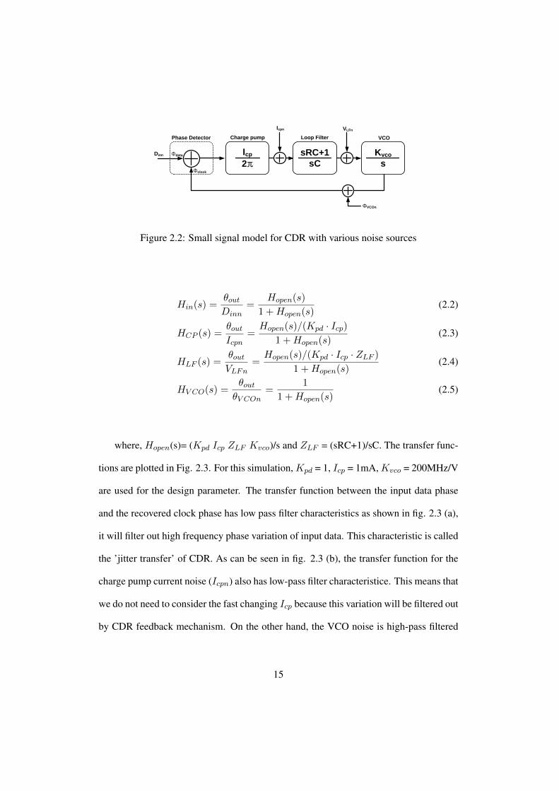
Fig. 2.10 (a) shows the maximum operating speed of 3-types of full-rate CDRs. For
this simulation, the each PDs and CP are designed with 0.18µm CMOS technology. To
reduce the simulation time, we used verilog-A coded VCO and 27-1 PRBS data as a
input. As expected, the BBPD CDR can operate at the highest input data rate. The max-
imum operating speed of BBPD CDR is about 3.2Gb/s. That of multi-level BBPD CDR
is 2.9Gb/s which is a little less than BBPD CDR. The reason for this speed degradation is
a large interconnection capacitance due to its complex structure. On the other hand, the
Linear-PD CDR cannot operate at even 1.5Gb/s which is a half of maximum operating
speed of BBPD CDR. Its maximum operating speed is observed at 1.3Gb/s.
To avoid CP dead zone which makes the loop gain drops to zero, the PD output
should have a certain level of pulse width. As data rate becomes higher, the pulse width
of linear PD output reaches the minimum level of pulse width much faster than in the
case of BBPD or multi-level BBPD due to the pulse width margin difference. For exam-
ple, if the required minimum pulse width of the CP is 0.2UI, the pulse width margin of
BBPD and multi-level BBPD is 0.8UI, while that of linear PD is only 0.3UI.
The power consumption of each PD-CDRs at the maximum operate speed is shown
31

in fig. 2.10 (b). For this simulation, the power consumption of the BBPD and linear PD
is designed as same as possible. The simulation result shows that the BBPD consumes
4.32mW and the Linear PD consumes 3.92mW. Contrastively, the multi-level BBPD
which has 8 output levels consumes 30.7mW since it is composed of 7-BBPD, 7-CP,
7-delay lines. With this result, we can calculate the power efficiency that represents the
ratio of maximum operating speed and power consumption. As can be seen from the
fig. 2.10 (c), the power efficiency of linear PD, BBPD, and multi-level BBPD are cal-
culated as 0.7Gbps/mW, 0.3316Gbps/mW, and 0.09Gbps/mW, respectively. The power
efficiency of multi-level BBPD CDR is seriously degraded in comparison with BBPD
due to its large hardware cost. Table 2.1 shows the performance summary of these 3-
PDs.
32
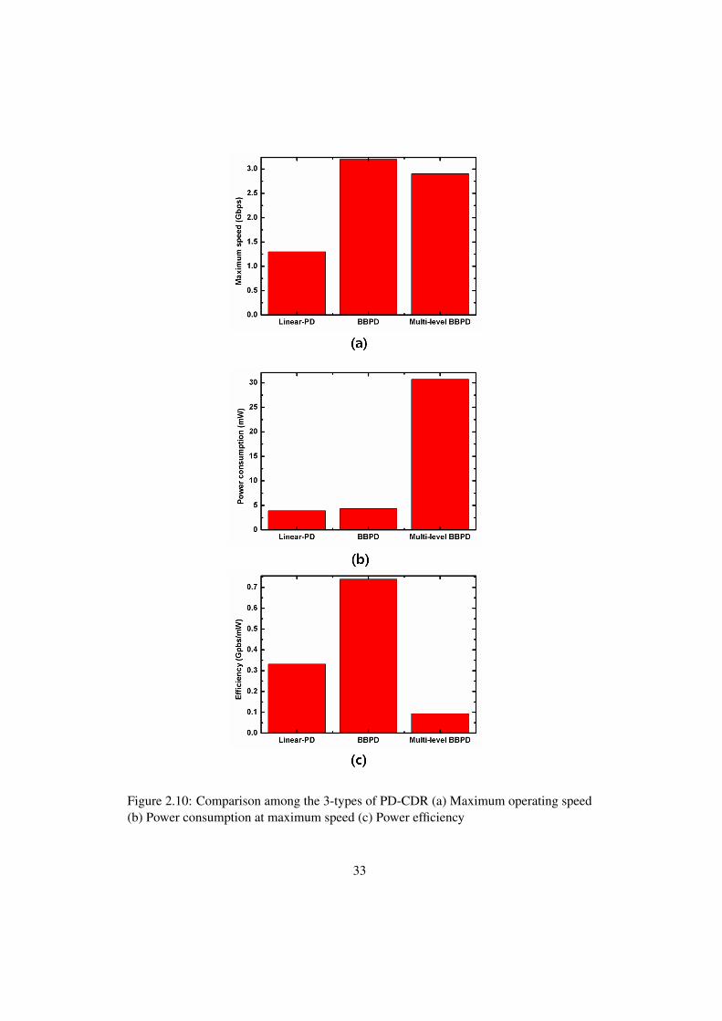
Figure 2.10: Comparison among the 3-types of PD-CDR (a) Maximum operating speed(b) Power consumption at maximum speed (c) Power efficiency
33

Linear PD BBPD ML-BBPD
PD characteristic Linear Non-linear Linear
Loop filter sensitivity
(Variation rate (%)) 6% 40% 2%
PVT sensitivity
(ωn Variation (MHz)) 2 MHz 7 MHz 3.5 MHz
Jitter sensitivity
(ωn Variation (MHz)) 0.7 MHz 16.9 MHz 8.1 MHz
Maximum speed (Gbps) 1.3 3.2 2.9
Power consumption (mW) 3.92 4.32 30.7
Power efficiency (Gbps/mW) 0.3316 0.74 0.094
Table 2.1: Performance comparison among three-types of PD-CDR
34

Chapter 3
CDR with a New Multi-Level BBPD
3.1 Time-Interleaved Multi-Level BBPD
3.1.1 Operational Principle
Conventionally, multi-level BBPD is composed of multple BBPDs, CPs, and delay lines
as shown in fig. 3.1 (a). As mentioned previously, this structure consumes large power
and ocuppies large chip area. A more serious problem of this structure is that the hard-
ware requirement is directly proportional to the number of BBPD output levels. If we
want to generate one more output level, one BBPD, one CP, one delay line are addition-
ally required. For achieving robust and reliable design of CDR, a large number of output
levels is clearly desired since we can obtain more linearized characteristics of PD, but it
increases power consumption seriously. Furthermore, it causes operating speed degra-
dation due to the a large load capacitor for input data. Thus, there are large trade-off
between power consumption and CDR performance in this structure. Most of previously
reported multi-level BBPD [9] - [17] didn’t overcome this trade-off, and consequently,
most of them reported the multi-level BBPD having only 5 or 6 levels.
To overcome the trade-off, we develop the multi-level BBPD whose multiple output
35

Integration
CP
CP
CP
CP
CP
CP
Delay
BBPD
BBPD
BBPD
BBPD
BBPD
BBPD
BBPD+CP
VCO
Received
data
(a)Integration
CP
CP
CP
CP
CP
CP
Delay
BBPD+CP
VCO
Received
data
(b)
Figure 3.1: Conceptual illustration for generating multi-level PD output (a) Conventionalmethod (b) Proposed method
36

levels is generated by the time-interleaving method. The conceptual block diagram of
proposed BBPD is shown in fig. 3.1 (b). The whole structure is identical to the con-
ventional BBPD structure composed of one BBPD, one CP, and one delay line which
delay can be digitally controlled. To make multiple output levels, the delay of delay line
is continuously varied in this structure. In other words, the clock phase applied to the
BBPD is continuously changed, and consequently, the Icp is also dynamically changed.
Fig. 3.2 shows the Icp waveforms of conventional structure and proposed structure.
The conventional structure generates constant Icp. If the phase error is increased, the
constant output Icp is also increased with certain current step. On the contrary, the
proposed structure generates dynamically changed Icp as shown in fig. 3.2 (b). In this
case, if the frequency of moving Icp is sufficiently lower than ωn of CDR, the moving
Icp can be treated as constant Icp,avg which is average value of moving Icp. The Icp,avg
can represent the magnitude of phase error same as Icp of conventional structure. As can
be seen in the figure, if the phase error is increased, Icp,avg is also increased since the
high Icp appears more frequently than low Icp.
With this structure, we can significantly reduce the hardware cost of multi-level
BBPD especially in a large number of output levels case. The number of proposed
BBPD’s output levels can be expressed as
Nlevel = 2 + 2NBG (3.1)
where Nlevel is the number of output levels, and NBG is the number of control bit for
digitally controlled delay line. The designed BBPD basically has 2-levels due to BBPD,
and theNlevel can be exponentially increased forNBG. Because we simply design a little
37

Total Icp
Time
Total Icp
Time
Total Icp
Time
Ph
as
e e
rro
r is
larg
er
Total Icp
Time
Total Icp
Total Icp
Time
Time
Ph
as
e e
rro
r is
larg
er
(a)
(b)
Icp,avg
Icp,avg
Icp,avg
Figure 3.2: Waveform of Icp (a) Conventional method (b) Proposed method
38

more complex control signal generator for increasing NBG, it dose not require much
hardware cost. Thus, we can design the multi-level BBPD having a large number of
output levels without much hardware cost by using proposed time-interleaving method.
39

3.1.2 Implementation of Time-Interleaved BBPD
For implementation, we proposed a Time-Interleaved BBPD (TI-BBPD) which can make
a large number of output levels with one BBPD, one Dead-Zone PD [26]-[28] (DZPD),
and dead-zone width controller. The overall structure of the proposed PD is showin in
fig. 3.3 (a).
The dead-zone PD, which is known as a 3-over sampling PD, produces Icp only when
the data transition is out of its dead-zone. To do that, it needs two sampling clocks which
are placed around data edge to make right and left dead-zone width. Conventionally, it
need one more sampling clock (this is the reason it is called 3-over sampling PD) to
retime the input data, but our structure doesn’t need this clock because BBPD performs
the data retiming.
The dead-zone width controller is composed of a variable dead-zone generator and
a bit generator. Because the dead-zone width is determined by the phase difference
between left side clock (Lclk) and right side clock (Rclk), which are applied to DZPD,
variable dead-zone width can be easily controlled by moving the phase of each clock.
The variable clock phase generator can be implemented with a digitally controlled phase
interpolator or digitally controlled delay line. The bit generator generates N-signals
to control the phase of Rclk and Lclk. Unlike the classical multi-level BBPD whose
parallel control bits maintain constant values, the proposed multi-level BBPD has its
serial control bit changing synchronized with the M-divided recovered clock. With these
two blocks, the dead-zone width controller produces two sampling clocks which keep
changing its phase to generate variable dead-zone of the DZPD as shown in fig. 3.3 (b).
40

Variable
dead-zone
generator
Bit generator
BBPD DZPDD D
%M
ΦN
ΦN
Φ1Φ1
fdata
fclock
N signals
Dead-zone
width
controller
BBPD clock
Integration
Icp2
Icp2
Icp1
Icp1
M cycles
2Φ1
2Φ2
2ΦN
fclock
fclock/M
Dead-zone
width
-45° 45° 0°
1 2 N 1 2
(a)
(b)
Figure 3.3: (a) A architecture of Time-Interleaved BBPD (TI-BBPD) (b) Operation ofdead-zone width controller
41
Each PD’s output is connected to two different CPs. The BBPD’s output is con-
nected to CP whose current (Icp1) is relatively small and the DZPD’s output generates a
relatively large current (Icp2). With this structure, we can effectively make many levels
of BBPD output in statistical manner without much hardware cost.
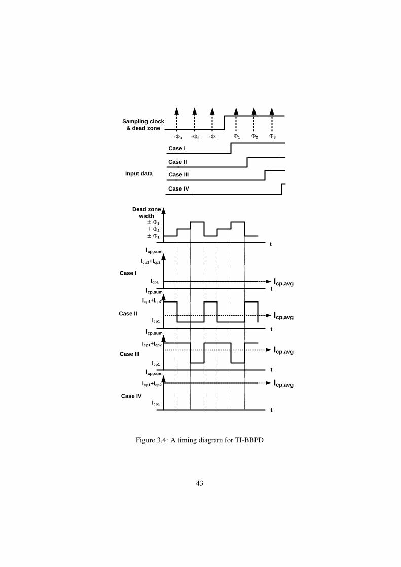
Fig. 3.4 shows the timing diagram of TI-BBPD. This figure shows the case of 8-
level BBPD as an example. In this case, the dead-zone width changes from 2φ1 to 2φ3
repeatedly. If the phase error is very small, than the data edge does not exist out of
any dead-zone width, and consequently, the DZPD output doesn’t appear. In this case,
the total charge pump current (Icp,sum) maintain its value as Icp1. In case-II, the phase
error is a little larger than case-I. Because the phase error is larger than φ1, the DZPD
generates its output when its dead-zone is 2φ1. As a result, Icp,sum maintains its output
as Icp1+Icp2 during M-cycles of recovered clock, and as Icp1 during 2M-cycles as shown
in fig. 3.4. Thus, the average charge pump current (Icp,avg) becomes larger compared
to Icp,avg in case-I. If the phase error is within φ2 and φ3, DZPD generates Icp2 when
its dead-zone width is 2φ1 and 2φ2. In this case, the duration of Icp1+Icp2 is two times
longer than that of case-II, resulting in large Icp,avg compared to case-II. Lastly, if the
phase error is larger than φ3, DZPD always generates its output and Icp,avg becomes
Icp1+Icp2. In summary, Icp,avg changes according to the magnitude of phase error with
this structure.
Fig. 3.5 show the PD characteristic of TI-BBPD in general case. The dead-zone
width changes from 2φ1 to 2φ2, 2φ3, ..., 2φN . The whole operation repeats itself every
M × N recovered clock cycle. Since DZPD produces charge pump currents when the
data transition is out of its dead-zone, its charge pump current when averaged over M ×
42
Dead zone
width
± Φ1
± Φ2
± Φ3
t
Icp,sum
t
t
Icp,sum
Icp,avg
Icp,avg
Sampling clock
& dead zone
Input data
Φ1 Φ2 Φ3-Φ1-Φ3 -Φ2
Case II
Case I
Case IV
Case III
Icp,sum
t
Icp1+Icp2
Icp,avg
t
Icp,sum
Icp,avg
Case II
Case I
Case III
Case IV
Icp1
Icp1+Icp2
Icp1
Icp1+Icp2
Icp1
Icp1+Icp2
Icp1
Figure 3.4: A timing diagram for TI-BBPD
43

Φ1 Φ2Δ Φ
-Φ1
Icp1
-Φ2
Δ Φ
Δ Φ
VDML-BBPD
Icp1
-Icp1
ΦN
-ΦN
ΦN-1 ΦN
Icp1+Icp2
BBPD
DZPD
Icp2/N
-Icp2/N
-ΦN-1-ΦN
-Φ1
Φ1
2Φ1
2ΦN
SUM
-Icp1
-(Icp1+Icp2)
Figure 3.5: PD gain characteristic of TI-BBPD
44

N unit intervals becomes Icp2/N. When these charge pump currents are added with Icp1,
the total PD characteristic have multi levels as shown in the figure. With this method, we
can simply obtain many levels of BBPD output by increasing the number of dead-zone.
45

3.1.3 The Gain of TI-BBPD
The Kpd of TI-BBPD can be calculated as the previously reported BBPD. In 8-level
TI-BBPD, Icp,avg of each level can be expressed as,
Icp,L1 = Icp1 + 0 · Icp2, (3.2)
Icp,L2 = Icp1 + PDZ1 · Icp2,
Icp,L3 = Icp1 + PDZ1 · PDZ2 · Icp2,
Icp,L4 = Icp1 + PDZ1 · PDZ2 · PDZ3 · Icp2,
where Icp,Ln is the n-th level average Icp and PDZn is the appearance probability of
n-th dead-zone width during M × N recovered clock cycles. In an additional explanation
for PDZn, if the dead-zone width is changed to next dead-zone width every M cycles
of recovered clock like a example of previous chapter, PDZn has the same apperance
probability of 1/N. In contrast, if 2nd dead-zone width maintains its value during more
than M cycles of recovered clock, PDZ2 is larger than other PDZn’s. With the equations
in eq. (3.2), we can derive the general equation of Icp,Ln as
Icp,Ln = Icp1 +n−1∑n=0
PDZn · Icp2 (3.3)
As can be seen from eq. (3.3), Icp,Ln is determined by the Icp of each PDs and
the apperance probability of each dead-zones. With this equation, we can calculate the
current difference between two adjacent levels,
46

Icp,L(n+1) − Icp,Ln = Icp1 +n∑n=0
PDZn · Icp2 − (Icp1 +n−1∑n=0
PDZn · Icp2) (3.4)
= PDZn · Icp2
If we assume that the each level of TI-BBPD is smoothed due to metastability and
jitter distribution as can be seen in fig. 3.6 (a), the Kpd of TI-BBPD between φn to φn+1
can be derived as
Kpd =PDZn · Icp2φn+1 − φn
(3.5)
The Kpd is determined by PDZn, Icp2, and phase step of the n-th level. To simplify
the gain analysis, we assume that the phase step of each levels are same and independent
of PDZn. For this, all PDZn of each dead-zone should have the same value 1/N. For
example, in 12-level case, PDZ1=PDZ2=PDZ3=PDZ4=PDZ5=0.2. And if we want to
have the same current difference of each level from first level to last level with all same
PDZn, Icp2 should be determined as eq. (3.6).
PDZn · Icp2 = 2 · Icp1 (3.6)
Icp2 =2
PDZn· Icp1
Since the Kpd is affected by PDZn, it can be easily controlled. For example, in 12-
level case, if we set the probability as PDZ1=PDZ2=PDZ3=PDZ4=0.1, and PDZ5=0.6,
the PD gain from φ0 to φ4 will be decreased, and the PD gain from φ4 to φ5 will be
47

(a)
Δ ΦΦN-1 ΦN ΦN+1
PD
gain
Φ1 Φ2Δ Φ
-Φ1-Φ2
ΦN-1 ΦN
-ΦN-1-ΦN
(b)
All PDZn=1/N
Figure 3.6: Kpd estimation
48

increased. Although, this makes some non-linearity at the end of linear region, the phase
error rarely goes into this range under CDR locked condition.
The simulation results with ideal CDR blocks are shown in fig. 3.7. In this simula-
tion, the 12-level TI-BBPD is designed with Icp1=30µA, Icp2=240µA and all PDZn=0.2
for fig. 3.7 (a) and PDZ1=PDZ2=PDZ3=PDZ4=0.1, PDZ5=0.6 for fig. 3.7 (b). The sim-
ulated PD characteristic has a stair shape because there are no metastability of D-filpflop
and jitter. Icp,Ln of each levels are well matched with eq. (3.3) in both (a) and (b) case.
The maximum current is (240+30)/2 µA because the data transition density is 0.5. These
results imply that the Kpd can be easily predicted and also it can be easily controlled by
changing generated bit squence of bit generator in dead-zone width controller. In ad-
dtion, the PVT sensitivity will be reduced by using our TI-BBPD. Because the Kpd is
determined by the completely digital controlled PDZn, the Kpd also has high PVT im-
munity compared to classical multi-level BBPD whose Kpd is determined by difference
between two adjacent charge pump current.
49

Figure 3.7: Simulation results of TI-BBPD characteristic (a) When all PDZn is same (b)When PDZ5 has larger probability
50

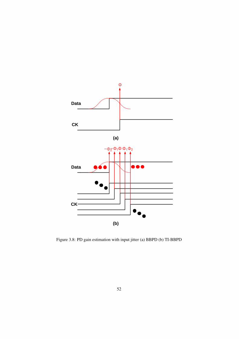
3.1.4 Input Jitter Sensitivity of TI-BBPD
The jitter distribution of input data and VCO has serious effects on Kpd changing in
BBPD case. The expected charge pump current at the phase Φ (Icp(Φ)) in fig. 3.8 can
be calculated as
Icp(Φ) = Icp
∫ Φ
−∞p(x)dx− Icp
∫ ∞Φ
p(x)dx (3.7)
where the p(x) is pdf of jitter distribution. With this equation, we can derive the PD gain
of BBPD (KBBPD) as
KBBPD =Icp(Φ + ∆Φ) − Icp(Φ)
∆Φ(3.8)
=2 · Icp
∫ Φ+∆ΦΦ p(x)dx
∆Φ
According to eq. (3.8), we can find that the jitter distribution sensitivity of KBBPD is
proportional to Icp. Thus, to reduce that, we should reduce the Icp. But reducing Icp can
increase the in-band noise sensitivity of CDR system.
The TI-BBPD has a different characteristic. Fig. 3.8 (b) shows the timing diagram
of TI-BBPD. In the same situation, the expected charge pump current at the phase Φ
(Icp(Φ)) can be calculated as
Icp(Φ) = Icp,L1
∫ Φ
Φ−Φ−1
p(x)dx+ Icp,L2
∫ Φ−Φ−1
Φ−Φ−2
p(x)dx+ ... (3.9)
+ Icp,L1
∫ Φ+Φ1
Φp(x)dx+ Icp,L2
∫ Φ+Φ2
Φ+Φ1
p(x)dx+ ...
51
Φ
Data
CK
(a)
Φ
Data
CK
(b)
-Φ1 -Φ2 Φ1 Φ2
Figure 3.8: PD gain estimation with input jitter (a) BBPD (b) TI-BBPD
52

Because the jitter effect onKpd is analyzed with statistical manner, Icp of each levels
can be treated as a constant value which can be calculated by using eq. (3.3). With this,
we can derive the PD gain of TI-BBPD (KTI ) with the assumption that the phase step
of multi-level BBPD is much larger than ∆Φ:
KTI =Icp(Φ + ∆Φ) − Icp(Φ)
∆Φ(3.10)
= (Icp,L1(P (Φ + ∆Φ) − P (Φ + ∆Φ − Φ1) − P (Φ) + P (Φ − Φ1))+
Icp,L2(P (Φ + ∆Φ − Φ1) − P (Φ + ∆Φ − Φ2) − P (Φ − Φ1) + P (Φ − Φ2))...)/∆Φ
=2 · Icp,L1
∫ Φ+∆ΦΦ p(x)dx
∆Φ
According to eq. (3.10), the jitter sensitivity of KTI is proportional to Icp,L1. Be-
cause the first level current of TI-BBPD is very small compared to Icp of classical BBPD,
the sensitivity will be significantly alleviated.
Fig. 3.9 shows the simulation results of jitter sensitivity comparison between the
BBPD and TI-BBPD. In this simulation, Icp of BBPD is 240 µA, Icp1 and Icp2 of TI-
BBPD is 30 µA, 240 µA, respectively. As can be seen from the figure, the KBBPD
changes rapidly with jitter magnitude. By contrast, KTI is almost constant. KBBPD in
normal jitter case is 17.845 µA/UI and 8.0192 µA/UI in worst jitter case. The variation
rate of KBBPD is 1.96515. On the other hand, The KTI is changed from 4.8 µA/UI
to 3.8 µA/UI in same jitter magnitude variation. The gain variation rate is 0.21. As
expected, the jitter sensitivity ofKBBPD is about 8 times larger than that ofKTI because
the Icp is 8 times larger than Icp,L1.
If the jitter is very large, the PD gain linearization by the jitter can become similar
53

Figure 3.9: Simulation results for PD gain with jitter (a) BBPD (b) TI-BBPD
54

Figure 3.10: Kpd simulation with various input data rate (a) 1-Gbps data rate (b) 4-Gbpsdata rate (c) 7-Gbps data rate (d) 10-Gbps data rate
55

to that by using the TI-BBPD. Fig. 3.10 shows the simulation results of comparison
between the characteristic of BBPD and TI-BBPD under various input data rate. In this
simulation, we set that the absolute magnitude of VCO rms jitter is fixed to 20ps which
is 0.02UI for 1Gbps data rate, and 0.2UI for 10Gbps. As the data rate is increased, the
characteristic of BBPD and TI-BBPD becomes similar as shown in the figure. Although
these results can be accepted that the TI-BBPD is not necessary in noisy environment
conditon, but, the important thing is that we can not predict the jitter magnitude gener-
ally. Because the Kpd of TI-BBPD has much higher immunity for the jitter magnitude
as compared with that of BBPD, the design reliability of TI-BBPD is much higher. In
other words, the Kpd of TI-BBPD can be treated as a design parameter, while that of
BBPD is not.
56

3.2 CDR with TI-BBPD
3.2.1 Performance Simulation of TI-BBPD CDR
To verify the effect of TI-BBPD on a CDR, same simulations in chapter 2.2 are per-
formed. Fig. 3.11 shows the loop filter setting sensitivity of TI-BBPD CDR. In this
simulation, Icp1 and Icp2 of TI-BBPD is 30 µA, 240 µA, respectively. The bit genera-
tor generate 3-bit PI control signal so that the TI-BBPD have effectly 18 output levels.
This simulation is performed with behavioral models using Verilog-A. For easy mear-
surement, we used the behaviroal model of VCO has random jitter noise source, and
the ideal 1.25Gb/s 27-1 PRBS pattern is used for input data. The loop filter sensitivity
results in chapter 2 are also shown in fig. 3.11 for comparison. When the absolute loop
filter value is variously changed, the timing margin of TI-BBPD CDR maintains nearly
constant almost same as linear PD. This is a clear evidence of PD gain linearization.
A small jitter amount difference between conventional multi-level BBPD and TI-BBPD
is comes from jitter generation of CDR. The TI-BBPD generate relatively larger ripple
on VCO control voltage than conventional multi-level BBPD because of the dynami-
cally changed Icp, but the amount of jitter generation is as small as that of linear PD
commonly considered as a minor problem.
Fig. 3.12 shows that the environment sensitivity of TI-BBPD CDR loop dyanmcis.
For this simulation, the same transistor level structure in chapter 2 is used. With this,
we extract the design parameters for calculating loop dynamics. Fig. 3.12 (a) shows the
loop dynamcis variation of TI-BBPD CDR due to PTV variation. The case-I, case-II,
case-III of this simulation is same as the PVT variation simulation in chapter 2. The
57

loop dynamics is not changed much because of linear characterisitic of TI-BBPD CDR.
The variation is observed as 2.8MHz which is relatively lower than the variation of con-
ventional multi-level BBPD. As for the Kpd variation, normalized Kpd of conventional
structure of multi-level BBPD is changed from 0.935 to 1.04 while that of TI-BBPD
is changed from 0.96 to 1.03. This is because the Kpd of TI-BBPD is dominantly de-
termined by PDZ which is completely independent from PVT variation as mentioned
previously.
Fig. 3.12 (b) shows the loop dynamics variation of TI-BBPD CDR due to the varia-
tion of jitter distribution. As expected, the jitter distribution dose not significantly affect
the loop dynamics same as conventional multi-level BBPD. The variation is abserved as
3.2MHz. This is a little smaller than that of conventional multi-level BBPD because the
simulated TI-BBPD has 18-level output while the multi-level BBPD has 8-level.
Also we simulate the maximum operating speed and power consumption of TI-
BBPD CDR. Fig. 3.13 shows the PD characteristic simulation results. As can be seen in
the figure, the linear PD can not operate over 1.5Gbps input data stream. We can see that
the down current of linear PD is reduced coresponding to data rate due to not sufficiently
closed down current switch of the CP. On the other hand, the BBPD and TI-BBPD can
operate over 3Gbps. The maximum operating speed is 3.1Gbps which is larger than
multi-level BBPD and almost the same as BBPD CDR. This can be achieved by re-
ducing interconnection in the PD due to its sample structure. The power consumption
of TI-BBPD CDR is considerably reduced compared to conventional multi-level BBPD
since the TI-BBPD CDR can remove 5 BBPDs, 5 CPs, and 5 clock delay lines used in
multi-level BBPD CDR which has 8-level outputs. Consequently, the power efficiency
58

of TI-BBPD CDR is about 0.334 Gbps/mW which value is slightly larger than that of
linear-PD CDR. Table .3.1 shows the performance summary.
59
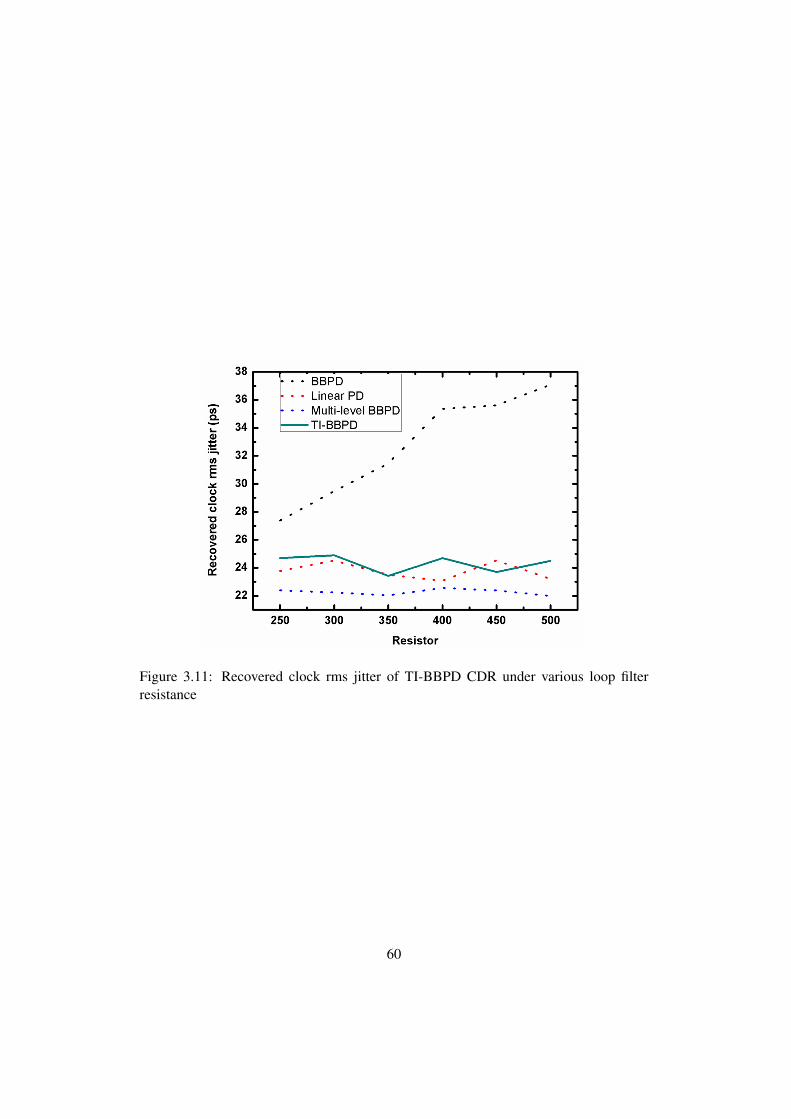
Figure 3.11: Recovered clock rms jitter of TI-BBPD CDR under various loop filterresistance
60

Figure 3.12: Loop dynamics variation of TI-BBPD CDR (a) PVT variation (b) Jitterdistribution
61

Figure 3.13: PD characteristic variation due to input data rate (a) Linear PD (b) BBPD(c) TI-BBPD
62

Linear PD BBPD ML-BBPD TI-BBPD
(Proposed)
PD characteristic Linear Non-linear Linear Linear
Loop filter sensitivity
(Variation rate (%)) 6% 40% 2% 6%
PVT sensitivity
(ωn Variation (MHz)) 2 MHz 7 MHz 3.5 MHz 2.8MHz
Jitter sensitivity
(ωn Variation (MHz)) 0.7 MHz 16.9 MHz 8.1 MHz 3.2MHz
Maximum speed (Gbps) 1 3 3 3
Power consumption (mW) 3.24 6.12 23.76 9.54
Power efficiency (mW/Gbps) 3.24 2.04 7.92 3.18
Table 3.1: Performance summary of TI-BBPD
63
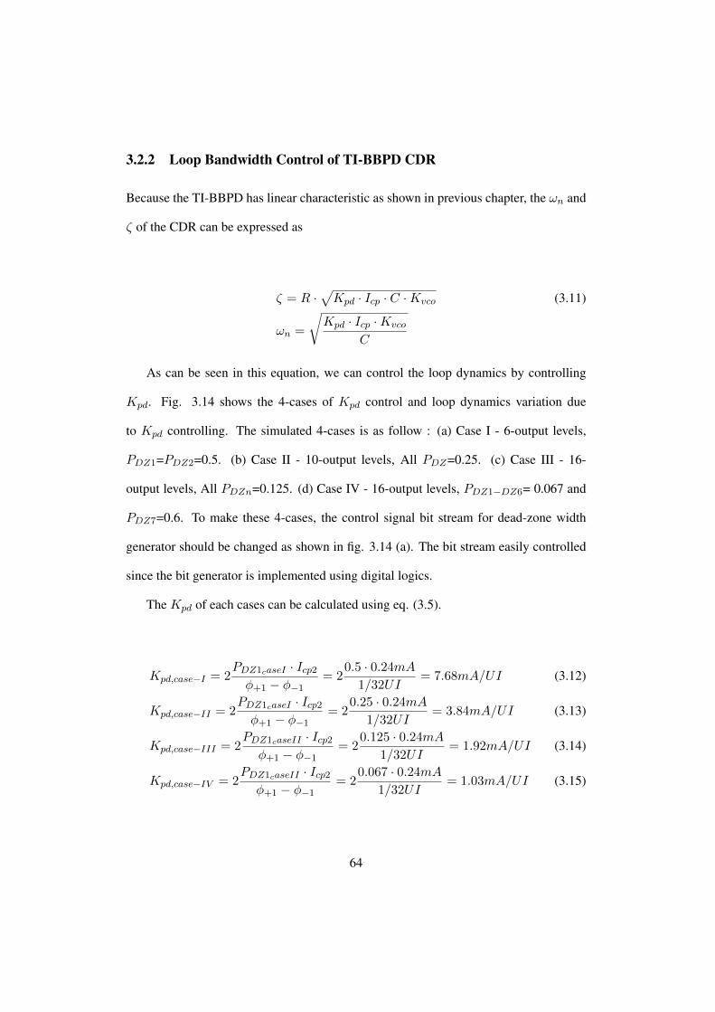
3.2.2 Loop Bandwidth Control of TI-BBPD CDR
Because the TI-BBPD has linear characteristic as shown in previous chapter, the ωn and
ζ of the CDR can be expressed as
ζ = R ·√Kpd · Icp · C ·Kvco (3.11)
ωn =
√Kpd · Icp ·Kvco
C
As can be seen in this equation, we can control the loop dynamics by controlling
Kpd. Fig. 3.14 shows the 4-cases of Kpd control and loop dynamics variation due
to Kpd controlling. The simulated 4-cases is as follow : (a) Case I - 6-output levels,
PDZ1=PDZ2=0.5. (b) Case II - 10-output levels, All PDZ=0.25. (c) Case III - 16-
output levels, All PDZn=0.125. (d) Case IV - 16-output levels, PDZ1−DZ6= 0.067 and
PDZ7=0.6. To make these 4-cases, the control signal bit stream for dead-zone width
generator should be changed as shown in fig. 3.14 (a). The bit stream easily controlled
since the bit generator is implemented using digital logics.
The Kpd of each cases can be calculated using eq. (3.5).
Kpd,case−I = 2PDZ1caseI · Icp2φ+1 − φ−1
= 20.5 · 0.24mA
1/32UI= 7.68mA/UI (3.12)
Kpd,case−II = 2PDZ1caseI · Icp2φ+1 − φ−1
= 20.25 · 0.24mA
1/32UI= 3.84mA/UI (3.13)
Kpd,case−III = 2PDZ1caseII · Icp2φ+1 − φ−1
= 20.125 · 0.24mA
1/32UI= 1.92mA/UI (3.14)
Kpd,case−IV = 2PDZ1caseII · Icp2φ+1 − φ−1
= 20.067 · 0.24mA
1/32UI= 1.03mA/UI (3.15)
64

where Icp2 = 0.24mA, and phase step of dead-zone width controller is 1/64UI. Fig.
3.14 (b) shows the loop dynamics simulation results under various Kpd case. For this
simulation, the rest design parameters such as Kvco, loop filter capacitance and resis-
tance are maintain constant for verifying Kpd effect on loop dynamics. The loop filter
capacitance C = 250pF, resistor R = 500 Ω are used in this simulation. A bit rate of
5Gbps is assumed and a randomly generated NRZ data stream with sinusoidal jitter is
fed to the CDR. As the frequency of the sinusoidal jitter is swept, the rms varations
of the applied input jitter and the resulting output jitter are recorded. The jitter transfer
characteristic is then calculated as the ratio between the input and output jitter variations.
As expected, when theKpd is reduced, the ωn also reduced. Simulated ωn where the
output jitter is reduced to half as compared to the input jitter is about 850MHz in case-I,
600MHz in case-II, 450MHz in case-III, and 300MHz in case-IV. These results shows
that the ωn is approximately proportional to square root of Kpd as expected.
65
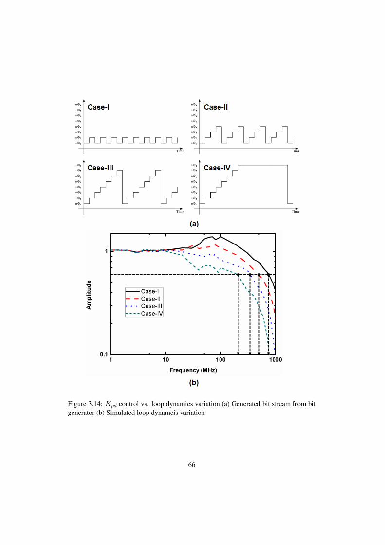
Figure 3.14: Kpd control vs. loop dynamics variation (a) Generated bit stream from bitgenerator (b) Simulated loop dynamcis variation
66

3.2.3 The Spur Reduction Techniques for TI-BBPD CDR
If the frequency of moving Icp is not sufficiently higher than ωn of TI-BBPD CDR,
undesired spur can arise in recovered clock. The spur is caused by periodic ripples on
the VCO control node due to periodically changed Icp. Since it can cause the timing
margin degradation, ωn of TI-BBPD CDR should be lower than the frequency of Icp. If
we assume that the bit generator generates stepwise dead-zone control bit as shown in
previous chapter, the maximum ωn of TI-BBPD CDR can be expressed as
ωn,max =fBG
2 · 2NBG(3.16)
where fBG is the operating frequency of bit generator, and NBG is the number of
output bit generated from bit generator. fBG is determined by the M-divided operating
frequency of TI-BBPD CDR. The frequency of moving Icp is determined by the number
of dead-zone and FBG. It should be at least 2 times higher than ωn of TI-BBPD CDR
to suppress the spur sufficiently. For example, the ωn,max of 1.25Gbps full-rate 18-level
TI-BBPD CDR shown in fig. 3.3 is about 2.437MHz if the fBG is 1.25/32 = 39MHz.
The simplest way to increase ωn,max is increasing the fBG. But the bit generator
has a speed limitation due to the silicon technology. Moreover, variable dead-zone gen-
erator which is commonly realized with digitally controlled phase interpolator can not
operate with too fast-changing control code. Thus, increasing fBG has a design-oriented
limitation.
Another possible solution for increasing ωn,max is that adding the DZPD and CP to
TI-BBPD as shown in fig. 3.15 (a). With this, we can rewrite the effective number of
67
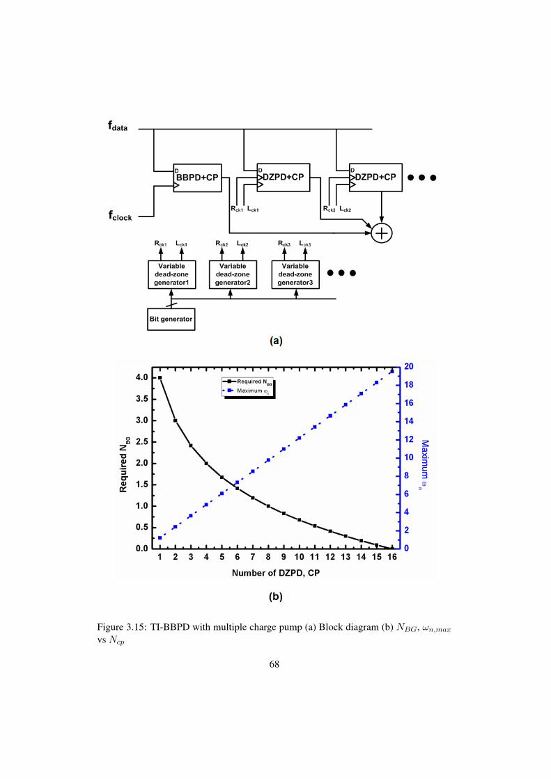
Figure 3.15: TI-BBPD with multiple charge pump (a) Block diagram (b) NBG, ωn,maxvs Ncp
68

TI-BBPD output levels as
Nlevel = 2 + 2 · 2NBG ·Ncp (3.17)
whereNcp is the number of DZPD and CP. If we add one more DZPD and CP, theNlevel
is increased linearly. In other words, we can reduce the NBG by adding the DZPD
and CP for achieving desired Nlevel. Fig. 3.15 (b) shows the ωn,max and NBG with
various Ncp for achieving 34-level TI-BBPD. We assume that the fBG is 39MHz, and
the operating frequency of CDR is 1.25Gbps. The ωn,max is increased if we use a large
number of additional DZPD and CP since required NBG is reduced.
Moreover, increasing Ncp can reduce the magnitude of spur itself. The magnitude of
spur is dominantly determined by the peak-to-peak value of dynamically changed Icp.
If we increase Ncp, it is possible to reduce the peak-to-peak value of Icp variation. For
example, if we dose not use DZPD and CP, then the Icp changes from +Icp to -Icp for
generating a certain level of Icp,avg. On the other hand, if Ncp is one, the Icp changes
from +Icp1 to +Icp2 for generating a same level of Icp,avg. Fig. 3.16 (a) shows the Icp
waveforms with each Ncp cases.
Although increasingNcp is attractive to enhance the performance of TI-BBPD CDR,
but the power consumption is directly proportional to Ncp. Briefly, if we use Ncp=16
for designing 34-level BBPD, the structure is identical to the conventional multi-level
BBPD. Fig. 3.16 (b) shows the spur and power consumption variation with various Ncp.
For easy calcultation, we assume that NBG is one, and the maximum Icp of each Ncp
case is same. The normalized power consumption is linearly increased withNcp, and the
spur is inversely proportional to Ncp as can be seen from the figure. The zero Ncp case
69
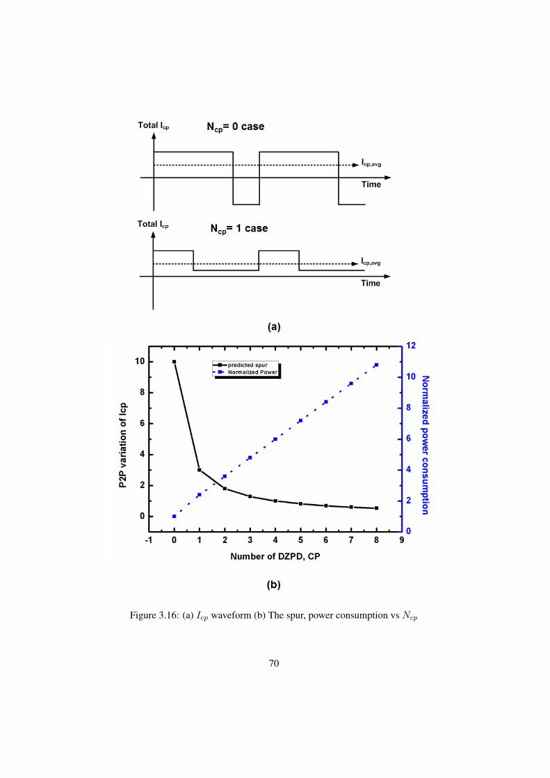
Figure 3.16: (a) Icp waveform (b) The spur, power consumption vs Ncp
70

means that the TI-BBPD without any DZPD and CP. The important point is that we dose
not need more than 2 or 3 additional DZPD and CP since its effect for spur reduction is
decreased. This is the reason that we use one DZPD and CP for designing TI-BBPD in
this paper.
The most sensible way to reduce the spur is generating non-periodic control bit for
dead-zone generator. Because the spur is comes from the periodic control bit, this solu-
tion blocks the spur completely. For this, we can use the high-order delta-sigma modula-
tor or PRBS pattern generator for generating control bit, instead of simple accumulator.
But it should be noted that generated control bits should have uniform distribution for
maintain the linear characteristic of TI-BBPD. Because the Icp,avg of a certain level is
determined by PDZ as shown in eq. (3.3), non-uniform distribution of control bits can
bring a changes to the difference between adjacent two levels. The high-order delta-
sigma modulator cannot satisfy this condition, and the PRBS pattern generator is also
periodic in a long-term view. The PRBS pattern generator which seed is changed by
high-order delta-sigma modulator may be used for control bit generation but its com-
plexity is not trivial. The method of non-periodic uniform-distributed bit generation
needs further research.
71

Chapter 4
On-Chip Jitter Monitoring
4.1 The Necessity of Signal Monitoring
Figure. 4.1 shows the roadmap of silicon manufacturing and test costs [31]. While the
manufacturing cost tends to be rapidly reduced, test cost has been maintained or slightly
increased. Also, while high-speed transceivers have been widely studied and reported,
the efforts to save test cost in this application are not enough.
A fundamental approach to check pass-fail of transmission system is to measure
BER of the output data of receiver. However, it takes a long time and requires expensive
equipment such as BER tester, resulting in the increase of test cost. On the other hand,
self-test method using on-chip signal monitoring circuit which plots the eye diagram or
jitter distribution of signal waveform inside the chip can be a powerful solution to reduce
the cost.
Moreover, the obtained information using signal monitoring circuit can give a intu-
ition to debuggers on operating status of the chips. For example, if we apply the mon-
itoring circuit to the CDR circuit, the CDR can directly check the input signal quality,
and the information about the input signal can be used for data sampling phase optimiza-
72
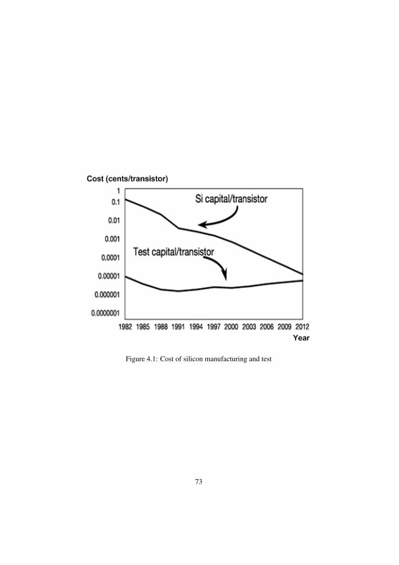
Figure 4.1: Cost of silicon manufacturing and test
73

tion or loop dynamics optimization. Because the signal monitoring circuit is possible to
observe the desired signal directly without being affected by PVT variation, it can be a
ultimate solution for designing a robust CDR. [19]-[21]
74

4.2 Signal Monitoring Circuit for CDR
The eye-opening monitoring (EOM) is one of widely used signal monitoring circuit.
A conventional EOM is composed of clocked-comparator, digital-to-analog converter
(DAC), phase controller, and digital processing block. [20] - [22] The block diagram
of classical EOM circuit with CDR is shown in fig. 4.2. The phase generator generates
sampling clock whose phase can be controlled by digital processing block. Since the
EOM circuit inherently needs accumulation process for obtaining correct signal quality
information, the phase generator generates one phase signal during a certain period.
Although parallel data sampling using multiple clock signal can reduce the total EOM
process time, it can significantly incease the hardware cost. The phase interpolator(PI)
or digital controlled delay line(DCDL) is commonly used for a phase generator, and
its resolution can determine the x-axis resolution of EOM results as shown in fig. 4.2
(b). The DAC generates reference voltages which are used for decision voltages of
comparators. Same as phase generator, the DAC also generates one reference voltage
during a certain period to reduce hardware cost of EOM. The Y-axis resolution in fig.
4.2 (b) can be deteremined by DAC resolution.
With phase generator and DAC, the comparator receives data desired to be observed
as input, and makes high or low output signal, which determines whether the input data
is larger or smaller than reference voltage from DAC at the rising edge of sampling
clock from the phase generator. The digital processing block accumlates the count of
comparator high output signals. After sufficient counting, the phase generator and DAC
changes their output to accumulate comparator output at another point in EOM. In this
75

DataΦdata
Φclock
Phase Detector
Charge Pump
Loop
filter
Voltage Controlled
Oscillator
Clock Tree
Digital processing
Phase controller
DAC
Eye opening monitoring
(a)
(b)
Y axis X axis
Figure 4.2: (a) Conventional structure of EOM (b) EOM result
76

manner, the EOM can get the input signal quality information.
However, the conventional EOM circuit has several drawbacks. First, it needs a
high-speed and high input sensitivity comparator. The comparator should detect the
small voltage difference between input voltage and reference voltage for obtaining a
accurate signal quality. Moreover, it should operate with high speed sampling clock for
reducing EOM processing time. Second, the phase generator and DAC should have high
resolution and constant phase or voltage step. To achieve these, a large number of control
bits and the thermometer-coded controller are required, and consequently, the hardware
complexity and chip area occupation are significantly increased.
In summary, the EOM can be a ultimate solution for the CDR performance enhance-
ment, but its design complexity is very high and hardware cost is not trival. To overcome
these problems, other signal monitoring circuit such as asynchronuous sampling EOM,
and jitter monitoring circuit can be used. A asynchronuous sampling EOM which does
not use the phase generator is reported in [22]. But it needs very long EOM processing
time and it is not suitable for CDR, whose timing information is very critical. Instead,
the jitter monitoring circuit which does not use the high-resolution DAC is more suitable
for the CDR. [23]-[25]
The jitter monitoring circuit can provide valuable information for CDR performance
when we assume that the equalizer compensates channel effect sufficiently because if the
input data stream does not suffer from ISI, jitter is the only thing that causes bit errors.
Moreover, jitter monitoring circuit is more suitable for low power signal monitoring de-
sign in comparison with EOM, since it does not need a high input sensitivity comparator
and high-resolution DAC. But most previously reported jitter monitoring circuits require
77
a reference clock [23]-[25], and consequently, cannot be used for the classical CDR
which does not receive the reference clock from a transmitter. Moreover, initial phase
difference between input data and sampling clock edges cannot be predicted in previous
works. Thus, the phase control range of a phase generator should cover more than one
UI and this can significantly increase the complexity of a phase generator especially in
high phase resolution case.
The jitter of received data means the phase difference between data and recovered
clock from CDR. Therefore, a jitter monitoring circuit for CDR, in principle, dose not
need additional circuits for jitter detection such as a high-speed comparator and phase
generator since the PD can detect the phase difference between data and VCO. Also,
if we use the PD as a jitter detection circuit, we don’t need a 1UI phase control range
due to unpredictable initial phase difference since the CDR feedback mechanism makes
the average phase difference between data and VCO as small as possible. But most
of previously reported jitter monitoring circuit have additional circuit for jitter detection
because both BBPD and hogge PD are not suitable for jitter detection circuit. The BBPD
does not distinguish the magnitude of phase error. Although the hogge PD can detect
the magnitude of phase error, but it is represented by pulse width which can not be
accumulated digitally. Although, some of previous works [32], [33] report the jitter
monitoring circuit using analog PD and time-to-digital converter (TDC), but the high-
resolution TDC comsumes large power and chip area. The multi-level BBPD can be
used for jitter detection circuit, but its hardware cost is very large itself.
78
4.3 On-Chip Jitter Monitoring Circuit using TI-BBPD
Using TI-BBPD, we can realize the jitter monitoring circuit without much hardware cost.
Because our TI-BBPD can produce the digitally represented phase error magnitude, we
can directly use the PD as a jitter detection circuit unlike BBPD, and Hogge PD.
The accumulated DZPD output can be used for generating jitter histograms since
DZPD output indicates the data transition is outside the DZPD dead-zone at the given
moment. Fig. 4.3 shows the block diagram of the jitter monitoring circuit using our
TI-BBPD. DZPD output signals are accumulated for each dead-zone width, resulting in
counters containing the number of data transitions (Cx) outside the dead-zone ranging
from -Φx to Φx. Then, the number of transitions in phase interval Φx to Φx+1 can be
easily determined by subtracting Cx+1 from Cx as can be seen from fig. 4.4. For the
phase interval 0 to Φ1, the number of transition can be obtained by subtracting C1 from
the maximum possible counter value C0.
The C0 can be derived as
C0 =Ctotal
4 · PDZ(4.1)
where Ctotal is the total number of sampled data transition. Because the transition prob-
ability is 0.5 and the probability of up signal is also 0.5, the Ctotal should be divide by 4.
Since Cx counts up only when the dead-zone is 2Φx, Ctotal should be divided by PDZx
for calculating C0. For example, if we design 18-level BBPD using proposed technique
and Ctotal is 65536, The C0 becomes 1024 when all PDZ is set to 1/8.
The proposed jitter monitoring has many advantages. First, thanks to CDR feed-
back mechanism, the complexity of phase generator can be significantly reduced since
79

the phase generator need not cover the one UI range . Second, the power comsumption
of jitter monitoring circuit can be significantly reduced as compared with conventional
ones. This can be achieved by the hardware sharing between the proposed jitter moni-
toring and CDR. They share the phase detector and phase generator, and consequently,
the jitter monitoring circuit dose not need a high-speed comparator and phase controller.
Third, the desing complexity of jitter monitoring circuit is alleviated. The only required
hardware for jitter monitoring circuit is an accumulator which can be synthesized with
standard cells.
80
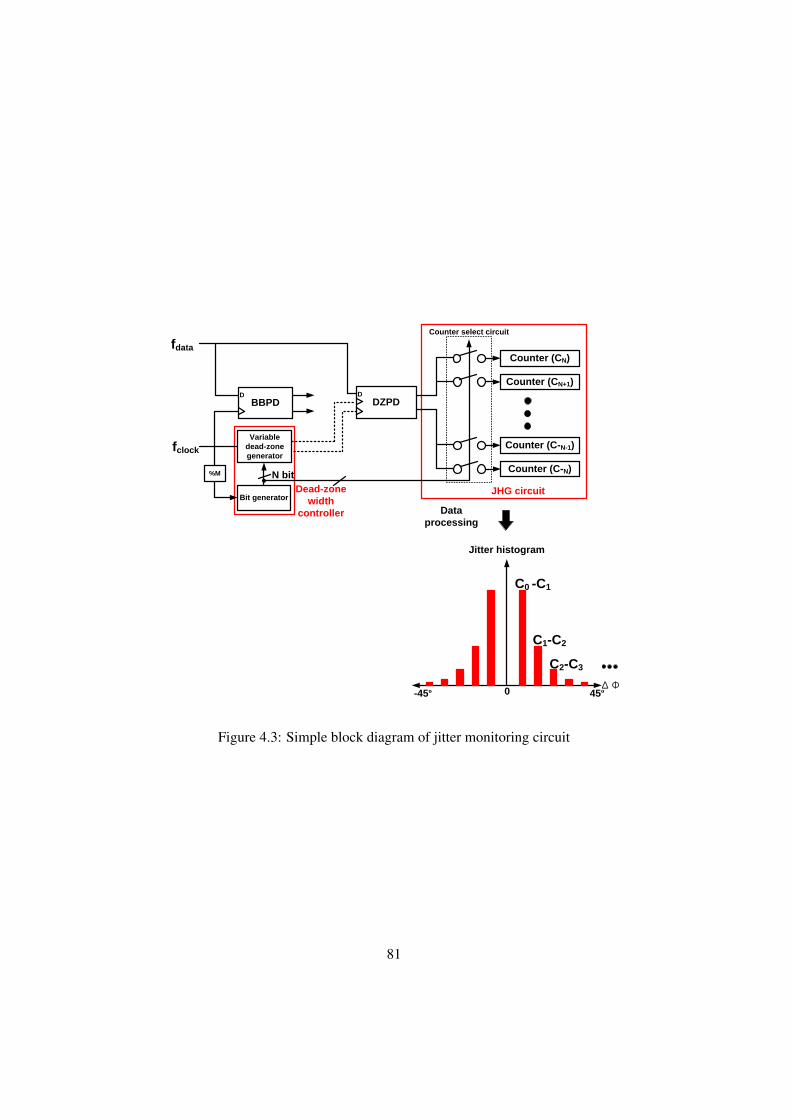
Δ Φ
C0 -C1
C1-C2
C2-C3
Jitter histogram
Data
processing
BBPD DZPDD D
fdata
fclock
%M
Variable
dead-zone
generator
Counter (CN)
Counter (CN+1)
Counter (C-N-1)
Counter (C-N)
Counter select circuit
JHG circuitBit generator
N bit
Dead-zone
width
controller
0 45º -45º
Figure 4.3: Simple block diagram of jitter monitoring circuit
81

Δ Φ
Δ Φ
CX+1
Jitter distribution Jitter distribution
Counter value Counter value
ΦX
CX
Δ Φ
0 ΦX+1Δ Φ
ΦX0 ΦX+1
ΦX0 ΦX+1 ΦX0 ΦX+1
Δ Φ
Jitter distribution
Jitter histogram
ΦX
CX – CX+1
Δ Φ
0 ΦX+1
ΦX ~ ΦX+1 0
45º -45º
45º -45º
45º -45º
45º -45º
45º -45º
45º -45º
Figure 4.4: Operational principle of jitter monitoring circuit
82
Chapter 5
Implementation
5.1 Overall Architecture
Fig. 5.1 shows the block diagram of our CDR circuit. An off-chip resistor and a capac-
itor are used for loop filter realization so that we can easily modify the loop dynamics
for evaluation purpose. Each of two identical phase interpolators has 3 control bits and
produces DZPD clock with 8 different phases in the opposite direction. Another PI with
a fixed control bit is used for generating BBPD clock. The bit generator (BG) scans
PI control bits producing sequentially changing 16 dead-zone widths for DZPD. Two
charge pumps with different Icp’s are connected to the same loop filter. The VCO is a
ring-type oscillator. The BG and jitter monitoring circuit (JM) is synthesized with stan-
dard cells. 1/32 frequency divider reduces the VCO clock for generating low-frequency
master clock of BG and JM.
5.2 TI-BBPD and CP
The TI-BBPD is composed of one DZPD and one BBPD as mentioned in previous chap-
ter. The BBPD contains 4 D-flipflops. 2 D-flipflops are used for the sampling input edge
83

Input
data
Bit generator
BBPD
DZPD
Jitter Monitoring
3 bit
Recovered clock
Recovered data
VCO I/Q
clock
Frequency
divider (1/32)
3 bit
Dead zone
width
controller
UP
DOWN
CP
(Icp2)
UP
DOWN
Ring
VCO
CP
(Icp1)
Off-chip
loop filter
PI
PI
PI
BBPD
clock
DZPD
clockDZPD
clock
Figure 5.1: Architecture of proposed CDR with jitter monitoring circuit
84

and data, and the rest is used for re-arranging the sampled data. The structure of DZPD
is completely same as BBPD. The only difference between BBPD and DZPD is ap-
plied clock phase. The sampling clocks of BBPD are 0 phase clock for data-sampling
and 180 phase clock for edge-sampling. By contrast, the DZPD needs two sampling
clock (Lclk, Rclk) whose phase is continuously changed around edge-sampling clock of
BBPD.
Fig. 5.2 (a) shows the whole block diagram of TI-BBPD. To reduce control voltage
ripple, the fanout of each D-flipflops which are connected to the XOR gate is adjusted as
same as possible. The D-flipflop which is a unit building block for TI-BBPD is realized
with sense-amplifier and two NAND gates as shown in fig. 5.2 (b). This sense amplifier
combines strong positive feedback with a high resistive input. The current flow of the
differential input transistors controls the serially connected latch circuit. A small differ-
ence between the currents through input transistors convertes to a large output voltage.
The D-flipflop based on sense amplifier has high input sensitivity by the benefit of the
latch operation of sense amplifier. However, the output signal of the sense amplifier is
RZ type, a NAND latch is required for conversion into NRZ.
The XOR gate is realized with only CMOS logics for reducing power consumption.
Because the charge pump has different type of switching MOS, we used XNOR gate for
generating ’late’ signal of BBPD and DZPD.
Each PD’s output is applied to two charge pumps whose current has different value.
In this design, we used 30 µA for BBPD which makes 1st level expected current. To
maintain a same difference between adjacent two current levels, we used 240 µA for
DZPD’s charge pump current in accordance with the eq. (3.6).
85

Input
data
0°
180°(Cclk)
179°(Lclk)
181°(Rclk)
360°
360°
360°
360°
UP
DOWN
CP
(Icp2)
UP
DOWN
CP
(Icp1)
DZPD
BBPD
(a)
Clk
Clk
INp
Clk
INn
OUTp OUTn
(b)
Figure 5.2: (a) Block diagram of TI-BBPD (b) D-flipflop structure
86

Vcpref
Vfeed
Vcpbias
UP
DOWN
Vcpbias
(a)
(b)
Vrep
Vcont
Mbias
Figure 5.3: (a) Charge pump structure (b) Charge pump bias circuit
87

As for the charge pump, we used a charge pump with the replica path in our design.
The block diagram of charge pump is shown in fig. 5.3 (a) [29]. Icp is determined by
Vcpbias, which is generated from the charge pump bias circuit. The output voltage of
the amplifier in the charge pump adaptively determines Vfeed in order to minimize the
charge pump mismatch currents under PVT and charge pump output voltage variation.
Fig. 5.3 (b) shows the charge pump bias circuit. The gate voltage of Mbias used for
Vcpbias is designed so that Vcpref and Vrep are equal to each other. Thus, we can control
Vcpbias by changing the Vcpref voltage or active load resistance. Each charge pumps
have different Vcpbias to generate the different Icp for TI-BBPD.
Although the maximum operating speed of this CP is relatively low as compared
with V-I converter which is commonly used for designing high-speed CDR, we used it
since our prototype chip focuses on verifying the linear characteristic of TI-BBPD CDR,
and JM system operation.
88

5.3 Voltage-Controlled Oscillator
Fig. 5.4(a) shows the schematics of the 2-stage pseudo-differential ring-type VCO with
lee-kim delay cell used in our design. The VCO has two control node, coarse tuning node
for frequency acquision and fine tuning node for phase acquision as shown in fig. 5.4
(b). A fine tuning node is connected to CDR loop and coarse tuning node is controlled
by externally supplied voltage. Both coarse tuning VCO gain and fine tuning VCO gain
can be determined by Mcoarse and Mfine, respectively. For our design, the oscillation
frequency of VCO can be changed from 1 GHz to 1.8GHz by controlling the coarse
tuning node voltage. This tuning range can satisfy the target frequency (1.25GHz) under
any process corner as shown in fig. 5.4 (c). A fine tuning VCO gain which is a important
parameter of CDR loop dynamics is about 200MHz/V determined by simulation.
The lee-kim delay cell has better phase noise performance compared to fully differ-
ential delay cell as explained in [34]. However, the VCO with lee-kim delay cell suffers
from duty cycle distortion. Because the full-rate CDR uses both rising and falling edge
of VCO clock for edge detection and data retiming, the duty cycle distortion can cause
timing margin reduction. To prevent this, our VCO used a feedforward type duty-cycle
corrector [30] as shown in fig. 5.5 (a). The duty-cycle corrector utilizes multiphase sig-
nals generated from a 2-stage different VCO. The signal inp in fig. 5.5 (a) selected from
the multiphase siganls turns on M1 and M2, and charges the output node DCCout of
the duty-cycle corrector almost instantaneously, because the discharge path of the node
DCCout is already off due to the signal inn. The signal inn, which is also selected from
the multiphase signals, is the one whose rising edge is shifted by 180 in phase from
89

that of inp. Similary, the signal inn rapidly discharges the node DCCout and delivers
the desired 50% duty-cycle signal. Since the duty-cycle correction circuit consists of
only two transmission gates and two inverters, the silicon area is minimal and the power
consumption is negligible. Fig. 5.5 (b) shows the waveform comparison between VCO
output and DCC output. The duty cycle of VCO waveform is about 0.37, while that of
DCC waveform is about 0.504.
90

VCO cell VCO cell
0°
180°
270°
90°
(a)
inp inn
outp outn
Vfine Vfine VCoarseVCoarse
(b)
(c)
MCoarse
Mfine Mfine
MCoarse
Target frequency = 1.25 GHz
Figure 5.4: (a) VCO structure (b) Lee-Kim delay cell (c) Clock duty-cycle corrector
91
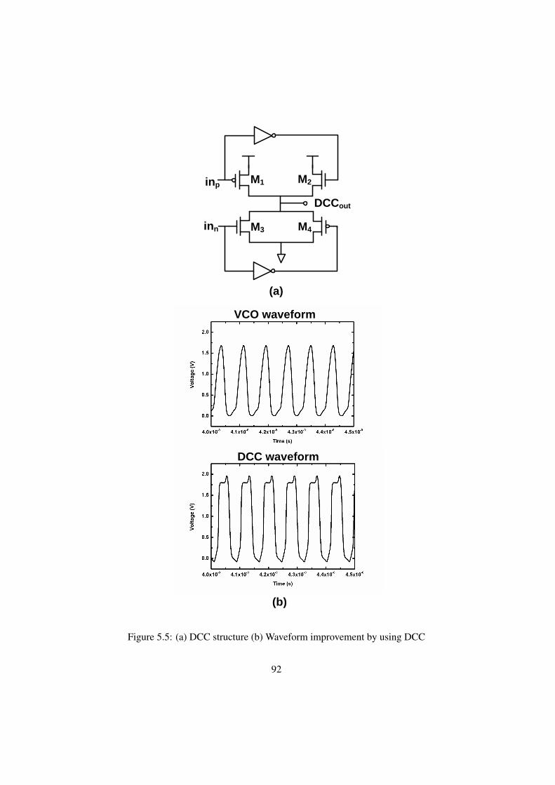
inn
inp
DCCout
M1 M2
M3 M4
(a)
(b)
VCO waveform
DCC waveform
Figure 5.5: (a) DCC structure (b) Waveform improvement by using DCC
92

5.4 Dead-Zone Width Controller
The dead-zone width controller is composed of 3-phase interpolators (PIs), bit generator
(BG) and frequency divider as shown in fig. 5.6 (a). The PI receives two clocks φ, ψ and
generates the main clock Θ whose phase is the weighted sum of the two input phases.
Essentially, the PI converts a digital weight code generated from BG to the phase of
clock Θ. The linearity and monotinicity of the PI is important in this design, since
it is related to the linearity of TI-BBPD. Additionally, the phase step is desired to be
minimize since the narrow phase step can make the jitter monitoring circuit having high
phase resolution. In our implementation, the interpolation step is 1/16 of the 90 inverval
resulting in approximately 5.6.
Fig. 5.6 (b) shows a schematic diagram of the interpolator used in the prototype chip.
This design is a dual input differential buffer which uses active load. For improving
the linearity of the PI, the current source of the two differential pairs is realized with
thermometer controlled elementes. The thermometer codes are generated from 3 bit
binary to thermomerter decoder. We used 3 identical PI to generate 3 clock phases. the
Lclk,Rclk, Cclk is for left end of dead-zone, right end of dead-zone, and BBPD sampling
clock, respectively. The PI for Rclk and Lclk are received same continously changed
digital weight code from BG. Since the input clock phase of PI for Lclk is reverse to that
of PI for Rclk, the output clock phases of each PIs are varied in the opposite direction.
The Cclk used for BBPD sampling clock is generated from the PI having constant digital
weight code.
The BG generates PI control signal. In this design, the output bit stream of BG have
93
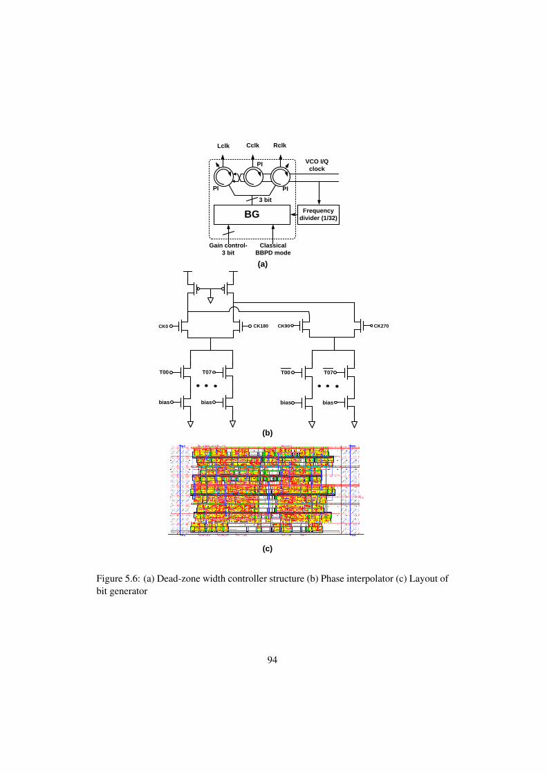
BG
VCO I/Q
clock
Frequency
divider (1/32)
3 bit
PI
PI
PI
Cclk RclkLclk
CK0
T00
bias
T07
bias
CK180 CK90 CK270
Gain control-
3 bit
Classical
BBPD mode
(a)
T00
bias
T07
bias
(b)
(c)
Figure 5.6: (a) Dead-zone width controller structure (b) Phase interpolator (c) Layout ofbit generator
94
stepwise form as shown previously. Since we can easily control the Kpd by changing
the ouptut bit stream as explained in chapter 3.2.2, the output bit stream can be changed
corresponding to 3-bit external control signal for evaluation purpose in this design. As
a result, the TI-BBPD have 8-different Kpd. The whole structure of BG is synthesized
with standard cells as shown in fig. 5.6 (c). Because of speed limitation of standard
cell, the BG need low-frequency master clock which is generated from 1/32 frequency
divider, resulting in 39.0625MHz clock signal.
95

5.5 Jitter Monitoring Circuit
The jitter monitoring (JM) circuit is composed of low-frequency sampler, counter select
circuit, 17-counters. The block diagram is shown in fig. 5.7. To achieve precise jitter
monitoring, the most important block is counter select circuit. The counter select cir-
cuit receives control code from BG, and decides the proper counter which accumulates
the current DZPD output signal. The timing mismatch between select signal from BG
and DZPD ouptut can cause the wrong decision of counter select circuit. For instance,
the DZPD output generated by ±φ1 dead-zone may be accumulated to Cφ2 counter be-
cause of the timing mismatch. But this problem is not important in this design, since the
counter accumulate the data transition which occurs outside of current dead-zone. Re-
sultingly, the counter having largest accumulation value must be the counter for smallest
dead-zone width (counter Cφ1).
The low frequency sampler is also used to slow down the DZPD output. 16-counters
accumulate the DZPD output and the clock counter for detecting total data transition is
added. To reduce output pin of prototype chip, outputs of each counters are connected
to the externally controlled MUX which can select the counter value desired to be mea-
sured. The whole structure is synthesized with standard cells. To operate these low speed
standard cells, 1/32-divided VCO clock is used same as BG.
96

UP
DOWN
Counter
select
Select signal
from bit
generator
Jitter Monitoring
Clock from
frequency
divider
Counter
select
M
U
X
counter (Ctotal)
counter (C-Φ1)
counter (C-Φ8)
counter (C-Φ2)
counter (CΦ1)
counter (CΦ2)
counter (CΦ8)
Figure 5.7: Block diagram of jitter monitoring circuit
97

Chapter 6
Experimental Results
A prototype chip is fabricated in 0.18 µm CMOS technology. Fig. 6.1 shows the chip
micrograph. The circuit consumes 39.6mW excluding output buffers with 1.8V supply
and its size is 0.12mm2. Each of BBPD and DZPD consumes 7.2mW, the dead-zone
width controller composed of PI, BG, and clock tree consumes 9.6mW. The charge pump
and VCO consumes 1.8mW and 10.8mW, respectively. In our design, the addtional
required power for JM is only 3mW. Although the area of JM is a little larger than other
blocks, it will be significantly reduced with more advanced CMOS technology. The TI-
BBPD has 18-level output. If we assume that the classical 18-level BBPD is designed
with same sub-blocks of our TI-BBPD, it probably consumes 7.2 × 18 = 129.6mW
which is even larger than the power consumption of the whole CDR.
Fig.6.2 shows the measurement setup for evaluating the CDR performance. The
chips are mounted on PCB with bonding-wires. The Pattern Pulse Generator (PPG) gen-
erate 1.25Gb/s 231-1 PRBS pattern for CDR input data. To measure the signal quality
of recovered clock and recovered data from our CDR, we used the spectrum analyzer
for measuring the frequency response of recovered clock frequency, and the digital sam-
98

Figure 6.1: Chip microphotograph
99

Figure 6.2: Measurement setup for evaluating the CDR performance
100

pling oscilloscope for measuring the eye diagram of recovered clock and data. Also Bit
Error Rate Tester (BERT) is used for measuring BER. To evaluate the jitter monitoring
capability, the Field-Programmable Gate Array (FPGA) board is used to receive the jitter
information from the JM in our chip. The received jitter information is send to the com-
puter to substrate adjacent counter values for obtaining jitter histogram. Since the input
data comes from the equipment for this measurement, we assume that the input data
doesn’t have jitter. Thus, the obtained jitter histogram from our chip is compared with
measured rms jitter histogram of recovered clock using digital sampling oscilloscope.
First of all, we measure the performance of VCO to check the operation frequency
range of CDR and process corner of the fabricated chip. Fig. 6.3 (a) shows the free-
running VCO spectrum at 1.25GHz oscillation frequency, and (b) shows the frequency
range of VCO with coarse control voltage tuning. For this measurement, the fine tuning
voltage is fixed to half-VDD value, and the coarse tuning voltage is controlled by external
voltage source. The VCO oscillation frequency range is shown in fig. 6.3 (b). The
process corner of the fabricated chip is approximately between Fast/Fast corner and
Normal/Normal corner.
The recovered clock spectrum and waveform is measured by the spectrum analyzer
and digital sampling oscilloscope, respectively. The measurement results are shown in
fig. 6.4. For this measurement, we used 1.25Gb/s 27-1 PRBS pattern as a input data. In
this case, the spectrum of recovered clock has spurs at interval of 5MHz as can be seen
from the fig. 6.4 (a). The reason for the 5MHz spur inverval is that the control voltage
ripple as explained in chapter 3.2.3. The ωn,max is about 2.5MHz since NBG is 3 and
fBG is 39MHz in our implementation, but the ωn in this measurement is about more than
101

Figure 6.3: Measurement results of free-running VCO (a) VCO spectrum @ 1.25GHz(b) Oscillation frequency range
102

Figure 6.4: Measurement of CDR recovered clock (a) Spectrum (b) Waveform
103

5MHz, the CDR can not sufficiently suppress the spur. We also abserved that the spur
is reduced when the input data stream is changed to 231-1 PRBS pattern. We believe
that this is because the periodicity of the control voltage ripple is weakened slightly by
complex input signal. The recovered clock waveform is shown in fig. 6.4 (b). The rms
jitter of the clock signal is about 4ps (0.0054UI) as shown in the figure.
The eye diagram of retimed data is shown in fig. 6.5 (a). For this measurement, the
1.25Gb/s 231-1 PRBS pattern is used. The rms jitter of retimed data is almost same as
that of recovered clock. the BER is error-free (under 10−12) as can be seen from the fig.
6.5 (b).
In order to evaluate gain linearization of our TI-BBPD, the influence of varing loop-
filter characteristics on the recovered clock jitter is measured for 2-level BBPD and 18-
level TI-BBPD. 2-level BBPD is realized with the same circuit by fixing the DZPD
dead-zone width to zero. The CDR having linear loop dynamics characteristic should
have much more robust recover clock jitter performance against loop filter characteristic
since it does not suffer from BBPD nonlinearity as explained in chapter 3.2.1. Fig. 6.6
shows the measured rms jitters of recovered clocks for two cases with various R and C
values used in the loop filter. For both, input data are 1.25Gb/s 231-1 PRBS pattern. The
recovered clock rms jitter changes widely from 4ps to 37ps depending on R, C values
for 2-level BBPD CDR, but it remains under 8ps with very little deviation for 18-level
TI-BBPD. This confirms that our TI-BBPD has the multi-level, linear characteristics.
In addition, the result is the proof of PVT immunity of TI-BBPD CDR because the the
effect of various R, C values for CDR can be substitute for that of PVT variation.
Our TI-BBPD can control its gain by changing the PDZn as can be seen from the
104

Figure 6.5: Measurement of CDR recovered data (a) Eye-diagram (b) BER
105

Figure 6.6: Measured recovered clock rms jitter (a) 2-level BBPD CDR (b) 18-levelTI-BBPD CDR
106

fig. 3.14. The measurement results of the recovered clock spectrum with various Kpd
is shown in fig. 6.7. With the clock spectrum measurement results, we can roughly
estimate the ωn. For example, in the case of 2-level BBPD shown in fig. 6.7 (a), the ωn
is about 25MHz. We can observe that the 2-level BBPD CDR has relatively large ωn due
to the largeKpd. Fig. 6.7 (b),(c),(d) shows the recovered clock spectrum variation due to
the decrease ofKpd, sequentially. To control theKpd of our TI-BBPD, the BG generates
different output bit stream for each cases as shown in the figure. The normalized Kpd of
(b), (c), and (d) is 1, 0.5, and 0.28, respectively. As expected, we can observe that the
roughly estimated ωn is decreased corresponding to the Kpd. The ωn of (b), (c), and (d)
is observed as 15MHz, 10MHz, and 7MHz, respectively. The results are well matched
to the eq.(3.12). The frequency interval of spur is decreased corresponding to the output
bit stream as expected. These measurement results confirm that the Kpd of TI-BBPD
becomes a easily controllable design parameter unlike the classical BBPD which gain is
determined by environmental condition.
Fig. 6.8 shows the oscilloscope-measured recovered clock jitter distributions at four
different loop filter R, C values and the jitter histograms obtained by our circuit. The
input data is again 1.25Gb/s 231-1 PRBS pattern. The Ctotal is 32768, and the C0 is
1024 in accordance with eq.(4.1). Each phase step has about 13ps corresponding to
1/64 UI. The JM circuit produce correct jitter distributions. If the recovered clock rms
jitter becomes larger, the jitter monitoring output is also changed to have smaller peak
histogram value and the data transition is appeared at the phase slot which is more far
from the Φ0. The slight non-symmetricity observed in the jitter histograms is believed
due to mismatch among three PIs in our circuit.
107
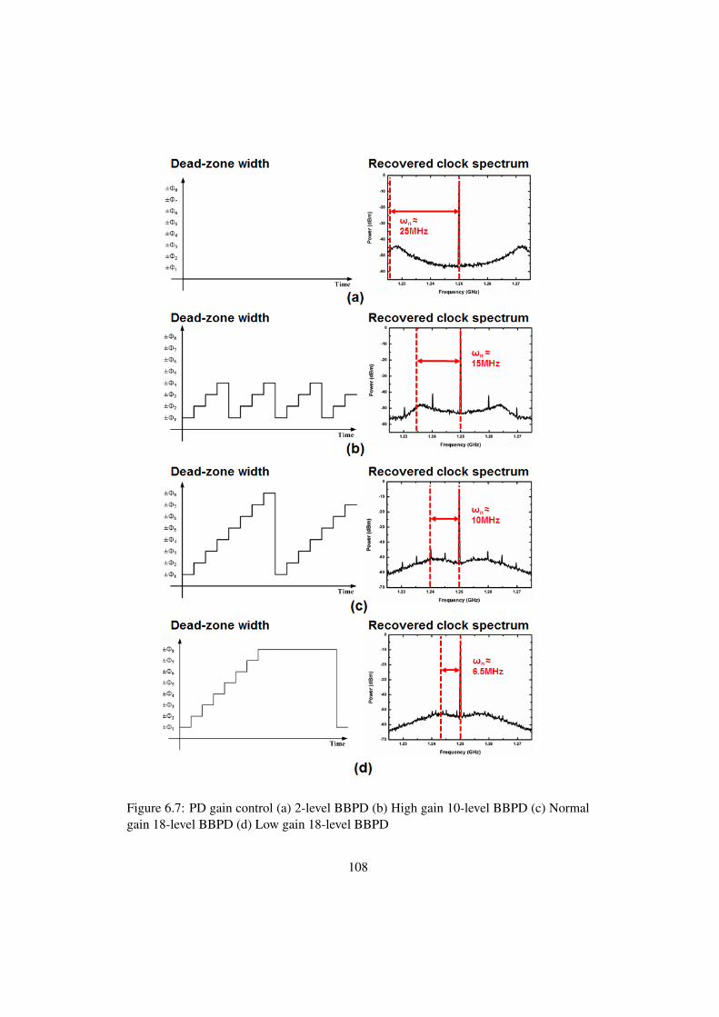
Figure 6.7: PD gain control (a) 2-level BBPD (b) High gain 10-level BBPD (c) Normalgain 18-level BBPD (d) Low gain 18-level BBPD
108

Figure 6.8: Measured rms jitter of recovered clock and jitter monitoring output
109

Chapter 7
Summary
Since the CDR is a essential block for designing serial-link I/O transceiver, a high-speed,
low-power, robust CDR design is highly desired. To achieve that, the PD plays an im-
portant role, but previously reported PD structures are not able to satisfy all the desired
performances. The linear PD has a speed limitation, the BBPD is very sensitive to the
environment condition, and the multi-level BBPD comsumes large power.
In this paper, we propose a novel multi-level BBPD structure, whose hardware cost is
drastically reduced as compared with the conventional multi-level BBPD. By applying
time-interleaving method to BBPD, our TI-BBPD can have a large number of output
levels without worring about the hardware cost. Thanks to its linear characteristic, we
can design a robust CDR and also, we can analyze the CDR with well-known linear
analysis. Futhermore, we can change the ωn by using completely digital control. This
function could be a very useful, if it combines with jitter monitoring capability which is
another benefit provided by our TI-BBPD.
The prototype chip is fabricated with 0.18 µm CMOS technology. The overall CDR
architecture achieves linear characteristic, and consequently, it has a robust performance
110
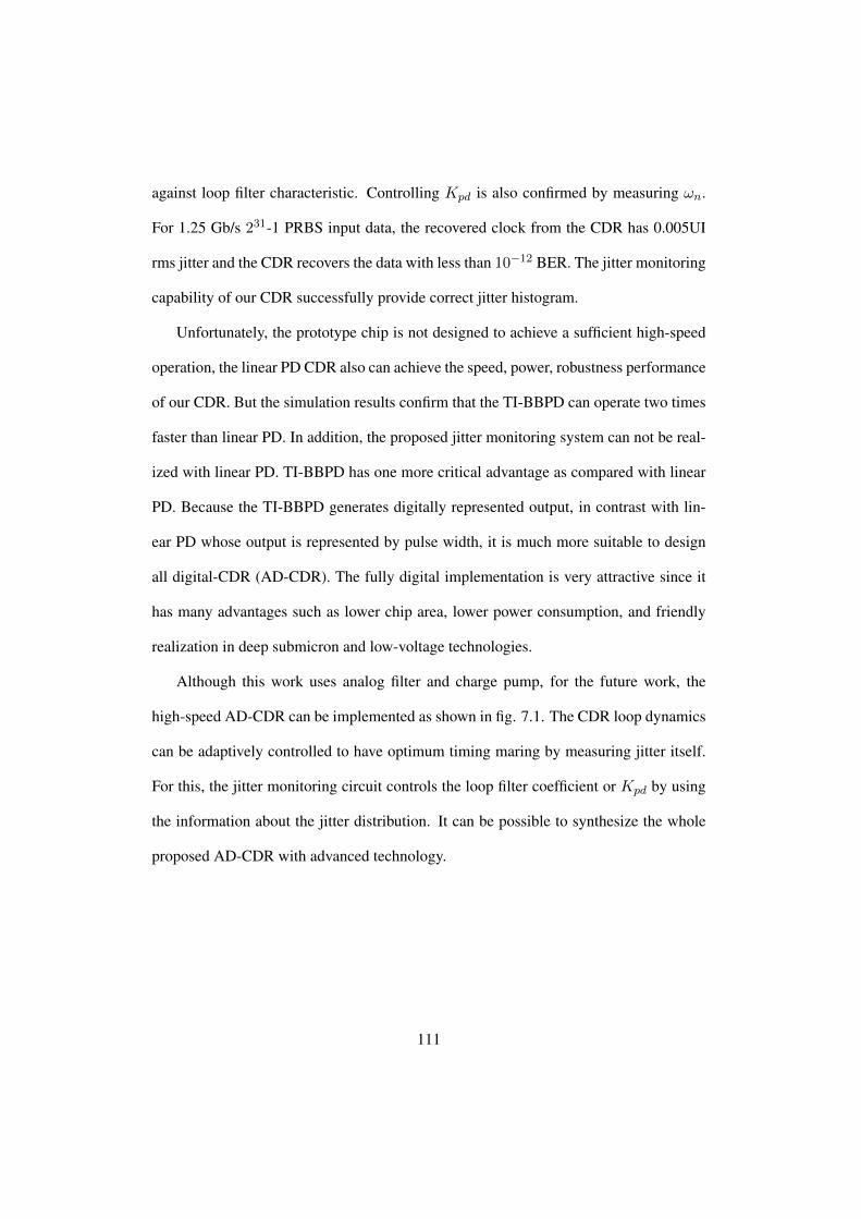
against loop filter characteristic. Controlling Kpd is also confirmed by measuring ωn.
For 1.25 Gb/s 231-1 PRBS input data, the recovered clock from the CDR has 0.005UI
rms jitter and the CDR recovers the data with less than 10−12 BER. The jitter monitoring
capability of our CDR successfully provide correct jitter histogram.
Unfortunately, the prototype chip is not designed to achieve a sufficient high-speed
operation, the linear PD CDR also can achieve the speed, power, robustness performance
of our CDR. But the simulation results confirm that the TI-BBPD can operate two times
faster than linear PD. In addition, the proposed jitter monitoring system can not be real-
ized with linear PD. TI-BBPD has one more critical advantage as compared with linear
PD. Because the TI-BBPD generates digitally represented output, in contrast with lin-
ear PD whose output is represented by pulse width, it is much more suitable to design
all digital-CDR (AD-CDR). The fully digital implementation is very attractive since it
has many advantages such as lower chip area, lower power consumption, and friendly
realization in deep submicron and low-voltage technologies.
Although this work uses analog filter and charge pump, for the future work, the
high-speed AD-CDR can be implemented as shown in fig. 7.1. The CDR loop dynamics
can be adaptively controlled to have optimum timing maring by measuring jitter itself.
For this, the jitter monitoring circuit controls the loop filter coefficient or Kpd by using
the information about the jitter distribution. It can be possible to synthesize the whole
proposed AD-CDR with advanced technology.
111
Input
data
Recovered clockRecovered data
DCO
TI-BBPD Digital Filter
Dead-zone
width controller
Jitter monitoring circuit
JM inputCounter select
Gain control
Filter coefficient
control
Figure 7.1: Simple block diagram of ADCDR with jitter monitoring circuit
112

Appendix
High-speed CDR design with advanced CMOS technology
We can design CDR having much higher operating speed with advanced CMOS technol-
ogy and multi-phase clock. Fig. A.1 shows the whole block diagram of 25Gbps-CDR
with 65nm CMOS technology. In this design, we dose not use additional DZPD and CP
since the input load capacitance becomes a critical issue for designing high speed appli-
cation. For generating linear characteristic of BBPD, the edge sampling clock phase is
continuously changed by digitally controlled phase interpolator and the data sampling
clock whose phase should be placed at the middle of edge sampling clocks is generated
by identical phase interpolator whose digital code is fixed.
Fig. A.2 shows the simulation results. In this simulation, we assume that the VCO
and CP can operate with sufficiently high frequency, thus, the VCO and CP is coded with
Verilog-A language. As can be seen from the figures, the CDR locking voltage is stably
settled at 0.9V, and 25Gbps data is successfully recovered without error. After CDR
locking, the proposed CDR have a long term dithering as compared with conventional
BBPD CDR as expected. The linear characteristic of proposed PD is also shown in the
figure. Generally, since the transistor-level circuit simulation can guarantee 50% oper-
113

D Q
D Q
0° Clock
70°~110° Clock
D Q
D Q
180° Clock
250°~290° Clock
Bit control
7-signal
CP
CP
70°~110°
Clock
250°~290°
Clock
0°
Clock
180°
Clock
Figure A.1: Block diagram of 25Gbps CDR with 65nm CMOS technology
ating speed of fabricated circuit, the designed CDR can probably be used for 12.5Gbps
data transmission.
114
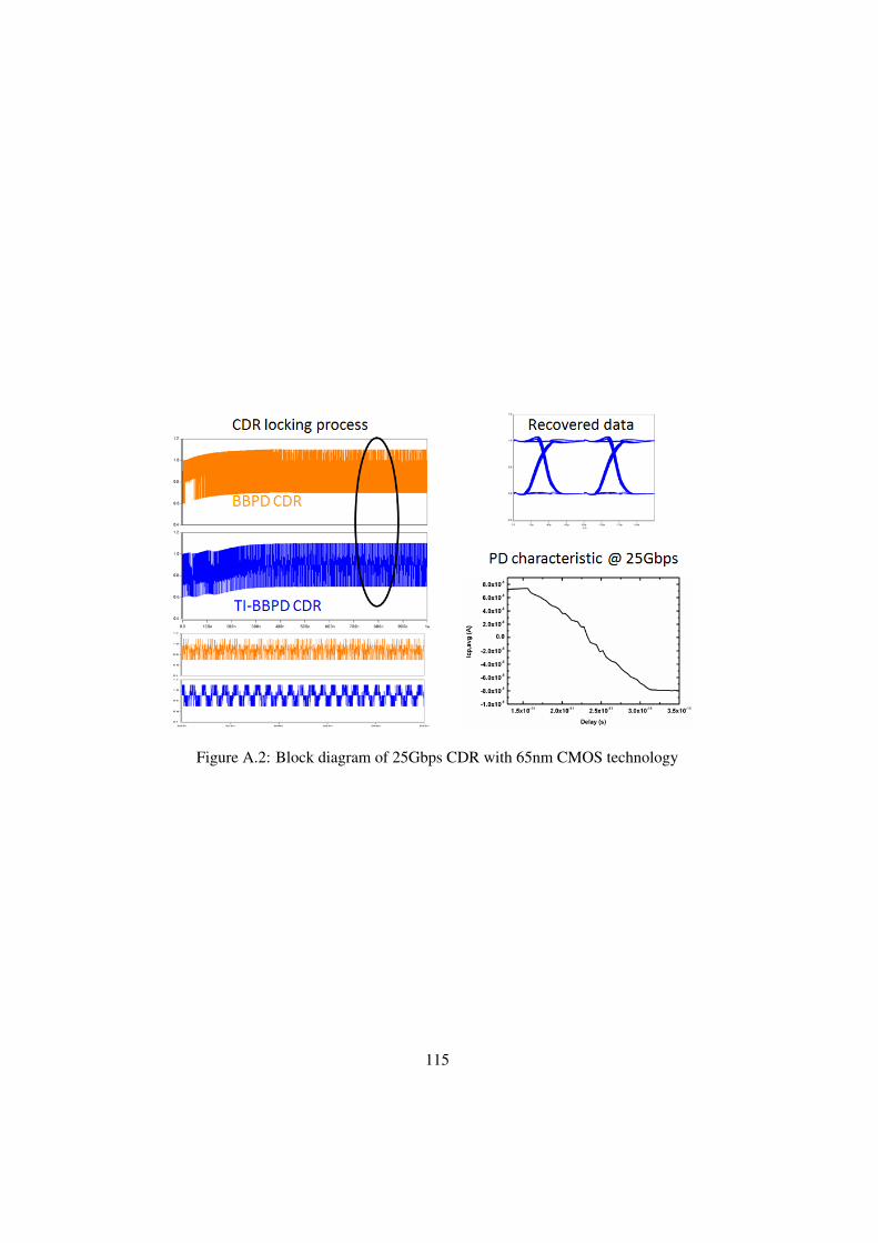
Figure A.2: Block diagram of 25Gbps CDR with 65nm CMOS technology
115

References
[1] R. C. Walker, “Designing Bang-Bang PLLs for Clock and Data Recovery in Serial
Data Transmission Systems,” Phase-Locking in High-Performance Systems, pp.34-
45, 2003
[2] N. D. Dalt, “A Design-Oriented Study of the Nonlinear Dynamics of Digital Bang-
Bang PLLs,” IEEE Trans. Circuits and Systmes-I, vol. 52, no. 1, pp.21-31, Jan.
2005
[3] N. D. Dalt, “Markov Chains-Based Derivation of the Phase Detector Gain in Bang-
Bang PLLs,” IEEE Trans. Circuits and Systmes-II, vol. 53, no. 11, pp.1195-1199,
Nov. 2006
[4] J. Lee, “Analysis and Modeling of Bang-Bang Clock and Data Recovery Circuits,”
IEEE J. Solid-State Circuits, vol. 39, no. 9, pp.1571-1580, Sep. 2004
[5] Y. D. Choi, D. K. Jeong, and W. C. Kim, “Jitter Transfer Analysis of Tracked
Oversampling Techniques for Multigigabit Clock and Data Recovery,” IEEE Trans.
Circuits and Systmes-II, vol. 50, no. 11, pp.775 - 783, Nov. 2003
116

[6] F. M. Gardner, “Charge-Pump Phase-Locked Loops,” IEEE Trans. on communi-
cations, vol. 28, no. 11, pp.1849-1858, Nov. 1980
[7] M. Ramezani, and A.T. Salama, “An Improved Bang-bang Phase Detector for
Clock and Data Recovery Applications,” IEEE International Symposiums on Cir-
cuits and Systems, pp. 715 - 718, Nov. 2001
[8] X. Chen, and M. M. Green, “A CMOS 10Gb/s Clock and Data Recovery Circuit
with A Novel Adjustable Kpd Phase Detector,” IEEE International Symposiums
on Circuits and Systems, pp. 301 - 304, Nov. 2004
[9] J. C. Zhuang, and T. Kwasniewski, “A Multi-level Phase/Frequency Detector For
Clock and Data Recovery Applications,” IEEE Canadian Conference on Electrical
and Computer Engineering, pp.828 - 830, May. 2005
[10] M. H. Perrott, et al., “A 2.5-Gb/s Multi-Rate 0.25-µm CMOS Clock and Data
Recovery Circuit Utilizing a Hybrid Analog/Digital Loop Filter and All-Digital
Referenceless Frequency Acquisition,” IEEE J. Solid-State Circuits, vol. 41, No.
12, pp.2930 - 2944, Dec. 2006
[11] N. Nedovic, et al., “A 40-44 Gb/s 3 × Oversampling CMOS CDR/1:16 DEMUX,”
IEEE J. Solid-State Circuits, vol. 42, No. 12, pp.2726 - 2735, Dec. 2007
[12] S. H. Lin, and S. I. Liu, “Full-Rate Bang-Bang Phase/Frequency Detectors for
Unilateral Continuous-Rate CDRs,” IEEE Trans. Circuits and Systmes-II, vol. 55,
no. 12, pp.1214 - 1218, Dec. 2003
117

[13] C. S-Azqueta, and S. Celma “A Phase Detection Scheme for Clock and Data Re-
covery Applications,” 20th European Conference on Circuit Theory and Design,
pp.130 - 133, Aug. 2011
[14] W. Yin, et al., “A TDC-Less 7mW 2.5Gb/s Digital CDR with Linear Loop Dynam-
ics and Offset-Free Data Recovery,” IEEE J. Solid-State Circuits, vol. 46, No. 12,
pp.3163 - 3173, Dec. 2011
[15] Y. L. Lee, et al., “A 5Gb/s 1/4-rate Clock and Data Recovery Circuit Using Dy-
namic Stepwise Bang-Bang Phase Detector,” IEEE Asian Solid-State Circuit Con-
ference, pp.141 - 144, Nov. 2012
[16] C. S-Azqueta, and S. Celma., “A Multi-Level Phase Detector in 90nm CMOS,”
IEEE Latin American Symposium on Circuits and Systems, pp.1 - 4, Mar. 2012
[17] R. Nonis, et al., “A 2.4psrms−jitter Digital PLL with Multi-Output Bang-Bang
Phase Detector and Phase-Interpolator-Based Fractional-N Divider,” ISSCC Deg.
Tech. Papers, pp.356 - 357, Feb. 2013
[18] H. J .Jeon, et al., “A Bang-Bang Clock and Data Recovery Using Mixed Mode
Adaptive Loop Gain Strategy,” IEEE J. Solid-State Circuits, vol. 48, No. 6, pp.1398
- 1415, Jun. 2013
[19] H. Noguchi, et al., “A 40-Gb/s CDR Circuit With Adaptive Decision-Point Control
Based on Eye-Opening Monitor Feedback,” IEEE J. Solid-State Circuits, vol. 43,
No. 12, pp.2929 - 2938, Dec. 2008
118
[20] T. Suttorp and U. Langmann, “A 10-Gb/s CMOS Serial-Link Receiver using Eye-
Opening Monitoring For Adaptive Equalization and for Clock and Data Recovery,”
IEEE Custom Integrated Circuits Conference, pp.277- 280, Sep. 2007
[21] C. K. Seong, et al., “A 10-Gb/s Adaptive Look-Ahead Decision Feedback Equal-
izer with an Eye-Opening Monitor,” IEEE Trans. Circuits and Systmes-II, vol. 59,
No. 4, pp. 209 - 213, Apr. 2012
[22] W. S. Kim, et al., “A 5.4-Gb/s Adaptive Continuous-Time Linear Equalizer Using
Asynchronous Under-Sampling Histogram,” IEEE Trans. Circuits and Systmes-II,
vol. 59, No. 9, pp. 553 - 556, Sep. 2012
[23] T. Hashimoto, et al., “Time-to-Digital Converter with Vernier Delay Mismatch
Compensation for High Resolution On-Die Clock Jitter Measurement,” IEEE Sym-
posium on VLSI Circuits, pp.166 - 167, Jun. 2008
[24] M. Sasaki, et al., “A Circuit for On-chip Skew Adjustment with Jitter and Setup
Time Measurement,” IEEE Asian Solid-State Circuit Conference, pp.1 - 4, Nov.
2010
[25] K. H. Cheng, et al., “Built-in Jitter Measurement Circuit with Calibration Tech-
niques for a 3-GHz Clock Generator,” IEEE Trans. Very Large Scale Integration
Systems, vol. 19, No. 8, pp.1325 - 1335, Aug. 2011
[26] Y. S. Moon, et al., “A 0.6-2.5 GBaud CMOS Tracked 3 × Oversampling
Transceiver with Dead-Zone Phase Detection for Robust Clock/Data Recovery,”
IEEE J. Solid-State Circuits, vol. 36, No. 12, pp.1974 - 1983, Dec. 2001
119

[27] S. H. Lee, et al., “A 5-Gb/s 0.25-µm CMOS Jitter-Tolerant Variable-Interval Over-
sampling Clock/Data Recovery Circuit,” IEEE J. Solid-State Circuits, vol. 37, No.
12, pp.1822 - 1830, Dec. 2002
[28] B. J. Lee, et al., “A 2.5-10 Gb/s CMOS Transceiver with Alternating Edge-
Sampling Phase Detection for Loop Characteristic Stabilization,” IEEE J. Solid-
State Circuits, vol. 38, No. 11, pp.1821 - 1829, Nov. 2003
[29] J. S. Lee, et al., “Charge pump with perfect current matching characteristics in
phase-locked loops,” IET Electronics Letters, vol. 36, No. 23, pp.1907 - 1908,
Nov. 2000
[30] J. S. Lee and B. S. Kim., “A Low-Noise Fast-Lock Phase-Locked Loop with Adap-
tive Bandwidth Control,” IEEE J. Solid-State Circuits, vol. 35, No. 8, pp.1137 -
1145, Nov. 2000
[31] L. T. Wang, et al., System-on-chip test architectures: nanometer design for testa-
bility, Elsevier, Burlington, MA, 2008
[32] J. M. Cazeaux, et al., “Novel On-Chip Circuit for Jitter Testing in High-Speed
PLLs,” IEEE Trans. on Instrumentation and Measurement, vol. 54, No. 5, pp.1779
- 1788, Oct. 2005
[33] J. Yu, and F. F. Dai, “On-chip Jitter Measurement Using Vernier Ring Time-to-
digital Converter,” IEEE Asian Test Symposium, pp. 167 -170 Oct. 2010
[34] V. Kratyuk, et al., “Analysis of Supply and Ground Noise Sensitivity in Ring and
120

LC Oscillators,” IEEE International Symposiums on Circuits and Systems, pp.
5986 - 5989, Nov. 2005
121

국 문 요 약
새로운 구조의 다중레벨 뱅뱅 위상 검출기를 사용한 클럭 엔
데이터 복원회로
클럭 엔 데이터 복원회로는 수신기 설계에 있어 매우 중요한 역할을 담당하고 있다. 따
라서 높은 동작속도, 낮은 전력소모, 그리고 환경에 둔감한 클럭 엔 데이터 복원회로의 설계
는 오래전부터 연구가 되어왔다.
본 논문은 새로운 구조의 다중레벨 뱅뱅 위상 검출기를 사용하여 높은 주파수로 동작하
면서도 환경에 매우 둔감할 수 있는 클럭 엔 데이터 복원회로를 제안하였다. 보통 높은 주
파수에서 동작하는 클럭 엔 데이터의 설계를 위해서는 뱅뱅 위상 검출기가 많이 사용되는
데, 이는 환경변수에 매우 민감한 비선형적인 특성을 가진다. 이를 극복하기 위해서 연구가
되어온 다중레벨 뱅뱅 위상 검출기의 경우 많은 면적과 전력을 소모한다는 단점이 있다. 본
구조는 하드웨어를 공유하고 다시 사용하는 방법으로 크게 추가되는 하드웨어 없이 뱅뱅 위
상 검출기의 특성을 선형화 하였으며, 추가적으로 선형화된 뱅뱅 위상검출기의 출력을 이용
한 지터 감지회로도 설계가 되었다.
180nm 공정을 사용하여 칩을 제작하였으며, 위상 검출기의 선형적 특성, 그리고 환경에
둔감한 특성, 지터 감지특성 모두가 성공적으로 동작하는 것을 실험을 통해 확인하였다. 또
한 1.25Gbps 231-1 PRBS 입력에 대해서 안정적으로 동작하며 복원된 클럭은 0.005UI 의
rms 지터 성능을 가지는 것을 확인하였다. 복원된 데이터 또한 에러가 없음을 확인하였다.
핵심되는 말 : 다중 레벨 뱅뱅 위상 검출기, 지터 감지회로, 클럭 엔 데이터 복원회로