DESIGN OF CLOCK DATA RECOVERY INTEGRATED CIRCUIT FOR HIGH SPEED
183
DESIGN OF CLOCK DATA RECOVERY INTEGRATED CIRCUIT FOR HIGH SPEED DATA COMMUNICATION SYSTEMS A Dissertation by JINGHHUA LI Submitted to the Office of Graduate Studies of Texas A&M University in partial fulfillment of the requirements for the degree of DOCTOR OF PHILOSOPHY December 2008 Major Subject: Electrical Engineering
Transcript of DESIGN OF CLOCK DATA RECOVERY INTEGRATED CIRCUIT FOR HIGH SPEED

DESIGN OF CLOCK DATA RECOVERY INTEGRATED CIRCUIT FOR HIGH
SPEED DATA COMMUNICATION SYSTEMS
A Dissertation
by
JINGHHUA LI
Submitted to the Office of Graduate Studies of Texas A&M University
in partial fulfillment of the requirements for the degree of
DOCTOR OF PHILOSOPHY
December 2008
Major Subject: Electrical Engineering

DESIGN OF CLOCK DATA RECOVERY INTEGRATED CIRCUIT FOR HIGH
SPEED DATA COMMUNICATION SYSTEMS
A Dissertation
by
JINGHUA LI
Submitted to the Office of Graduate Studies of Texas A&M University
in partial fulfillment of the requirements for the degree of
DOCTOR OF PHILOSOPHY
Approved by:
Chair of Committee, Jose Silva-Martinez Committee Members, Edgar Sanchez-Sinencio Weiping Shi Hongbin Zhan Head of Department, Costas N. Georghiades
December 2008
Major Subject: Electrical Engineering

iii
ABSTRACT
Design of Clock Data Recovery Integrated Circuit for High Speed Data Communication
Systems.
(December 2008)
Jinghua Li, B.S., Harbin Engineering University; M.S., Shanghai Jiaotong University
Chair of Advisory Committee: Dr. Jose Silva-Martinez
Demand for low cost Serializer and De-serializer (SerDes) integrated circuits has
increased due to the widespread use of Synchronous Optical Network (SONET)/Gigabit
Ethernet network and chip-to-chip interfaces such as PCI-Express (PCIe), Serial
ATA(SATA) and Fibre channel standard applications. Among all these applications,
clock data recovery (CDR) is one of the key design components. With the increasing
demand for higher bandwidth and high integration, Complementary metal-oxide-
semiconductor (CMOS) implementation is now a design trend for the predominant
products.
In this research work, a fully integrated 10Gb/s (OC-192) CDR architecture in
standard 0.18µm CMOS is developed. The proposed architecture integrates the typically
large off-chip filter capacitor by using two feed-forward paths configuration to generate
the required zero and poles and satisfies SONET jitter requirements with a total power
dissipation (including the buffers) of 290mW. The chip exceeds SONET OC-192 jitter
tolerance mask, and high frequency jitter tolerance is over 0.31 UIpp by applying PRBS
iv
data with a pattern length of 231-1.The implementation is the first fully integrated 10Gb/s
CDR IC which meets/exceeds the SONET standard in the literature.
The second proposed CDR architecture includes an adaptive bang-bang control
algorithm. For 6MHz sinusoidal jitter modulation, the new architecture reduces the
tracking error to 11.4ps peak-to-peak, versus that of 19.7ps of the conventional bang-
bang CDR. The main contribution of the proposed architecture is that it optimizes the
loop dynamics by adjusting the bang-bang bandwidth adaptively to minimize the steady
state jitter of the CDR, which leads to an improved jitter tolerance performance.
According to simulation, the jitter performance is improved by more than 0.04UI,which
alleviates the stringent 0.1UI peak to peak jitter requirements in the PCIe/Fibre
channel/Sonet Standard.

v
DEDICATION
To my wife Daxin Wang,
For her true love and support;
And to my new-born daughter Annie;
And in memory of my Father-in-Law

vi
ACKNOWLEDGEMENTS
I would first like to thank my advisor, Dr. Jose Silva-Martinez, for his technical
guidance, support, and patience in allowing me to explore different architectures, for
always making me understand and interpret the true nature of analog IC design during
my studies at Texas A&M University. His carefulness in design, keen insight into analog
circuit design, dedication to research, striving for better results and hardworking attitude
will stimulate me to overcome many difficulties in my future work.
I would like to thank and acknowledge Dr. Edgar Sánchez-Sinencio. I really
appreciate his understanding and encouragement when I was very stressed about my
studies. I cannot forget his interesting advanced analog IC design coursework, which
provided me a foundation to jump into the analog designer pool. I really appreciate his
kind help on many technical aspects such as packaging issues and RF building blocks.
I would like to thank my first advisor, Dr. Franco Maloberti, who advised me
carefully on ADC design during his stay at A&M, and funded me throughout my first
two years study at A&M.
I would like to thank my committee members: Dr. Weiping Shi, who gave me many
suggestions on inductor and interconnection modeling tools such as FastHenry; and Dr.
Hongbin Zhan for his precious time in attending the preliminary and final defense
exams, giving valuable comments.
I would like to acknowledge Moises Robinson, Shahriar Rokhsaz, and Brian Bran of
Xilinx for many technical discussions. Thanks also go to Mohamed Shriaz and Jari Vahe

vii
of Xilinx Austin Design Center, who helped me perform hands-on jitter tolerance and
Bit error ratio (BER) testing by sacrificing their own time. I also owe thanks for the
endless technical help, discussions and encouragement from G. Polhemus, H. Ransijn of
Agere Systems, Dr. J. Kim of KAIST, Korea, M. Meghelli, W. Rhee of IBM Watson
Research Center, and R. Walker of Agilent Labs.
I wish to thank all my colleagues in the Analog & Mixed Signal Center for their
friendship and all of their help over these years. The help from Sun-tae Moon and Ari
Valero-Lopez on PLL during my starting in research work is highly appreciated. I would
like to thank Tianwei Li for lab support, Sang-wook Park for all kinds of support. Also
the support from Dr. Bo Xia and David Hernandez are highly valued. Help from Miao
Meng in the Microwave group, and Kai Shi in communication group are appreciated.
I also want to thank the secretary of our group, Ella Gallagher, who is always there
to help.
Specially, I express my gratitude to my friends Dr. Fan You and Jinxia Bai. During
my stay in America, they cared for me like my elder brother and sister. I cannot thank
them using words. I would thank Robert Leonwich, Greg Salvador and Spencer
Rauenzhn of Agere Systems for their technical support during my internship at Agere
Systems; I also express my appreciation to Prof. Xiaofang Zhou of Fudan University
who has given me so many years of friendship.
I need to thank my late father-in-law, who was a professor of electrical engineering,
and who was very interested in seeing my integrated inductor. He always encouraged me
to be confident of myself; however, I never had a chance to show him one. I dedicate my

viii
circular inductor especially to him. Thanks also go to my parents, my mother-in-law and
younger brother; they never requested anything during my six years study in Texas and
highly encouraged me to finish my work.
Finally but not least, I thank my wife, Daxin Wang, who was always a driving force
in my Ph.D study. She tolerated me during many days, nights away working on my
research. And she suffered more than I did when I was having ups and downs. She took
over most of the housework and saved me a lot of time to finish my dissertation. So the
completion of this dissertation is partly due to her contributions. Special thanks to my
new-born daughter Annie, who gives me kind of new joy and responsibility that I have
never experienced.

ix
TABLE OF CONTENTS
Page
ABSTRACT .......................................................................................................... iii DEDICATION ...................................................................................................... v ACKNOWLEDGEMENTS ................................................................................... vi TABLE OF CONTENTS....................................................................................... ix LIST OF FIGURES............................................................................................... xi LIST OF TABLES................................................................................................. xvii I. INTRODUCTION.............................................................................................. 1 I.1 Background of Optical Communications ........................................... 1 I.2 Jitter Requirements of the CDR Device for Optical Communications 4 I.3 Currently Reported CDRs.................................................................. 9 I.4 Main Contribution of This Work ....................................................... 12 II. BUILDING BLOCKS FOR CLOCK DATA RECOVERY APPLICATIONS . 15 II.1 Linear Phase Detector........................................................................ 16 II.2 Binary Phase Detector ....................................................................... 22 II.3 Phase Frequency Detector ................................................................. 28 II.4 Charge Pump..................................................................................... 30 II.5 Voltage Controlled Oscillators .......................................................... 34 II.6 Experimental Results of a Prototype IC ............................................. 57 III. A FULL ON-CHIP CMOS CLOCK DATA RECOVERY IC FOR OC-192
APPLICATIONS............................................................................................. 62 III.1 Introduction....................................................................................... 62 III.2 Description of the Architecture.......................................................... 65 III.3 Description of the Building Blocks.................................................... 70 III.4 Experimental Results......................................................................... 93 III.5 Conclusions....................................................................................... 109 IV. A MULTI-GIGABIT/S CLOCK DATA RECOVERY ARCHITECTURE
USING AN ADAPTIVE BANG-BANG CONTROL STRATEGY.................. 111

x
Page
IV.1 Introduction....................................................................................... 111 IV.2 Description of the Classic Bang-bang CDR Architecture................... 112 IV.3 Proposed CDR Architecture .............................................................. 117 IV.4 Performance Comparison: A Statistical Approach ............................. 128 IV.5 Simulation Results............................................................................. 134 IV.6 Conclusions....................................................................................... 143 V. CONCLUSIONS ............................................................................................. 144 REFERENCES...................................................................................................... 146 APPENDIX A ....................................................................................................... 155 APPENDIX B ....................................................................................................... 158 APPENDIX C ....................................................................................................... 161 VITA …………………….................................................................................... 166

xi
LIST OF FIGURES
Page
Figure 1.1 OC-192 Transceiver Architecture ...................................................... 2
Figure 1.2 Optical Transceiver Block Diagram................................................... 3
Figure 1.3 Jitter Accumulation: (a) Jitter Accumulation Diagram and (b) Jitter Accumulation in a Chain of N Repeaters ........................................... 6
Figure 1.4 Jitter Transfer Mask of SONET OC-1 to OC-192 .............................. 7
Figure 1.5 Jitter Tolerance Mask of SONET OC-1 to OC-192............................ 8
Figure 1.6 Reference-less CDR Architecture in [10]........................................... 10
Figure 1.7 DEFF Phase Detector ........................................................................ 11
Figure 1.8 Frequency Detector Used in [10] ....................................................... 11
Figure 1.9 Ring Oscillator Using LC Delay Cell................................................. 12
Figure 2.1 CDR Diagram ................................................................................... 15
Figure 2.2 Hogge Phase Detector Implementation .............................................. 18
Figure 2.3 Timing Diagram of Hogge PD When Locked .................................... 18
Figure 2.4 Characteristic of Hogge Phase Detector............................................. 19
Figure 2.5 Clock-to-Q Delay Effect on the Hogge PD Output............................. 20
Figure 2.6 Delay Compensation for the Clock-to-Q Delay Effect ....................... 21
Figure 2.7 Binary Phase Detector: (a) Clock Is Early, (b) Clock Is On-time and (c) Clock Is Late ......................................................................... 24
Figure 2.8 Alexander Phase Detector.................................................................. 26
Figure 2.9 Ideal Transfer Function of Alexander PD .......................................... 26
Figure 2.10 Non-ideal Transfer Function of Alexander PD................................... 27

xii
Page
Figure 2.11 Block Diagram for Pottbacker PD Based CDR Implementation......... 29
Figure 2.12 Single-ended Charge Pump: Switch at the Drain................................ 32
Figure 2.13 Improved Single-ended Charge Pump Architecture: (a) With Active Amplifier, (b) With Current Steering and (c) With NMOS Switches Only .................................................................................................. 35
Figure 2.14 LC Tank VCO: (a) Standard LC Tank VCO, and (b) Comple- mentary LC Tank VCO ..................................................................... 38
Figure 2.15 Transient Simulation of a Typical LC Tank VCO. Note: From the Top to the Bottom, the Signals Are: VCO Differential Outputs, Cur- rents in the Cross Coupled Transistors and Tail Voltage .................... 39
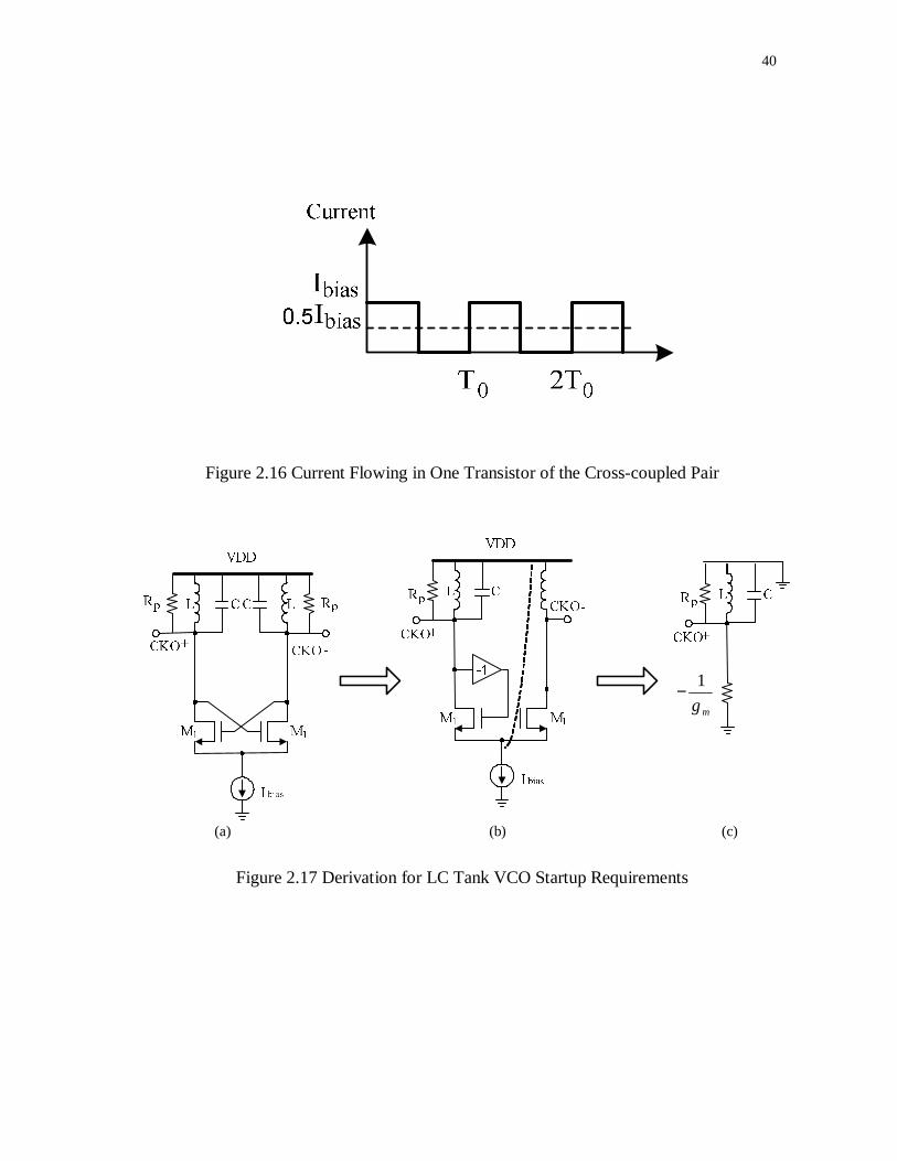
Figure 2.16 Current Flowing in One Transistor of the Cross-coupled Pair ............ 40
Figure 2.17 Derivation for LC Tank VCO Startup Requirements.......................... 40
Figure 2.18 LC Tank and Its Noise Sources Which Contribute to Phase Noise ..... 42
Figure 2.19 Properties of Cross-coupled Pair: (a) Switching Pair I-V Curve, (b) The Transconductance of the Switching Pair in Voltage Do- main, and (c) Transconductance in Time Domain [34]....................... 46
Figure 2.20 Phase Noise Measurement of a 3.3GHz LC Tank VCO..................... 49
Figure 2.21 Tuning Range of a LC Tank VCO with L=1.25nH, Ctotal=1pF ........... 51
Figure 2.22 Quadrature LC Tank VCO [35] ......................................................... 52
Figure 2.23 Diagram of Coupled Quadrature LC Tank VCO................................ 53
Figure 2.24 Explanation of QVCO Using Injection Lock Phenomenon ................ 54
Figure 2.25 Frequency Shift due to Additional Phase Shift in Coupled QVCO ..... 55
Figure 2.26 Quadrature VCO Diagram Coupled through Tail Currents................. 56
Figure 2.27 Modified Quadrature VCO Diagram Sharing Tail Currents ............... 56
Figure 2.28 Prototype IC Micrograph in 0.35µm CMOS........................................ 58
Figure 2.29 Measured Clock Spectrum of the Prototype IC.................................... 59

xiii
Page
Figure 2.30 Measured Phase Noise of the Clock Output of the CDR IC................ 60
Figure 2.31 Clock Spectrum Purity When 35MHz Sinusoidal Jitter Is Added....... 61
Figure 3.1 Optical Transceiver Block Diagram................................................... 63
Figure 3.2 Conventional PLL Based CDR Architecture...................................... 65
Figure 3.3 Proposed CDR Architecture. ............................................................. 68
Figure 3.4 Active Inductor Peaking Amplifier .................................................... 69
Figure 3.5 Half Rate Phase Detector................................................................... 72
Figure 3.6 Multiplexer with RC Source Degeneration Used to Extend Bandwidth. ........................................................................................ 74
Figure 3.7 Bandwidth Expansion of the Multiplexer Using RC Degeneration..... 75
Figure 3.8 Charge Pump and Loop Filter Configurations: ( a) Conventional Structure and (b) Proposed Configuration.......................................... 76
Figure 3.9 Charge Pump Schematic: (a) Simplified Charge Pump (CP1) and (b) The Auxiliary Charge Pump (CPA) ....................................... 83
Figure 3.10 Quadrature VCO Iimplementation ..................................................... 85
Figure 3.11 PSS Analysis of the VCO: (a) Phase Noise Simulation of the VCO, (b) Phase Mismatch between the I/Q Clocks of the VCO......... 86
Figure 3.11 Continued: (c) Phase Mismatch between the I/Q Clock of the VCO(Assume 2% Mismatch between the LC tank), and (d) VCO Tuning Curve with 6 Frequency Bands........................ 87
Figure 3.12 Varactor Model and Simulation: (a) Varactor Model and (b) Varactor Capacitance versus Input Gate Voltage ................... 89
Figure 3.13 BER Bath-tub Curve as Function of Different DJ & RJ Combinations .................................................................................... 91
Figure 3.14 Top Level Simulation Results: (a) The Eye Diagram of the Input PRBS Data with a Total Jitter (TJ) of 28.1ps, (b) The Eye Diagram of the Recovered Data by the CDR,with a TJ of 3.17ps ..................... 92
xiv
Page
Figure 3.14 Continued: (c) The Pull-in Process of the CDR Circuit ...................... 93
Figure 3.15 Chip Microphotograph ...................................................................... 94
Figure 3.16 The PCB to Test the Prototype IC...................................................... 95
Figure 3.17 Measurements Setup Diagram ........................................................... 97
Figure 3.18 Photo of a Typical Equipment Setup to Test the Prototype IC............ 98
Figure 3.19 Eye Diagram for Input Data PRBS 2^15-1 with TJ of 54.5ps............. 100
Figure 3.20 Eye Diagram of Recovered Data with Input Data Shown in Figure 3.19 .................................................................................... 100
Figure 3.21 The Recovered Half Rate Clock with 8ps Peak-to-peak with PRBS with a Pattern Length of 231-1 ................................................ 101
Figure 3.22 CDR Jitter Tolerance Measurements ................................................. 101
Figure 3.23 Jitter Transfer Measurement of the CDR Device................................ 103
Figure 3.24 Frequency Spectrum of the Recovered Clock .................................... 104
Figure 3.25 Phase Noise Plot of the Recovered Clock .......................................... 105
Figure 3.26 Measured Attenuation of 80MHz of Sinusoidal Jitter, 0.32UIpp........ 106
Figure 3.27 Measured Return Loss of the Input Buffer (< -13dB at 5GHz)........... 108
Figure 4.1 Diagram of First Order Bang-bang CDR Loop. ................................. 113
Figure 4.2 Diagram of a Typical 2nd Order Bang-bang CDR............................... 116
Figure 4.3 Slope-overload (or Slew-rate Limited) Phase Tracking Process. ....... 117
Figure 4.4 The Phase Tracking Slew Rate Limiting Process: (a) Slope Over- load Caused by Limited Bandwidth; (b) Slope Overshoot Caused by Too Small Loop Bandwidth. ......................................................... 120
Figure 4.5 The Digitized Phase Error Output of Figure 4.3: (a) Input Data Phase and (b) Phase Comparator Output. ........................................... 121

xv
Page
Figure 4.6. Delta Modulator: (a) Standard Delta Modulation Diagram (Similar to DPCM) and (b) An Implementation of DM Encoder. ....... 122
Figure 4.7 1st Order Binary CDR with Adaptive Control. ................................... 123
Figure 4.8 2nd Order Binary CDR with Adaptive Bang-bang Control.................. 123
Figure 4.9 Bang-bang Control Implementation: ( a) State Diagram of the Adaptive Bang-bang Control, (b) Adaptive Control Logic Diagram... 127
Figure 4.10 Variable Gain Amplifier Using Source Degeneration......................... 128
Figure 4.11 1st Order Markov Chain Phase-state Model........................................ 131
Figure 4.12 The Probabilities of Up, Down and Hold Signal in Proposed CDR .... 132
Figure 4.13. Comparison of the Steady State Phase Probabilities for the Transition Probabilities...................................................................... 132
Figure 4.14 The Logarithmic Plot of the Steady State Probabilities of Proposed and Classic BB CDR. ........................................................................ 133
Figure 4.16 Comparison of Phase Tracking between 1st Order Conventional and Adaptive BB CDR: (a) Phase Tracking of Conventional BB CDR, (b) Phase Tracking Error of Classical CDR, (c) Phase Tracking of Adaptive BB CDR, (d) Phase Error of 2MHZ SJ in Adaptive BB CDR and (e) Phase Tracking Error Comparison between Adaptive BB CDR and Conventional CDR....................................................... 138
Figure 4.17 Phase Comparison of x1, x3 2nd Order , BB CDR and 2nd Order Adaptive BB CDR, Frequency Difference Is 300ppm: (a) Phase Tracking of Adaptive BB CDR, (b) Phase Tracking Error of Adap- tive BB CDR, (c) Phase Tracking of Conventional BB CDR(x1 band- width), (d) Phase Tracking Error of Classical BB CDR(x1 BW), (e) Phase Tracking of Conventional BB CDR(x3 BW),(f) Phase Tracking Error of Conventional BB CDR(x3), (g) Comparison of CDR(x1BW) vs. BB CDR(x3), (h) Comparison of BBCDR(x3) vs. Adaptive BB CDR; and (i) The Comparison of CDR(x1),CDR(x3) and Adaptive CDR. ........................................................................... 141

xvi
Page
Figure 4.18 Comparison of Phase Error Tracking of Adaptive Bang-bang CDR and Classical Bang-bang CDR: (a) Adaptive Phase Error Tracking, (b) Phase Error in Adaptive Bang-bang CDR, (c) Classic Bang-bang Phase Error Tracking(Slew Rate Limiting), (d) Classic BB CDR Phase Error Tracking, and (e) Phase Error Comparison. .................... 142

xvii
LIST OF TABLES
Page
Table II.1 Alexander Phase Detector............................................................... 25
Table III.1 Design Parameters of the Multiplexer ............................................. 75
Table III.2 Design Parameters for the Filters Shown in Figure 3.8.................... 76
Table III.3 Component Values for Same Charge Pump-Filter Response ........... 80
Table III.4 Transistor Parameter for Both Charge Pumps................................. 81
Table III.5 Component Values of the QVCO in Figure 3.8(a)........................... 88
Table III.6 Summary of the Measurement Results for 215-1.............................. 110
Table IV.1 Step Size Adjustment for the Proposed CDR .................................. 126
Table IV.2 Summary of Simulation Results ..................................................... 139

1
I. INTRODUCTION
I.1. Background of Optical Communications
The volumes of data transported over the telecommunications network have
increased at a compounded annual rate of 100% from 1995 to 2002 in the US, mainly
due to the increased Internet traffic. The call for technologies, such as the interface that
expands the capacity of fiber-based transport links to10Gb/s (and beyond) has risen
recently [1]. The Synchronous Optical Network (SONET) protocol has long become the
standard in optical communications used in wide area networks (WAN). SONET
standard specifies a set of transmission speeds, all of which are multiples of “OC-1” rate,
which is 51.84 Mb/s. Currently OC-192, running at approximately 9.95328 Gb/s, will be,
or, are being deployed throughout North America, due to the rising response to the
explosion in data traffic. As a result, there is a great demand for low cost and fully
integrated transmitter (TX) and receiver (RX) chips to be deployed in the internet
backbone router, which is the core element in the network infrastructure [1].
A typical OC-192 transceiver is shown in Fig 1.1.A network processor converts
input data into the form of 16 parallel signals, each operating at 622Mb/s. These signals
are sent to the parallel inputs of the transmitter where they are synchronized to a precise
reference clock and then serialized so that the output of the transmitter is a single
channel operating at 9.95328Gb/s.
This dissertation follows the style and format of IEEE Journal of Solid-State Circuits.

2
Figure 1.1 OC-192 Transceiver Architecture
The high speed serial transmitter output is used to modulate a laser driver, which
generates the optical signal that is sent through the optical fiber. More details of the
transmitter and receiver (transceiver) are shown in Figure 1.2. At the receiving side of
the fiber, the light is applied to a photodiode connected to a trans-impedance amplifier
(TIA) which then converts the signal back to electronic form. The transmitter and
receiver (transceiver) is shown in Figure 1.2. The electronic signal is applied to a post-
amplifier and then a limiting amplifier before it is passed to the clock data recovery
(CDR), which extracts and recovers a clock synchronized to the incoming data stream at
the input of the receiver. At the receiver side, a clock synchronized to the incoming data
is generated using a clock data recovery (CDR) circuit. The recovered clock and re-
timed data provided by the CDR are then applied to a de-multiplexer (DeMux) which
outputs 16 parallel signals, each at 622Mb/s. These signals are applied to another
network processor which performs the necessary overhead and framing operations.
Among the transmitter and receiver blocks, CDR is the most critical and difficult block
to design.

3
This research is focused on the design of the clock data recovery (CDR) IC for high
speed data communications. As an example, Optical OC-192 CDR was designed to
study the circuit implementation techniques.
As an initial phase, we designed a 2.5Gb/s OC-48 transceiver using TSMC 0.35um
technology, such that some design experience was accumulated on the transceiver design.
However, due to the limited cut-off frequency of the MOS transistors in TSMC 0.35um
technology, it is not possible to design a 10Gb/s transceiver in TSMC 0.35um CMOS
technology. Hence, the OC-192 CDR was finally designed in the TSMC 0.18um
technology.
Figure 1.2 Optical Transceiver Block Diagram
The primary objective of this project is to design, layout and characterize an
integrated clock data recovery circuit operating at a clock frequency of 10 Gb/s for OC-
192 optical communications. The previously reported 10 Gb/s CDR ICs require off-chip

4
loop capacitors that increase the difficulties of system design; increasing the pin counts,
making the system more sensitive to external noise sources, and increasing the difficulty
for PCB layout. For PCB design, the loop filter capacitor has to connect to the chip, and
the routing complexity increases especially when the IC is packaged in flip-chip Ball
Grid Array (BGA) package. This research is focused on implementing a fully integrated
CDR IC and demonstrates the feasibility of the proposed design approach by using a
new configuration to efficiently generate the equivalent full on-chip solution.
Also, in the practical applications of data communications and telecommunications,
due to the variety of the noise sources, the data from the Fiber and backplane is jittery,
and the jitter frequency is in general not known in advance, thus the CDR device has to
re-time the data with an unexpected in-band jitter ranging from 50KHz to 80MHz, which
is also noted as jitter tolerance. In this research work, a CDR architecture is proposed to
track the data jitter adaptively, which is different from the conventional CDR
architecture which can only track specific small range of in-band jitter.
I.2. Jitter Requirements of the CDR Device for Optical Communications
I.2.1. Jitter Transfer Specification
For the typical applications in Telecommunications, a chain of repeaters, which
constitute both transmitter, receiver, laser driver and photo diode devices, are used to
regenerate data to long-distance, thus any jitter in one PLL can accumulate to a

5
significant level in a series of tandem PLLs [2]. The jitter transfer function of a CDR
circuit represents the relationship between output jitter versus the input jitter, which is
the same as the closed loop phase response of a PLL, i.e, the output phase response
versus the input phase across different input frequencies.In Figure 1.3(a), a chain of
repeaters are drawn to help define the jitter transfer. The data Vi transmitted at the head
of the chain has a clock data recovery based on a PLL, and the data is re-timed as V1.
After some distance of transmission, distortion and noise require that the signal to be
regenerated. For long-distance telecommunications, repeated clock data recovery
operation may occur as many as several hundred times [2]. At the end of the chain, the
output is Vo, which is the regenerated data from Vi. Each CDR circuit in the
transmission path adds its own jitter to the total jitter of the chain. The accumulation of
the jitter is described in Figure 1.3(b). Assume that the input data jitter θi is zero, and the
static phase error of each PLL is the same, and thus each PLL has the same effective
phase θs which is due to static phase error and data pattern. The jitter transfer function
(JTF) of a PLL, H(jω), is typically a low pass function between phase of the PLL output
and that of the reference clock. The response H(jω) is applied not only to the jitter
introduced in the same repeater, but also the jitter introduced in all repeaters upstream.
Then the overall transfer function from θs to the last stage output phase θo at the output
for N repeaters can be represented as:
( ) ( ) ( ) ( )( )ω
ωωωωjH
jHjHjHjH
NN
i
itotal −
−==∑= 1
1
1
(1.1)

6
For a given H(jω) and jitter power spectrum, this relation allows us to predict the
total jitter as a function of the number of repeaters. To reduce the jitter accumulation
effect in a chain of repeaters, the jitter transfer specification that is defined in the
Telecordia GR-253-CORE [3] standard requires the jitter peaking to be less than 0.1dB,
and the corner frequency (fc) is defined in Figure 1.4. For the data rate of OC-
192(10Gb/s), the corner frequency is 120KHz, which is difficult to meet even if using
LC tank VCO. However, as pointed out in [4], the jitter transfer characteristic can be
shaped by the transmitter, which typically uses a PLL with a low bandwidth of 120KHz.
Figure 1.3 Jitter Accumulation: (a) Jitter Accumulation Diagram and (b) Jitter Accumulation in a Chain of N Repeaters
iθ
sθ
oθ
(b)
Repeater
PLL
Repeater
PLL
Repeater
PLL
(a)

7
Figure 1.4 Jitter Transfer Mask of SONET OC-1 to OC-192
I.2.2. Jitter Tolerance Specification
Jitter tolerance is a measure of the capability of a regenerator to tolerate incoming
jitter without causing the bit error rate less than 10-12[3]. The measurement is done by
OC-N/STS-N Level Fc (KHz) P(dB)
1 40 0.1
3 130 0.1
12 500 0.1
48 2000 0.1
192 120 0.1

8
applying a sinusoidal jitter with peak to peak amplitude in peak-to peak Unit interval
(denoted as UIpp, for OC-192, 1UIpp is 100ps). The jitter tolerance mask defined in the
SONET standard is shown in Figure 1.5. For example, for OC-192 applications, the high
frequency(>4MHz) jitter tolerance is required to be larger than 0.15UIpp.
Figure 1.5 Jitter Tolerance Mask of SONET OC-1 to OC-192
OC-N/STS-N Level
f0
(Hz) fobj
(Hz) F1
(Hz) f2 (Hz)
f3 (kHz)
f4
(kHz) A4 (UIpp)
A3 (UIpp)
A2 (UIpp)
A1 (UIpp)
1 10 NA 30 300 2 20 NA 15 1.5 0.15
3 10 NA 30 300 6.5 65 NA 15 1.5 0.15 12 10 18.5 30 300 25 250 27.8 15 1.5 0.15
48 10 70.9 600 6000 100 1000 106.4 15 1.5 0.15
192 10 206 2000 20000 400 4000 444.6 15 1.5 0.15

9
I.2.3. Jitter Generation Specification
Jitter generation of a CDR specifies the jitter produced by the CDR circuit with no
jitter or wander applied at the input. For a typical OC-192 CDR device, the jitter
generation should be less than 0.1UIpp, or 0.01UIpp rms jitter [3].
I.3. Currently Reported CDRs
Currently, many existing 10Gb/s CDR ICs use expensive Bipolar or SiGe BiCMOS
technology [5-9].The reported works in [10-13] adopt CMOS technology, however, all
the implementations need off-chip loop filters to meet the jitter performance which is
required by the SONET standard.
Savoj and Razavi [10] proposed a reference-less CDR which uses a double edged
DFF based binary phase detector(BPD) and frequency detector(FD). The CDR
architecture is shown in Figure 1.6. As can be seen in Figure 1.6, the whole CDR
implementation is a dual-loop design which features both phase detection and frequency
detection capability. The BPD shown in Figure 1.7 was first proposed by Anderson in
his patent[14], and the frequency detector in Figure 1.8 uses two of the aforementioned
DEFF BPDs. The frequency detector uses an 8 clock phase’s clock. The architecture is
basically the CMOS implementation of the previous work of Buchwald’s GaAs HBT
realization [15]. Although the implementation does not need a reference clock, it has
limited frequency locking range when the data has long runs of 1’s or 0’s, and hence
affect the jitter tolerance performance. As reported in [10], the IC realization based on

10
this approach is not able to pass jitter tolerance mask defined in SONET OC-192
standard.
Cao [11] proposed a full rate, dual loop CDR architecture with reference clock. The
CDR uses a full rate linear phase detector whose output is proportional to the phase
difference between the data and the VCO output. The pulse width is proportional to the
phase difference, which is very difficult to control in 0.18µm CMOS technology with a
unity gain frequency ft of only 50GHz. For a robust design, the ft has to be at least ten
times of that of the data rate frequency.
Figure 1.6 Reference-less CDR Architecture in [10]

11
Figure 1.7 DEFF Phase Detector
Figure 1.8 Frequency Detector Used in [10]
VFDPD1PD2CK135 CK45CK90 CK0 VPD1VPD2 D QQDD QQD MUXData

12
Rogers and Long [12] proposed a binary phase detector CDR architecture that does
not include the frequency acquisition loop. The implementation features a LC delay cell
based ring oscillator which is depicted in Figure 1.9, and slightly passed the jitter
tolerance mask. This topology has very small pull-in range of only 0.21%.Adding a
frequency detection loop will remedy this issue. However, the LC delay cell based
oscillator is prone to process variations, which adds the difficulty in the oscillator
modeling. Moreover, the LC delay cells consume large silicon area.
Figure 1.9 Ring Oscillator Using LC Delay Cell
In 2006, Sidiropoulos [13] used a DLL based CDR architecture. Since the DLL is a
first order system, hence the resulting CDR has worse jitter tolerance and more jitter
generation than PLL based CDR when asynchronous/Mesochronous operation is enabled.
I.4 Main Contribution of This Work
A major limitation of all previously reported topologies is that all of them use off-
chip loop filters. So stringently they are not monolithic integrated designs. This research
13
work is focused on the integration of the whole CDR on a full on-chip solution, and by
adopting a new loop filter configuration. The required zero and poles are generated by
adding two feed-forward paths, and hence the use of expensive large capacitor
integration is obviated.
In telecommunication and data communication systems, the noise and hence the
jitter with the incoming data is not well known in advance, which increases the difficulty
of the CDR to regenerate the original data. The second proposed CDR architecture
utilizes an adaptive bang-bang control algorithm, which adjusts the CDR bandwidth
under slope overload situation and steady state separately. The architecture is in essence
an adaptive delta modulation (ADM) which predicts the actual CDR loop dynamics
according to the past history. Comparing with the conventional Bang-bang CDR solution,
the proposed architecture can adaptively adjust its bandwidth to tolerate the unknown
jitter existing in the system and hence improve its jitter tolerance capability.
Besides, in this research, the study of the nonlinear properties of the bang-bang
CDR is performed in detail. Due to the nonlinear nature of the phase detector used, a
bang-bang CDR can not be simply analyzed using classical control theory as that in
linear PLL/CDR system. In this dissertation work, for the first time, the describe
function analysis method is used for the evaluation of the equivalent bandwidth of a
bang-bang CDR.
This dissertation is organized as follows. Section II introduces the building blocks
for the clock recovery applications. In Section III, a full on-chip CMOS Clock Data
Recovery IC for OC-192 Applications is described in detail. A half rate binary phase

14
detector and the Quadrature VCO design contributed to the low power performance of
the test chip. A dual charge pumps configuration and the on-chip loop filter realization
lead the designed chip to a cheaper solution with higher jitter tolerance capability.
Section IV describes a multi-Gigabit/s Clock data recovery architecture using an
adaptive bang-bang control strategy. Finally the conclusions are drawn in Section V.

15
II. BUILDING BLOCKS FOR CLOCK DATA RECOVERY APPLICATIONS
Clock data recovery (CDR) is the key element of the telecommunication and data
communication applications. A typical diagram of the conventional PLL based CDR is
shown in Figure 2.1. The basic building blocks are input/output buffers, phase detector,
charge pump, passive loop filter and VCO. Among the blocks, the input buffers amplify
the input data amplitude for the phase detector to detect; the phase detector is used to
generate the phase error between the input data and the VCO output; charge pump and
loop filter are used to generate the control voltage for the VCO; the VCO is the clock
generator.
Figure 2.1 CDR Diagram
PhaseDetectorRecovered clockRecovered dataSerialdata VCOC2InputBuffer ChargePump VC1R C
16
The Phase detector (PD) architectures for clock data recovery applications mainly
include two categories: linear phase detector and binary phase detector. As shown in the
following sections, the linear phase detector outputs the phase error which is
proportional to the phase difference between the incoming data and the VCO output,
while the binary phase detector outputs only the sign of the aforementioned phase
difference. Thus the linear PD based CDR can be designed using linear analysis, while
the binary PD based CDR can only be analyzed using nonlinear design procedure, which
makes the design more complex. Secondly, when the data rate is in the range of 10Gb/s,
the output of linear PD is the fractional potion of 100ps, which is very difficult for the
prevalent CMOS technology, so quarter rate or even 1/8 rate phase detector with 4 or 8
slices of data path has to be used, which makes it very challenging to match several
branches of high speed blocks. On the contrary, the binary phase detector only needs to
output the sign of the incoming data and VCO output, so a full rate or a half rate
implementation is possible. Thus the binary PD is preferred over the linear PD in the
CDR design in recent publications of OC-192 ICs [13].
II.1. Linear Phase Detector
In the linear phase detectors that are used in the clock data recovery applications,
Hogge Phase detector is used most frequently due to its inherently smaller jitter
generation comparing with binary PD in low speed telecommunication products.

17
II.1.1. Hogge Phase Detector
A Hogge phase detector compares each data transition with the rising (or falling)
edge of the retiming clock and generates pulses whose widths are proportional to the
phase difference between the input data and clock[16]. Due to the random nature of the
input data, it is not straightforward to compare the clock and data directly to extract the
phase difference. However, by comparing with the input data and a delayed replica of
the input data [16], the phase difference between the data and clock can be extracted
indirectly. As illustrated in Figure 2.2, the random data is delayed by two D-FFs. One of
the FFs samples its input on the rising edge of the clock and the other one samples it at
the falling edge. The timing diagram is shown in Figure 2.3. Assume there is no clock-
to-Q delay for the time being, if the clock is correctly aligned to the data, since the data
at point B is a replicated version of the input data with a delay of exact half period of the
clock. At the output of XOR1, the pulse at Y is then a half period of the retimed clock. If
the input data Din has timing mismatch with the retimed clock, the pulse width will be
smaller (or larger) than half a cycle of the retiming clock if the clock is early (or late)
than the optimum. While the output at XOR2 is a constant half period of the retime clock.
The difference between the pulse Y and X gives out the phase difference between the
input data Din and the retimed clock. Also, the pulses Y and X occur for every transition
of the data. The pulse width at Y is directly proportional to the phase difference between
the input data and retime clock, sometimes it is called proportional pulse. The pulse
width at X is always half a cycle of the retime clock; it is often referred as reference.

18
Figure 2.2 Hogge Phase Detector Implementation
Figure 2.3 Timing Diagram of Hogge PD When Locked

19
One of the important features of Hogge phase detector is the automatic retiming of
the incoming sequence. In the locked condition, the zero crossings of the clock signal
appear in the middle of the data eye, which is the optimum point for data retiming.
Figure 2.4 Characteristic of Hogge Phase Detector
However,as pointed out in [17], the Hogge phase detector has the retiming delay
through DFF2, which leads to a half period skew between the pulses at XOR1 output
Y(error) and XOR2 output X(reference). It can be concluded that, even in lock condition,
a charge pump and loop filter driven by Error and reference produces a positive ramp
when the reference is high, the control voltage of the VCO then experiences a triwave
with a positive net area as in Figure 2.3. This positive net area will cause static phase
offset in the retimed clock output even in the lock condition. The resultant control
voltage versus phase difference transfer curve is illustrated in Figure 2.4, where the
horizontal axis φ is the phase difference between the input data and recovered clock. It

20
can be seen that the relationship between the control voltage and phase difference is
linear within [-π, π]. Figure 2.5 Clock-to-Q Delay Effect on the Hogge PD Output
As one remedy, Tom Lee and John Bulzacchellia modified the architecture which is
so-called triwave phase detector to remove the static phase error [17],[18].By including
two more registers, the “half period skew” limitation of the Hogge PD is solved. Though
the triwave detector exhibits a much reduced sensitivity to data transition density, it is
more sensitive to duty cycle distortion in the clock signal.
The above discussion does not consider the clock-to-Q delay of the DFFs used,
which is sown in the timing diagram of Figure 2.5. And the clock-to-Q delay causes
static phase offset when it is used in a CDR/PLL, thus it should be subtracted from the

21
pulse at Y. A potential solution to this issue is to add a delay cell to compensate for the
Clock-to-Q delay in the Hogge PD as shown in Figure 2. 6.
Figure 2.6 Delay Compensation for the Clock-to-Q Delay Effect
II.1.2. Limitations of the Hogge Phase Detector
Although the Hogge phase detector has inherently small jitter generation due to the
PD itself compared with the binary PD, it still presents some limitations.
Firstly, the Hogge Phase detector gain is sensitive to incoming data transition
density. Assume the incoming data pattern changes from “010101…” to
“001100110011….”, the phase detector gain will be reduced by half. Secondly, the
Hogge phase detector has inherently small jitter generation due to the PD itself
compared with the binary PD such as Alexander PD.

22
The Hogge PD is limited by the bandwidth requirements; as stated before, it is
difficult to design a Hogge PD for 10Gb/s applications. Most important, the mismatch
between the DFFs in the circuits will cause static phase offset, and thus affects the jitter
performance of the CDR circuit.
Due to the above limitations, Hogge phase detector is usually not adopted in 10Gb/s
CDR design.
II.2. Binary Phase Detector
Several state of the art implementations for 10Gb/s and 40Gb/s CDR adopted the
binary phase detector architecture due to the difficulty to generate the narrow pulses in
currently available CMOS/BiCMOS technologies with a ft in the range of 60GHz to
120GHz. These techniques are revisited in the following subsections. Among these
binary phase detectors, Alexander phase detector is used most frequently.
II.2.1. Alexander Phase Detector
As shown in Figure 2.7, the Alexander PD samples the input data signal at three
time instants[5-7],[19-21]. S1 and S3 sample two consecutive bits while S2 samples the
data transition, as indicated in Figure 2.7. By comparing whether the transition is close
to S1 or S3, clock early or late can be determined. If the three samples S1, S2, and S3 are
the same, there is no transition during the decision process, thus there is no decision
from the PD output. The summary of these operations are tabulated in Table II.1 for

23
clarity. Notice that, when the samples of S1,S2, and S3 are the same, or have alternate
pattern of ‘0’ and ‘1’, the PD output will not change, i.e., no decision will be made.
Figure 2.8 shows an implementation of the Alexander PD[21]. The S1, S2, and S3
samples of input data in Figure 2.7 are generated by using three D-Flip-flops (DFF) and
one latch; two Exclusive OR(EXOR) elements are used to generate the early and late
signals. As a modified version of the PD, the DFF which generates S1 can be changed to
a latch, while the latch to generate S2 is removed; the resultant overall function keeps the
same as that in Figure 2.8. The ideal characteristic transfer function is shown in Figure
2.9. The control voltage versus the phase difference transfer curve is like a step function,
just because the Alexander PD only outputs the sign of the phase difference instead of
the magnitude. However, due to the limited speed of the DFFs that are used in the PD,
the transfer curve flattens as shown in Figure 2.10 [22]. It can be seen that the PD linear
range is 2δ, which is usually less than 6π according to [22], thus the linear range is far
smaller than that of the Hogge PD shown in Figure 2.7. As will be shown in the next
sections, the Alexander PD based CDR is a nonlinear architecture, thus the conventional
linear control theory can not be directly used for its analysis, which makes its design
more difficult.

24
Figure 2.7 Binary Phase Detector: (a) Clock Is Early, (b) Clock Is On-time and (c) Clock Is Late
(a) clock early
(b) clock on-time
(c) clock late

25
TABLE II.1 ALEXANDER PHASE DETECTOR
S1 S2 S3 Operation
0 0 0 No Decision
0 0 1 Clock is fast (early)
0 1 0 No Decision
0 1 1 Clock is slow (Late)
1 0 0 Clock is slow (Late)
1 0 1 No decision
1 1 0 Clock is fast (early)
1 1 1 No Decision

26
Figure 2.8 Alexander Phase Detector
Figure 2.9 Ideal Transfer Function of Alexander PD
ϕ

27
Figure 2.10 Non-ideal Transfer Function of Alexander PD
II.2.2. Limitations of the Alexander PD
Although the Alexander PD can detect whether the clock phase is ahead or later
than the optimal sampling instant, it does not indicate the magnitude of the phase error
as the linear PD does. In general, the jitter of the Alexander PD CDR is worse than that
of linear PD CDR. However, for applications above 10Gb/s or 40Gb/s, the available
technology such as 0.18 µm BiCMOS, achieves the unity gain frequency ft up to 120GHz.
The ft is only 12 times and 4 times larger than the clock frequency of 10Gb/s and 40Gb/s
systems. Under such situation, the linear phase detector needs to generate very narrow
pulses proportional to the phase difference. On the other hand, the Alexander phase
δ− δ ϕ

28
detector only needs to detect the sign of the phase difference, thus it can achieve higher
speed than Hogge PD. Thus Alexander PD can still be a trade-off between the
performance and design challenge.
In summary, the Alexander PD is nonlinear in nature and generates higher jitter due
to its nonlinear nature. Because it detects the sign of the phase error instead of the
magnitude as linear PD does, it presents more jitter generation than a linear PD. The
Alexander PD is a binary phase detector, thus the linear analysis can not be used to
explain its behavior. However, as the Alexander PD can potentially run at higher speed
than Hogge PD does, in this research, a binary phase detector is adopted.
II.3. Phase Frequency Detector
II.3.1. Pottbaker PFD
The Phase frequency detector proposed by A. Pottbacker and U. Langmann [23] is a
digital implementation of the Quadricorrelator reported in [15]. The in-phase and
quadrature mixers are replaced by the double edge triggered DFFs as shown in Figure
2.11. However, this circuit has limited tuning range. It was reported that at nominal
frequency of 8GHz, frequencies errors on the order of 100MHz can be acquired. In this
research work, a similar architecture is used for the phase detector.

29
Figure 2.11 Block Diagram for Pottbacker PD Based CDR Implementation
II.3.4. Conclusion
In Linear phase detectors such as Hogge detector, the output pulse width is linearly
proportional to the input phase difference, resulting in a constant loop gain during lock
transient and minimal charge pump activity after phase lock is achieved. The difficulty is
how to generate the pulse widths equal to a fraction of the clock period at speeds near
the limit of the technology. While the Bang-bang PDs employ simple flips flops for
maximum speed, they provide only two output states, creating significant ripple on the
control line even in the locked condition and producing larger jitter at the VCO output.
Thus there is a trade-off when selecting the linear or binary PD. In this research work,
binary PD is adopted considering the speed requirements and technology available when
this research work is performed.

30
II.4. Charge Pump
II.4.1. Single-ended Charge Pump
Single-ended charge pumps are used extensively since they only need one loop filter
and thus consume less power in tri-state operation. In the standard frequency synthesizer,
the output current of the charge pump can be as high as several mA [24] to provide
better spur performance over the leakage current and to have high SNR at the charge
pump for low noise contribution to the PLL. A typical configuration is shown in Figure
2.12 with switches at the drain of the transistors in the current mirror [24],[25].
II.4.1.1. Single-ended Charge Pump with Switches at the Drain of Current Mirrors
Figure 2.12 shows the charge pump with the switch at the drain of the MOS
transistors in the current mirror. When the switch DN is turned off, the drain of M1 is
pulled to ground. After the switch DN is turned on, the voltage at the drain of M1
increases from 0V to the voltage held by the loop filter. For proper operation, M1 has to
be in the linear region till the voltage at the drain of M1 is higher than the minimum
saturation voltage, Vdsat.
During the transient time the drain current of M1 and the switch Msw are described by
equations (2.1) through (2.3).

31
( )( ) ( ) −−−−−= 21,,,, 2
1,
11 MdctlMdctlMthMdDDM
oxnMD VVVVVVVL
WCuI
sw
SW
sw (2.1)
( )( ) −−= 21,,,
11, 2
1,
111 MdMdMthMgM
oxnMD VVVVL
WCuI (2.2)
1,, MDMswDD III −=∆ (2.3)
where VDD is the power supply voltage, Vg,M1,Vd,M1 and Vth,M1 are gate voltage, drain
voltage and threshold voltage of M1; Vth,Msw is the threshold voltage of the switch
transistor Msw; Vctl is the control voltage at the charge pump output. From (2.1-2.13),
even if the W/L sizes of M1 and Msw are the same, the currents of the two transistors
change with the variations of the drain voltage of the M1 and the threshold changes of
Msw when the switch is turned on, until the M1 is in saturation. Thus high peak
current(spike) is generated. In other words, if solving the equation 0=∆ DI , the solution
of the root does not necessarily always exist with the variation of Vd,M1. And the
matching of the peak current in NMOS current mirror with that in PMOS mirror is
difficult since the amount of the peak current varies with the charge pump output voltage
[24]. When the switch at the drain of M1 is turned off, there is charge injection into the
output node of the charge pump, and the generated current spike also affects the
performance of the charge pump.
Because of the limitation of generating high peak current when the switches is on
from off or vice versa, other charge pump configurations have to be considered. In the
following sections, more charge pumps will be discussed.

32
Figure 2.12 Single-ended Charge Pump: Switch at the Drain
II.4.2. Improved Charge Pump
In addition to the typical single-ended configuration discussed previously, some
variations of the charge pumps can be adopted to improve the performance.
II.4.2.1. Charge Pump with Active Amplifier
To reduce the high peak current issue in Figure 2.12, one potential solution is by
replicating the UP and DN switches with its gate controlled by the inversion signals of
UP and DN, i.e., UPand DN ,respectively, thus the current source (M1 or M2 in Figure
2.12) is always on. The differential charge pump with an active amplifier [26-27] is
shown in Figure 2.13(a), where the current sources Idn and Iup are equivalent to M1 and

33
M2 in Figure 2.12, respectively. With the unity gain amplifier, the voltage at the drain of
M1(Idn) or M2(Iup) is set to the voltage at the output node when the switches are off. By
doing this way, the voltage difference between the charge pump output and the drain of
M1 (or M2) is reduced, and less peak current is generated comparing with the single-
ended charge pump in Figure 2.12.
II.4.2.2. Charge Pump with Current Steering
The charge pump with the current steering switch is shown in Figure 2.13(b). The
performance is similar to the one shown in Figure 2.13(a), but the switching time is
reduced by using the current switch [24], where the turn-on time of the switch is smaller
than the slewing of an amplifier which has smaller bandwidth to reduce power in Figure
2.13(a). This architecture can be easily converted into differential version as done in [18],
[24].
II.4.2.3. Charge Pump with NMOS Switches Only
In Figure 2.13(c), the inherent mismatch of PMOS transistor and NMOS transistor
is avoided by using NMOS switches only [19],[24],[28],[29].However, the pole which is
caused by the diode connected transistor M6 limits the speed of the charge pump. If large
current is used, the transconductance of the M6 is increased, thus the limitation of M6
can be greatly alleviated. In order to counteract this effect, a differential implementation
34
as [11] can be adopted in spite of the area increase of the differential loop filter.
II.4.3. Summary
In this work, the charge pump with active amplifier in Figure 2.13(a) is used for its
better performance comparing with that in Figure 2.12.However, even though the peak
current issue in Figure 2.12 is solved by using Figure 2.13(a), there is charge sharing
issue when the UP or DN switch is turned on from the off state, or vice versa. These
charge sharing can be easily reduced by adding dummy transistors operating in the
complementary phases of the switches. For 2.13(c), a differential implementation will be
further addressed in Section III.
II.5. Voltage Controlled Oscillators
Voltage controlled oscillator (VCO) is one of the most important blocks in high
speed CDR design. To meet the jitter or phase noise specification of the CDR, the VCO
has to meet the following criteria: Good spectral purity or low phase noise Reasonable power consumption Large tuning range

35
Figure 2.13 Improved Single-ended Charge Pump Architecture: (a) With Active Amplifier, (b) With Current Steering and (c) With NMOS Switches Only Relatively small sensitivity (VCO gain)

36
In recent designs, ring oscillator and LC tank oscillator are the most frequently used
architectures in frequency synthesizer and CDR applications. Optical communication
applications require using low phase noise VCO. Thus, in this research, only LC tank
oscillator is adopted due to its lower phase noise performance compared to ring
oscillators [30].
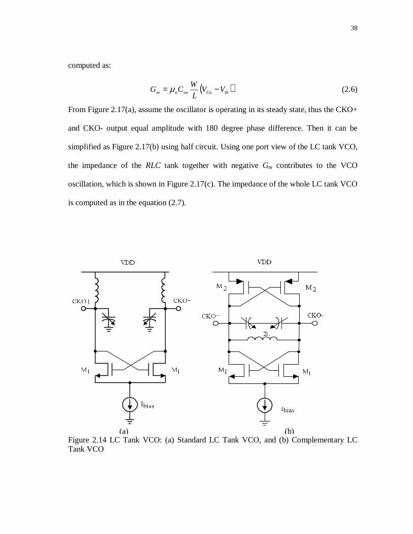
II.5.1. LC Tank VCO
II.5.1.1. Startup Behavior
LC tank VCO is used in wireless transceivers because of its low phase noise
performance. According to the topology, the LC tank oscillator can be divided further
into single cross-coupled pair and complementary cross-coupled pair topologies
[21],[31], which are shown in Figure 2.14(a) and Figure 2.14(b).
In Figure 2.14(a), the cross-coupled differential pair constitutes a small signal negative
differential resistance -2/gm across the LC tank to compensate for the series loss
resistance of the inductors. When the bias current is large enough to start the oscillation,
the oscillation amplitude is larger than the voltage required to switch the differential
pair, i.e. ( )thgs VV −2 , then the cross-coupled pair transistors conduct currents to the LC
tank to sustain the oscillation by compensating for the loss of the tank.
Figure 2.15 shows the currents in the cross-coupled differential pair and the VCO
output. It can be seen that the currents in the differential pair are close to square

37
waveform.
As depicted in Figure 2.16, once the VCO starts oscillation, the currents flowing in
the cross-coupled MOS transistor pair can be described as two square waves with
amplitude of Ibias and 0, alternating in a frequency of f0, which is the VCO oscillation
frequency.
For simplicity, a square wave f(t) with a frequency of f0 ,and the amplitude of I0, the
Fouries representation as follows:
[ ] ( )∑∞=
=...5,3,1
00 sin
14
n
tnn
Itf ω
π; 00 2 fπω = ; (2.4)
Thus the VCO amplitude can be written as
pbiasAmplitude RIVCOπ2= ; (2.5)
where Rp is the equivalent parallel resistance of the inductor, sp RLR 20ω= , where Rs is
the series resistance of the inductor.
In a limited range of increasing the Ibias current, the VCO amplitude is also
increased, which is denoted as current limited region, however, when the bias current is
further increased, the amplitude reaches a single-ended amplitude of VDD, the negative
peaks momentarily force the tail current source transistor into triode region, thus the
ouput amplitude is limited, which is denoted as voltage limited region [32],[33].
The startup behavior can be analyzed from Figure 2.17. In order to cancel the effect
of the equivalent parallel resistor of the inductor, Rp, GmRp must be greater than 1. Gm is
the large signal transconductance if the tail current transistor works in saturation region,
38
computed as:
( )thGsoxnm VVL
WCG −= µ (2.6)
From Figure 2.17(a), assume the oscillator is operating in its steady state, thus the CKO+
and CKO- output equal amplitude with 180 degree phase difference. Then it can be
simplified as Figure 2.17(b) using half circuit. Using one port view of the LC tank VCO,
the impedance of the RLC tank together with negative Gm contributes to the VCO
oscillation, which is shown in Figure 2.17(c). The impedance of the whole LC tank VCO
is computed as in the equation (2.7).
Figure 2.14 LC Tank VCO: (a) Standard LC Tank VCO, and (b) Complementary LC Tank VCO
(a) (b)

39
( )( ) 1)()(
121 +−+
=+−+
= − LGGsLCs
sL
sLGGsCsZ
mpmp
(2.7)
If Gp<Gm, then we have two poles at the right plane of the Laplace S plane. Once
perturbed by the power supply or other means, the VCO oscillates and continues to build
up. Once the amplitude is large enough, the oscillator operates in a nonlinear
mechanism. If Gp=Gm, which means GmRp=1, then the two poles lie on the imaginary
axes of the S-plane, such that a stable oscillation is sustained. In real applications, GmRp
>2 is designed to help startup the oscillation stably [21].
Figure 2.15 Transient Simulation of a Typical LC Tank VCO. Note: From the Top to the Bottom, the Signals Are: VCO Differential Outputs, Currents in the Cross Coupled Transistors and Tail Voltage
40
Figure 2.16 Current Flowing in One Transistor of the Cross-coupled Pair
Figure 2.17 Derivation for LC Tank VCO Startup Requirements
VDDM1 M1+ CKO-CKO I bias
L C LCRp Rp VDDM1 M1+ CKO-CKO I biasL CRp -1 +CKO L CRp
mg
1−
(a) (b) (c)

41
II.5.1.2. Phase Noise Consideration
The oscillator output with small random excess phase can be represented as [28]:
( ) [ ])(cos 0 ttAtx nφω +=
where ( )tnφ is the excess phase.
By manipulating trigonometric operation, and notice that the excess phase is very
small, by approximating ( )( ) ( )( ) ( )ttt nn φφφ ≈≈ sin,1cos n , the x(t) can be expanded as
follows:
( ) ( ) ( )( ) ( ) ( )( )[ ]( ) ( ) ( )[ ]tttA
ttttAtx
n
nn
φωωφωφω
00
00
sincos
sinsincoscos
−=−=
(2.8)
Represented in frequency domain, we have:
( ) ( )[ ] ( ) ( )[ ] ( ) ( ) ( )[ ] ( ) ( )[ ] 0000
0000)(
ωωφωωφωωδωωδπωφωωδωωδωωδωωδπω
++−−−+−=⊗−+−−−+−=
nn
n
A
AX (2.9)
which means that the excess phase is translated into frequency components centered
around ω0.
In general, denote carrier frequency as f0, the spectral purity of an oscillator is
generally measured by using phase noise which is defined as:
( )powercarrier
ftorespectwithfoffsetanatHzwithinpowernoisef 01
=l (2.10)

42
(a) LC tank diagram (b) Noise representation of LC tank
Figure 2.18 LC Tank and Its Noise Sources Which Contribute to Phase Noise
Now from the definition of phase noise, the analysis of LC VCO will be performed
in the following paragraphs.
From Figure 2.18(a), the input impedance at ω0+∆ω, ω0 is the resonant frequency
with the value of LC1 .In Figure 2.18(b), the noise sources in the LC tank VCO
include, 2,tailni ,which is attributed to the tail current source; 2
,gmni , which is due to the
differential pair, and 2 tan, kni is attributed to the resistive element in the inductor.
( )
( )
( )LCLCLC
Lj
LC
Lj
LjCj
Z
20
20
0
20
0
21
)(1
||1
0
0
ωωωωωω
ωωωω
ωω
ωωωω
ωωω
∆−∆−−∆+
=
∆+−∆+
=
=∆+=
∆+=
(2.11)
At low frequency offset,
( )
ωω
ωω
ω
ωωωωωω
∆−=
∆−=
∆−∆+
≅∆+
Q
j
C
j
LC
LjZ
22
2)(
00
0
0
00
(2.12)
L CinZ
2tan, kni
2,gmni
2,tailni

43
where Q is the quality factor of the LC tank, which is defined as in [18]. For a parallel
RLC tank,
RCL
R
Z
RQ
CL
00,
ωω
=== (2.13)
The thermally induced phase noise density [18] due to resonator loss (mainly the
equivalent parallel resistance Rp of the inductor L in Figure 2.18(a) is:
( ) ( )
2
02
2
0
2
8
2/
4 ∆=
∆+=∆
ωω
ωωω
QA
KTR
A
ZKTR
p
pl (2.14)
where A and Q are the VCO output amplitude and quality factor, respectively. It can be
easily concluded to increase the inductor quality of factor, and to increase the VCO
amplitude, as well as reduce Rp can improve the phase noise performance.
The switching of the differential pair(cross-coupled negative Gm pair) samples the
noise in the tail currents as a single-balanced mixer [34]. The noise is frequency
modulated into the LC tank, mainly at the zero crossing point of the VCO output. Noise
originating in the tail current at a frequency of 2ω0±∆ω is down-converted to ω0±∆ω.Notice that the conversion gain of a mixer is typically π2 , the noise at the VCO
output due to the tail current source thus is:
( )2
,,
2,
24 ×= ωπ
ZGg
KTnV diffm
tailmtailn (2.15)
where n represents accumulated noise after aliasing, consider the cross-coupled pair as
mixers, then ( ) 4...513112 222 π=+++=n ; where the first term is the thermal noise

44
mixed by the fundamental tone at ω0; the second term is the noise around 3ω0, which is
downconverted by the third harmonic of the VCO, and the conversion gain is reduced to
1/3 of the main harmonic, etc.
The phase noise caused by the thermal noise at 2ω0 is reported in [32], rewrite here:
( )2
02
22,
2,
2
22
44
4 ∆×=∆
ωω
πγπω
QA
RG
g
KT pdiffm
tailm
l (2.16)
where gm,tail is the transconductance of each transistor in the cross coupled differential
pair, and γ is the noise factor in a single FET, normally it is 2/3 in long channel CMOS
technology, and larger than 1 in short channel transistors. If the Vdsat of the differential
pair and the tail current source are designed similar, using the fact of
dsat
D
Tgs
Dm V
I
VV
IG
22 =−
= , and notice the current in the differential pair is half the tail
current at the zero-corssing point of the VCO output, (2.15) can be simplified to
( ) ∆= ∆
=∆ω
ωγω
ωγωQV
I
A
RKT
QA
RGKT
dsat
tailppdiffm
2
4
224 0
2
22
02
2,l
(2.17)
For the cross-coupled differential pair, the switching of the differential pair requires
the amplitude of the VCO is larger than( )tgs VV −2 , which is the voltage required to
switch the differential pair. The differential pair sustains the oscillation by injecting an
energy-replenishing square wave into the LC resonator [33]. As depicted in [32] and
redrawn in Figure 2.19, the noise in the differential pair is actually not sampled by
impulses, but by time window of finite width. The window height is proportional to

45
transconductance, and the width is set by the tail current, and the slope of the oscillation
waveform at zero crossing. The input referred noise spectral density of the differential
pair is inversely proportional to transconductance. Thus the narrower the sampling
window, the lower the noise spectral density. Using the fact that the transconductance of
the differential pair is VIGm ∆= 2 , as shown in Figure 2.19. For sinusoidal signal with
amplitude of A, the slew rate SR is 02 ωASR= .Denote the pulse in Figure 2.19(c) as
p(t). The noise current of the cross-coupled differential pair is given in [34]:
( )A
IkT
TSR
KTIV
TSR
I
TVdttp
Ti tailtail
nw
tailn
T
diffn πγγ
441222
0
2
2
0
22
00
2, =
⋅==⋅= ∫ (2.18)
where T0 is the period of the sinusoidal VCO output, and A is the amplitude.
The phase nose due to the differential pair (with a factor of 2 due to the two
transistors in the pair) is [32]:
( )2
02 22
42 ∆=∆
ωωγ
πω
QA
RKT
A
RI pptaill (2.19)
Connecting to the famous Leeson’s model, which describes the phase noise using
the following formula [18], [23]:
( ) ∆⋅=
∆⋅=∆
2
02
2
0
2
4log10
2
2log10
ωω
ωωω
QA
FKTR
QP
FKT
p
sig
l; (2.20)
where F is an unspecified noise factor; K is Boltzmann’s constant which
is eV51062.8 −× , and T is the temperature, Psig is the power of the carrier at the
fundamental frequency of ω0, and Q is the quality factor of the LC tank, while the ∆ω is

46
the offset frequency from the carrier frequency ω0.The phase noise denotes the “decibels
below the carrier per Hz or dBc/Hz”. Due to the facto of equal split the noise into AM
and PM noise, from [34], the noise factor due to the thermal noise can be represented as:
pdsat
tailtailp RV
I
A
IRF
2
121 γ
πγ
++= (2.21)
Figure 2.19 Properties of Cross-coupled Pair: (a) Switching Pair I-V Curve, (b) The Transconductance of the Switching Pair in Voltage Domain, and (c) Transconductance in Time Domain [34]
As described in [16], when the LC tank oscillator works in a current limited region,
which means that increasing tail current, the oscillation amplitude also increases, thus
TGS VVV −=∆
TGS VVV −=∆
SR
VTw
∆=

47
second term in (2.27) is constant, namely 2γ. However, when the tail current is increased
beyond some point, the oscillation amplitude is limited by the supply, which is called
“voltage limited mode”. Thus increasing further the tail current will worsen the phase
noise because the differential pair caused phase noise takes more effect.
Assume the VCO works in current limited region, thus the noise factor can be
written as:
pdsat
tail RV
IF
2
121 γ
πγ ++= (2.22)
For a LC tank oscillator in Figure 2.14(a), with a initial guess of inductor L=1.1nH,
and quality of factor Q=7, and the resonant frequency is 5GHz, the equivalent parallel
resistance Rp is
242101.110527 990 =×××××== −πω LQRp (2.23)
The minimum tail current is
mAR
I
p
tail 24
6.0 =≥
π
(2.24)
As calculated in the Section III, the phase noise of the LC tank VCO should be less
than -100dBc at 1MHz offset to meet the jitter requirements in optical communications.
( ) 1002
4log10
2
02
−< ∆⋅=∆
ωωωQA
FKTRpl (2.25)
where mVVdsat 63> if I tail > 4mA.
Then long channel length transistor with reasonable width tail current source should
be used. Further phase noise simulation needs to be done to ensure the VCO meets the

48
noise requirements.
For completeness, there is also -30dB/decade region which is possibly attributed to
the flicker noise(1/f noise), and Leeson gave out the modified version of phase noise
equations, which is defined as [16], [23].
( ) ∆
∆+ ∆
+⋅=∆ω
ωω
ωω31
2
0 12
12
log10f
sig QP
KTl (2.26)
A typical LC tank oscillator working at 3.3GHz is shown in Figure 2.20. The phase
noise finally flattens out for large frequency offsets, rather than continuing to drop at -
20dB/decade as predicted in (2.19). That is due to the noise floor associated with any
active elements (buffers) placed between the test fixture and test equipment, and the
noise flloor limited by the measurement instrument itself.

49
Figure 2.20 Phase Noise Measurement of a 3.3GHz LC Tank VCO
II.5.1.3. Tuning Range
For a LC tank VCO in Figure 2.14(a), the total capacitance is composed of fixed
capacitance, Cfix, and varacotr, Cvar. Thus the minimum frequency is
( )maxvar,
min2
1
CCLf
fix +=
π (2.27)
( )minvar,
max2
1
mfix CCLf
+=
π (2.28)
The frequency tuning range is calculated as (fmax-fmin)/((fmax+fmin)*0.5).
20dB/decade region
30dB/decade region
Noise floor

50
For the varactor used in this research work, the Cvar,max/Cvar,min=1.8, the percentage
of the frequency tuning is shown in Figure 2.21. The maximum tuning range is 21%
when the fixed capacitance is 20% of the total capacitor tank; and 7% when the fixed
capacitance takes 70% of the overall capacitance. So it is necessary to reduce the fixed
capacitance over the varactor bank in order to achieve higher tuning range.
II.5.1.4. Summary
The LC tank VCO includes integrated inductor and varactor, thus it occupies larger
area than a LC-less ring oscillator. However, due to the higher Q of the LC tank, the
phase noise of a LC VCO(<-100dBc at 1MHz offset) is less than that of a ring oscillator,
which presents a phase noise of <-90dBc at 1MHz offset.
The LC tank VCO has limited tuning range due to the relatively low ratio of the
maximum and minimum capacitance that the varactor can achieve. Thus multiple banks
of Capacitors have to be used to increase the tuning range.

51
Figure 2.21 Tuning Range of a LC Tank VCO with L=1.25nH, Ctotal=1pF
II.5.2. Quadrature LC VCO
Quadrature VCOs, which generate I/Q phase clocks, are widely used in the RF
front- end transceivers. Also, it finds extensive usage in SerDes(Serializer and De-
serializer) devices which require half rate phase detection, phase interpolation and
frequency detection. The methods for generating quadrature phase clocks include the
following three ways:Divide-by-2 circuit, poly phase filter, and Quadrature phase
VCO(QVCO). QVCO is not always the best solution for wireless applications, for
example, a direct conversion receiver often uses divide-by-2 to avoid pulling problems.
QVCO requires more on-chip inductors and often result in larger die
0.2 0.25 0.3 0.35 0.4 0.45 0.5 0.55 0.6 0.65 0.70.06
0.08
0.1
0.12
0.14
0.16
0.18
0.2
0.22
totalfix CC
Tuning ra
nge

52
area.Moreover,QVCO is more prone to substrate coupling with more on-chip inductors.
Nevertheless, QVCO is widely used in SerDes and CDR designs. The main reason is
that, it is quite challenging to design full rate architecture if the design works at 10GHz
or above under current popular CMOS technology; the half rate architecture which uses
I/Q clocks leverage the device speed requirements.
A typical QVCO schematic is shown in Figure 2.22. Besides the LC tanks, the
transistors M1 and M2 constitute the negative Gm and the coupling transconductance Gmc,
respectively. With an equivalent circuit diagram in Figure 2.23, the coupling mechanism
can be easily explained. The two LC tanks are coupled using GmcI and GmcQ, which is
very similar to a two stages ring oscillator.
Figure 2.22 Quadrature LC Tank VCO [35]

53
Figure 2.23 Diagram of Coupled Quadrature LC Tank VCO
Denote the coupling transconductance in Figure 2.23 as Gmc, Z(jω) is the impedance
of the RLC tank, we have:
( ) ( ) ( )ωωω jCKQjZGjCKI mcQ ∗∗−= (2.29)
( ) ( ) ( )ωωω jCKIjZGjCKQ mcQ ∗∗−= (2.30)
Note that in Figure 2.23, GmcQ has a inversion sign comparing with GmcI. It can be
concluded that ( ) ( ) 022 =+ ωω jCKQjCKI , which is equivalent to .jCKQCKI ±= Then
CKI and CKQ have phase difference of ±90°, however, the phase lead or lag relationship
between them are ambiguous[35],[36], which means that two oscillation frequencies are
possible if reflecting the phase relationship into the frequency response as will be
discussed next.
+ +

54
Figure 2.24 Explanation of QVCO Using Injection Lock Phenomenon
Basically, the coupled QVCO operates away from the resonant frequency and hence
achieves worse phase noise than a stand-alone LC tank VCO, also it presents two stable
modes of oscillation with different frequencies. By explanation using injection locking
[21], as demonstrated in Figure 2.24, the injection locking shifts the frequency from
resonance so that each tank produces a phase shift of [21] = −
osc
inj
I
I1
0 tanφ (2.31)
where I inj/Iosc is also called coupling factor, and I inj denotes the current injected by one
oscillator into the other and Iosc is the current produced b the core of each oscillator.
The required frequency shift is shown in Figure 2.25.
0φ

55
Figure 2.25 Frequency Shift due to Additional Phase Shift in Coupled QVCO
As a variant of the architecture in Figure 2.22, the QVCO in Figure 2.26 share the
tail current sources for the coupling branch and oscillation LC tank respectively, i.e., the
tail nodes of the two LC tanks are shorted together, while the tail nodes of the coupling
pairs are shorted together [37]. The theory behind this is that, when one LC tank needs
less current, say the tank with output of CKI, then the bias current can supply to the tank
whose output is CKQ to sustain enough oscillation [33],[37]. In this research work, the
configuration in Figure 2.27 is used to share the coupling transistors bias current with the
LC tank, so as to supply extra current when the coupling transistors need larger bias
currents [38].

56
Figure 2.26 Quadrature VCO Diagram Coupled through Tail Currents
Figure 2.27 Modified Quadrature VCO Diagram Sharing Tail Currents
(tail nodes of each LC tank and coupling pair are shorted together)
(Tail nodes of each tank are shorted in dashed line together, coupling transistors tail node are shorted in dashed lines too)

57
In summary, Quadrature VCO inherently generates quadrature clock phases, and
with comparable phase noise performance as LC tank VCO, with more power
consumption. However, the circuits connected to the quadrature VCO can be designed in
half rate, which reduces the design complexity as well.
II.6. Experimental Results of a Prototype IC
With the system level function which is described in Appendix A, A linear phase
detector based CDR prototype IC is designed in TSMC 0.35µm CMOS technology. The
CDR Chip microphotograph is shown in Figure 2.28, which occupies an area of less than
2.5x2.5mm2. The CDR mainly uses a Hogge Phase detector shown in Figure 2.2, a LC
tank VCO as that in Figure 2.14(a), a charge pump as in Figure 2.13(a) and off-chip RC
loop filter, which is the same as that in Figure 2.1.
The output spectrum of the clock is shown in Figure 2.29. The phase noise of the
clock output is shown in Figure 2.30, when the CDR is locked to the 200MHz reference
clock; at 1MHz offset, the phase noise is -107dBc/Hz. Figure 2.31 shows that the clock
spectrum purity, with a 35MHz sinusoidal jitter modulation at the data input, the clock
output has an 27.8dB attenuation of the harmonic tone at 35MHz offset to the
fundamental tone.

58
Figure 2.28 Prototype IC Micrograph in 0.35µm CMOS
However, when the input goes to 10Gb/s, the expected clock output phase noise will
be -107dBc+9.5dB =-97.5dBc, which is marginal in implementing a 10Gb/s CDR.
Also,the speed requirements of other blocks such as phase detector and frequency
divider, necessitate a faster technology such as 0.18um CMOS to be used. In the next
section, an implementation of 10Gb/s CDR will be addressed in more detail.
Two Loop
CDR

59
Figure 2.29 Measured Clock Spectrum of the Prototype IC
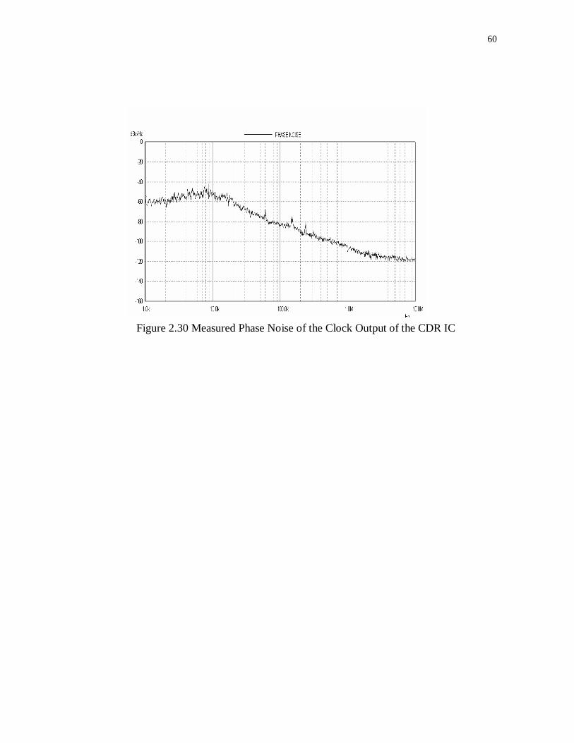
60
Figure 2.30 Measured Phase Noise of the Clock Output of the CDR IC

61
Figure 2.31 Clock Spectrum Purity When 35MHz Sinusoidal Jitter Is Added

62
III. A FULL ON-CHIP CMOS CLOCK DATA RECOVERY IC FOR OC-192
APPLICATIONS
III.1. Introduction
Demand for low cost transceiver IC has increased due to the convergence of
Datacom and Telecom network applications [5]. A typical transceiver design includes
both a transmitter and a receiver as shown in Figure 3.1. The transmitter (TX) includes a
PLL and multiplexer (MUX), which serializes the 16 bits parallel data if SFI4 interface
is used in the typical OC-192 applications. The synchronization clock is provided by a
narrow bandwidth PLL. After serialization(or MUX), the data is sent to the photodiode
through a laser driver(LD) as the interface of the single-mode Fiber or multi-mode Fiber
for long distance data transmission. At the receiver side, the transimpedance amplifier
(TIA) detects the photodiode current and converts it to voltage, and then the limiting
amplifier (LA) amplifies and limits the voltage signal to a fixed level in order to increase
the sensitivity of the clock data recovery (CDR) block. Finally, the recovered data is de-
serialized into parallel data outputs for further framing or overhead processing1.
Several 10 Gb/s transceiver ICs have been recently reported [5]-[13], many of them
are fabricated in SiGe BiCMOS [5]-[8]. More recently, efforts have been reported to
integrate the 10Gb/s CDR in CMOS technology for cost reduction and higher integration
purposes [10]-[13]. However, these designs need a large off-chip integration capacitor to
1 Overhead processing includes add-drop multiplexer.

63
meet the jitter peaking and jitter tolerance defined in the Telecordia OC-192 standard.The
off-chip capacitor increases the number of external components and pin count; also it
couples noise from off-chip to the control voltage of the VCO in the CDR block.
Another issue is that the bondwire inductor increases drastically the high-frequency
impedance of the loop filter making the CDR more sensitive to HF noise.
Gm Cell
MUX
PLL
SFI-5SFI-4XAUI
LaserDriver
ControlLogic
10Gb/s
50kmSMF
TIA LA CDR DEMUX
SFI-5SFI-4XAUI
TransmitterReceiver
Figure 3.1 Optical Transceiver Block Diagram
As shown in [39], decreased area of on-chip capacitance can be realized by using
active loop filters together with feedforward charge pumps. However, active loop filters
increase the design complexity and jitter due to noise (mainly flicker) and offset
contributions of active devices.
In [40], a sample-reset loop filter is proposed to create the stabilization zero.
Theproportional path needs a narrow pulse to perform the reset function, but the narrow
pulse generation is quite difficult in 10Gb/s CDR circuitry.

64
In this section, a fully integrated CDR architecture that obviates the need of the
large off-chip integration capacitor by adding two feed-forward paths to generate the
stabilization zero is proposed. The required capacitor in this architecture is of the order
of hundred picofarads (pFs), which is far smaller than that required by conventional loop
filter configurations. Besides, resistive source degeneration techniques used in the
auxiliary path reduce the effective input capacitance and alleviate the loading of the
phase detector. RC source degeneration techniques are adopted for zero peaking and
hence bandwidth extension in double edge D-Flip-flops (DEFF) of the phase detector
(PD) designs is obtained. The CDR can recover the PRBS data with pattern length of
215-1 and more than 0.5 unit interval peak to peak (UIpp) total jitter (54.5ps eye closure
by passing data through 9 inches FR4 PCB trace) and the total jitter of the recovered
data is 22.7ps with a RMS jitter of 0.74ps.2
The high frequency jitter tolerance of this design is over 0.31UIpp by applying a
PRBS data with a pattern length of 231-1. The CDR was fabricated in a standard 0.18µm
CMOS technology. In III 2 existing solutions and the proposed architecture are
compared. In III.3, the building blocks are described in detail. The measurements results
are discussed in III.4, and the conclusions are given in III.5.
2 Only PRBS 215-1 data pattern is applied to test the CDR recovery capability to the ISI effect. For PRBS 231-1 data, the eye closure is much heavier than 0.55UI and BER is difficult to be maintained as low as 10-
12 unless an extra limiting amplifier is inserted between the FR4 PCB trace and the data input on- chip.

65
Figure 3.2 Conventional PLL Based CDR Architecture
III.2. Description of the Architecture
III.2.1. Existing CDR Architectures
In most OC-192 CDR ICs reported, PLL based CDR architecture is preferred over
DLL based architecture because DLL is usually a first order system hence DLL based

66
CDR has worse jitter tolerance and more jitter generation. When designing multiple
channel receivers, it is advantageous to use the DLL [41], but this is not the scope of this
dissertation. The CDR architecture can be divided into linear and binary depending on
the selection of the phase detector [21]. The conventional linear and binary CDRs use a
Hogge Phase detector and Alexander phase detector, respectively. Typically, binary
CDR is widely adopted in OC-192 receiver implementation for the following reasons: i)
the D-flip-flop (DFF) in binary phase detector has inherently good match with the
retiming DFF; ii) most linear phase detectors generate narrow pulses with widths
proportional to the phase error between the timing alignment of the data and clock
signals [6]. In a typical 0.18µm CMOS technology, the narrow pulses are difficult to
generate and prone to process variations.
The diagram of a typical linear CDR is shown in Figure 3.2 [11]. The CDR includes
two loops, a frequency acquisition loop (FAL) and a phase detection loop (PDL). The
VCO’s frequency is tuned through two control mechanisms: proportional control which
directly modulates the VCO control port by the phase detector (PD) output directly and
integration control which slowly tracks (integrates) the variations at the output of phase
detector through an integration capacitor. The proportional and integration controls have
basically the same effect as using a charge pump together with a filter made of a series
resistor and a capacitor [8]-[9].Although this architecture is used frequently in the past,
the dual loop linear CDR limits its performance due to two drawbacks. Firstly, the linear
phase detector can not run at very high speed under current CMOS technology. Secondly,
the CDR needs a large off-chip capacitor which is difficult to integrate on-chip. The

67
extra pin for the off-chip cap can potentially cause noise which affects the jitter
performance of the CDR design.
III.2.2. Proposed CDR Architecture
The previously reported architectures need an off-chip loop filter or integration
capacitor to meet the jitter specifications. The proposed CDR employs the conventional
dual-loop architecture but the multiplexer is inserted before the charge pump CP1 and an
auxiliary charge pump CPA is connected to the loop filter as shown in Figure 3.3. A
similar technique has been reported in a patent which was recently released [42].
The frequency acquisition loop uses a conventional linear phase frequency detector,
while the phase detection loop adopts a half rate, double-edge DFF (DEFF) based binary
phase detector which is similar to that reported in [10]. Although the DEFF phase
detector may allow to eliminate the frequency acquisition loop, the FAL was included to
ensure enough frequency locking range. The switching between the FAL and PAL loops
is controlled by a lock detector which works at the reference frequency of the FAL.
Upon power-up, a successive-approximation register (SAR) type controller performs a
coarse tuning for the VCO to within 1% frequency error of the target frequency by
switching in or out a MIM capacitor bank and tuning a large coarse tuning varactor.
Once the frequency difference between the internally divided clock and the reference
clock is within 300ppm, the CDR will switch to the phase detection loop.

68
Figure 3.3 Proposed CDR Architecture
The phase detection loop uses a couple of charge pumps (CP1 and CPA ). CP1 and
loop filter enables the operation of a regular charge pump; the location of the zero-pole
pair is determined by the time constants R(C1+C2) and RC2, respectively. In absence of
the CPA, the spacing between the pole and zero frequency is entirely determined by the
capacitive spread between C1 and C2. Low frequency noise signals injected into the
loop filter are integrated by C1+C2 while high frequency signals are absorbed by C2

69
only. Therefore, it is desirable to increase as much as possible C2 to make the loop filter
more robust against medium and high frequency noise current injected at node Vc in
Figure 3.3. Since C1 is often more than 15*C2 to ensure enough loop phase margin,
often C1 values are in the range of nF, making very difficult to have full on-chip
solutions.By adding the CPA more flexibility is introduced for the design of the loop
filter and allows us to increase C2 for a given zero-pole location. As demonstrated in
section III.C, another benefit is that the zero-pole location is still determined by C1/C2
but also by the ratio of the bias current used in CP1 and CPA, resulting in capacitance
values that can be integrated into a single-chip. Also, high-frequency attenuation can be
improved because C2 can be scaled up.
Figure 3.4 Active Inductor Peaking Amplifier
T
gRL
ω=
2
1
2
1
W
W
g
gA
m
mv −=−=
8.1=ddV
5.2=ddHV

70
III.3. Description of the Building Blocks
In this section, the design of the main building blocks of the proposed architecture is
discussed.
III.3.1. Input Buffer & Output Buffer
Both the input and output buffer shown in Figure 3.3 include five stages of CML
amplifiers. Active inductor zero peaking is adopted every two buffer stages to avoid
excessive equalization effect. To save chip area, active emulated inductors are employed
[43].The schematic of the active inductor is shown in Figure 3.4. By using two power
supply, i.e., VddH=2.5V, Vdd=1.8V, with the resistor Rg series connected to the gate of
M2, the equivalent inductor TgRL ω= .
The gain of the amplifier is2
1
2
1
W
W
g
gA
m
mv −=−= ; where ωT is the cutoff gain
frequency of the M2, W1 and W2 are the widths of M1 and M2, respectively. Extensive
simulations were done to ensure both enough bandwidth (> 7.5GHz) and small group
delay variation (< 13ps). Lack of enough bandwidth, excessive equalization and large
group delay reduces the eye opening and hence affect the signal integrity of the data.
III.3.2. Phase Detector Design Considerations
The architecture is similar to that reported in [10],[14], as shown in Figure 3.5. The
double edged D flip-flop(DEFF) is constructed by using two current mode logic (CML)
71
latches which are clocked with opposite clock phases, followed by a multiplexer that is
selected by the input clock level of the CML latch. Zero peaking is a good solution to
extend the bandwidth to tolerate higher input data rate such as 10Gb/s; in fact, series
feedback has been successfully used in wideband Cherry-Hopper amplifier design in
1960’s[44]. In this design, a multiplexer with RC source degeneration is used to extend
its 3 dB bandwidth; the schematic is shown in Figure 3.6. The effective small signal gain
transfer function of the multiplexer is
( ) + ++
+ +=
LLsm
ss
ss
sm
Lm
CsRRG
CsR
CsR
RG
RGsAv
12/1
1
1
2/1)( (3.1)
where Gm is the transconductance of the input pair transistor; RL and CL are resistor and
capacitor load, respectively. Rs and Cs are the degeneration resistor and capacitor,
respectively, added to improve multiplexer performance. If the MUX is designed such
that LLss CRCR ≅ , the zero cancels the output pole and the bandwidth increases without
causing peaking in its frequency response. The RC source degeneration network
decreases the input capacitance and thus eases the design of the preceding latch which
sees smaller capacitance load. The expression for the multiplexer input capacitance
yields
( ) ++
+
+ +=
2/11
1
2/1,
sm
inss
ss
sm
ineffectivein
RG
CCsRCsR
RG
CC (3.2)
where Cin is the gate-source capacitance of the input transistors. According to (3.2),the

72
input capacitance is reduced by a factor (1+GmRs/2) at low and medium frequencies.
Figure 3.5 Half Rate Phase Detector
The DC gain of the circuit is 21 sm
Lm
RG
RGAv
+= .The output noise and input referred
noise can be written as follows:

73
( )
2
2
16,5
2
21
1
2
112
,
)3
24(2
)))(4(2
21)
3
24(2)4(2
Lsm
sm
L
sm
ss
sm
mmL
outn
RRG
RGKT
R
RG
RKTR
RG
GGKTRKT
V ++
++
++
=
−
−−
−−−
(3.3)
+ +++
=
−−−
26,5
2
112
,
3
2
1
3
2
)4(2
sm
m
smLsm
inn
RG
G
RGRRG
KTV (3.4)
Gm and Gm5,6 are the transconductance of transistor M1 & M5,6 source, respectively. In
order to improve the noise performance of the multiplexer, the Rs has to be designed
small, while increasing Gm in the differential pair, and reducing Gm5,6 can help reduce the
input referred noise.
The size of the transistors are tabulated in Table III.1.The design target is to put the
zero at 2.5GHz, while the dominant pole is above 9GHz.
The simulated AC response is shown in Figure 3.7, where three conditions are
compared, RsCs=1.8RLCL; RsCs=RLCL; No degeneration resistor and capacitor are used.
It can be concluded that with RC source degeneration, the bandwidth is expanded about
1.65 times.

74
Figure 3.6 Multiplexer with RC Source Degeneration Used to Extend Bandwidth
III.3.3. Charge Pump and Loop Filter
The typical charge pump topology is shown in Figure 3.8(a). The resultant
transimpedance transfer function of the configuration, when taking the IC as the input
and Vctl as the output, is found as
( ) ( ) ( )sI
CC
CCsR
CsR
CCssV C
ZP
ZPZ
ZZ
ZPctrl +
+
+ +=
1
11 (3.5)
RS
CS
M1 M2D1+
D1-
Out-
CL
RS
CS
M4M3 D2+
D2-
Out+
CL
RL RL
VDD
CK+ CK+ CK- CK-
M5 M6 M7 M8

75
TABLE III.1 DESIGN PARAMETERS OF THE MULTIPLEXER
Figure 3.7 Bandwidth Expansion of the Multiplexer Using RC Degeneration
Component Value Component Value Component Value
M1,M2
M3,M4 8u/0.18u
M5,M6
M7,M8 8u/0.18u
Mtail of the
Current
source
24u/0.36u
RL 800 Rs 100 Cs 600f
Itail 800uA

76
TABLE III.2 DESIGN PARAMETERS FOR THE FILTERS SHOWN IN FIGURE 3.8
Figure 3.8 Charge Pump and Loop Filter Configurations: ( a) Conventional Structure and (b) Proposed Configuration
Topology Impedance @
Vctl low-
frequencies
Impedance @
Vctl high-
frequencies
Zero’s
Frequency
Pole’s
Frequency
Pole/zero
Spacing
Figure
3.7(a)
( )PZ CCs
1
+
PsC
1
ZZCR
1
PZCR
1≅
P
Z
C
C≅
Figure
3.7(b)
( )21 CCs
1
+
2sC
1
( )α+1RC
1
1
+1
2
2 C
C1
RC
1
( )α+ + 11C
C
2
1
RZ
I c
I cDown
Up
CZ
CP
V ctl
R
I cp
I cpDown
Up
Down
Up αI cp
αI cp
C1
C2
V ctl
(a) (b)

77
In the proposed filter, the pole is placed at around 29.3Mhz, while the zero is at
270.2KHz, the pole and zero spacing is 108.5. In the classical filter design, the pole is at
26.79MHz, while the zero is at 265.2KHz, with a spacing of 100. In this design, two
feed-forward paths are added to generate the required zero and poles. A simplified
schematic of the single-ended configuration is shown in Figure 3.8(b).
The charge pump on top of Figure 3.8(b) generates the current Icp that is mainly
integrated through the capacitor C2; the bottom cell injects αIcp current into the R-C1
node to generate a voltage proportional to the phase detector output. The resultant filter’s
output of the proposed configuration is found from the following expression
( ) ( )( ) ( )sI
CC
CCsR
sRC
CCssV CPctrl +
+
++ +=
21
21
1
21 1
111 α (3.6)
The location of the poles and zero are also given in Table III.2. To compare both
topologies two cases are considered. Unless otherwise specified, IC is the charge pump
current of the typical loop filter with a single charge pump as shown in Figure 3.8(a).
Next two cases on optimization of the filter configuration will be discussed separately.
III.3.3.1 Same Low-frequency Behavior (CP+CZ=C1+C2 and IC=I CP)
The conventional and proposed topology can be compared if its components are
designed for the same loop transfer function; from Table III.2 it can be found that these
components are related as follows:

78
( )
( ) ( )
( ) ( ) ( )αα
αα
αα
αα
αα
αα
+ −≅
+ ++−
=
+≅ ++=
−≅ ++−=
1111
11
111
11
2
1
Z
P
Z
Z
P
Z
P
Z
PPZ
P
PZZ
PPZ
C
C
R
C
C
C
C
RR
CCC
CC
CCC
CCCC
(3.7)
It is assumed in these expressions that CZ>>C P to ensure enough pole-zero spacing
in the conventional charge pump. According to (3.7), reasonable values of α
(1<α<CZ/CP) lead to C1<CZ and C2>CP. Although to increase α is desirable because C1
can be further reduced, its benefits are limited due to the large values required for R
when α approaches CZ/CP. It can be shown that the smallest R is required when
2
1−= P
Z
C
C
α (3.8)
In this case, R=RZ/(1+ CZ/CP). The most remarkable benefit of this approach is the
larger capacitance C2 (=(1+α)CP) seen by the high-frequency noise current injected at
the VCO’s control node Vctl, making the circuit less sensitive to high frequency noise;
e.g. 9=α gives an additional 20 dB of attenuation for the high-frequency noise.
III.3.3.2 Minimization of Capacitors
The current used in the charge pump can also be scaled down and still be able to
realize the required loop transfer function. If the bias current ICP is scaled down, IC /ICP = β > 1, then the low-frequency filter’s impedance, determined by C1+C2, can be scaled

79
down by a factor β as follows:
( )
( )αα
ββαβα
+ −≅
+≅
−≅
11
12
1
Z
P
Z
P
PZ
C
C
RR
CC
CCC
(3.9)
It is clear that filter’s dominant capacitance C1 can be further reduced due to the
effect of the auxiliary charge pump CPA and the current scaling factor β. The downside
is that the effective low-frequency filter’s impedance at the control node increases
proportional to the current scaling factor. The low frequency impedance increase does
not affect circuit’s performance if the bias current of the charge pump is scaled
accordingly. Fortunately, the medium and high frequency impedance (determined by C2)
can be made even larger than CP if we select the scaling factors such that 1+α>β. The
main advantage of this approach is that the overall filter’s capacitance can be scaled
down further while high frequency noise is filtered out by a larger capacitor.
For a typical 10G CDR with conventional series resistor and capacitor filter, the
integration capacitor CZ is around 10-30nF even if the jitter transfer bandwidth is in the
range of 4M~6MHz, which is very expensive to integrate on-chip. In the proposed
implementation, the integration capacitor is around 100pF which is a realizable value in
CMOS 0.18µm technologies. The filter component values used for both topologies
achieving the same filter output are given in table III.3.The silicon area saving of the
proposed method is evident; the overall capacitance is reduced from 3 nF down to 140

80
pF.
TABLE III.3 COMPONENT VALUES FOR SAME CHARGE PUMP-FILTER RESPONSE
In the real design, both charge pumps CP1 and CPA are differential architectures.
The schematic of the charge pump CP1 is shown in Figure 3.9(a); the common mode
feedback system (CMFB), not shown in the schematic, fix the common-mode level of
V0+ and V0-. The PMOS current sources are realized using a high swing cascode
topology to increase the output resistance and reduce the current mismatches. This
configuration achieves higher voltage swing (up to 1.1Vpk-pk in this design) than the
classic cascode architecture.
The simplified schematic of the auxiliary charge pump is shown in Figure 3.9(b).
The resistor loads are balanced; the maximum differential voltage swing across each
load resistor is given as (4αICP)R. Although there is no need for large input linear range
(the binary PD only outputs either high or low digital state), the source degeneration
resistors are added to reduce the effective input capacitance of the CPA such that the
phase detector deals with smaller capacitive loading. Because the use of resistive
Conventional Loop Filter IC=1.2mA Proposed Loop Filter α=30, β=21, ICP=60µA
CZ=3 nF C1=100 pF
CP=30 pF C2=40 pF
RZ=200 Ω R=190 Ω

81
terminations the need of a common mode feedback circuit is avoided. The transistors
size are tabulated in Table III.4.
TABLE III.4 TRANSISTOR PARAMETER FOR BOTH CHARGE PUMPS
The filter’s components are found according to the following considerations.
Although the binary phase detector shows nonlinear characteristic, it can still be
analyzed at the benefit of its highly overdamped PLL design to meet SONET jitter
peaking requirements. The stability factor as defined in [9] and [45] should be far larger
than 1 to ensure the loop stability. For the proposed architecture, the stability factor ξ is
defined as [9]
12 1 >>=
bitT
RCαξ (3.10)
where Tbit is the bit period. Because of the overload limited (Slew limited) characteristic
of the nonlinear phase tracking loop, the effective bandwidth of the CDR loop can be
CP1 CPA
M1 3u/0.18u M1 12u/0.18u
M2 10u/0.18u R 190
M3 20u/0.36u Mtail 100u/0.3u
Mtail 10/0.3u

82
computed as follows [46]:
pkpkUIJitter
VCORK
cpI
pK
BW
−
= (3.11)
where JitterUIpk-pk is the peak to peak jitter amplitude in an unit interval (UIpk-pk) at the
frequency of interest; Kp is a fitting parameter that accounts for the delay of the phase
detector, and Icp is the charge pump current. The equation (3.11) is also derived in detail
in the Appendix C.
The SONET jitter tolerance specification requires that the phase detection loop
should have as large effective bandwidth BW as possible to tolerate high frequency jitter,
while the in-band noise of the PLL finally limits the bandwidth because of the low pass
characteristic of the PLL. A high current in the charge pump reduces the mismatch
between the up and down current, while large bias currents result in more thermal noise.
The charge pump current used in this design ICP is around 40µA, and the auxiliary cell
uses a typical current of 500µA; α=12.5, which can also be adjusted up to 32.
III.3.4. Quadrature LC VCO
The core of the Quadrature LC VCO is similar to that reported in [35],[37]. As
shown in Figure 3.10, it is composed by 6 switch-able MIM capacitor banks for coarse
frequency tuning, and a varactor for fine tuning. The varactor works in accumulation
mode and is made of NMOS transistors fabricated into an N-well.

83
(a)
(b)
Figure 3.9 Charge Pump Schematic: (a) Simplified Charge Pump (CP1) and (b) The Auxiliary Charge Pump (CPA)

84
To satisfy the SONET jitter requirements, the maximum VCO phase noise must be
computed. The relationship between phase noise ℓ(∆f0) and VCO power spectrum
Sφ(∆f0) is derived in [31] by using the autocorrelation function of the timing jitter
process and the Wiener-Khinchin algorithm. The RMS jitter of the VCO output signal is
given as:
( ) ( )dfffSj τπω
σ φ2
020
2 sin8 ∫∞= (3.12)
where τ is the time duration during which the jitter is measured, and the power spectrum
becomes Sφ(f) = 2 ℓ(f). Since the phase noise follows a -20dB/decade shape, it can be
approximated as
( )2
0
)2( ff
πll = (3.13)
where0l is an fitting parameter at high frequency offset in the measurement. Using the
fact that
( )2
sin
02
2 π=∫∞ dxx
x (3.14)
It can be found that the RMS jitter is determined by σj2=2ℓ0τ; normalized by the VCO
timing period yields ( )202 f2 0
2j πτσ l= .Because the binary CDR is sensitive to the data
transitions, τ can thus be approximated as the time span when consecutive runs of either
“1” and “0” happen, the phase detector does not update in this case(either high or low),
thus the VCO jitter accumulates as free-running case.3 Assuming a maximum run length
3 The charge pump can be tri-stated to alleviate the jitter accumulation, the worst case is considered here.
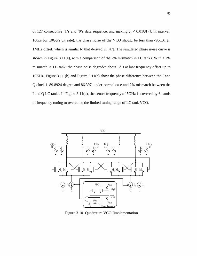
85
of 127 consecutive ‘1’s and ‘0’s data sequence, and making σj < 0.01UI (Unit interval,
100ps for 10Gb/s bit rate), the phase noise of the VCO should be less than -90dBc @
1MHz offset, which is similar to that derived in [47]. The simulated phase noise curve is
shown in Figure 3.11(a), with a comparison of the 2% mismatch in LC tanks. With a 2%
mismatch in LC tank, the phase noise degrades about 5dB at low frequency offset up to
10KHz. Figure 3.11 (b) and Figure 3.11(c) show the phase difference between the I and
Q clock is 89.8924 degree and 86.397, under normal case and 2% mismatch between the
I and Q LC tanks. In Figure 3.11(d), the center frequency of 5GHz is covered by 6 bands
of frequency tuning to overcome the limited tuning range of LC tank VCO.
VDD
M 2 M1 M2M 1
CKI+ CKI-
I1 I2
M2M 1M2 M1
CKQ-CKQ+
I1I2
VBIAS
VBIASVDD
Vref Peak Detector
CKI+
CKI-
Figure 3.10 Quadrature VCO Iimplementation

86
Figure 3.11 PSS Analysis of the VCO: (a) Phase Noise Simulation of the VCO, (b) Phase Mismatch between the I/Q Clocks of the VCO
(a)
(b)
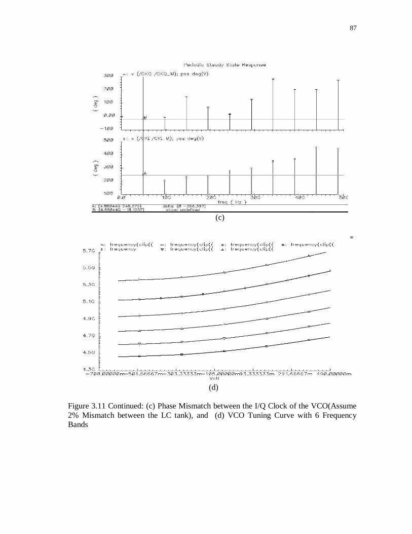
87
Figure 3.11 Continued: (c) Phase Mismatch between the I/Q Clock of the VCO(Assume 2% Mismatch between the LC tank), and (d) VCO Tuning Curve with 6 Frequency Bands
(c)
(d)

88
Due to process, voltage and temperature (PVT) variations the amplitude of the VCO
output is not well controlled. To minimize this issue, an automatic amplitude control that
uses a peak detector [48] and a single-stage differential pair amplifier which adjusts the
tail current of the LC tank maintains constant VCO amplitude. The VCO’s output
amplitude can also be externally adjusted through an array of programmable current
sources.
The switching in or out of the MIM capacitor bank is controlled by a successive
approximation register (SAR) block. Since the accumulation varactor is designed by
putting NMOS transistor into an N-well, it can not be simulated directly as the inversion
mode varactor which can use the transistor model. The varactor simulation is made easy
by a convenient model which is shown in Figure 3.12 (a). The model use a PMOS
transistor which has the same size as the NMOS transistor in the varactor, and the VBG is
the bandgap voltage source (around 1.2V); the bulk of the PMOS transistor is considered
as the tuning voltage input. The simulated varactor curve and the measured varactor
curve are compared in Figure 3.12(b); deviations are less than 10% at 75°. The
component values are summarized in Table III.5.
TABLE III.5 COMPONENT VALUES OF THE QVCO IN Figure 3.8(a)
M1 16u/0.18u Mtail (I2) 250u/0.54
M2 8u/0.18u Mtail (I1) 54/0.5u
Inductor 0.9nH Varctor 0.8 to 1.5pF

89
Figure3.9 Varactor simulation Model.
Figure 3.12 Varactor Model and Simulation: (a) Varactor Model and (b) Varactor Capacitance versus Input Gate Voltage
(b)
- +- +VB
VBG
VtuneC+
(a)
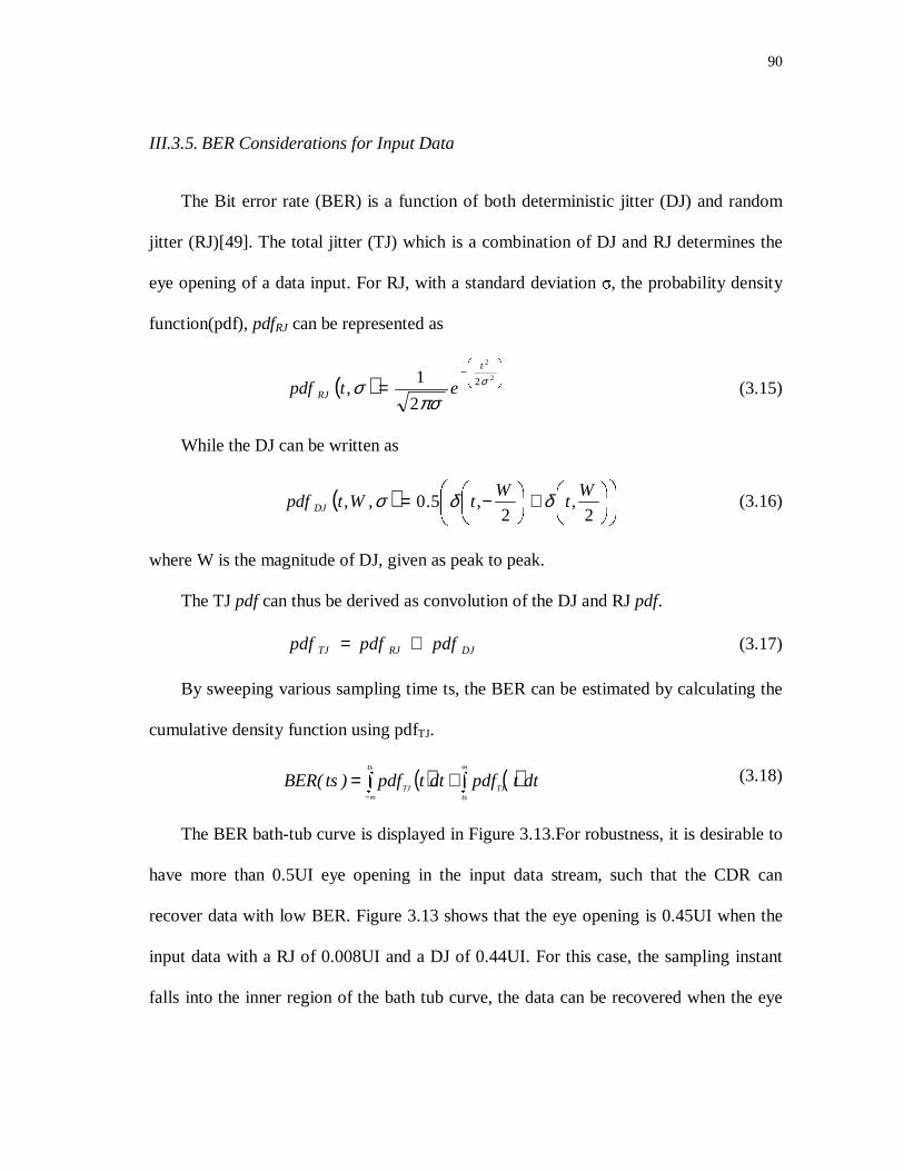
90
III.3.5. BER Considerations for Input Data
The Bit error rate (BER) is a function of both deterministic jitter (DJ) and random
jitter (RJ)[49]. The total jitter (TJ) which is a combination of DJ and RJ determines the
eye opening of a data input. For RJ, with a standard deviation σ, the probability density
function(pdf), pdfRJ can be represented as
( ) −
=2
2
2
2
1, σ
πσσ
t
RJ etpdf (3.15)
While the DJ can be written as
( ) + −=2
,2
,5.0,,W
tW
tWtpdf DJ δδσ (3.16)
where W is the magnitude of DJ, given as peak to peak.
The TJ pdf can thus be derived as convolution of the DJ and RJ pdf.
DJRJTJ pdfpdfpdf ⊗= (3.17)
By sweeping various sampling time ts, the BER can be estimated by calculating the
cumulative density function using pdfTJ.
( ) ( )dttpdfdttpdf)ts(BERts
TJ
ts
TJ ∫∫ ∞
∞−
+= (3.18)
The BER bath-tub curve is displayed in Figure 3.13.For robustness, it is desirable to
have more than 0.5UI eye opening in the input data stream, such that the CDR can
recover data with low BER. Figure 3.13 shows that the eye opening is 0.45UI when the
input data with a RJ of 0.008UI and a DJ of 0.44UI. For this case, the sampling instant
falls into the inner region of the bath tub curve, the data can be recovered when the eye

91
opening is over 0.44UI with a BER < 10-12. For the combination of 0.02UI RJ and 0.6 UI
DJ, the eye opening is only 0.16UI for a BER < 10-12, which is very tough even for the
CDR to recover data with BER < 10-12.
Figure 3.13 BER Bath-tub Curve as Function of Different DJ & RJ Combinations
III.3.6. Some Simulation Results of the CDR Loop
To verify the function of the designed CDR circuit, the 10Gb/s PRBS data input are
distorted by adding over 0.28UIpp ISI jitter. The CDR can regenerate the input data and
the peak to peak jitter is less than 4ps, which is less than 0.05UIpp. The eye diagram of
the input data and the recovered data of the CDR device is shown in Figure 3.14 (a) and
0.46UI
0.44UI
0.46 UI
0.44UI

92
Figure 3.14(b); Figure 3.14(c) demonstrates the pull-in process of the CDR, the
recovered clock of the CDR converges to the frequency of 5GHz, which is half rate of
the input date rate, the rms jitter of the clock is 0.96ps. In the next section, experimental
results are described in detail.
Figure 3.14 Top Level Simulation Results: (a) The Eye Diagram of the Input PRBS Data with a Total Jitter (TJ) of 28.1ps, (b) The Eye Diagram of the Recovered Data by the CDR,with a TJ of 3.17ps
(b)
(a)

93
Figure 3.14 Continued: (c) The Pull-in Process of the CDR Circuit
III.4. Experimental Results
The chip was fabricated in a 0.18µm, 1P6M CMOS process through the MOSIS
educational service; Figure 3.15 shows a micrograph of the CDR, which is pad-limited
and occupies 2 x 2 mm2 chip area with the on-chip loop filter included. The entire
characterization test is performed at room temperature. BER and jitter tolerance were
performed by using an Anritsu MP1763C 12.5GHz pattern generator, Anritsu 1764C
12.5GHz error detector, and Agilent 71501C jitter analysis test systems.
III.4.1. Printed Circuit Board (PCB) Design
A four layers PCB is designed and fabricated for the characterization of the
prototype chip. A photo of the fabricated PCB is shown in Figure 3.16. The reference

94
clock differential inputs, data inputs, and recovered clock outputs, recovered data
outputs are routed as co-planar waveguide (CPW) in order not to cause serious loss to
high speed signals. All the high speed signal tracks are terminated using 50 ohms load.
Several potentiometers (variable resistors) are used to adjust the bias of the CDR
devices.
Figure 3.15 Chip Microphotograph
The analog and digital power supplies are separated in order to reduce the effect of
digital switching noise coupled into the analog power supply. The VCO and VCO buffer
are powered using a separate voltage regulator to reduce the power pulling of the VCO.
VCO
Lock Dete
PD PFD
Out
Filter Capacitors

95
Figure 3.16 The PCB to Test the Prototype IC
Special attention is paid in designing the PCB by using Protel CAD software; to
name a few:
1) The CPW traces are 10mil wide typically; the differential pair traces are 11mil wide
separated.
2) Enough vias are placed for ground plane for good conduction.
3) Fill ground plane near the high speed traces as symmetrical geometry, such that the
differential signals have the same environments and hence good matching.
4) Adding decoupling caps near the chip to reduce the ground bounce noise.
5) ESD power and ground are routed separately.

96
6) Power traces are made as wide as possible, in order to improve the thermal
performance, tear-drop vias are placed on both power and ground.
7) All the transmission lines avoid the use of right angle to reduce the reflection effect.
As shown in the photo of the fabricated PCB, the transmission lines bend smoothly
instead of using right angles.
8) All the 0805 package chip capacitor are replaced using smaller SMT package such as
0402 and 0603 package to reduce parasitic capacitance.
9) When soldering SMA connector, the SMA pins are cut shorter to reduce the parasitic
effect and improve the signal integrity.
III.4.2. Test Equipments Setup
Test equipments setup, the list of the test equipments used are listed below:
1) Agilent 71501D jitter analyzer
2) Agilent 70843C Error Detector
3) HP Signal generator 83752A for reference clock generation.
4) Agilent 86100C Oscilloscope(>40G/s)
5) Anritsu PRBS pattern generator MP1764C
6) HP Power supply
The test diagram is shown in Figure 3.17.

97
Figure 3.17 Measurements Setup Diagram
The test PCB board for the prototype chip is connected in the setup shown in Figure
3.18. The input data at 9.9532Gb/s is generated by the Anritsu MP7164C pattern
generator; then the data is passed through the measurement cable and connectors to the
data input SMAs of the PCB board. The recovered data is connected to the Agilent
70843C to perform Bit error rate(BER) analysis. Also the data can be passed to the high
speed sampling oscilloscope for measuring the eye diagram. The jitter tolerance and
jitter transfer measurement is similar; the only difference is that the Oscilloscope is
replaced by the Agilent 71501D jitter analyzer.

98
Figure 3.18 Photo of a Typical Equipment Setup to Test the Prototype IC
III.4.3. Measurements Results of the Prototype IC
III.4.3.1. Measurements by Adding ISI in the Input Data
In 10-Gigabit Ethernet (10GE) applications, the wideband jitter in the serial inputs
typically adds the difficulty of the CDR device to recover the clock. A good way to
measure the performance of the CDR device is to add inter-symbol interference (ISI) to
the input data, the ISI induced jitter is a wideband jitter which can test roughly the jitter
tolerance of the CDR.

99
By passing the input data to a 9 inches PCB traces, excess ISI is included in the data
input, the horizontal eye closure is around 0.54UI. Figure 3.19 shows the eye diagram of
a stressed 215 –1 input PRBS data and the recovered data at 9.953Gbps. Even if the
horizontal eye closure4 is 0.54UI, the device can still recover the data with a BER < 10-
12. The RMS-jitter of the recovered data is less than 0.74ps with a 215 –1 PRBS pattern
for input data with 150mVpp single-ended amplitude. Jitter statistics are shown in Figure
3.20. It can be shown that the ISI jitter in the input data pattern is around 54.5ps while in
the recovered data the ISI jitter is only 13.3ps peak to peak, which shows that the CDR
works properly with acceptable jitter tolerance for 10 Gigabit Ethernet applications. The
active inductor peaking in the buffer chain contributes to help equalize the input data
signal.
The waveform of the recovered clock is shown in Figure 3.21 with a peak to peak
jitter of 8ps which is less than 0.08UI and conforms to the SONET jitter generation
specification( < 0.1UIpp). Jitter tolerance is tested by passing the data pattern generated
from the pattern generator to the device under test (DUT), the recovered data is sent to
BERT tester for BER test. There is no loop back testing through the transmitter. As
shown in Figure 3.20, for an input signal of 150mVpp single-ended, a high frequency
jitter tolerance greater than 0.3 UIpp is achieved (at 80MHz of sinusoidal jitter frequency,
the jitter tolerance is 0.31UIpp), which confirms that, for 0.5UI eye closure at the input
4 The stressed data is generated by passing the data out of pattern generator to 9 inches FR4 PCB trace.

100
.
Figure 3.19 Eye Diagram for Input Data PRBS 2^15-1 with TJ of 54.5ps
Figure 3.20 Eye Diagram of Recovered Data with Input Data Shown in Figure 3.19

101
Figure 3.21 The Recovered Half Rate Clock with 8ps Peak-to-peak with PRBS with a Pattern Length of 231-1
Figure 3.22 CDR Jitter Tolerance Measurements
0.10
1.00
10.00
100.00
1.00E+02 1.00E+03 1.00E+04 1.00E+05 1.00E+06 1.00E+07 1.00E+08
OC-192 Mask
DUT
Instrument Limit
Jitter Frequency (Hz)
Jitt
er A
mpl
itude
(U
I pp)

102
data due to ISI distortion, the CDR can still recover the data correctly. The CDR exceeds
the SONET OC-192 jitter tolerance mask with over 100% margin for jitter frequency
higher than 10MHz; for jitter frequency lower than 2MHz, the CDR exceeds the jitter
tolerance test limit of the equipment used, where the data input is a 231-1 PRBS pattern.
III.4.3.2. Jitter Tolerance Measurement
The jitter tolerance specification in SONET OC-192 standard defines the jitter
criteria to measure the ability of the CDR device to recover the input data with an in-
band jitter ranging from 50KHz to 80MHz. It is in general measured by adding
sinusoidal jitter (<80MHz) to the input data until -1dB loss in the signal power is
reached. In our measurement, only several measurements are based on BER of 10-12
because it is very time consuming. In many cases, a BER of 10-10 measurement can be
performed to check the functionality of the prototype IC. Measurement result shown in
Figure 3.22 shows that the device passes the jitter tolerance test , with a slightly passing
at around 1MHz frequency; That is due to the measurement limit of the test equipment.
III.4.3.3. Jitter Transfer Measurement
As discussed in previous sections, SONET jitter transfer specification defines the
jitter peaking performance of the CDR devices when used in a chain of repeaters in
telecommunication products. A jitter peaking of less than 0.1dB is recommended in

103
SONET OC-192 specification. The jitter transfer measurement is done by phase
modulating the input data and measuring the phase modulation in the recovered clock.
The jitter transfer curve is similar to a single-pole low pass filter response, i.e., it shows
a -20dB rolling off until the 3dB bandwidth frequency is reached. The measurement
result is shown in Figure 3.23, which shows that the jitter transfer bandwidth (corner
frequency) is 6.2MHz, and the jitter peaking is 0.07dB(less than 0.1dB defined in the
SONET standard), thus it does not meet the SONET standard for the jitter transfer
specification of 120KHz. However, as pointed out in [5], the jitter transfer characteristic
can be shaped by a jitter attenuator PLL to shape the jitter transfer bandwidth of the
clock recovered by the CDR.
Figure 3.23 Jitter Transfer Measurement of the CDR Device
-20.00
-10.00
0.00
1.00E+02 1.00E+03 1.00E+04 1.00E+05 1.00E+06 1.00E+07 1.00E+08
OC-192 Mask
DUT

104
III.4.3.4. Jitter Generation Measurement
The jitter generation measurement is performed without adding external jitter at the
input data, and measure the CDR device intrinsic jitter (or Phase noise). The limitation
of the bang-bang CDR is that due its nonlinear nature. Even if the CDR loop is locked,
the control voltage of the VCO fluctuates slightly, which is unlike a linear phase detector
CDR, thus potentially bang-bang CDR has worse jitter generation performance than a
linear phase detector CDR.
Figure 3.24 Frequency Spectrum of the Recovered Clock

105
The measurement of the spectrum and phase noise of the recovered clock when the CDR
device is locked are shown in Figure 3.24 and Figure 3.25, respectively.Notice that, the
measured phase noise is a little bit worse than the simulated VCO phase noise at 1MHz
offset, the reason probably is the lack of the accuracy when modeling the inductor. Also
long interconnection in the layout of the chip limits the performance of the whole chip.
Figure 3.25 Phase Noise Plot of the Recovered Clock
To test the spectrum purity of the recovered clock, an 80MHz sinusoidal jitter with
0.32UIpp amplitude is applied to the data input by the pattern generator, the clock
spectrum is shown in Figure 3.26. The attenuation of the 80MHz sinusoidal jitter is
better than -42dB.

106
Figure 3.26 Measured Attenuation of 80MHz of Sinusoidal Jitter, 0.32UIpp
III.4.3.5. Return Loss Measurement
Return loss is the ratio, at the junction of a transmission line and a terminating
impedance or other discontinuity, of the amplitude of the reflected wave to the amplitude
of the incident wave [50]. The return loss value describes the reduction in the amplitude
of the reflected energy, as compared to the forward energy. Typically in a transmission
line, return loss is defined as

107
0
010log20
ZZ
ZZRL
src
src
+−
= (3.19)
where Zsrc and Z0 are the impedance toward the source and the load respectively. In our
prototype, Z0 is selected as 50 ohm to match the prevalent of the industry PCB
vendor.Figure 3.27 shows the return loss of the input buffer, it is less than -13dB at
5GHz.
III.4.3.6. Pull-out Range Measurement
After the CDR locks to the input data at 9.953Gb/s rate, the phase detection loop
can maintain lock even if the input data rate changes from 9.947Gb/s to 9.958Gb/s
without going to frequency acquisition loop, which shows that the pull-out range of the
phase detection loop is over 1100ppm.
III.4.3.7. Summary of the Measurements
Including the buffers, the chip consumes 290mW with a 1.8VPower supply. The
chip is packaged in a 5 x 5 mm QFN package. Multiple pins are assigned to both power
supply and ground to minimize the crosstalk effect. Performance of the chip is
summarized in Table III.6, which shows that the proposed implementation consumes
less power than previously reported solutions, except for the one reported in [10] which
does not account the power consumption of the buffers. If the four on-chip inductors are

108
replaced with two symmetric inductors, the chip area can be reduced even further. The
jitter tolerance performance of the chip is approaching or even better than reported
implementation using better CMOS technologies such as 0.11um CMOS.
Figure 3.27 Measured Return Loss of the Input Buffer (< -13dB at 5GHz)
III.4.3.8. Summary of the Measurements
Including the buffers, the chip consumes 290mW with a 1.8VPower supply. The
chip is packaged in a 5 x 5 mm QFN package. Multiple pins are assigned to both power
supply and ground to minimize the crosstalk effect. Performance of the chip is

109
summarized in Table III.6, which shows that the proposed implementation consumes
less power than previously reported solutions, except for the one reported in [10] which
does not account the power consumption of the buffers. If the four on-chip inductors are
replaced with two symmetric inductors, the chip area can be reduced even further. The
jitter tolerance performance of the chip is approaching or even better than reported
implementation using better CMOS technologies such as 0.11um CMOS.
III.5. Conclusions
A fully integrated 10-Gb/s CDR is implemented in a 0.18µm CMOS process. The
design uses half rate architecture due to the relative low ft (50GHz) of the CMOS process
used. By using a new loop filter and charge pump configuration, the chip integrates all
the components on-chip including the integration capacitor. Improved charge pump
architecture with source degeneration, VCO with amplitude tuning and multiplexer
scheme in double edged DFFs are the other techniques adopted to enhance the chip
performance.
The CDR can recover data with a BER less than 10-12 when the input eye closure is
slightly above 0.5UIpp(Horizontal eye closure) and the recovered clock with peak to peak
jitter less than 0.1UIpp.The CDR also exceeds the OC-192 jitter tolerance mask with high
frequency jitter tolerance over 0.31UIpp. To the best our knowledge, this reported
implementation is the first fully integrated, PLL based 10Gb/s CDR in the literature.

110
TABLE III.6 SUMMARY OF THE MEASUREMENT RESULTS FOR 215-1
[10] [12] [51] [30] This work[52]
Technology
0.18µm CMOS
0.18µm CMOS
0.11um CMOS
0.13um CMOS
0.18µm CMOS
Power dissipation
91mW+buffer power
400mW 311mW 980mW(in
cluding TX) 290mW(buffer
included)
Chip size(mm2)
1.75x1.55 1.95x1.5 2.9x1.6(for
two channels sharing PLL)
3x5(the transceiver)
< 2x2
Input Bit
rate(Gb/s) 9.9532 9.9532 9.9532 9.9532 9.9532
RMS/peak-to-peak
clock Jitter when
locked to input data
0.8ps/9.9ps pk-pk(locked to PRBS 223-
1)
1.2ps/8ps pk-pk(locked
to 2.5GHz sinusoidal)
NA
1.1ps/8.3ps pk-pk(locked
to 231-1 PRBS)
1.2ps/8ps pk-pk(locked to 231-1
PRBS)
Frequency
detection Included
Not included
NA Included Included
Jitter tolerance
Not passing ~0.15UIpp at high
frequency
~0.2UIpp at high
frequency 0.35UIpp
> 0.31UIpp for high frequency
JTOL BER 10-9 NA <10-14 <10-12 < 10-12
Pull-out range of the phase detection loop only
NA NA 500ppm NA >1100ppm
Supply voltage
1.8V 1.8V 1.2V 1.2V 1.8V. ± 10%

111
IV. A MULTI-GIGABIT/S CLOCK DATA RECOVERY ARCHITECTURE USING
AN ADAPTIVE BANG-BANG CONTROL STRATEGY
IV.1. Introduction
Demand for low cost SerDes ICs have been boosted due to the widespread use of
SONET/Gigabit Ethernet network and chip-to-chip interface such as PCI-Express
(PCIe), Serial ATA (SATA) and Fiber channel standard applications. Among all these
applications, clock data recovery (CDR) is one of the key design components. With the
increasing demand for higher bandwidth and large scale integration, CMOS
implementation is now a design trend for predominant products. The higher bandwidth
requirements (over 10GHz) and the relatively low transistor’s ft make the bang-bang
phase detector based clock recovery products dominate the current market compared
with the Hogge phase detector CDR products [51].
A linear phase detector usually outputs a pulse whose width is proportional to the
phase error, and is a percentage of the data period; hence at a data rate greater than
10Gb/s, it is very difficult to process the phase error pulse even if state of the art deep
submicron CMOS technologies are employed. The bang-bang phase detector is based on
a digital processing of the phase information in a nonlinear way.
In spite of these compelling advantages of the bang-bang CDR loop, all of the
reported PLL based CDR loops use a fixed bang-bang control setting to perform phase
detection. Under such fixed configurations, when tracking high frequency sinusoidal
jitter, the CDR experiences slew-rate limited tracking process and the jitter tolerance

112
performance is degraded due to the limited equivalent bandwidth of the bang-bang loop.
In this section, a new CDR architecture with slope-overload prediction and adaptive
bang-bang control mechanism to maximize its jitter performance is proposed [46]. A
digital predictor helps to optimize the loop bandwidth based on current and previous data.
The main idea is that, by predicting the timing information of the CDR adaptively, the
clock information can be more accurate than classical CDR architecture.
IV.2. Description of the Classic Bang-bang CDR Architecture
IV.2.1. Existing CDR Architecture
IV.2.1.1. 1st Order Bang-bang CDR
The 1st order bang-bang CDR can be represented by the block diagram shown in
Figure 4. 1. The incoming data has a nominal frequency fnom and an offset frequency δf. As discussed in [53], the data phase φd (the sum of phase jitter and the phase shift
caused by δf) and VCO phase φv generate the phase error φe ; the error phase is digitized
by the two-level phase comparator (detector) at the clock rate of the VCO output. The
digitized phase error information is firstly attenuated by a factor α and then pulse
modulates the VCO to track its phase with the input data phase. Evidently this phase
tracking is a non-linear process due to the inherently non-linear phase detector. If the
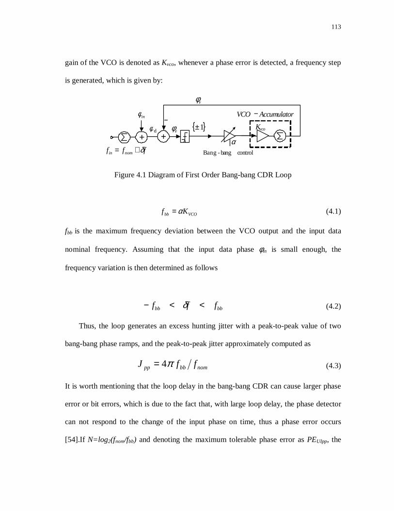
113
gain of the VCO is denoted as Kvco, whenever a phase error is detected, a frequency step
is generated, which is given by:
+vcoK
AccumulatorVCO −
αBang -bang controlfff nomin δ+=
1±eφ
vφ
+
inφ
dφ
Figure 4.1 Diagram of First Order Bang-bang CDR Loop
VCObb Kf α= (4.1)
fbb is the maximum frequency deviation between the VCO output and the input data
nominal frequency. Assuming that the input data phase φin is small enough, the
frequency variation is then determined as follows
bbbb fff <<− δ (4.2)
Thus, the loop generates an excess hunting jitter with a peak-to-peak value of two
bang-bang phase ramps, and the peak-to-peak jitter approximately computed as
nombbpp ffJ π4= (4.3)
It is worth mentioning that the loop delay in the bang-bang CDR can cause larger phase
error or bit errors, which is due to the fact that, with large loop delay, the phase detector
can not respond to the change of the input phase on time, thus a phase error occurs
[54].If N=log2(fnom/fbb) and denoting the maximum tolerable phase error as PEUIpp, the

114
loop delay (LD) should satisfy:
( ) UIppN PELD 12 −≤ (4.4)
Assuming a maximum jitter of 0.25 UIpp, and N=10 for reasonable bandwidth, the
loop delay should be less than time required by 255 cycles. In this paper, the loop delay
is selected to be less than the time required by 16 cycles for ease of implementation,
stability, and jitter tolerance considerations.
Despite the straightforward implementation of the 1st order bang-bang loop, it has
the limitation of limited frequency tracking range. In order to increase the locking range
of the bang-bang loop, besides the bang-bang branch, an integral branch can be added to
extend its frequency range, and hence the jitter performance of the CDR can be
improved further.
IV.2.1.2. 2nd Order Bang-bang Loop
The block diagram of a 2nd order Bang-bang loop is shown in Figure 4. 2. The
contribution to the phase control of both paths α and integrator of (1/τ)Σ in a time period
equal to the bit period Tbit occurs when α= Tbit/2τ; therefore, the loop stability factor ξ is
defined in [53].
12 >>=
bitT
ατξ (4.5)

115
where Tbit is the bit period, and τ is the time constant of the integrator used in the loop
filter. It is well known in control systems that to guarantee stability the loop must be
designed such that ξ>>1 [53]. Because of the overload limited (Slew limited) characteristic of the nonlinear phase
tracking loop, the limit for the effective bandwidth of the CDR loop (BW) follows the
following equation (4.6). It can be expressed in a simplified form as follows [22]
pkUIpk
bbp
Jitter
fKBW
−
= (4.6)
where JitterUIpk-pk is the peak to peak jitter amplitude in a unit interval (UIpk-pk) at the
frequency of interest; Kp is the fitting parameter which accounts for the delay of the
phase detector and is usually approximated as 1.2 when input sinusoidal jitter amplitude
is around 0.06UIpk-pk, and fbb is the bang-bang frequency step. According to (4.6), the
bandwidth is inversely proportional to the input jitter amplitude, which is a result of the
nonlinear nature of the binary PD. This statement can be confirmed by the describe
function obtained in Appendix C.
An ideal comparator is described as Vout=D*Sign(Vin), and the describe function is
found in the Appendix C as DF=4*D/ πA, where A is the amplitude of the input
sinusoidal signal Vin ;and D is the signal amplitude at the PD output. If the DF is
combined with the linear part of the system, as expected, it is shown that the resultant
loop bandwidth is inverse proportional to the input jitter amplitude; details of this
derivation are given in Appendix C.

116
+vcoK
AccumulatorVCO −
αBang-bang controlfff nomin δ+=
1±eφ
vφ
+
inφ
dataφ
τ1
Figure 4.2 Diagram of a Typical 2nd Order Bang-bang CDR
IV.2.1.3. Slope Overload or Slew-rate Limited Process in Phase Tracking
For simplicity, let us assume that the frequency difference between the incoming
data and the VCO is small, and that( ) ( )0mod2sin φπφ += tfAt UId , where AUI is the
maximum jitter amplitude measured in peak-to-peak unit intervals, fmod is the sinusoidal
modulation frequency, and φ0 is the initial phase for the sinusoidal jitter input. If the
CDR tracking speed is not as fast as the input data phase changes, then jitter induced
slope-overload or slew-rate limited process appears, as depicted in Figure 4.3. The slew
rate limited process is very similar to the case of the over-damped unit response of a
linear system.
The slew-rate (or slope-overload) occurs if the incoming phase variation is larger
than the VCO phase variation; this condition is mathematically expressed as
( )( ) bbUId fAftdt
d ππφ 22max mod >= (4.7)

117
Figure 4.3 Slope-overload (or Slew-rate Limited) Phase Tracking Process
Under this condition, the peak-to-peak jitter of the hunting jitter given in (4.3) is
larger compared with the case of non-slew-rate limited process. According to (4.7), the
slew rate limiting also depends on the product of both the jitter frequency and the peak-
to-peak jitter amplitude when considering a sinusoidal jitter, which is the toughest
condition for a typical CDR device to track.
IV.3. Proposed CDR Architecture
The conventional bang-bang CDR is based on constant bang-bang frequency step to
control its loop dynamics. Recently [54],[55] added some programmability to the bang-
bang control to optimize the loop bandwidth; in those approaches, the charge pump
current sources or the buffer amplifier gain are adjusted to change the loop dynamics.
The 1st order bang-bang loop bandwidth can be varied in four steps, i.e., 2-13, 2-14, 2-15, or
2-16 of the nominal data rate. The bang-bang control in a strict sense still belongs to a
constant bang-bang control category and can not track the high frequency jitter because
dφ
vφ

118
the equivalent CDR loop bandwidth is inversely proportional to the peak to peak input
jitter amplitude. For larger input data jitter, the effective bandwidth is reduced, and thus
its jitter tracking capability decreases as well. In many cases, due to the presence of the
unknown high frequency jitter, it is necessary to include a top level controller or CPU to
configure the PLL bandwidth for the IC through a higher level protocol. However, by
adopting an adaptive control of the bang-bang CDR can lead to a more robust
performance across different high frequency jitter of interest.
If the CDR bandwidth is not large enough, then there is definitely the slew-rate
limiting process and the corresponding peak-to-peak jitter is larger than that without
severe slope-overloading case. Even if there is no slew-rate limiting process, the
nonlinear nature of the bang-bang CDR loop shows hunting jitter at its steady state and
the phase detector still outputs alternate high and low pulses, for the first order loop, that
is equivalent to a clock pulse with close to 50% duty cycle. With a frequency change in
data( df∆ ), and delta frequency variation in the VCO (Vf∆ ), a frequency step response
can be derived similar to linear system response. Shown in Figure 4.4, the top graph is
the case for a slope-overload (slew-rate limiting); and the bottom trace shows a slope-
overshoot case where the CDR loop bandwidth is too small. Under both situations, the
resultant tracking phase error is not optimized when the CDR loop operates in the steady
state.
If the slope-overload or the slew-rate limiting process are detected or predicted in
advance, then the loop dynamics can be varied according to the input jitter characteristic
and hence the jitter tolerance performance can be greatly improved. In the following

119
sections, an architecture with adaptive bang-bang control is presented to tradeoff the
design of slew-rate limiting and steady state jitter generation.
Referring back to the diagram in Figure 4.3, the digitized phase error output is
plotted in Figure 4. 5. If the slope of the top trace( data phase) changes fast, there is
constant high or low signal at the digitized phase error output, which means that there is
slew-rate limiting occurrence. If looking more carefully at the digitized phase error
output, it can be concluded that there is similarity between the architecture in Figure 4.3
with the conventional Sigma-delta modulator or delta modulator. That is the basic
starting point why the adaptive modulation is adopted in the proposed bang-bang CDR
design.
IV.3.1. CDR Architecture with Adaptive Bang-bang Control
A formal quantitative definition of slope overload in the CDR tracking process is
difficult. A succession of more than two like bits is a reasonable criterion. Then the
target is to find a method to detect or predict slope overload or slew rate limiting in the
phase tracking process and then adaptively adjusts the bang-bang loop bandwidth when
needed.

120
Figure 4.4 The Phase Tracking Slew Rate Limiting Process: (a) Slope Overload Caused by Limited Bandwidth; (b) Slope Overshoot Caused by Too Small Loop Bandwidth
0 1000 2000 3000 4000 5000 6000-0.1
0
0.1
0.2
0.3
0.4
0.5
0.6
0.7
0.8
0.9
(a)
df∆
Vf∆
(a)
0 1000 2000 3000 4000 5000 6000-0.5
0
0.5
1
1.5
2
2.5
3
3.5
4
4.5
df∆
Vf∆
(b)
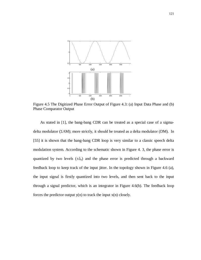
121
Figure 4.5 The Digitized Phase Error Output of Figure 4.3: (a) Input Data Phase and (b) Phase Comparator Output
As stated in [1], the bang-bang CDR can be treated as a special case of a sigma-
delta modulator (Σ∆M); more strictly, it should be treated as a delta modulator (DM). In
[55] it is shown that the bang-bang CDR loop is very similar to a classic speech delta
modulation system. According to the schematic shown in Figure 4. 3, the phase error is
quantized by two levels (±δn) and the phase error is predicted through a backward
feedback loop to keep track of the input jitter. In the topology shown in Figure 4.6 (a),
the input signal is firstly quantized into two levels, and then sent back to the input
through a signal predictor, which is an integrator in Figure 4.6(b). The feedback loop
forces the predictor output y(n) to track the input x(n) closely.
0 500 1000 1500 2000 2500 3000-0.5
0
0.5
0 500 1000 1500 2000 2500 3000
-1
-0.5
0
0.5
1
(a)
(b)

122
nδ±)(nx
)n(y
(a)
1±)(nx
)n(y
(b)
Figure 4.6. Delta Modulator: (a) Standard Delta Modulation Diagram (Similar to DPCM) and (b) An Implementation of DM Encoder
The concept of first order predictor can be extended to higher order; in Figure 4.7
and 4.8 an adaptive bang-bang CDR diagram for 1st and 2nd order CDR, respectively, are
presented. Actual and previous values of the quantized phase error are used to control
the bang-bang attenuating factor α, such that the loop bandwidth can then be
dynamically adjusted according to the phase variations of the input data.

123
( )Dataφ vcoK
rAccumulatoVCO−
1−z
α
1−z
Figure 4.7 1st Order Binary CDR with Adaptive Control
vcoK
rAccumulatoVCO−
1−z
α
1−z
Figure 4.8 2nd Order Binary CDR with Adaptive Bang-bang Control
In order to use adaptive delta modulation (ADM) scheme in our CDR system, the
architecture of ADM should be addressed first. In [54], a constant factor adaptive delta
modulation with a one-bit memory is proposed. Denoting the quantizer output as b(n),
and its previous memory is b(n-1), and defining the current quantization step size as δ(n),
and its previous step size is δ(n-1) then

124
( ) ( )( ) −≠−
−=−=
)1()(1
)1()(1
2
1
nbnbifnM
nbnbifnMn
δδ
δ (4.8)
where M1 and M2 are the step sizes of the quantizer.
In the proposed implementation, two bits of memory of the phase error are adopted
for robust slope overload prediction, which is similar to the approach suggested in [56]-
[57]. The phase error output generates four different results: when successive three or
more bits of the same level (high or low) are output from the phase detector, the
condition is defined as slope overload; if two consecutive phase outputs have the same
level, and differ from the foremost history, this is classified as a semi-overload condition;
while both the previous output and the foremost memory differ from the current phase
detector output, the condition is classified as sign reversal; when the current output and
previous two output alternate polarity, we denote this condition as “alternate polarity”.
These conditions are mathematically described as follows:
( )
( )( )( )( ) −≠−≠−
−=−≠−−≠−=−
−=−=−
=
);2()1()(1
);2()1()(1
);2()1()(1
);2()1()(1
4
3
2
1
nbnbnbifnM
nbnbnbifnM
nbnbnbifnM
nbnbnbifnM
n
δδδδ
δ (4.9)
For this implementation, M1 is selected as 2.0, M2 is 1.5, and M3 is 0.5, while M4 is
0.75 for easy installation of the current source arrays. M1 = 2.0 can be realized by using
logic left-shift one bit ( << 1); M3 thus can be right-shifted by 1 bit ( >>1); and M2 is the
sum of left-shift 1 bit and right-shift 1 bit; M4 is the sum of right-shift 1 bit and right
shift 2bits of the operands.

125
IV.3.2. Circuit Implementation of the Adaptive Bang-bang Control
Table IV.1 shows the adaptive control of the frequency step size. B(n) is the actual
phase detector output, and B(n-1) and B(n-2) are one and two cycle delays of the B(n).
Figure 4.9a shows an implementation of the state machine of adaptive bang-bang
control. The state is described as S[1:0], which corresponds to the two bits of B(n-1) and
B(n-2); there are four possible states “00”,”01”,”10” and “11”. The output of the Mealy
state machine is separated with the incoming bit by a slash “/”, for example, “0/11”, the
incoming bit is “0”, the output is “11”. The step size of the bang-bang control can be
represented as:
[ ] −⊕−=
−⊕=
)2()1(]0[_
;)1()(1_
nBnBsizeStep
nBnBsizeStep (4.10)
where ⊕ denotes XOR logic function, and output denotes logic inversion. The adaptive
logic diagram is depicted in Figure 4. 9b.
As a reference design, a variable gain amplifier design with source degeneration,
shown in Figure 4.10, can be used as the bang-bang control block (denoted as α) in
Figure 4.7 and Figure 4. 8.

126
TABLE IV.1.STEP SIZE ADJUSTMENT FOR THE PROPOSED CDR
B(n) B(n-1) B(n-2) State Step size
-1 1 -1 Alternate polarity 0.75
1 -1 1 Alternate polarity 0.75
-1 1 1 Sign reversal 0.5
1 -1 -1 Sign reversal 0.5
-1 -1 1 Semi-overload 1.5
1 1 -1 Semi-overload 1.5
-1 -1 -1 Overload 2
1 1 1 Overload 2
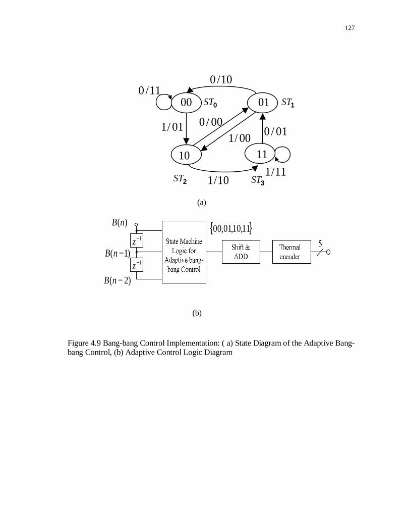
127
Figure 4.9 Bang-bang Control Implementation: ( a) State Diagram of the Adaptive Bang-bang Control, (b) Adaptive Control Logic Diagram
00 01
1110
11/0
11/110/1
01/1 00/000/1
01/0
10/0
0ST 1ST
2ST 3ST
(a)
1−z
1−z
)(nB
)1( −nB
)2( −nB
11,10,01,00
(b)

128
Figure 4.10 Variable Gain Amplifier Using Source Degeneration
IV.4. Performance Comparison: A Statistical Approach
In this section, we will derive the steady state probability of the adaptive CDR
comparing with that of classical BB CDR using Markov chain modeling and statistical
analysis.
The discussion of a Markov chain can be found in [58]. In general, a Markov chain
is a sequence of random variables X1,X2,X3… with the Markov property, namely that,
given the present state, the future and past states are independent[59]. Formally, the
conditional probability is defined as the probability of some event, given the occurrence

129
of some other state such as Xn, written as. In Figure 4. 8, the bang-bang control is in
essence a finite state machine. If the machine is in state STn at time n, then the
probability that it moves to state STn+1 at time n+1 depends only on the current state.
Thus the state machine can be explained using a Markov chain. Simply we have:
( ) ( )nnnnnn xSTxSTxSTxSTxST ====== ++ 1111 Pr,..,Pr (4.11)
where x and xn are the possible values of variable STn.
The possible values of STn from a countable set S called the state space of the chain.
In our analysis, because for each state change in the state machine, the phase of the
recovered clock changes accordingly, it is reasonable that the possible phases of the
recovered clocks are modeled as a Markov chain, with a state space nφ , as shown in
Figure 4. 11[60]. The transition between the states governed by the up and down
decisions to hold, advance or retreat the current phase. Now let’s assume that pij is the
single step transition probability from state iφ to jφ , which is defined in (14):
( )ikjkij prp φφφφ === +1 (4.12)
Once we know all the transition probabilities for each of the phase states, a Markov
transition matrix T can be formed and be used to calculate the steady-state phase
probabilities by looking either at the eigenvalues of the transition matrix or solving for
transitions iteratively [58].
φφnn T PrPr 1 ⋅=+ (4.13)

130
=
0010
0100
012002102
011001101
010000
0
00
0
0
,N,N
,n,n
,,
,,,
,,
pP
pp
p,pp
ppp
pp
T LLM KKKKKKKKKK (4.14)
where pn,00 means the probability of hold state, pn,01 the probability of transition from
nφ to 1+nφ , pn,10 the probability of transition from nφ to 1−nφ . Using (4.15) and (4.16), the
steady state of the possible recovered clock phases can be estimated in a statistical
manner. The basic theory for the previous statement is that, the steady state distribution
will converge to a state denoted as Π which is a row vector. Thus we have:
PΠ=Π (4.15)
In general, if the markov chain is irreducible and aperiodic, there is a unique stationary
distribution of Π , namely,
Π=∞→
EPk
klim (4.16)
where E is the column vector with all entries equal to 1. This means that as time goes by,
the Markov chain converges to a steady state distribution in spite of its initial
distribution [58].
With all these setups, the probabilities of up, down, and hold in the phase detector of
the CDR can be calculated using behavior modeling tools such as Matlab.The transition
probabilities of proposed adaptive CDR are shown in Figure 4.12, with the raw input
probabilities (p-early, p-late, p-novalid) in the PD output of classical BB CDR. Notice in
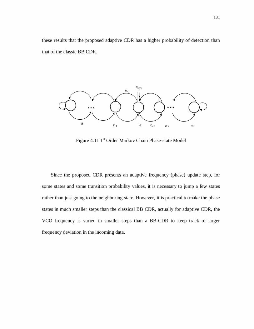
131
these results that the proposed adaptive CDR has a higher probability of detection than
that of the classic BB CDR.
Figure 4.11 1st Order Markov Chain Phase-state Model
Since the proposed CDR presents an adaptive frequency (phase) update step, for
some states and some transition probability values, it is necessary to jump a few states
rather than just going to the neighboring state. However, it is practical to make the phase
states in much smaller steps than the classical BB CDR, actually for adaptive CDR, the
VCO frequency is varied in smaller steps than a BB-CDR to keep track of larger
frequency deviation in the incoming data.
1−iφ iφ1+iφ
i,dnP
i,upP
i,holdP
0φLφ

132
Figure 4.12 The Probabilities of Up, Down and Hold Signal in Proposed CDR
Figure 4.13. Comparison of the Steady State Phase Probabilities for the Transition Probabilities
-0.1 -0.08 -0.06 -0.04 -0.02 0 0.02 0.04 0.06 0.08 0.10
0.1
0.2
0.3
0.4
0.5
0.6
0.7
0.8
0.9
1
p-up
p-dn
p-holdp-early
p-late
-0.1 -0.08 -0.06 -0.04 -0.02 0 0.02 0.04 0.06 0.08 0.10
0.01
0.02
0.03
0.04
0.05
0.06
0.07
0.08
0.09
0.1
classical CDR
adaptive CDR
Proposed CDR
Classic BB

133
The steady state probability of the possible phases of the recovered clock for
proposed CDR and conventional CDR are shown in Figure 4.13 and Figure 4.14, where
the X-axis is the possible CLK phase in UI.
The RMS jitter of the recovered clock can be estimated from the probability
distribution of the phases of the recovered clock. Thus the statistical analysis of the
steady state phase of the CDR will converge to the long-term jitter histogram of the
recovered clock. Notice in these results that the proposed CDR has better statistical
performance compared with the conventional BB-CDR architecture.
-0.02 -0.015 -0.01 -0.005 0 0.005 0.01 0.015 0.0210
-4
10-3
10-2
10-1
classical CDRadaptive CDR
Figure 4.14 The Logarithmic Plot of the Steady State Probabilities of Proposed and Classic BB CDR
Conventional CDR Proposed CDR

134
IV.5. Simulation Results
In the following experiment, a PRBS (pseudo-random bitstream) generator outputs
data pattern and the data is passed to a 5Gb/s CDR block which extracts the clock from
the incoming data. In this paper, only a bit error rate (BER) of 1e-4 is simulated for the
tradeoff of computing time.
The jitter measurement through sinusoidal jitter modulation in the input data is the
toughest in jitter tolerance test, and adopted in all of the Serial PHY standard such as
Gigabit Ethernet, SONET, PCI Express (PCIe) , SATA and Fiber Channel. For a typical
sinusoidal modulation jitter addition, we have:
( )02sin φπφ += tfA mSJSJ (4.17)
where fm and 0φ are sinusoidal modulation frequency and initial sinusoidal jitter phase,
respectively; ASJ is the sinusoidal phase modulation amplitude in rad/s, which can also
be measured in Unit intervals (UI). Since one UI corresponds to 2π, in our simulation,
the phase error jitter is measured in time units instead of rad/s, i.e, the recovered clock
phase has peak to peak deviation
bitSJpkpkSJpkpk TJ ,_,_ 2πφ = (4.18)
where Jpk-pk,SJ is the phase error jitter of the recovered clock in time unit; and Tbit is the
period of the input data pattern.

135
IV.5.1. Phase Tracking with 6MHz Sinusoidal Jitter Modulation (1st Order BB CDR)
All the experiments of 1st order BB CDR are performed with the data and clock
frequency deviation of 150ppm. For the 1st order BB CDR, the phase error tracking of
6MHz sinusoidal jitter is shown in Figure 4.15. The conventional BB CDR has an
equivalent bandwidth of 4.5MHz, while the adaptive has a steady state bandwidth of
2MHz. The phase error jitter5 for the adaptive CDR is 13.3ps peak to peak versus that of
22.4ps pk-to-pk in the conventional BB CDR.
Notice that in Figure 4.15,fδ , frequency difference between data and clock, is
150ppm. The waveform in (a) shows that the phase tracking of adaptive CDR is better
than of that in the classical BB CDR in (c).
IV.5.2. Phase Tracking with 2MHz Sinusoidal Jitter Modulation
In Figure 4.16, an initial frequency difference between data and clock is set to
150ppm for simulation. The traces from the top to the bottom are: (a) phase tracking of
conventional BB CDR; (b) phase tracking error of classical CDR; (c) phase tracking of
adaptive BB CDR; (d) phase error of 2MHZ SJ in adaptive BB CDR;(e) phase tracking
error comparison between adaptive BB CDR and conventional CDR. The conventional
BB CDR has an equivalent bandwidth of 4.5MHz, while the adaptive has a steady state
5 The phase error jitter is defined not as the rad/s, but the orginal phase error divided by 2, which is in unit interval, then it is multiplied by clock period which is measured in seconds.

136
bandwidth of 2MHz. The phase error jitter6 for the adaptive CDR is 11.7ps peak to peak
versus that of 20.4ps pk-to-pk in the conventional BB CDR.
IV.5.3. Phase Tracking with 6MHz Sinusoidal Jitter Modulation for a 2nd Order CDR
The following experiments for a 2nd order CDR were done with the data and clock
frequency deviation of 300ppm. Simulations for conventional second order BB-CDRs
configured with a steady state loop bandwidth of factors one (x1) and three times(x3) the
equivalent bandwidth of the adaptive CDR were carried out. Figure 4.17 shows the
phase error tracking for a second order CDR which is configured x1 and x3 of equivalent
bandwidth of an adaptive CDR. The phase error for the 1x conventional CDR is 19.8ps
pk-pk versus 12ps pk-pk of the x3 bandwidth configuration, while the adaptive CDR
presented a phase error of 11.3ps pk-pk. The adaptive CDR outperformed the x3
conventional CDR. Furthermore, as aforementioned, very large CDR bandwidth may
cause large phase errors when tracking low speed frequency jitter, making very difficult
the selection of the correct bandwidth unless the frequency of the sinusoidal jitter can be
accurately predicted. The adaptive CDR can achieve significant jitter optimization and
better jitter tolerance as tabulated in Table IV.2. For these results, 215-1 PRBS pattern
with frequency variation of 300ppm, and 0.15UI ISI distortion were used.
6 The phase error jitter is defined not as the rad/s, but the orginal phase error divided by 2, which is in unit interval, then it is multiplied by clock period which is measured in seconds.

137
Figure 4.15 Phase Tracking of 1st Order BB CDR with 6MHz Sinusoidal Jitter: (a) Phase Tracking of the Adaptive BB CDR, (b) Phase Tracking Error of the Adaptive BB CDR, (c) Phase Tracking of the Classical BB CDR, and (d) Phase Tracking Error of the Classical BB CDR
(a)
(b)
(c)
(d)

138
Large bandwidth in a conventional CDR does not necessarily track the sinusoidal jitter
optimally. The phase tracking performance is depicted in Figure 4.16 shows the
comparison for the conventional BB CDR with 12MHz bandwidth and the adaptive BB
CDR with only 2MHz bandwidth. Due to the large frequency step in the conventional
CDR, the phase tracking is similar to the one of a linear under-damped system response.
The peak to peak phase error jitter in the conventional CDR is 20.4ps versus 11.7ps in
the adaptive CDR.
Figure 4.16 Comparison of Phase Tracking between 1st Order Conventional and Adaptive BB CDR: (a) Phase Tracking of Conventional BB CDR, (b) Phase Tracking Error of Classical CDR, (c) Phase Tracking of Adaptive BB CDR, (d) Phase Error of 2MHZ SJ in Adaptive BB CDR and (e) Phase Tracking Error Comparison between Adaptive BB CDR and Conventional CDR
(a)
(b)
(c)
(d)
(e)

139
TABLE IV.2: SUMMARY OF SIMULATION RESULTS
Technology x1 BB CDR x3 BB CDR Adaptive CDR
Input data rate (Gb/s) 5 5 5
Equivalent BW 7MHz 9MHz 4MHz
Extracted sinusoidal pk-pk
jitter(ps) to track 6MHz SJ with
0.32UIpp
49.4 45.4 44.4
pk-pk phase error (ps) to track
6MHz SJ with 0.32UIpp 19.2 12 12
pk-pk phase error (ps) to track
3MHz SJ with 0.32UIpp 10.8 10.8 10.4
Figure 4.18 shows the simulation of the phase tracking of the adaptive and
conventional Bang-bang CDRs with input sinusoidal jitter amplitude of 0.34UIpp, at a
frequency of 6MHz. The steady state bandwidth of the conventional CDR (6MHz) is 3x
that of adaptive CDR (BW=2MHz). Theoretically, under steady state, the conventional
BB-CDR with BW=6MHz should track the sinusoidal jitter much better due to its
inherent larger bandwidth; however, simulation results show that the jitter tracking
performance of the adaptive CDR is better mainly because the bandwidth adjusting
mechanism. The adaptive CDR achieves a peak-to-peak phase error of 11.4ps while the
conventional CDR achieves 19.2ps.

140
For lower frequency sinusoidal jitter input both CDRs can track the sinusoidal jitter
since there is no slew rate limiting process in the tracing. Figure 4.18 confirms that both
architectures achieve similar phase error when tracking 3MHz sinusoidal jitter. In spite
of the advantage of the adaptive CDR, increasing the steady state equivalent bandwidth
of the conventional CDR, both topologies achieve good phase tracking performance. In
some cases it is unnecessary to perform the adaptive CDR but it is critical to consider the
following issues: i) as aforementioned, very large CDR bandwidth will cause large phase
error when tracking low speed frequency jitter; ii) it is not easy to predict which kind of
jitter is present at the input of the system; iii) some standards such as the typical Gigabit
Ethernet / SONET OC-192 require a 3dB bandwidth of only 120KHz, and a bandwidth
of several MHz will have to be either shaped by a transmitter with a narrower bandwidth,
or a digital FIFO and a bandwidth re-shaping PLL can be used to achieve such a
stringent and narrow bandwidth [11]. The incoming jitter is often unexpected; hence it is
difficult to define the optimal steady-state loop bandwidth. The beauty of the adaptive
CDR architecture is that, based on phase estimation, it adapts the loop bandwidth for the
best possible jitter tracking performance.
In Figure 4.18, the sinusoidal jitter (SJ) frequency is 6M Hz, the jitter amplitude is
0.32UIpk-pk; frequency difference between data and clock is 300ppm.From the
simulation results, the adaptive CDR has better phase tracking performance comparing
with the classical BB CDR design.

141
Figure 4.17 Phase Comparison of x1, x3 2nd Order , BB CDR and 2nd Order Adaptive BB CDR, Frequency Difference Is 300ppm: (a) Phase Tracking of Adaptive BB CDR, (b) Phase Tracking Error of Adaptive BB CDR, (c) Phase Tracking of Conventional BB CDR(x1 bandwidth), (d) Phase Tracking Error of Classical BB CDR(x1 BW), (e) Phase Tracking of Conventional BB CDR(x3 BW),(f) Phase Tracking Error of Conventional BB CDR(x3), (g) Comparison of CDR(x1BW) vs. BB CDR(x3), (h) Comparison of BBCDR(x3) vs. Adaptive BB CDR; and (i) The Comparison of CDR(x1),CDR(x3) and Adaptive CDR
(a)
(b)
(c)
(d)
(e)
(f)
(g)
(h)
(i)

142
Figure 4.18 Comparison of Phase Error Tracking of Adaptive Bang-bang CDR and Classical Bang-bang CDR: (a) Adaptive Phase Error Tracking, (b) Phase Error in Adaptive Bang-bang CDR, (c) Classic Bang-bang Phase Error Tracking(Slew Rate Limiting), (d) Classic BB CDR Phase Error Tracking, and (e) Phase Error Comparison
(a)
(b)
(c)
(d)
(e)

143
IV.6. Conclusions
A CDR with adaptive bang-bang control and hence adaptive bandwidth control has
been proposed. This architecture can be used in many applications such as PCIe, SATA
and Fiber channel for the chip-to-chip interface where jitter peaking requirements are
relaxed (3dB at a maximum). For stringent standards such as Gigabit Ethernet or
SONET OC-192, the adaptive BB-CDR outperforms the conventional BB-CDR due to
its phase dependent loop bandwidth, which leads to superior jitter tolerance performance.
Theoretical analysis, in good agreement with extensive simulations, supports the
foundations of the proposed architecture. This architecture can also be used in
DLL/phase interpolator based digital CDRs by varying the digital loop filter.

144
V. CONCLUSIONS
In this dissertation, two clock data recovery integrated circuits architecture used for
telecommunication or data communication systems have been discussed.
Firstly, a fully integrated 10-Gb/s CDR is implemented in a 0.18µm CMOS process.
The design uses half rate architecture due to the relative low ft (50GHz) of the CMOS
process used. By using a new loop filter and charge pump configuration, the chip
integrates all the components on-chip including the integration loop filter capacitor.
Improved charge pump architecture with source degeneration, VCO with amplitude
tuning and multiplexer scheme in double edged DFFs are the other techniques adopted to
enhance the chip performance. The CDR device can recover data with a BER less than
10-12 when the input eye closure is slightly above 0.5UIpp(Horizontal eye closure) and
the recovered clock with peak to peak jitter less than 0.1UIpp.The CDR also exceeds the
OC-192 jitter tolerance mask with high frequency jitter tolerance over 0.31UIpp. To the
best our knowledge, this reported implementation is the first fully integrated, PLL based
10Gb/s CDR in the literature.
Secondly, in a real world telecommunication or data communication application, the
jitter frequency is not known in advance, a CDR with too large or too low bandwidth
can not track the jitter in an optimal way, thus a CDR with adaptive bang-bang control
and hence adaptive bandwidth control has been proposed. This architecture can be used
in many applications such as PCIe, SATA and Fiber channel for the chip-to-chip
interface where jitter peaking requirements are relaxed (3dB at a maximum). For

145
stringent standard such as Gigabit Ethernet or SONET OC-192, the adaptive BB-CDR
outperforms the conventional BB-CDR due to its phase dependent loop bandwidth,
which leads to a superior jitter tolerance performance. Theoretical analysis, in good
agreement with extensive simulations, supports the foundations of the proposed
architecture. This architecture can also be used in DLL/phase interpolator based digital
CDRs by configuring the digital loop filter easily.

146
REFERENCES
[1] M. J. Reizenman, “Optical nets for even heavier traffic,” IEEE Spectrum, pp.44-45,
Jan. 2001; [Online].Available: http://www.digitaltvdesignline.com/news/199904547,
EE Times, Jun. 2007.
[2] D. Wolaver, Phase-Locked Loop Circuit Design, Englewood Cliffs, NJ: Prentice
Hall Inc, 1991.
[3] “Synchronous optical network (SONET) transport systems: common generic
criteria,” Piscataway, NJ: Telecordia Technologies (Bellcore Standard), GR-253-
CORE, no. 3, 2000.
[4] L. Henrickson, D. Shen, U. Nellore, A. Ellis, O. Joong, H. Wang; G. Capriglione, A.
Atesoglu, A.Yang, P. Wu, S. Quadri, D. Crosbie, “Low-power fully integrated 10-
Gb/s SONET/SDH transceiver in 0.13-µm CMOS,” IEEE J. Solid State Circuits, vol.
38, no. 10, pp. 1595-1601, Oct. 2003.
[5] H. Cong, S. Logan, M. Loinaz, K. O’Brien, E. Perry, G. Polhemus, J. Scoggins, K.
Snowdon, and M. G. Ward, “A 10-Gb/s 16:1 multiplexer and 10-GHz clock
synthesizer in 0.25-µm SiGe BiCMOS,” IEEE J. Solid-State Circuits, vol. 36, no. 12,
pp.1946-1953, Dec. 2001.
[6] Y. Greshishchev, P. Schvan, J. Showell, M. Xu, J. Ojha, and J. Rogers, “A fully
integrated SiGe receiver IC for 10-Gb/s data rate,” IEEE J. Solid-State Circuits, vol.
35, no.12, pp. 1949-1957, Dec. 2000.

147
[7] M. Meghelli, B. Parker, H. Ainspan, and M. Soyuer, “SiGe BiCMOS 3.3 V clock
and data recovery circuits for 10Gb/s serial transmission systems,” in IEEE Int.
Solid-State Circuits Conf. (ISSCC) Dig. Tech. Papers., Feb. 2000, pp. 56-57.
[8] J. Hauenschild, C. Dorschky, T. vonMohrenfels, and R. Seitz, “A plastic packaged
10 Gb/s BiCMOS clock and data recovering 1:4-demultiplexer with external
VCO,”IEEE J. Solid-State Circuits, vol. 31, no. 12, pp. 2056 – 2059, Dec. 1996.
[9] R.C. Walker, R. C., K. Hsieh, T. A. Knotts, and C. Yen, “A 10Gb/s Si-bipolar
TX/RX chipset for computer data transmission,” in IEEE Int. Solid-State Circuits
Conf. (ISSCC) Dig. Tech. Papers, Feb. 1998, pp. 302-303.
[10] J. Savoj and B. Razavi, “A 10-Gb/s CMOS clock and data recovery circuit with
frequency detection,” in IEEE Int. Solid-State Circuits Conf. (ISSCC) Dig. Tech.
Papers., Feb. 2001, pp. 78-79.
[11] J. Cao, A. Momtaz, K. Vakilian, M. Green, D. Chung, K. Jen; M. Caresosa, B. Tan,
I. Fujimori, and A. Hairapetian, “OC-192 receiver in standard 0.18µm CMOS,” in
IEEE Int. Solid-State Circuits Conf. (ISSCC) Dig. Tech. Papers., Feb. 2002, pp. 250-
251.
[12] J.E. Rogers and J.R. Long, “A 10Gb/s CDR/Demux with LC delay line VCO in
0.18µm CMOS,” in IEEE Int. Solid-State Circuits Conf. (ISSCC) Dig. Tech. Papers.,
Feb. 2002, pp. 254-255.
[13] S. Sidiropoulos, N. Acharya, P. Chau; J. Dao, A. Feldman, H. Liaw, M. Loinaz, R.
Narayanaswami, C. Portmann, S. Rabii, A. Salleh, S. Sheth, L. Thon, K. Vleugels, P.
Yue, and D. Stark, “An 800 mW 10 Gb Ethernet transceiver in 0.13µm CMOS,” in

148
IEEE Int. Solid-State Circuits Conf. (ISSCC) Dig. Tech. Papers., Feb. 2004, pp. 168-
169.
[14] T.O. Anderson, W.J. Hurd, and W.C. Lindsey, “Transition tracking bit
synchronization system,” US patent 626298, Dec. 1971.
[15] A. Buchwald and K. Martin, Integrated Fiber-Optic Receivers, Norwell, MA:
Kluwer Academic Publishers, 1995.
[16] C. Hogge, “A self correcting clock recovery circuit,” IEEE J. Lightwave
Technology, vol. 3, no. 6, pp. 1312-1314, Dec. 1985.
[17] T.H. Lee and J.F. Bulzacchelli, “A 155-MHz clock recovery delay- and phase-
locked loop, ” IEEE J. Solid-State Circuits, vol. 27 no. 12 , pp. 1736 -1746, Dec.
1992.
[18] T. H. Lee, The Design of CMOS Radio Frequency Integrated Circuits, Cambridge,
UK: Cambridge University Press, 1998.
[19] B. Lai and R.C. Walker,” A monolithic 622Mb/s clock extraction data retiming
circuit,” in IEEE Int. Solid-State Circuits Conf. (ISSCC) Dig. Tech. Papers., Feb.
1991, pp.144 –306.
[20] Y.M. Greshishchev and P. Schvan, “SiGe clock and data recovery IC with linear-
type PLL for 10-Gb/s SONET application,” IEEE J. Solid-State Circuits, vol. 35
no.9 , pp. 1353 -1359, Sep. 2000.
[21] B. Razavi, Design of Integrated Circuits for Optical Communications, New York,
NY: McGraw-Hill Publishing, 1st ed., 2002.

149
[22] J. Lee, K. Kundert, and B. Razavi, “Analysis and modeling of bang-bang clock and
data recovery circuits,” IEEE J. Solid-State Circuits, vol. 39, no. 9, pp. 1571-1580,
Sep. 2004.
[23] A. Pottbaker and U. Langmann, “An 8 GHz silicon bipolar clock-recovery and data-
regenerator IC,” IEEE J. Solid-State Circuits, vol. 29, no.12, pp. 1572-1576, Dec.
1994.
[24] W. Rhee, “Design of high-performance CMOS charge pumps in phase-locked
loops,” in Proc. IEEE Int. Symp. Circuits and Systems (ISCAS), 1999, pp.545-548.
[25] A. Valero-Lopez, “Design of frequency synthesizers for short range wireless
transceivers,” Ph.D Dissertation, Dept. Elect. Eng., Texas A&M Univ, College
Station, TX, 2004.
[26] M. Johnson and E. Hudson, “A variable delay line PLL for CPU-coprocessor
synchronization,” IEEE J. Solid-state Circuits, vol. 23, pp. 1218-1223, Oct. 1988.
[27] I. A. Young, J. K. Greason, and K. L. Wong, “A PLL clock generator with 5 to
110MHz of lock range for microprocessors,” IEEE J. Solid-State Circuits, vol. 27,
no. 11, pp. 1599-1607, Nov. 1992.
[28] L. Lin, “Design techniques of high performance integrated frequency synthesizer for
Multi-standard wireless communication applications,” Ph.D dissertation, Dept. Elect.
Eng., Univ California, Berkeley, CA, 2000.
[29] I. Novof, J. Austion, R.Kekar, D.Strayer and S. Wyatt, “Fully integrated CMOS
phase-locked loop with 15 to 240MHz locking range and ±50 ps jitter,” IEEE J.
Solid-State Circuits, vol. 30, no. 11, pp. 1599-1607, Nov. 1995.

150
[30] H.Werker, S. Mechnig, C. Holuigue, C. Ebner, G. Mitteregger, E. Romani, F. Roger,
T. Blon, M. Moyal, M. Vena, A. Melodia, J. Fisher, J.G. de Mercey, and H. Geib, “A
10Gb/s SONET-compliant CMOS transceiver with low cross-talk and intrinsic
jitter,” in IEEE Int. Solid-State Circuits Conf.(ISSCC) Dig. Tech. Papers., Feb. 2004,
pp.172-173.
[31] A. Hajimiri and T. H. Lee, “Design issues in CMOS differential LC oscillators,”
IEEE J. Solid-State Circuits, vol. 34, no. 5, pp. 717-724, May 1999.
[32] J. Jael and A. Abidi, “Physical processes of phase noise in differential LC
oscillators,” in Proc. IEEE Custom Integrated Circuits Conf.(CICC), May 2000, pp.
569-572.
[33] E. Hegazi, H. Sjoland, and A. Abidi, “A filtering technique to lower LC oscillator
phase noise,” IEEE J. Solid-State Circuits, vol. 36, no.12, pp.1921-1930, Dec. 2001.
[34] H. Darabi and A. Abidi, “Noise in CMOS mixers: a simple physical model,” IEEE J.
Solid-State Circuits, vol. 35, no.1, pp. 15-25, Jan. 2000.
[35] A. Rofougaran, G. Chang, J. Rael, M. Rofougaran, S. Khorram, M. Ku, E. Roth, A.
Abidi, H. Samueli, “A 900MHz CMOS LC-oscillator with quadrature outputs,” in
IEEE Int. Solid-State Circuits Conf. (ISSCC) Dig. Tech. Papers, Feb. 1996, pp. 391-
393.
[36] T. P. Liu, “1.5 V 10-12.5 GHz integrated CMOS oscillators,” in IEEE Int. Solid-
State Circuits Conf. (ISSCC) Dig. Tech. Papers, Feb. 1999, pp. 404-405.

151
[37] C. Lo and H. Luong, “2-V 900-MHz Quadrature coupled LC oscillators with
improved amplitude and phase matching,” in Proc. IEEE Symp. Circuits and Systems
(ISCAS), 1999, pp. 585-588.
[38] M. Meghelli, A.V Rylyakov, S.J Zier, M. Sorna, and D. Friedman, “A 0.18µm SiGe
BiCMOS receiver and transmitter chipset for SONET OC-768 transmission
systems,” IEEE J. Solid-State Circuits, vol. 38, no. 12, pp. 2147-2154, Dec. 2003.
[39] J. Craninckx and M. Steyaert, “A fully integrated CMOS DCS-1800 frequency
synthesizer,” IEEE J. Solid-State Circuits, vol. 33, no. 12, pp. 2054-2065, Dec. 1998.
[40] A. Maxim, B. Scott, E. Schneider, M. Hagge, S. Chacko, and D. Stiurca, “ Low-
jitter 125-1250-MHz process-independent and ripple-poleless 0.18-µm CMOS PLL
based on a sample-reset loop filter,” IEEE J. Solid-State Circuits, vol. 36, no.11, Nov.
2001.
[41] R.C. Walker, C. Stout, J. Wu, B. Lai, C. Yen, T. Hornak, P. Petruno, “A two-chip
1.5-GBd serial link interface,” IEEE J. Solid-State Circuits, vol. 27, no. 12, pp.
1805-1811, Dec. 1992.
[42] E. Youssoufian and T. Sowlat, "Method and apparatus for loop filter size
reduction," US Patent Application # 20060267644, Nov. 2006.
[43] E. Sackinger and W.C. Fischer, “A 3-GHz 32 dB CMOS limiting amplifier for
SONET OC-48 receivers,” IEEE J. Solid State Circuits, vol. 35, no.12, pp.1884-
1888, Dec. 2000.
152
[44] E. M. Cherry, D. E. Hooper,and M. E. Gradulates, “The design of wide-band
transistor feedback amplifier,” Proceedings IEE, vol. 110, no. 2, pp. 375-389, Feb.
1963.
[45] A. Hajimiri, S. Limotyrakis, and T.H. Lee, “Jitter and phase noise in ring
oscillators,” IEEE J. Solid-State Circuits, vol. 34, no. 6, pp. 790-804, Jun. 1999.
[46] J. Li and J. Silva-Martinez, “A multi-gigabit/s clock data recovery architecture using
an adaptive bang-bang control strategy,” submitted to IEEE Trans. Circuits Syst. I:
Fundamental Theory and Applications, to appear.
[47] F. Herzel and B. Razavi, “A study of oscillator jitter due to supply and substrate
noise,” IEEE Trans. Circuits and Systems-II: Analog and Digital Signal Processing,
vol. 46, no. 1, pp. 56-62, Jan. 1999.
[48] J. Silva-Martinez and M. Steyaert, and W. Sansen, High-Performance CMOS
Continuous-time Filters, Dordrecht, The Netherlands: Springer, 1993.
[49] “Fiber channel-methodologies for jitter and signal quality specification (MJSQ),”
Washington DC: International Committee for Information Technology Standards
(INCITS), Tech. Rev. 13.2, May 2004.
[50] D. Pozar, Microwave Engineering, New York, NY: John Wiley & Sons Inc, 2005.
[51] H. Takauchi, H. Tamura, S. Matsubara, M. Kibune, Y. Doi, T. Chiba, H. Anbutsu,
H. Yamaguchi, T. Mori, M. Takatsu, K. Gotoh, T. Sakai, and T. Yamamura, “A
CMOS multichannel 10-Gb/s transceiver,” IEEE J. Solid-State Circuits, vol. 38,
no.12 , pp. 2094-2100, Dec. 2003.

153
[52] J. Li and J. Silva-Martinez, “A fully on-chip 10Gb/s CMOS CDR,” Accepted, IEEE
Trans. Circuits Syst. I: Fundamental Theory and Applications, to be appearing.
[53] R. C. Walker, “Designing bang-bang PLLs for clock and data recovery in serial data
transmission systems,” in Phase-Locking in High-Performance Systems-From
Devices to Architecture, B. Razavi, Ed., New York, NY: IEEE Press, 2003.
[54] C. Kromer, G. Sialm, C. Menolfi, M. Schmatz, F. Ellinger and H. Jackel, “A 25-
Gb/s CDR in 90-nm CMOS for high-density interconnects,” IEEE J. Solid State
Circuits, vol.41, no. 2, pp. 2921 – 2929, Dec. 2006.
[55] H. Lee, A. Bansal, Y. Frans, J. Zerbe, S. Sidiropoulos, and M. Horowitz,
“Improving CDR performance via estimation,” in IEEE Int. Solid-State Circuits
Conf.(ISSCC) Dig. Tech. Papers, pp.1296-1303, Feb.,2006.
[56] N. S. Jayant, “Digital coding of speech waveforms: PCM, DPCM, and DM
quantizers,” Proc. IEEE, vol. 62, no. 5, pp.611-632, May 1974.
[57] R. Steele, Delta Modulation Systems, New York, NY: John Wiley & Sons, 1975.
[58] A. Papoulis, Probability, Random Variables, and Stochastic Processes, New York,
NY: McGraw Hill, 1984.
[59] V. Stojanovic and M. Horowitz, “Modeling and analysis of high-speed links,” in
Proc. IEEE Custom Integrated Circuits Conf.(CICC), Sep. 2003, pp. 589-594.
[60] M. Meghelli, B. Parker, H. Ainspan, and M. Soyuer, “SiGe BiCMOS 3.3 V clock
and data recovery circuits for 10Gb/s serial transmission systems,” IEEE J. Solid-
State Circuits, vol. 35, no. 12, pp.1992-1995, Dec. 2000.

154
[61] J. Cao, A. Momtaz, K. Vakilian, D. Chung, K. Jen; M. Caresosa, X. Wang, W. Tan,
Y. Cai; I. Fujimori, A. Hairapetian, “OC-192 transmitter and receiver in standard
0.18µm CMOS,” IEEE J. Solid-State Circuits, vol. 37,no.12, pp. 250-251, Feb. 2002.
[62] N. Da Dalt, “A design-oriented study of the nonlinear dynamics of digital bang-
bang PLLs,” IEEE Trans. Circuits Syst. I: Fundamental Theory and Applications,
vol. 52, no.1, pp. 21-31, Jan. 2005.
[63] A. Gelb and W. V. Velde, Multiple-Input Describing Functions and Nonlinear
System Design, New York, NY: McGraw-Hill, 1968.

155
APPENDIX A
LOOP DYNAMICS OF THE CDR LOOP
In this dissertation, the CDR is based on charge pump PLL configuration. The CDR
diagram is represented in Figure A.1, the Kpd is the gain of the combined phase detector
and charge pump in Figure 2.1. F(s) is the loop filter, and Kvco/S is the representation of
the VCO used in the CDR loop.
Figure A.1 Phase Diagram of a Typical CDR loop
Now neglect the parallel capacitor C2 in Figure 2.1, the loop filter can be represented in
the laplace s-domain as
( ) ( )s
CRsR
sCRsF 11
11
1
11 +=+= (A.1)
The phase(jitter) transfer function from φ in to φ out can be obtained as [2]
22
2
2
2
)(
)()(
nn
nn
in
out
ss
s
s
ssH
ωξωωζω
φφ
+++
== (A.2)
where ( ) 1112122 ,,,5.0 −==== CRRKKKKK vcopdn ωωωωξ .The jitter
peaking can be derived by find the maximum of the magnitude of the H(s=jω), namely,
+ Kpd F(s) sKvco
inφoutφ
156
by solving ( )( ) 02 =ω
ωjH
d
d, the peaking value is solved as
( )[ ]Kwhen
K
KwhereJP
1.01
22221
22
2
212122
<+≅
=++−−=−
ωωωαααααα
(A.3)
The jitter tolerance describes how much input jitter a CDR must tolerate without
increasing the bit error rate, and it is determined by [21]
∞→+
≅
++=
−=
sass
s
s
ss
sHsJTOL
n
nn
ξω
ωξω
2
2
1
2
2
1
)(1
5.0)(
2
22
(A.4)
An example of jitter transfer curve is shown in Figure A.2, the peaking increases with
the increase of ω 2/K. The jitter tolerance curve is shown in Figure A.3.

157
Figure A.2 Jitter Transfer curve for a CDR with a Bandwidth of 6MHz
Figure A.3 Jitter Tolerance Curve for a CDR with a Jitter Transfer Curve of Figure A.2
105
106
107
108
109
-20
-15
-10
-5
0
Frequency (Hz)
Jitt
er T
rans
fer
w2/K=0.02w2/K=0.04
w2/K=0.06
w2/K=0.1
w2/K=0.3Mask

158
APPENDIX B
COARSE FREQUENCY TUNING CIRCUIT IN THE CDR
The coarse frequency tuning circuit is composed of the output range detector of the
loop filter output and SAR control logic, as shown in Figure B.1. In the output range
detector of the loop filter, the VCO tuning voltage Vc is compared with two reference
voltages, Vref+ and Vref-. The outputs of the two comparators cmp_H and cmp_L
represent whether the loop filter voltage is out of range or not [21]. The operation
principle is shown in Table B.1. Basically, when Vc > Vref+, which means the VCO is not
slow enough, thus more variable capacitance should be placed in the LC tank; when Vc <
Vref-, the VCO needs to speed up such that Vc doesn’t reduce further.
The SAR control logic works as follows, after the start pulse is asserted low, the
shift registers output the sequence of pulses, q<5:0>. Shown in Figure B.2, the SAR
output q<5> first outputs a ‘1’, and the capacitor array control bit C<5> is also ‘1’; when
the range detector output cmp is ‘1’; then q<4> and q<3> output ‘1’, and C<4> and
C<3> are both set to ‘1’s as the cmp still keeps high; then when the range detector
outputs ‘0’, thus C<2> is set to ‘0’, etc. Besides the automatic SAR control, the capacitor
bank can also be set manually by pull p<5:0> control bits to low to add more capacitor
arrays.

159
Figure B.1 Coarse Frequency Tuning Circuit
TABLE B.1 Principle of the voltage range detector of loop filter output
Cmp_H Cmp_L
Operation
0 0
Vc> Vref+, Vc>Vref-; Increase capacitance
0 1
Vc>Vref+, Vc<Vref-; Reset the range detector
1 0
Vref-<Vc<Vref; No operation
1 1
Vc<Vref+, Vc<Vref-; Reduce the capacitance
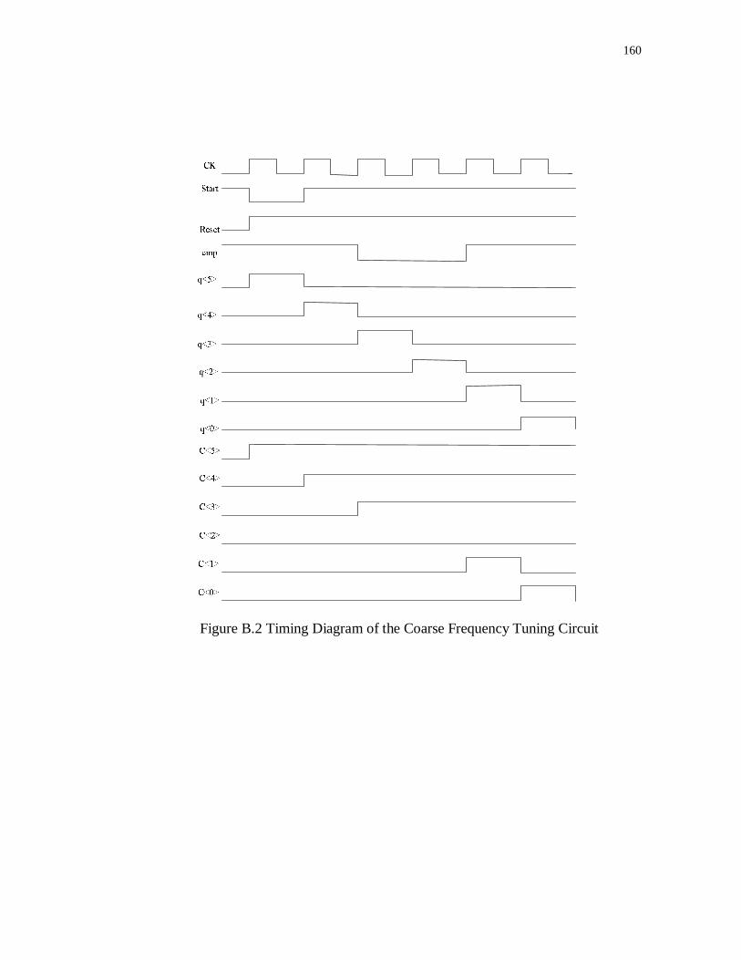
160
Figure B.2 Timing Diagram of the Coarse Frequency Tuning Circuit

161
APPENDIX C
DETERMINATION OF THE BANDWIDTH OF THE BB-CDR
Unlike the linear systems, which can be studied through classical Laplace/Fourier
transform in frequency domain, the binary phase detector based clock recovery
architecture is a nonlinear system and the frequency response functions of nonlinear
elements cannot be defined directly [53],[61],[62]. The binary CDR phase error
converges to a limit cycle in a phase plane instead of settling to a relatively constant
value as in the case of linear CDRs. Thus, it is mandatory to perform complete transient
simulations. However, it is not very appropriate in the first stage of the design of a
nonlinear system because one must wonder whether enough initial condition and input
combinations are covered in the resultant system response. Although not accurate, the
Describe Function (DF) gives a quasi-linear approximation representation of the
nonlinearities by minimizing the mean-squared approximation error with sinusoidal or
random inputs applied to the nonlinear element [63]. A convenient way to derive the DF
is exciting the nonlinear system with a sinusoidal signal; the output of the non-linear
device generally consists of the harmonics of the input sinusoidal signal[63]. Discarding
all other frequency components except the one with the same frequency as the input, the
ratio transfer function between that output component and the input signal defines the
DF. As an example, the ideal comparator has the form Vout=D*sgn(Vin); when excited by
a sinusoidal signal ( )tAVin ωsin= ,its frequency equivalent is given by

162
( )∑∞=1
,sin4
n
tnDVout
ωπ
where n is an odd number. Keeping only the fundamental tone,
and dividing the output component by the input signal, we get DF = 4D/πA, which is
inverse proportional to the amplitude of the input tone A. Thus it is easy to understand
why the jitter transfer of a binary PD based CDR is inverse proportional to the input
jitter amplitude. Even though the DF method is only an approximation, it is a good tool
to predict limit cycles in nonlinear systems. However, due to its nonlinear nature, it is
not surprising that the results are somewhat not accurate and further system simulations
are needed to verify system functionality.
Figure C.1. Block Diagram of a Binary PD Based CDR
The limit cycle of the binary PD based clock recovery can be determined by
analyzing its close-loop transfer function, namely the following equation:
dτ

163
( ) ( ) 01 =+ ωjLAN (C.1)
where N(A) is the describe function of the nonlinear binary phase detector whose
characteristic is drawn in Figure C.1 ; A is the potential limit cycle amplitude and L(jω)
is the Fourier transform of the linear part of the system; KVCO is the gain of the VCO; Icp
is the charge pump current, and τz =RZCZ is the time constant associated with the loop
filter. Td is the systematic loop delay. L(ω) can be derived from the linear part of the
loop, see Figure C.1, as follows
( ) ( )dd szs
cpVCOz
z es
sKeIK
Cs
ssL ττ ττ −− +=+=
22
11 (C.2)
where zCPVCO CIKK = . The describing function for the non-linear phase detector can
be mathematically model as
( ) =A
fD
ANδ
δ (C.3)
where A is the amplitude of the input sinusoidal signal, ( )tAtVin ωsin)( = , and f is the
following function [63]

164 −+= −2
1 1sin2
AAAAf
δδδπ
δ (C.4)
The loop bandwidth limitation to guarantee loop stability can be obtained
combining equations (C.1-C.3); the resulting expression is
( ) =+ −
ADf
ejK
dLCj
LC
zLC
δδ
ωτω τω2
1 (C.5)
In this expression LCω is the frequency at which (C.1) is satisfied. To satisfy (C.5),
two conditions are required; for the magnitude we have
( )ADf
KzLC
LCδδτω
ω=+122
2 (C.6)
Therefore, the potential limit cycle amplitude can be obtained as +−=
121 22zDKf
A
LCLC τδ
δ
ωω (C.7)
where f-1(x) is the inverse function of f(x); see expression (C.4). A second condition is
associated with the phase of the left-hand side term of expression (C.5); thus, the
following second condition arises

165
( ) ...,2,1,0;2tan 1 ±±==−− nndLCzLC πτωτω (C.8)
From (C.8), and assuming that the tan-1(ωLCτZ) ≅ ωLCτZ a simplified expression for
the potential limit cycle frequency can be obtained
dzLC
n
ττπω
−≅ 2
(C.9)
It is worth mentioning that for a binary phase detector clock recovery system which
uses first order loop filter, and assuming that τd=0, the system will not show any limit
cycle dynamics.
In a typical binary CDR system the systematic delay τd, due to phase detector delay
and divider delay (if any), contributes to the limit cycle dynamics. Thus it is necessary to
adopt the phase detector with less delay or delay immune phase detector to improve the
system performance.

166
VITA
Jinghua Li was born in Shandong Province, P. R. China in 1973. He received his
B.S. degree from Harbin Engineering University, Harbin, China, in 1994, and the M.S.
degree from the Shanghai Jiaotong University, Shanghai, China in 1997, both in
electrical engineering. He was a research/teaching assistant in the Department of
Electrical Engineering, Texas A&M University in the Analog and Mixed-Signal Center
since the Fall of 2000. Since the summer of 2002, he worked toward the Ph.D. degree
under the advice of Dr. Jose Silva-Martinez and received his degree in December 2008.
He worked as an internship design engineer with Optical Transport Department,
Agere Systems(now LSI Logic), Allentown, PA from June to December 2002. From
June 1998 until June 2000, he was a Member of technical staff at Bell Labs(China),
Lucent Technologies, working on single-chip HDTV design using 0.25um CMOS
technology in Murray Hill, NJ, USA and Shanghai, China, respectively. His research
interests include analog and mixed-signal circuit design for high speed serial link design.
He can be reached at his email address of [email protected], or through Dr. Jose Silva-
Martinez, 318D, Wisenbaker Engineering Research Center, Analog and Mixed Signal
Center, Department of Electrical Engineering, Texas A&M University, College Station,
Texas 77843-3128, USA.