A-5.4-mW-180-cm-Transmission-Distance-2.5-Mbs-Advanced-Techniques-Based-Novel-Intrabody-Communication-Receiver-Analog-Front-End.pdf...
13
This article has been accepted for inclusion in a future issue of this journal. Content is final as presented, with the exception of pagination. IEEE TRANSACTIONS ON VERY LARGE SCALE INTEGRATION (VLSI) SYSTEMS 1 A 5.4-mW 180-cm Transmission Distance 2.5-Mb/s Advanced Techniques-Based Novel Intrabody Communication Receiver Analog Front End Hao Wang, Student Member, IEEE, Xian Tang, Member, IEEE, Chiu Sing Choy, Ka Nang Leung, Senior Member, IEEE , and Kong Pang Pun, Senior Member, IEEE Abstract—This paper presents a low power, long-transmission distance, high data rate intrabody communication (IBC) analog receiver front end (RFE). First, to optimize the transmission performance, conventional transmission line analysis scheme is creatively adopted to the IBC design to characterize the body channel. Second, switched-capacitor filters based on sampling rate boosting technique are adopted for higher accuracy and lower power consumption. Third, a novel RFE topology is proposed to further enhance the IBC performance. The new RFE is designed and fabricated in a standard 180-nm CMOS process. Measurement results show that the RFE can successfully transmit data spanning the whole human body, around 180 cm, which is one of the longest transmission distances reported in related literatures. Furthermore, it reaches a maximum data rate of 2.5 Mb/s with a bit error rate less than 1e-7 and consumes 5.4 mW from a 1.8 V supply. The proposed RFE compares favorably to similar reported works. Index Terms— Bit error rate (BER), intrabody communica- tion (IBC), matching network, receiver front end (RFE), sampling rate boosting, switched-capacitor (SC) filter, transmission distance, transmission line (TL). I. I NTRODUCTION N OWADAYS, with the invention and proliferation of smart wearable electronic devices like cell phones, smart watches and glasses, bio-medical sensors, and so on, off-air communication techniques, such as capacitive coupling used in these devices, have gained a lot of attention in the research community. As a major branch of body area network, intrabody communication (IBC) uses the human body as a communication medium to implement data transmission between various wearable devices, as shown in Fig. 1. Comparing with other conventional wireless techniques, IBC offers the advantages of low radiation, low power Manuscript received August 7, 2014; revised October 31, 2014; accepted November 23, 2014. H. Wang, C. S. Choy, K. N. Leung, and K. P. Pun are with the Department of Electronic Engineering, the Chinese University of Hong Kong, Hong Kong (e-mail: [email protected]; [email protected]; [email protected]; [email protected]). X. Tang was with the Department of Electronic Engineering, the Chinese University of Hong Kong. He is now with the Graduate School at Shenzhen, Tsinghua University, Shenzhen 518055, China (e-mail: [email protected]). Color versions of one or more of the figures in this paper are available online at http://ieeexplore.ieee.org. Digital Object Identifier 10.1109/TVLSI.2014.2379443 Fig. 1. Devices’ communication network based on IBC. consumption, high data rate, widebandwidth, small area, and privacy. Anticipating the significant role that IBC will play in the near future, researchers have spent much effort on the modeling of human body channel [1], [2]. However, existing models are largely based on electromagnetic field theory and are not readily applicable to IBC physical layer design. This has a serious impact on realizing IBC to its full commercial potential. Furthermore, achieving high-transmission speed (>1 Mb/s) across body tissues acting as parasitic capacitors and resistors is very difficult. Ensuring good transmission performance at high data rate and over long distance is a big challenge. Moreover, in conventional IBC RFE design, RC filter and hysteretic comparator are often used in signal recovery and signal level threshold decision. They suffer from large device mismatches and high power consumption, further limiting the progress of IBC development. To tackle the above problems, the following techniques based on electric-field IBC theory [2] and wideband signaling IBC scheme [3], are proposed in this paper: first, matching network is explored to optimize the body communication channel parameters. An IBC transmission channel is formed by coupling electric field between electrodes and body. With increasing signal frequency, the body communication channel can be modeled as a transmission line (TL). As a result, impedance matching network, from the transmitter (TX) 1063-8210 © 2014 IEEE. Personal use is permitted, but republication/redistribution requires IEEE permission. See http://www.ieee.org/publications_standards/publications/rights/index.html for more information.
-
Upload
nguyentankiet18 -
Category
Documents
-
view
231 -
download
4
Transcript of A-5.4-mW-180-cm-Transmission-Distance-2.5-Mbs-Advanced-Techniques-Based-Novel-Intrabody-Communication-Receiver-Analog-Front-End.pdf...

This article has been accepted for inclusion in a future issue of this journal. Content is final as presented, with the exception of pagination.
IEEE TRANSACTIONS ON VERY LARGE SCALE INTEGRATION (VLSI) SYSTEMS 1
A 5.4-mW 180-cm Transmission Distance 2.5-Mb/sAdvanced Techniques-Based Novel IntrabodyCommunication Receiver Analog Front End
Hao Wang, Student Member, IEEE, Xian Tang, Member, IEEE, Chiu Sing Choy,Ka Nang Leung, Senior Member, IEEE, and Kong Pang Pun, Senior Member, IEEE
Abstract— This paper presents a low power, long-transmissiondistance, high data rate intrabody communication (IBC) analogreceiver front end (RFE). First, to optimize the transmissionperformance, conventional transmission line analysis scheme iscreatively adopted to the IBC design to characterize the bodychannel. Second, switched-capacitor filters based on samplingrate boosting technique are adopted for higher accuracy andlower power consumption. Third, a novel RFE topology isproposed to further enhance the IBC performance. The new RFEis designed and fabricated in a standard 180-nm CMOS process.Measurement results show that the RFE can successfully transmitdata spanning the whole human body, around 180 cm, whichis one of the longest transmission distances reported in relatedliteratures. Furthermore, it reaches a maximum data rate of2.5 Mb/s with a bit error rate less than 1e-7 and consumes 5.4 mWfrom a 1.8 V supply. The proposed RFE compares favorably tosimilar reported works.
Index Terms— Bit error rate (BER), intrabody communica-tion (IBC), matching network, receiver front end (RFE),sampling rate boosting, switched-capacitor (SC) filter,transmission distance, transmission line (TL).
I. INTRODUCTION
NOWADAYS, with the invention and proliferation ofsmart wearable electronic devices like cell phones,
smart watches and glasses, bio-medical sensors, and so on,off-air communication techniques, such as capacitive couplingused in these devices, have gained a lot of attention in theresearch community. As a major branch of body area network,intrabody communication (IBC) uses the human body asa communication medium to implement data transmissionbetween various wearable devices, as shown in Fig. 1.Comparing with other conventional wireless techniques,IBC offers the advantages of low radiation, low power
Manuscript received August 7, 2014; revised October 31, 2014; acceptedNovember 23, 2014.
H. Wang, C. S. Choy, K. N. Leung, and K. P. Pun are with theDepartment of Electronic Engineering, the Chinese University of Hong Kong,Hong Kong (e-mail: [email protected]; [email protected];[email protected]; [email protected]).
X. Tang was with the Department of Electronic Engineering, the ChineseUniversity of Hong Kong. He is now with the Graduate Schoolat Shenzhen, Tsinghua University, Shenzhen 518055, China (e-mail:[email protected]).
Color versions of one or more of the figures in this paper are availableonline at http://ieeexplore.ieee.org.
Digital Object Identifier 10.1109/TVLSI.2014.2379443
Fig. 1. Devices’ communication network based on IBC.
consumption, high data rate, widebandwidth, small area,and privacy. Anticipating the significant role that IBC will playin the near future, researchers have spent much effort on themodeling of human body channel [1], [2]. However, existingmodels are largely based on electromagnetic field theory andare not readily applicable to IBC physical layer design. Thishas a serious impact on realizing IBC to its full commercialpotential. Furthermore, achieving high-transmission speed(>1 Mb/s) across body tissues acting as parasitic capacitorsand resistors is very difficult. Ensuring good transmissionperformance at high data rate and over long distance is abig challenge. Moreover, in conventional IBC RFE design,RC filter and hysteretic comparator are often used in signalrecovery and signal level threshold decision. They sufferfrom large device mismatches and high power consumption,further limiting the progress of IBC development.
To tackle the above problems, the following techniquesbased on electric-field IBC theory [2] and wideband signalingIBC scheme [3], are proposed in this paper: first, matchingnetwork is explored to optimize the body communicationchannel parameters. An IBC transmission channel is formedby coupling electric field between electrodes and body. Withincreasing signal frequency, the body communication channelcan be modeled as a transmission line (TL). As a result,impedance matching network, from the transmitter (TX)
1063-8210 © 2014 IEEE. Personal use is permitted, but republication/redistribution requires IEEE permission.See http://www.ieee.org/publications_standards/publications/rights/index.html for more information.
This article has been accepted for inclusion in a future issue of this journal. Content is final as presented, with the exception of pagination.
2 IEEE TRANSACTIONS ON VERY LARGE SCALE INTEGRATION (VLSI) SYSTEMS
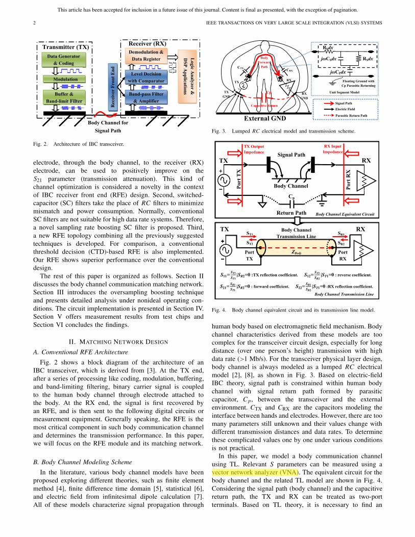
Fig. 2. Architecture of IBC transceiver.
electrode, through the body channel, to the receiver (RX)electrode, can be used to positively improve on theS21 parameter (transmission attenuation). This kind ofchannel optimization is considered a novelty in the contextof IBC receiver front end (RFE) design. Second, switched-capacitor (SC) filters take the place of RC filters to minimizemismatch and power consumption. Normally, conventionalSC filters are not suitable for high data rate systems. Therefore,a novel sampling rate boosting SC filter is proposed. Third,a new RFE topology combining all the previously suggestedtechniques is developed. For comparison, a conventionalthreshold decision (CTD)-based RFE is also implemented.Our RFE shows superior performance over the conventionaldesign.
The rest of this paper is organized as follows. Section IIdiscusses the body channel communication matching network.Section III introduces the oversampling boosting techniqueand presents detailed analysis under nonideal operating con-ditions. The circuit implementation is presented in Section IV.Section V offers measurement results from test chips andSection VI concludes the findings.
II. MATCHING NETWORK DESIGN
A. Conventional RFE Architecture
Fig. 2 shows a block diagram of the architecture of anIBC transceiver, which is derived from [3]. At the TX end,after a series of processing like coding, modulation, buffering,and band-limiting filtering, binary carrier signal is coupledto the human body channel through electrode attached tothe body. At the RX end, the signal is first recovered byan RFE, and is then sent to the following digital circuits ormeasurement equipment. Generally speaking, the RFE is themost critical component in such body communication channeland determines the transmission performance. In this paper,we will focus on the RFE module and its matching network.
B. Body Channel Modeling Scheme
In the literature, various body channel models have beenproposed exploring different theories, such as finite elementmethod [4], finite difference time domain [5], statistical [6],and electric field from infinitesimal dipole calculation [7].All of these models characterize signal propagation through
Fig. 3. Lumped RC electrical model and transmission scheme.
Fig. 4. Body channel equivalent circuit and its transmission line model.
human body based on electromagnetic field mechanism. Bodychannel characteristics derived from these models are toocomplex for the transceiver circuit design, especially for longdistance (over one person’s height) transmission with highdata rate (>1 Mb/s). For the transceiver physical layer design,body channel is always modeled as a lumped RC electricalmodel [2], [8], as shown in Fig. 3. Based on electric-fieldIBC theory, signal path is constrained within human bodychannel with signal return path formed by parasiticcapacitor, Cp , between the transceiver and the externalenvironment. CTX and CRX are the capacitors modeling theinterface between hands and electrodes. However, there are toomany parameters still unknown and their values change withdifferent transmission distances and data rates. To determinethese complicated values one by one under various conditionsis not practical.
In this paper, we model a body communication channelusing TL. Relevant S parameters can be measured using avector network analyzer (VNA). The equivalent circuit for thebody channel and the related TL model are shown in Fig. 4.Considering the signal path (body channel) and the capacitivereturn path, the TX and RX can be treated as two-portterminals. Based on TL theory, it is necessary to find an
Nguyen
Texte surligné
This article has been accepted for inclusion in a future issue of this journal. Content is final as presented, with the exception of pagination.
WANG et al.: 5.4-mW 180-cm TRANSMISSION DISTANCE 2.5-Mb/s ADVANCED TECHNIQUES-BASED NOVEL IBC RECEIVER ANALOG FRONT END 3
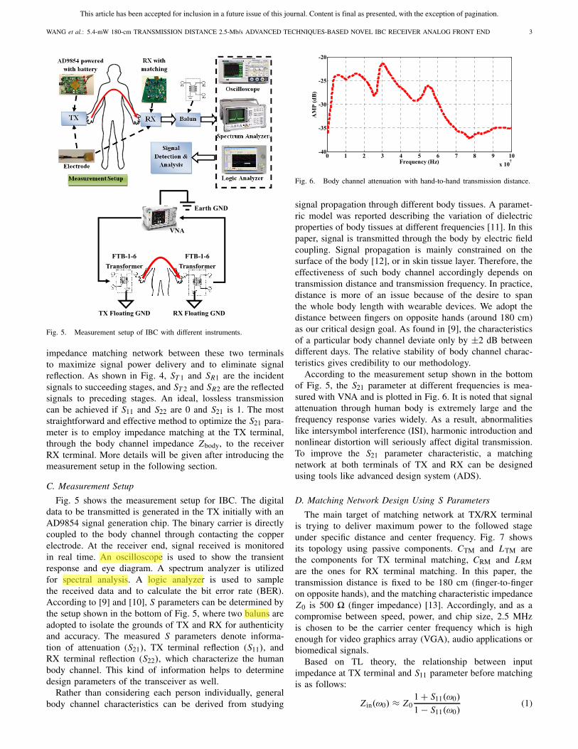
Fig. 5. Measurement setup of IBC with different instruments.
impedance matching network between these two terminalsto maximize signal power delivery and to eliminate signalreflection. As shown in Fig. 4, ST 1 and SR1 are the incidentsignals to succeeding stages, and ST 2 and SR2 are the reflectedsignals to preceding stages. An ideal, lossless transmissioncan be achieved if S11 and S22 are 0 and S21 is 1. The moststraightforward and effective method to optimize the S21 para-meter is to employ impedance matching at the TX terminal,through the body channel impedance Zbody, to the receiverRX terminal. More details will be given after introducing themeasurement setup in the following section.
C. Measurement Setup
Fig. 5 shows the measurement setup for IBC. The digitaldata to be transmitted is generated in the TX initially with anAD9854 signal generation chip. The binary carrier is directlycoupled to the body channel through contacting the copperelectrode. At the receiver end, signal received is monitoredin real time. An oscilloscope is used to show the transientresponse and eye diagram. A spectrum analyzer is utilizedfor spectral analysis. A logic analyzer is used to samplethe received data and to calculate the bit error rate (BER).According to [9] and [10], S parameters can be determined bythe setup shown in the bottom of Fig. 5, where two baluns areadopted to isolate the grounds of TX and RX for authenticityand accuracy. The measured S parameters denote informa-tion of attenuation (S21), TX terminal reflection (S11), andRX terminal reflection (S22), which characterize the humanbody channel. This kind of information helps to determinedesign parameters of the transceiver as well.
Rather than considering each person individually, generalbody channel characteristics can be derived from studying
Fig. 6. Body channel attenuation with hand-to-hand transmission distance.
signal propagation through different body tissues. A paramet-ric model was reported describing the variation of dielectricproperties of body tissues at different frequencies [11]. In thispaper, signal is transmitted through the body by electric fieldcoupling. Signal propagation is mainly constrained on thesurface of the body [12], or in skin tissue layer. Therefore, theeffectiveness of such body channel accordingly depends ontransmission distance and transmission frequency. In practice,distance is more of an issue because of the desire to spanthe whole body length with wearable devices. We adopt thedistance between fingers on opposite hands (around 180 cm)as our critical design goal. As found in [9], the characteristicsof a particular body channel deviate only by ±2 dB betweendifferent days. The relative stability of body channel charac-teristics gives credibility to our methodology.
According to the measurement setup shown in the bottomof Fig. 5, the S21 parameter at different frequencies is mea-sured with VNA and is plotted in Fig. 6. It is noted that signalattenuation through human body is extremely large and thefrequency response varies widely. As a result, abnormalitieslike intersymbol interference (ISI), harmonic introduction andnonlinear distortion will seriously affect digital transmission.To improve the S21 parameter characteristic, a matchingnetwork at both terminals of TX and RX can be designedusing tools like advanced design system (ADS).
D. Matching Network Design Using S Parameters
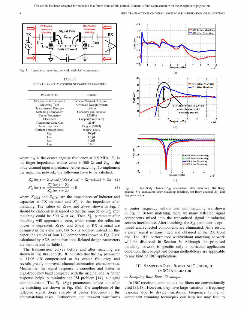
The main target of matching network at TX/RX terminalis trying to deliver maximum power to the followed stageunder specific distance and center frequency. Fig. 7 showsits topology using passive components. CTM and LTM arethe components for TX terminal matching, CRM and LRMare the ones for RX terminal matching. In this paper, thetransmission distance is fixed to be 180 cm (finger-to-fingeron opposite hands), and the matching characteristic impedanceZ0 is 500 � (finger impedance) [13]. Accordingly, and as acompromise between speed, power, and chip size, 2.5 MHzis chosen to be the carrier center frequency which is highenough for video graphics array (VGA), audio applications orbiomedical signals.
Based on TL theory, the relationship between inputimpedance at TX terminal and S11 parameter before matchingis as follows:
Z in(ω0) ≈ Z01 + S11(ω0)
1 − S11(ω0)(1)
Nguyen
Texte surligné
Nguyen
Texte surligné
Nguyen
Texte surligné
Nguyen
Texte surligné
This article has been accepted for inclusion in a future issue of this journal. Content is final as presented, with the exception of pagination.
4 IEEE TRANSACTIONS ON VERY LARGE SCALE INTEGRATION (VLSI) SYSTEMS
Fig. 7. Impedance matching network with LC components.
TABLE I
BODY CHANNEL MATCHING NETWORK PARAMETERS
where ω0 is the center angular frequency at 2.5 MHz, Z0 isthe finger impedance, whose value is 500 �, and Z in is thebody channel input impedance before matching. To implementthe matching network, the following have to be satisfied:
Z∗in(ω0) = Z in(ω0)//ZLTM(ω0) + ZCTM(ω0) ≈ Z0 (2)
S∗11(ω0) = Z∗
in(ω0) − Z0
Z∗in(ω0) + Z0
≈ 0 (3)
where ZLTM and ZCTM are the impedances of inductor andcapacitor at TX terminal and Z∗
in is the impedance aftermatching. The values of ZLTM and ZCTM shown in Fig. 7should be elaborately designed so that the impedance Z∗
in aftermatching could be 500 � at ω0. Then S∗
11 parameter aftermatching will approach to zero, which means the reflectionpower is depressed. ZLRM and ZCRM at RX terminal aredesigned in the same way, but S22 is adopted instead. In thispaper, the values of four LC components shown in Fig. 7 arecalculated by ADS smith chart tool. Related design parametersare summarized in Table I.
The transmission curves before and after matching areshown in Fig. 8(a) and (b). It indicates that the S21 parameteris 11.06 dB compensated at its center frequency andreveals greatly improved channel attenuation characteristics.Meanwhile, the signal response is smoother and flatter inhigh-frequency band compared with the original one. A flatterresponse helps to minimize the ISI problem [14] in digitalcommunication. The S11 (S22) parameters before and afterthe matching are shown in Fig. 8(c). The amplitude of thereflected signal drops sharply at center frequency in theafter-matching cases. Furthermore, the transient waveforms
Fig. 8. (a) Body channel S21 attenuation after matching. (b) Bodychannel S21 attenuation after matching (scaling). (c) Body channel S11 andS22 parameters.
at center frequency without and with matching are shownin Fig. 9. Before matching, there are many reflected signalcomponents mixed into the transmitted signal introducingserious interference. After matching, the S21 parameter is opti-mized and reflected components are eliminated. As a result,a purer signal is transmitted and obtained at the RX frontend. The RFE performance with/without matching networkwill be discussed in Section V. Although the proposedmatching network is specific only a particular applicationcondition, the concept and design methodology are applicableto any kind of IBC applications.
III. SAMPLING RATE BOOSTING TECHNIQUE
IN SC INTEGRATOR
A. Sampling Rate Boost Technique
In IBC receivers, continuous time filters are conventionallyused [3], [8]. However, they have large variation in frequencyresponse due to device variations. Frequency tuning orcomponent trimming techniques can help but may lead to

This article has been accepted for inclusion in a future issue of this journal. Content is final as presented, with the exception of pagination.
WANG et al.: 5.4-mW 180-cm TRANSMISSION DISTANCE 2.5-Mb/s ADVANCED TECHNIQUES-BASED NOVEL IBC RECEIVER ANALOG FRONT END 5
Fig. 9. Received signal without and with matching network.
larger chip size, worse nonlinearity, and higher cost. To addressthis issue, a SC filter is used in our IBC receiver for betterdevice matching, higher accuracy, and lower power consump-tion, benefiting long-distance IBC applications suffering fromlarge signal attenuation and noise power.
Using SC integrator, nonoverlapped clocks are normallyemployed to define two circuit states: sample and hold. Theoperational amplifier (OP-amp) involved is thus idle in half ofthe clock cycle resulting in power inefficiency. Our solutionis based on the double sampling technique in [15] to improvethe power efficiency and obviously the sampling rate as well.However, double sampling is still constrained by the systemclock at high data rate. We further advocate the use ofmultiinterleaved clocks (four for example) with the samefrequency but active at different phases so that the samplingrate is boosted by a factor equal to the number of interleavedclocks. Intuitively, the concept can be expanded to arbitrarysampling rate boosting if more interleaved system clocks areadopted. Therefore, the proposed technique is not a mereextension of double sampling. An analysis with four-timesampling rate boosting is given to elaborate the technique.This technique is first proposed and applied to the RFEin [16]. However, the absence of analysis considering nonidealconditions such as OP-amp finite gain, capacitors mismatch,and noise means its usefulness is doubtful. To make matterworse, an incomplete receiver structure is given in [16] (onlybiquad filter is utilized) offering unattractive performance andtherefore inappropriate for high-performance IBC applications.These problems will be addressed in this paper one by oneleading to a novel and robust receiver front end structureproposed in Section IV.
Fig. 10 shows a SC integrator implemented with thefour-time sampling rate boosting technique. Whenever the con-trolling clocks Ph1, Ph2, Ph3, and Ph4 go high, the switchesare closed. The capacitors in all four branches should havethe same value (mismatch will be discussed later). Its timingsetup is also shown in Fig. 10, where Ph1–Ph4 are controllingsignals of the same frequency but have different phases.Applying the principle of charge conservation, we can derive atransfer function H (z) for the SC integrator. Take the delayednoninverting SC integrator shown in Fig. 11 as an example;at time [n − 2/4]−, branch 3 has already transferred thesampled charge. Thus, considering branch 4 alone, we can
Fig. 10. Proposed four-time sampling rate boost integrator.
Fig. 11. Behavior analysis at time [n − 2/4]−.
write
C1Vin
[n − 3
4
]
CF+ Vout
[n − 3
4
]= Vout
[n − 2
4
](4)
and after z-transform, it becomes
H (z) = C1
CF· z− 3
4
z− 24 − z− 3
4
= C1
CFz− 1
4 · 1
1 − z− 14
(5)
and let z−(1/4) ≈ exp[−(1/4)sT ] ≈ 1 − (1/4)sT to give
H (s) = C1
CF
(1 − 1
4sT
)1
14 sT
≈ C1
CF
114 sT
, sT � 1. (6)
Similarly, the transfer function of a nondelayed inverting typeintegrator can also be derived. In this case, only branch 2needs to be considered at time [n − 2/4]−
H (z) = − C1
CF· z− 2
4
z− 24 − z− 3
4
= − C1
CF· 1
1 − z− 14
(7)
This article has been accepted for inclusion in a future issue of this journal. Content is final as presented, with the exception of pagination.
6 IEEE TRANSACTIONS ON VERY LARGE SCALE INTEGRATION (VLSI) SYSTEMS
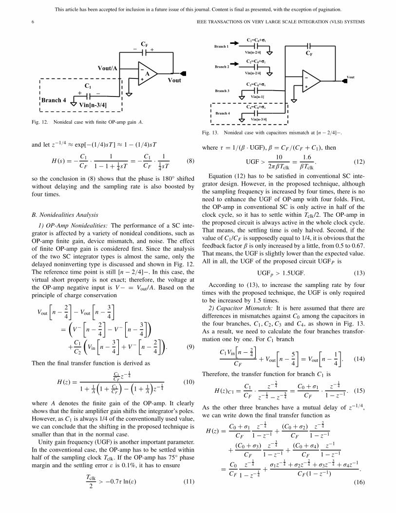
Fig. 12. Nonideal case with finite OP-amp gain A.
and let z−1/4 ≈ exp[−(1/4)sT ] ≈ 1 − (1/4)sT
H (s) = − C1
CF· 1
1 − 1 + 14 sT
= − C1
CF· 1
14 sT
(8)
so the conclusion in (8) shows that the phase is 180° shiftedwithout delaying and the sampling rate is also boosted byfour times.
B. Nonidealities Analysis
1) OP-Amp Nonidealities: The performance of a SC inte-grator is affected by a variety of nonideal conditions, such asOP-amp finite gain, device mismatch, and noise. The effectof finite OP-amp gain is considered first. Since the analysisof the two SC integrator types is almost the same, only thedelayed noninverting type is discussed and shown in Fig. 12.The reference time point is still [n − 2/4]−. In this case, thevirtual short property is not exact; therefore, the voltage atthe OP-amp negative input is V − = Vout/A. Based on theprinciple of charge conservation
Vout
[n − 2
4
]− Vout
[n − 3
4
]
=(
V −[
n − 2
4
]− V −
[n − 3
4
])
+C1
C2
(Vin
[n − 3
4
]+ V −
[n − 2
4
]). (9)
Then the final transfer function is derived as
H (z) =C1CF
z− 14
1 + 1A
(1 + C1
CF
)−
(1 + 1
A
)z− 1
4
(10)
where A denotes the finite gain of the OP-amp. It clearlyshows that the finite amplifier gain shifts the integrator’s poles.However, as C1 is always 1/4 of the conventionally used value,we can conclude that the shifting in the proposed technique issmaller than that in the normal case.
Unity gain frequency (UGF) is another important parameter.In the conventional case, the OP-amp has to be settled withinhalf of the sampling clock Tclk. If the OP-amp has 75° phasemargin and the settling error ε is 0.1%, it has to ensure
Tclk
2> −0.7τ ln(ε) (11)
Fig. 13. Nonideal case with capacitors mismatch at [n − 2/4]−.
where τ = 1/(β · UGF), β = CF /(CF + C1), then
UGF >10
2πβTclk= 1.6
βTclk. (12)
Equation (12) has to be satisfied in conventional SC inte-grator design. However, in the proposed technique, althoughthe sampling frequency is increased by four times, there is noneed to enhance the UGF of OP-amp with four folds. First,the OP-amp in conventional SC is only active in half of theclock cycle, so it has to settle within Tclk/2. The OP-amp inthe proposed circuit is always active in the whole clock cycle.That means, the settling time is only halved. Second, if thevalue of C1/CF is supposedly equal to 1/4, it is obvious that thefeedback factor β is only increased by a little, from 0.5 to 0.67.That means, the UGF is slightly lower than the expected value.All in all, the UGF of the proposed circuit UGFP is
UGFp > 1.5UGF. (13)
According to (13), to increase the sampling rate by fourtimes with the proposed technique, the UGF is only requiredto be increased by 1.5 times.
2) Capacitor Mismatch: It is here assumed that there aredifferences in mismatches against C0 among the capacitors inthe four branches, C1, C2, C3 and C4, as shown in Fig. 13.As a result, we need to calculate the four branches transfor-mation one by one. For C1 branch
C1Vin
[n − 2
4
]
CF+ Vout
[n − 5
4
]= Vout
[n − 1
4
]. (14)
Therefore, the transfer function for branch C1 is
H (z)C1 = C1
CF· z− 2
4
z− 14 − z− 5
4
= C0 + σ1
CF· z− 1
4
1 − z−1 . (15)
As the other three branches have a mutual delay of z−1/4,we can write down the final transfer function as
H (z) = C0 + σ1
CF
z− 14
1 − z−1 + (C0 + σ2)
CF
z− 24
1 − z−1
+ (C0 + σ3)
CF
z− 34
1 − z−1 + (C0 + σ4)
CF
z−1
1 − z−1
= C0
CF
z− 14
1 − z− 14
+ σ1z− 14 + σ2z− 2
4 + σ3z− 34 + σ4z−1
CF (1 − z−1).
(16)

This article has been accepted for inclusion in a future issue of this journal. Content is final as presented, with the exception of pagination.
WANG et al.: 5.4-mW 180-cm TRANSMISSION DISTANCE 2.5-Mb/s ADVANCED TECHNIQUES-BASED NOVEL IBC RECEIVER ANALOG FRONT END 7
Fig. 14. Nonideal case with output referred noise at [n − 2/4]−.
Considering the s domain
H (s)
= C0
CF
(1 − 1
4 sT)
14 sT
+ σ1(1 − 1
4 sT)+σ2
(1− 2
4 sT) + σ3
(1 − 3
4 st)+σ4(1−sT )
CF sT.
(17)
If the oversampling rate is very large, it gives
H (s) ≈ C0
CF
(1 + 1
4 (σ1 + σ2 + σ3 + σ4))
14 sT
. (18)
Equation (18) shows an interesting result that the mismatchintroduced by the four capacitors is not accumulated, butaveraged by the value of the boosting rate instead. If thesampling rate is boosted by n times, its general expressionbecomes
H (s) ≈ C0
CF
(1 + 1
n ni=1 σi
)
1n sT
. (19)
In conclusion, if there is no mismatch, the transmissionfunction is the same as (6). As the mismatch is due to thediscrepancy in the relative sizes of the capacitors, its effecton the circuit is negligible compared with the absolute valuemismatch in the RC integrator. Furthermore, increasing thevalue of CF can also minimize the mismatch effectively.
3) Noise Analysis: Noise is another important parameter toconsider for this proposed technique. Noise of SC integratorsis attributable to three means: 1) sampling phase kT /C noiseof switches; 2) amplifying phase kT /C noise of switches; and3) OP-amp noise. We also take [n − 2/4]− time point asan example and the equivalent circuit is shown in Fig. 14,where branch 4 is in amplifying phase (branch 3 has finishedamplifying and settled). Rs denotes the resistance of switches.Vns4 denotes the noise source introduced by switch resistorsin branch 4. Va denotes the noise caused by OP-amp. Overthe sampling phase, the switch noise is kT /Ci , where Ci isthe sampling capacitor in the i th branch. In the amplifyingphase, switches noise referring to the output of the integrator
Fig. 15. Topology of conventional threshold comparison-based RFE.
will be
V 2switch =
(C1
CF
)2 kT
C1(20)
where V 2switch is the output referred switch noise. OP-amp
contributes the second part of the output referred noise
V 2OP =
(CF + 4
2 C1
CF
)2
V 2a . (21)
Then the total output referred noise in both phases of onebranch is derived as
V 2o =
(CF + 4
2 C1
CF
)2
V 2a + 2
(C1
CF
)2 kT
C1. (22)
Given the sampling rate is boosted by n times, the outputreferred noise in n branches will be
V 2o = n
(CF+ n
2 C1
CF
)2
V 2a +2n
(C1
CF
)2 kT
C1. (23)
Based on (23), the contribution of OP-amp referring to outputnoise is little enlarged. However, the noise contributed by allswitches of branches is the same as conventional one, becauseC1 is n times smaller. Furthermore, small C1 and large CF
are beneficial to reduce the output noise.
IV. RFE CIRCUIT IMPLEMENTATION
As mentioned earlier, CTD-based RFE processes rawsignal in continuous time domain using a RC filterand a hysteretic comparator. Large power consumption(both static and dynamic) in hysteretic comparator, devicesmismatches, and absolute value variations together meanthat this method is not suitable for high-performanceIBC applications.
However, our proposed RFE uses a sampling rate boostSC biquad filter instead of the conventional RC filter.In addition, a matching integrator [17] is used rather than acomparator, followed by weak signal integration and furthernoise filtering. Both the SC filter and the integrator consumelittle power and achieve reasonably high device matching.A comparison between these two designs demonstrates the
Nguyen
Texte surligné
Nguyen
Texte surligné
This article has been accepted for inclusion in a future issue of this journal. Content is final as presented, with the exception of pagination.
8 IEEE TRANSACTIONS ON VERY LARGE SCALE INTEGRATION (VLSI) SYSTEMS
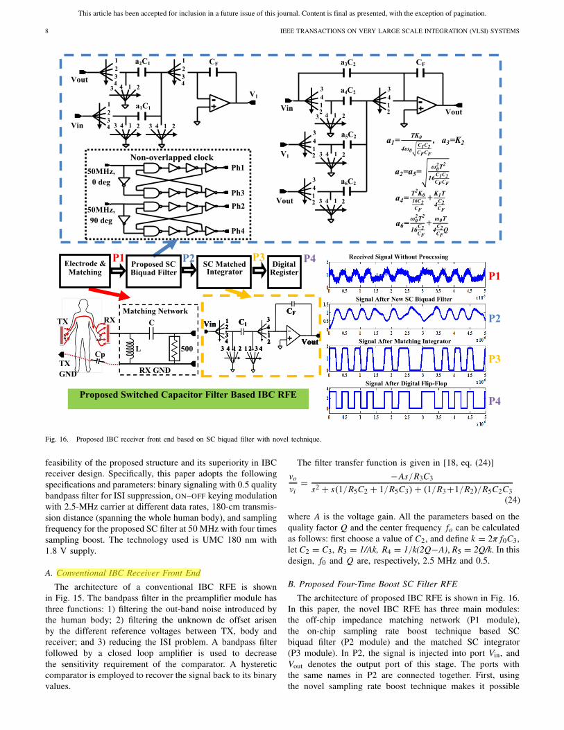
Fig. 16. Proposed IBC receiver front end based on SC biquad filter with novel technique.
feasibility of the proposed structure and its superiority in IBCreceiver design. Specifically, this paper adopts the followingspecifications and parameters: binary signaling with 0.5 qualitybandpass filter for ISI suppression, ON–OFF keying modulationwith 2.5-MHz carrier at different data rates, 180-cm transmis-sion distance (spanning the whole human body), and samplingfrequency for the proposed SC filter at 50 MHz with four timessampling boost. The technology used is UMC 180 nm with1.8 V supply.
A. Conventional IBC Receiver Front End
The architecture of a conventional IBC RFE is shownin Fig. 15. The bandpass filter in the preamplifier module hasthree functions: 1) filtering the out-band noise introduced bythe human body; 2) filtering the unknown dc offset arisenby the different reference voltages between TX, body andreceiver; and 3) reducing the ISI problem. A bandpass filterfollowed by a closed loop amplifier is used to decreasethe sensitivity requirement of the comparator. A hystereticcomparator is employed to recover the signal back to its binaryvalues.
The filter transfer function is given in [18, eq. (24)]
vo
vi= −As/R3C3
s2 + s(1/R5C2 + 1/R5C3) + (1/R3+1/R2)/R5C2C3(24)
where A is the voltage gain. All the parameters based on thequality factor Q and the center frequency fo can be calculatedas follows: first choose a value of C2, and define k = 2π f0C3,let C2 = C3, R3 = 1/Ak, R4 = 1/k(2Q−A), R5 = 2Q/k. In thisdesign, f0 and Q are, respectively, 2.5 MHz and 0.5.
B. Proposed Four-Time Boost SC Filter RFE
The architecture of proposed IBC RFE is shown in Fig. 16.In this paper, the novel IBC RFE has three main modules:the off-chip impedance matching network (P1 module),the on-chip sampling rate boost technique based SCbiquad filter (P2 module) and the matched SC integrator(P3 module). In P2, the signal is injected into port Vin, andVout denotes the output port of this stage. The ports withthe same names in P2 are connected together. First, usingthe novel sampling rate boost technique makes it possible
Nguyen
Texte surligné
This article has been accepted for inclusion in a future issue of this journal. Content is final as presented, with the exception of pagination.
WANG et al.: 5.4-mW 180-cm TRANSMISSION DISTANCE 2.5-Mb/s ADVANCED TECHNIQUES-BASED NOVEL IBC RECEIVER ANALOG FRONT END 9
for the SC circuit to work at high frequency ensured by theoversampling ratio. Second, the SC biquad filter replacesthe conventional RC bandpass filter effectively increasingmatching quality and minimizing ISI. Third, the weakreceived signal after the SC biquad filter will be amplified tosupply rail level and will then be recovered to binary valuesby a matched integrator based on the proposed sampling boosttechnique along with greatly decreased power consumptioncompared with the hysteretic comparator. The behavior andhence the feasibility of each module (P1 ∼ P4) are provedby transient simulation. For realistic simulation, the input rawsignal is obtained directly from in situ measurements.
A conventional biquad SC filter was discussed in [19].Its transmission function can be expressed as
H (s) = Vout(s)
Vin(s)= − (K2s2 + K1s + K0)
s2 + ω0Q s + ω2
0
(25)
where ω0 denotes the center angular frequency,K0, K1, and K2 decide the location of zeros and gain,and Q is the quality factor. Then combining this structurewith the proposed oversampling technique, a novel four-timesampling biquad filter is shown in Fig. 16.
In Fig. 16, based on (5) and (7), the expressions at nodesV1 and Vout are as follows:
V1 = −C1CF
a1
1 − z− 14
Vin −C1CF
a2
1 − z− 14
Vout (26)
Vout = −a3Vin −C2CF
a4
1 − z− 14
Vin + a5C2CF
z− 14 V1
1 − z− 14
−C2CF
a6Vout
1 − z− 14
(27)
and then
H (s) = Vout
Vin
= −s2a3 +
(4 C2
CFa4
T − 4a1a5C1CF
C2CF
T
)s + 16a1a5
C1CF
C2CF
T 2
s2 +(
4 C2CF
a6
T − 4a2a5C1CF
C2CF
T
)s + 16a2a5
C1CF
C2CF
T 2
(28)
where T is the sampling frequency and the values of a1, a2,a3, a4, a5, and a6 can be calculated based on the equationsin Fig. 16.
The four-phase nonoverlap clocks are generated withLeCroy arbitrary signal generator in this paper. The in-phaseand the 90° out-of-phase 50-MHz clocks are buffered withtapered inverter chains on chip to generate the nonoverlapgaps, as shown in Fig. 16. For higher than four times samplingrate boost cases, the interleaved clocks can be easily realizedwith a cascaded ring oscillator [20]. The details will not bediscussed in this paper.
For wearable and wireless sensor networks, energy harvest-ing could be used for obvious benefits and for bringing IBCinto more practical applications. Suitable energy harvesters arediscussed in [21] and [22]. In this paper, our aim is to prove thefeasibility of the proposed SC technique based on impedance
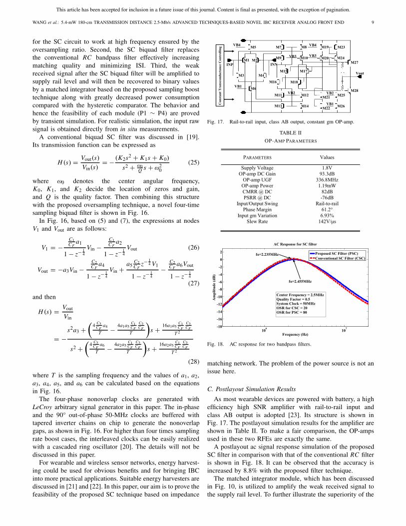
Fig. 17. Rail-to-rail input, class AB output, constant gm OP-amp.
TABLE II
OP-AMP PARAMETERS
Fig. 18. AC response for two bandpass filters.
matching network. The problem of the power source is not anissue here.
C. Postlayout Simulation Results
As most wearable devices are powered with battery, a highefficiency high SNR amplifier with rail-to-rail input andclass AB output is adopted [23]. Its structure is shown inFig. 17. The postlayout simulation results for the amplifier areshown in Table II. To make a fair comparison, the OP-ampsused in these two RFEs are exactly the same.
A postlayout ac signal response simulation of the proposedSC filter in comparison with that of the conventional RC filteris shown in Fig. 18. It can be observed that the accuracy isincreased by 8.8% with the proposed filter technique.
The matched integrator module, which has been discussedin Fig. 10, is utilized to amplify the weak received signal tothe supply rail level. To further illustrate the superiority of the

This article has been accepted for inclusion in a future issue of this journal. Content is final as presented, with the exception of pagination.
10 IEEE TRANSACTIONS ON VERY LARGE SCALE INTEGRATION (VLSI) SYSTEMS
Fig. 19. DC transient with proposed and conventional SC integrator.
Fig. 20. Microphotograph of proposed (left) and conventional (right) RFEs.
Fig. 21. Measurement test boards of TX and RX.
proposed sampling boost technique, a postlayout simulationwith 20-mV dc input for this integrator is shown in Fig. 19.By the use of the proposed technique, the integration ismore accurate and closer to its ideal integration result. Eventhough both of these two designs in Fig. 19 employ the sameOP-amp, the proposed technique has been less affected by thenonidealities of the amplifier.
V. IBC CHIP MEASUREMENT
The two RFEs were fabricated in a 0.18-μm CMOS processand the chip microphotographs are shown in Fig. 20. The corearea of the proposed RFE is 0.706 mm2, and the conventionalRFE is 0.464 mm2. The measurement test board is shownin Fig. 21. The TX on the left hand side is a battery poweredAD9854. It generates signals with different amplitudes andfrequencies. On the right-hand side is the testing PCB boardof the IBC RFE chip with off-chip matching network andregulators.
Fig. 22. Measurement setup with hand-to-hand touching.
Fig. 23. Transient waveform of proposed IBC RFE.
TABLE III
RECEIVER FRONT END MEASUREMENT
A subject with two-hand span of approximately 180 cmwas holding the electrodes (TX end and RX end), as shownin Fig. 22. During transmission, an oscilloscope and a logicanalyzer were used to detect and measure the transmissionperformance. The transient waveform is shown in Fig. 23. Thetransmitted signal is 2.5 Mb/s with 2.5-MHz carrier, 1.2 Vamplitude. Before recovery, the raw signal is weak with arange of 40 mV and very noisy, and after processing by theproposed IBC RFE, the signal is recovered fully and noisefree.
BER is an important specification to quantify the reliabilityof a communication system. Curves of BER versus differ-ent data rates with 180-cm transmission distance are shown

This article has been accepted for inclusion in a future issue of this journal. Content is final as presented, with the exception of pagination.
WANG et al.: 5.4-mW 180-cm TRANSMISSION DISTANCE 2.5-Mb/s ADVANCED TECHNIQUES-BASED NOVEL IBC RECEIVER ANALOG FRONT END 11
TABLE IV
PARAMETERS COMPARISON
Fig. 24. BER comparison versus different data rates without matching.
Fig. 25. BER comparison versus different data rates with matching.
in Figs. 24 and 25. The measurement results prove that byintroducing the matching network, the minimum BER canbe enhanced by nearly one order of magnitude, and the newRFE can reach 1e-7 at 2.5 Mb/s, which is much less thanthat found in the conventional RFE with 3e-7. A functionalsummary of the proposed RFE is shown in Table III and acomparison with other similar designs is shown in Table IV.To make a reasonable comparison and stress the importance ofthe transmission distance, a distance-figure-of-merit (DFOM)is defined, which is calculated as
DFOM = BER × Power
Distance × Data Rate. (29)
DFOM can identify a better all-round design consideringBER, power, transmission distance, and data rate together,the parameters that play significant roles in IBC design.It indicates how much energy per meter and per bit is used inunits of fJ/(m · bit) along with the achieved BER.
Using the DFOM as a figure for comparison, the proposedSCF RFE outperforms all other referred designs with only0.12 fJ/(m · bit), validating the feasibility and the promisingrole the new proposed technique can take in future IBC devel-opment.
VI. CONCLUSION
This paper has proposed a new approach to deal withbody communication channel modeling based on TL theory.A matching network was designed to optimize the transmis-sion S21 parameter, which plays a significant role in IBCreceiver design. Furthermore, a new sampling rate boostingtechnique has been proposed and applied to a SC filter toincrease its operation frequency and accuracy. An IBC RFEbased on the proposed techniques, together with one basedon the conventional threshold comparison method, has beenimplemented in a 0.18-μm process. Postlayout simulationresults and chip measurement results are given, which show asuperior performance with the proposed RFE over other simi-lar designs. Finally, these results also suggest that the proposedarbitrary sampling rate boosting technique is beneficial notonly in IBC design but also in other related SC circuits designsdemanding high speed or high accuracy, such as delta–sigmamodulators and biomedical sensors.
REFERENCES
[1] N. Cho, J. Yoo, S.-J. Song, J. Lee, S. Jeon, and H.-J. Yoo, “The humanbody characteristics as a signal transmission medium for intrabodycommunication,” IEEE Trans. Microw. Theory Techn., vol. 55, no. 5,pp. 1080–1086, May 2007.
[2] R. Xu, H. Zhu, and J. Yuan, “Electric-field intrabody communicationchannel modeling with finite-element method,” IEEE Trans. Biomed.Eng., vol. 58, no. 3, pp. 705–712, Mar. 2011.
[3] S.-J. Song, N. Cho, S. Kim, and H.-J. Yoo, “A 4.8-mW 10-Mb/swideband signaling receiver analog front-end for human body commu-nications,” in Proc. 32nd Eur. Solid-State Circuits Conf. (ESSCIRC),Sep. 2006, pp. 488–491.

This article has been accepted for inclusion in a future issue of this journal. Content is final as presented, with the exception of pagination.
12 IEEE TRANSACTIONS ON VERY LARGE SCALE INTEGRATION (VLSI) SYSTEMS
[4] A. Nakata et al., “Development and performance analysis ofan intra-body communication device,” in Proc. 12th Int. Conf.TRANSDUCER, Solid-State Sens., Actuators Microsyst., vol. 2.Jun. 2003, pp. 1722–1725.
[5] J. Wang, Y. Nishikawa, and T. Shibata, “Analysis of on-body trans-mission mechanism and characteristic based on an electromagneticfield approach,” IEEE Trans. Microw. Theory Techn., vol. 57, no. 10,pp. 2464–2470, Oct. 2009.
[6] J. A. Ruiz and S. Shimamoto, “Statistical modeling of intra-bodypropagation channel,” in Proc. IEEE Wireless Commun. Netw. Conf.,Mar. 2007, pp. 2063–2068.
[7] J. Bae, H. Cho, K. Song, H. Lee, and H.-J. Yoo, “The signal trans-mission mechanism on the surface of human body for body channelcommunication,” IEEE Trans. Microw. Theory Techn., vol. 60, no. 3,pp. 582–593, Mar. 2012.
[8] S.-J. Song, N. Cho, S. Kim, J. Yoo, and H.-J. Yoo, “A 2Mb/s widebandpulse transceiver with direct-coupled interface for human body commu-nications,” in IEEE ISSCC Dig. Tech. Papers, Feb. 2006, pp. 2278–2287.
[9] M. Amparo Callejon, D. Naranjo-Hernandez, J. Reina-Tosina, andL. M. Roa, “Distributed circuit modeling of galvanic and capacitivecoupling for intrabody communication,” IEEE Trans. Biomed. Eng.,vol. 59, no. 11, pp. 3263–3269, Nov. 2012.
[10] M. A. Callejon, D. Naranjo-Hernandez, J. Reina-Tosina, and L. M. Roa,“A comprehensive study into intrabody communication measurements,”IEEE Trans. Instrum. Meas., vol. 62, no. 9, pp. 2446–2455, Sep. 2013.
[11] S. Gabriel, R. W. Lau, and C. Gabriel, “The dielectric properties ofbiological tissues: III. Parametric models for the dielectric spectrum oftissues,” Phys. Med. Biol., vol. 41, no. 11, pp. 2271–2293, 1996.
[12] M. A. Callejon, L. M. Roa, J. Reina-Tosina, and D. Naranjo-Hernandez,“Study of attenuation and dispersion through the skin in intrabodycommunications systems,” IEEE Trans. Inf. Technol. Biomed., vol. 16,no. 1, pp. 159–165, Jan. 2012.
[13] O. G. Martinsen and S. Grimnes, Bioimpedance and BioelectricityBasics, 2nd ed. San Francisco, CA, USA: Academic, Apr. 2008.
[14] J. G. Proakis and M. Salehi, “Digital communication through band-limited channels,” in Digital Communications, 5th ed. New York, NY,USA: McGraw-Hill, Nov. 2007.
[15] P. J. Hurst and W. J. McIntyre, “Double sampling in switched-capacitordelta-sigma A/D converters,” in Proc. IEEE Int. Symp. Circuits Syst.,May 1990, pp. 902–905.
[16] H. Wang and C. S. Choy, “A novel high speed, low power intrabodycommunication receiver front end based on sampling rate boostingswitched-capacitor filter,” in Proc. IEEE 57th MWSCAS, Aug. 2014,pp. 872–875.
[17] J. Savoj and B. Razavi, “A CMOS interface for detection of1.2-GB/S RZ data,” in High-Speed CMOS Circuits for OpticalReceivers. Boston, MA, USA: Kluwer, 2001, pp. 61–66.
[18] Multiple Feedback Band-Pass Design Example, Analog Device Inc.,Norwood, MA, USA. 2012.
[19] P. E. Allen and D. R. Holberg, CMOS Analog Circuit Design, 2nd ed.London, U.K.: Oxford Univ. Press, 2002, pp. 551–553.
[20] W. S. T. Yan and H. C. Luong, “A 900-MHz CMOS low-phase-noisevoltage-controlled ring oscillator,” IEEE Trans. Circuits Syst. II, AnalogDigit. Signal Process., vol. 48, no. 2, pp. 216–221, Feb. 2001.
[21] J. W. Matiko, N. J. Grabham, S. P. Beeby, and M. J. Tudor, “Review ofthe application of energy harvesting in buildings,” Meas. Sci. Technol.,vol. 25, no. 1, p. 012002, 2014.
[22] B. Li, X. Shao, N. Shahshahan, N. Goldsman, T. Salter, andG. M. Metze, “An antenna co-design dual band RF energy harvester,”IEEE Trans. Circuits Syst. I, Reg. Papers, vol. 60, no. 12, pp. 3256–3266,Dec. 2013.
[23] R. Hogervorst, J. P. Tero, R. G. H. Eschauzier, and J. H. Huijsing,“A compact power-efficient 3 V CMOS rail-to-rail input/output opera-tional amplifier for VLSI cell libraries,” IEEE J. Solid-State Circuits,vol. 29, no. 12, pp. 1505–1513, Dec. 1994.
[24] M. Shinagawa, M. Fukumoto, K. Ochiai, and H. Kyuragi, “A near-field-sensing transceiver for intrabody communication based on the electroop-tic effect,” IEEE Trans. Instrum. Meas., vol. 53, no. 6, pp. 1533–1538,Dec. 2004.
[25] S.-J. Song, N. Cho, and H.-J. Yoo, “A 0.2-mW 2-Mb/s digital transceiverbased on wideband signaling for human body communications,” IEEEJ. Solid-State Circuits, vol. 42, no. 9, pp. 2021–2033, Sep. 2007.
[26] N. Cho, L. Yan, J. Bae, and H.-J. Yoo, “A 60 kb/s–10 Mb/s adaptivefrequency hopping transceiver for interference-resilient body channelcommunication,” IEEE J. Solid-State Circuits, vol. 44, no. 3,pp. 708–717, Mar. 2009.
[27] J. Bae, K. Song, H. Lee, H. Cho, and H.-J. Yoo, “A 0.24-nJ/b wirelessbody-area-network transceiver with scalable double-FSK modulation,”IEEE J. Solid-State Circuits, vol. 47, no. 1, pp. 310–322, Jan. 2012.
Hao Wang (S’13) was born in Jilin, China.He received the bachelor’s degree from theDepartment of Information Science and ElectronicEngineering, Zhejiang University, Hangzhou, China,in 2010. He is currently pursuing the Ph.D. degree inelectronic engineering from the Chinese Universityof Hong Kong (CUHK), Hong Kong.
He is currently with the ASIC Laboratory,Department of Electronic Engineering, CUHK. He isalso with the Mixed-Signal Biomedical IntegratedCircuit Group. His current research interests include
mixed-signal biomedical integrated circuits design, field-programmable gatearray, and digital communication system design.
Xian Tang (S’08–M’14) received the bachelor’sdegree in electronic science and technology fromthe Huazhong University of Science and Technology,Wuhan, China, in 2007, and the Ph.D. degree inelectronic engineering from the Chinese Universityof Hong Kong, Hong Kong, in 2013.
She was an International Visiting Student withthe University of Toronto, Toronto, ON, Canada, in2011. She is currently an Assistant Professor withthe Division of Information Science and Technology,Graduate School at Shenzhen, Tsinghua University,
Shenzhen, China. Her current research interests include CMOS analog/mixed-signal integrated circuits design, in particular, pipelined analog-to-digitalconverters, temperature sensors, and power management integrated circuits.
Dr. Tang was a recipient of the Global Scholarship Program for ResearchExcellence-CNOOC Grants 2010–2011 from the Chinese University ofHong Kong in 2010, and the Student Travel Grant Award from the IEEE Solid-State Society and the International Solid-State Circuits Conference in 2012.
Chiu Sing Choy received the B.Sc., M.Sc., andPh.D. degrees in electrical and electronics engineer-ing from the University of Manchester, Manchester,U.K., in 1983, 1984, and 1987, respectively.
He spent a year with Ferranti Microelectron-ics, Oldham, U.K., where he participated inapplication-specified integrated circuit technology(ASIC) research. In 1986, he joined the Departmentof Electronic Engineering, Chinese University ofHong Kong, Hong Kong, where he is currentlya Professor. His current research interests include
network-on-chip, body area network, structured ASIC, OFDM-UWB digitaltransceiver, real-time object detection, high-performance arithmetic units withreduced precision, and IEEG signal processing and deep learning designs.
Prof. Choy is a fellow of The Hong Kong Institution of Engineers (HKIE).He was the Chairperson of the Electronics Division in 2006 and 2007 and aCouncil Member of HKIE.

This article has been accepted for inclusion in a future issue of this journal. Content is final as presented, with the exception of pagination.
WANG et al.: 5.4-mW 180-cm TRANSMISSION DISTANCE 2.5-Mb/s ADVANCED TECHNIQUES-BASED NOVEL IBC RECEIVER ANALOG FRONT END 13
Ka Nang Leung (S’02–M’03–SM’08) receivedthe B.Eng., M.Phil., and Ph.D. degrees from theDepartment of Electronic and Computer Engineer-ing, Hong Kong University of Science and Tech-nology (HKUST), Hong Kong, all in electrical andelectronic engineering.
He was with HKUST in 2002, where he becamea Visiting Assistant Professor. After three years ofservice with HKUST, he joined the Departmentof Electronic Engineering, Chinese University ofHong Kong, Hong Kong, in 2005, where he is
currently an Associate Professor. His current research interests includepower-management integrated circuits and low-voltage low-power analogueintegrated circuits.
Prof. Leung was the Chairman of the IEEE (Hong Kong) ElectronDevice/Solid-State Circuit Joint Chapter in 2012. He serves on the EditorialBoard of Active and Passive Electronic Components, Hindawi PublishingCorporation, Cairo, Egypt, and also serves as a paper reviewer in numerousIEEE and the Institution of Engineering and Technology journals and inter-national conferences. He is actively involved in the organization of severalIEEE international conferences.
Kong Pang Pun (S’97–M’01–SM’09) receivedthe B.Eng. and M.Phil. degrees in electronicsengineering from the Chinese University ofHong Kong (CUHK), Hong Kong, in 1995 and 1997,respectively, and the Ph.D. degree in electrical andcomputer engineering from the Instituto SuperiorTécnico, Technical University of Lisbon, Lisbon,Portugal, in 2001.
He is currently an Associate Professor with theDepartment of Electronic Engineering, CUHK.His current research interests include CMOS
analog/mixed-signal integrated circuits design, in particular, high-energy-efficiency analog-to-digital converters, ultralow voltage circuits, sensorinterface circuits, and complex signal processing circuits.
Dr. Pun received the Exemplary Teaching Awards from the Faculty ofEngineering, CUHK, in 2005, 2010, and 2013. He served as the Chairmanof the IEEE Hong Kong Joint-Chapter of Electron Devices and Solid-StateCircuits in 2008 and 2009. He was the General Co-Chair of the IEEEInternational Conference on Electron Devices and Solid-State Circuits in2008, and a member of the International Technical Committee of the IEEEInternational Solid State Circuits Conference from 2008 to 2012. He will bea Co-Guest Editor of the IEEE JOURNAL ON EMERGING AND SELECTED
TOPICS IN CIRCUITS AND SYSTEMS 2015 Special Issue on Next-GenerationDelta-Sigma Converters.