A 32 nm, 3.1 billion transistor, 12 wide issue Itanium...
30
A 32 nm, 3.1 billion transistor, 12 wide issue Itanium® Processor for Mission-Critical Servers Reid Riedlinger 1 , Rohit Bhatia 1 , Larry Biro 2 , Bill Bowhill 2 , Eric Fetzer 1 , Paul Gronowski 2 , Tom Grutkowski 1 1 Intel® Corporation, Fort Collins, CO 2 Intel® Corporation, Hudson, MA © 2011 IEEE IEEE International Solid-State Circuits Conference © 2011 IEEE
Transcript of A 32 nm, 3.1 billion transistor, 12 wide issue Itanium...
A 32 nm, 3.1 billion transistor,12 wide issue Itanium® Processor
for Mission-Critical Servers
Reid Riedlinger1, Rohit Bhatia1, Larry Biro2,Bill Bowhill2, Eric Fetzer1,
Paul Gronowski2, Tom Grutkowski11Intel® Corporation, Fort Collins, CO
2Intel® Corporation, Hudson, MA
© 2011 IEEE IEEE International Solid-State Circuits Conference © 2011 IEEE
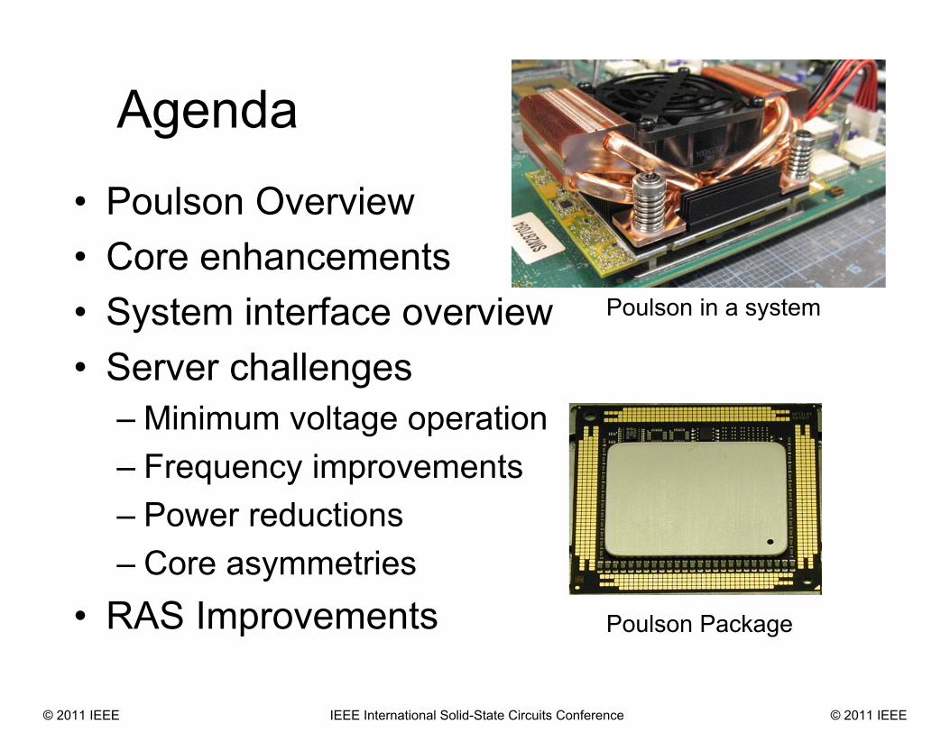
Agenda• Poulson Overview• Core enhancements• System interface overview• Server challenges
– Minimum voltage operation– Frequency improvements– Power reductions– Core asymmetries
• RAS Improvements Poulson Package
Poulson in a system
© 2011 IEEE IEEE International Solid-State Circuits Conference © 2011 IEEE
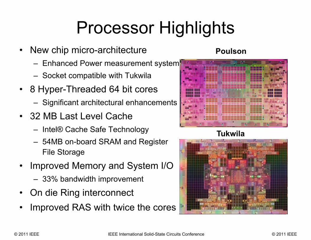
Processor Highlights• New chip micro-architecture
– Enhanced Power measurement system – Socket compatible with Tukwila
• 8 Hyper-Threaded 64 bit cores– Significant architectural enhancements
• 32 MB Last Level Cache– Intel® Cache Safe Technology– 54MB on-board SRAM and Register
File Storage
• Improved Memory and System I/O– 33% bandwidth improvement
• On die Ring interconnect • Improved RAS with twice the cores
Poulson
Tukwila
© 2011 IEEE IEEE International Solid-State Circuits Conference © 2011 IEEE
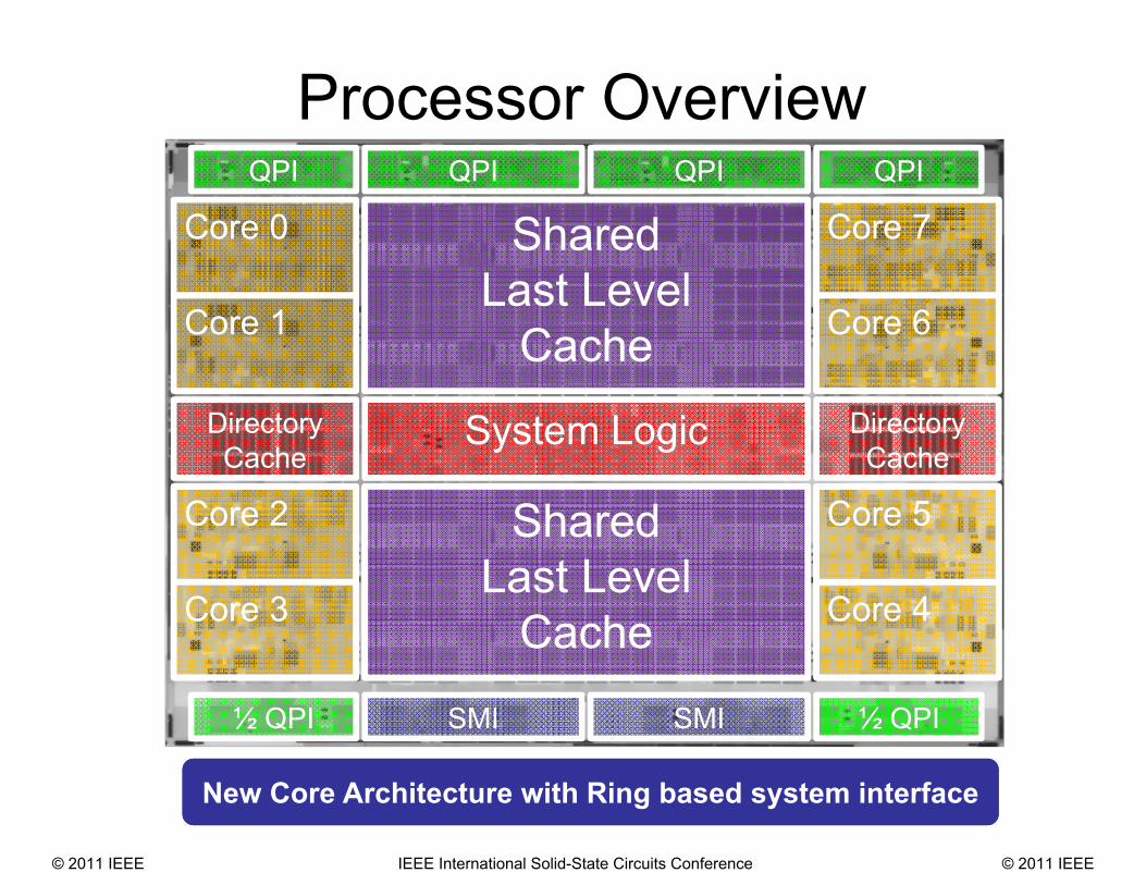
Processor Overview
Core 0
Directory Cache
Directory Cache
System Logic
QPI QPIQPI QPI
SMI SMI ½ QPI½ QPI
SharedLast Level
CacheCore 1
Core 2
Core 3 Core 4
Core 5
Core 7
Core 6
SharedLast Level
Cache
New Core Architecture with Ring based system interface
© 2011 IEEE IEEE International Solid-State Circuits Conference © 2011 IEEE
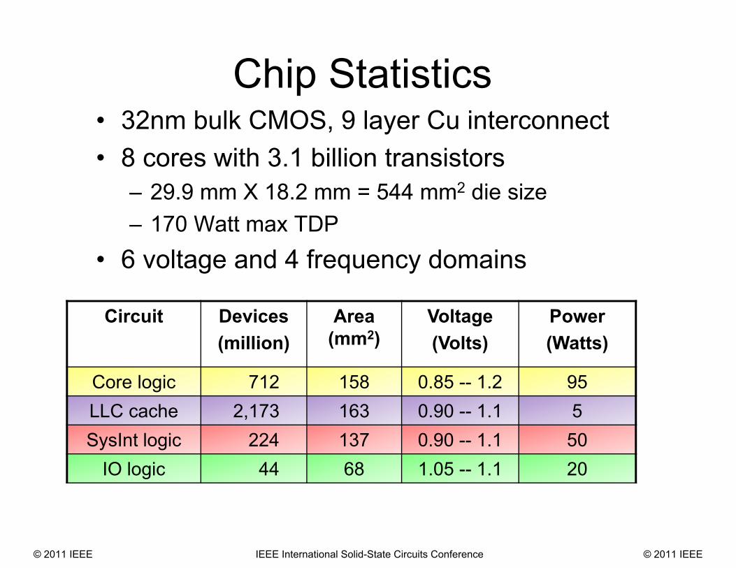
Chip Statistics• 32nm bulk CMOS, 9 layer Cu interconnect• 8 cores with 3.1 billion transistors
– 29.9 mm X 18.2 mm = 544 mm2 die size– 170 Watt max TDP
• 6 voltage and 4 frequency domains
Circuit Devices(million)
Area (mm2)
Voltage(Volts)
Power(Watts)
Core logic 712 158 0.85 -- 1.2 95 LLC cache 2,173 163 0.90 -- 1.1 5SysInt logic 224 137 0.90 -- 1.1 50
IO logic 44 68 1.05 -- 1.1 20
© 2011 IEEE IEEE International Solid-State Circuits Conference © 2011 IEEE
Core Design• Micro-architecture and floor plan optimized for future
process generations– First comprehensive redesign of IPF core since Itanium 2 design
(McKinley)– RC minimization of critical core signals
• Design methodology that enables process scaling– Emphasis on power reduction, higher frequency, low voltage
operation, and high yield– Elimination of dynamic logic outside of RF topologies
• Decoupling buffer between Instruction fetch and execution– Holds 96 instructions – replicated per thread
• Replay versus Stall design– Significant power reduction across all work loads– Instruction buffer acts as replay point for backend execution– Commit, exception and stall timing made easier
© 2011 IEEE IEEE International Solid-State Circuits Conference © 2011 IEEE
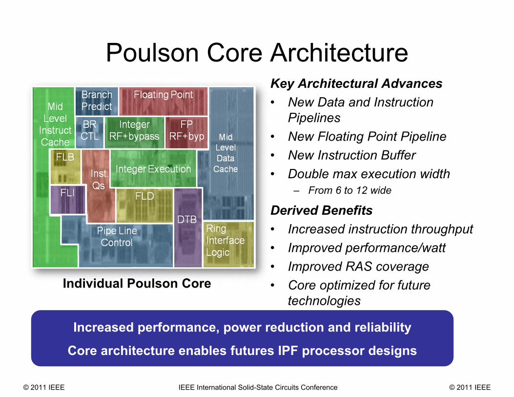
Poulson Core ArchitectureKey Architectural Advances• New Data and Instruction
Pipelines• New Floating Point Pipeline• New Instruction Buffer• Double max execution width
– From 6 to 12 wide
Derived Benefits• Increased instruction throughput• Improved performance/watt• Improved RAS coverage• Core optimized for future
technologies
Increased performance, power reduction and reliability
Core architecture enables futures IPF processor designs
Individual Poulson Core
© 2011 IEEE IEEE International Solid-State Circuits Conference © 2011 IEEE
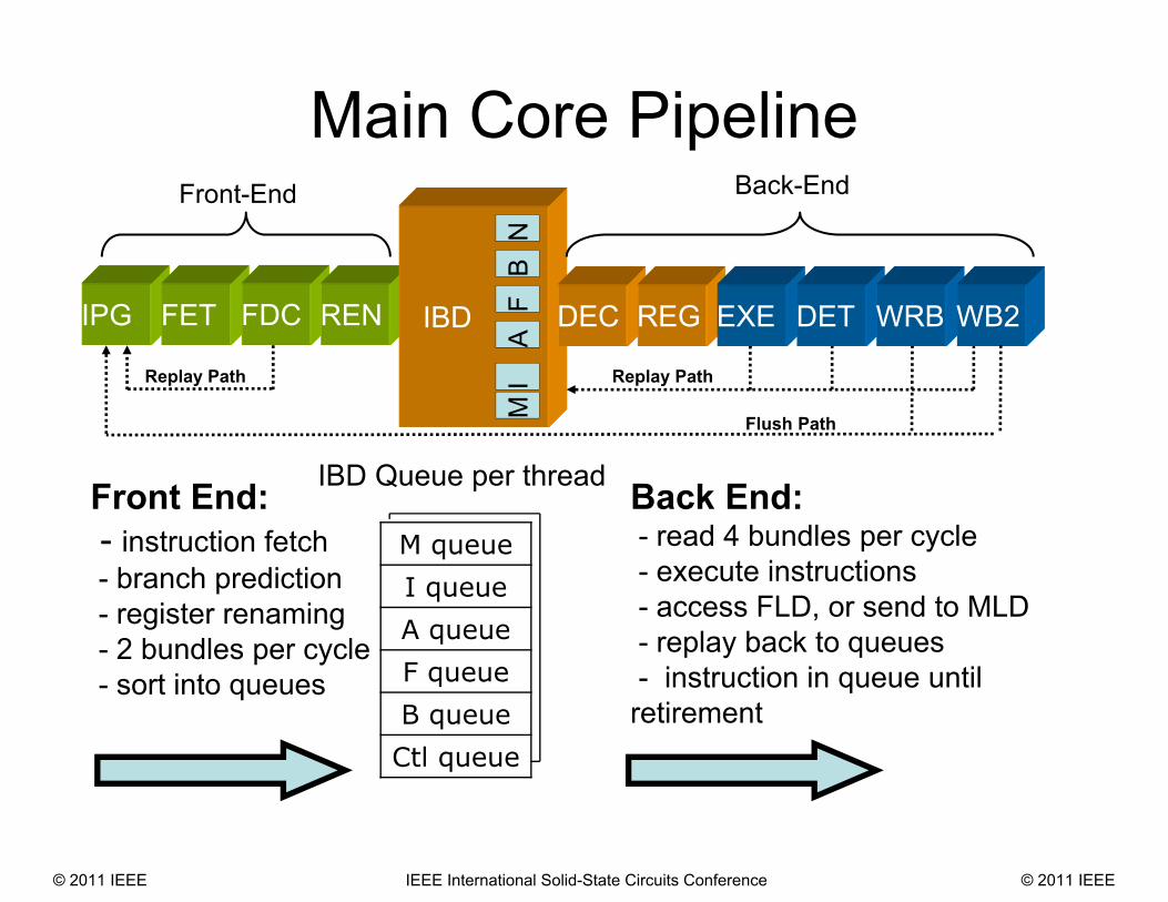
IPG FET FDC REN
Main Core Pipeline
IBD
MI
AF
BN
Back-EndFront-End
Flush Path
Replay PathReplay Path
DEC REG EXE DET WRB WB2
IBD Queue per thread
M queueI queueA queueF queueB queueCtl queue
Front End:- instruction fetch- branch prediction- register renaming- 2 bundles per cycle- sort into queues
Back End:- read 4 bundles per cycle- execute instructions- access FLD, or send to MLD- replay back to queues- instruction in queue until retirement
© 2011 IEEE IEEE International Solid-State Circuits Conference © 2011 IEEE
9
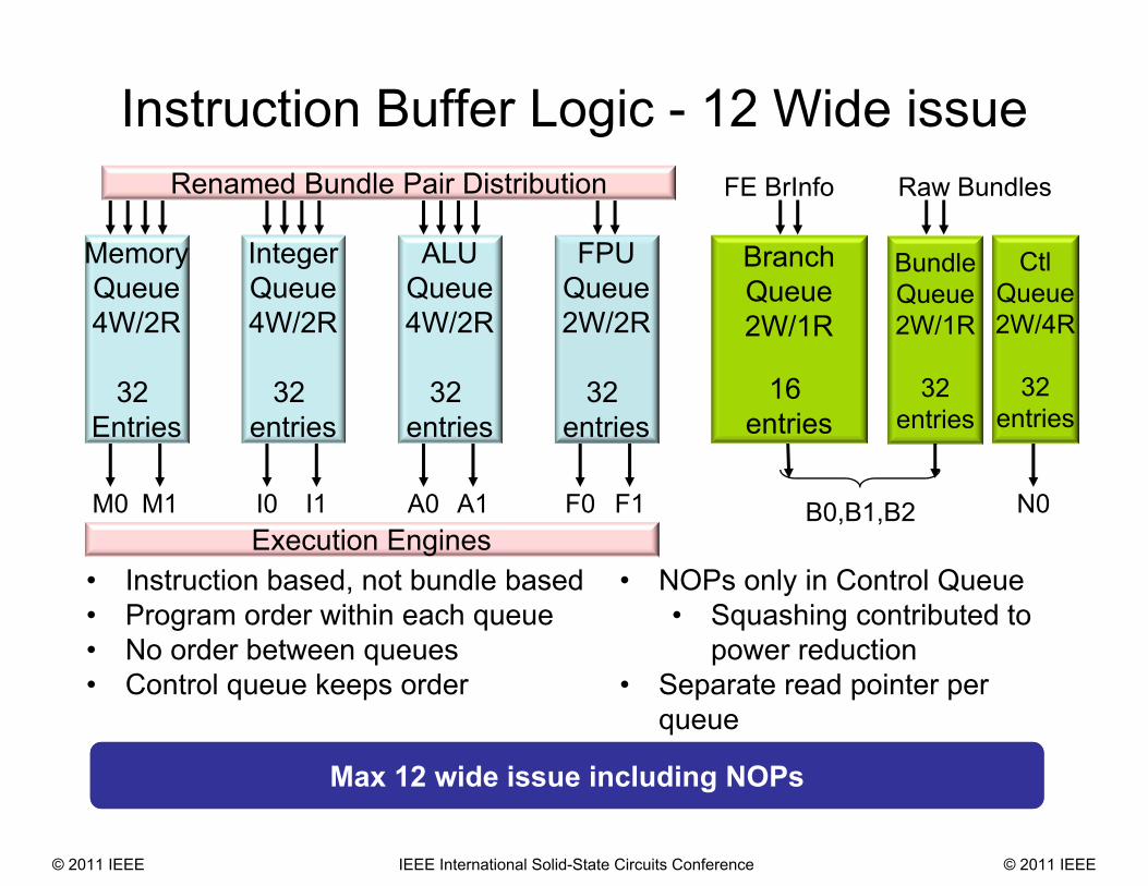
Instruction Buffer Logic - 12 Wide issue
MemoryQueue4W/2R
32 Entries
IntegerQueue4W/2R
32 entries
FPUQueue2W/2R
32 entries
ALUQueue4W/2R
32 entries
BranchQueue2W/1R
16 entries
M0 M1 I0 I1 A0 A1 F0 F1 B0,B1,B2
BundleQueue2W/1R
32entries
Execution Engines
FE BrInfo Raw Bundles
• Instruction based, not bundle based• Program order within each queue• No order between queues • Control queue keeps order
Renamed Bundle Pair Distribution
• NOPs only in Control Queue• Squashing contributed to
power reduction• Separate read pointer per
queue
Max 12 wide issue including NOPs
CtlQueue2W/4R
32entries
N0
© 2011 IEEE IEEE International Solid-State Circuits Conference © 2011 IEEE
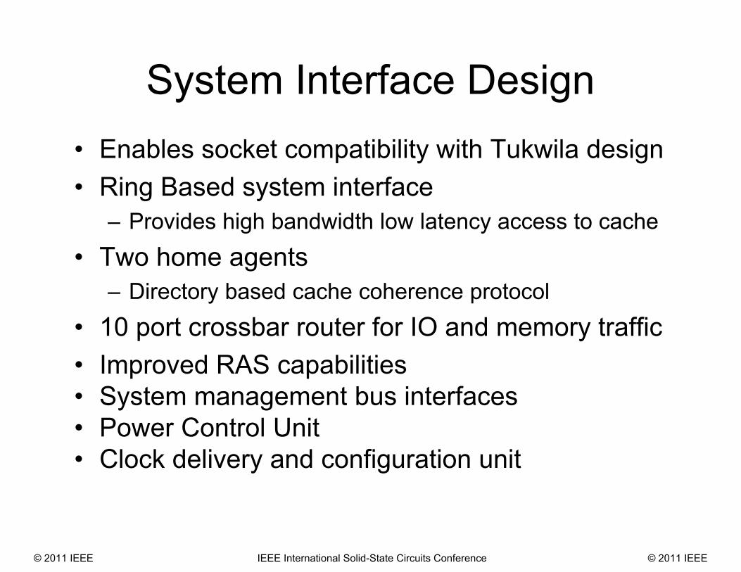
System Interface Design• Enables socket compatibility with Tukwila design• Ring Based system interface
– Provides high bandwidth low latency access to cache • Two home agents
– Directory based cache coherence protocol• 10 port crossbar router for IO and memory traffic• Improved RAS capabilities• System management bus interfaces• Power Control Unit • Clock delivery and configuration unit
© 2011 IEEE IEEE International Solid-State Circuits Conference © 2011 IEEE
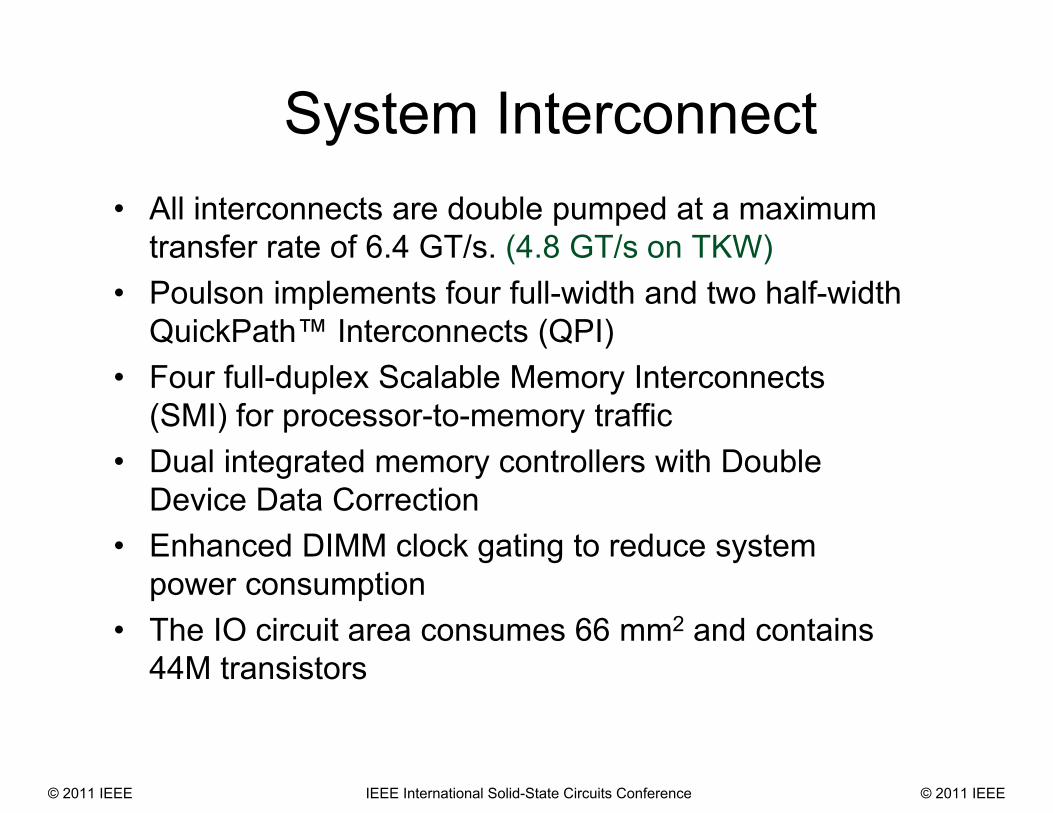
System Interconnect• All interconnects are double pumped at a maximum
transfer rate of 6.4 GT/s. (4.8 GT/s on TKW)• Poulson implements four full-width and two half-width
QuickPath™ Interconnects (QPI)• Four full-duplex Scalable Memory Interconnects
(SMI) for processor-to-memory traffic• Dual integrated memory controllers with Double
Device Data Correction• Enhanced DIMM clock gating to reduce system
power consumption• The IO circuit area consumes 66 mm2 and contains
44M transistors
© 2011 IEEE IEEE International Solid-State Circuits Conference © 2011 IEEE
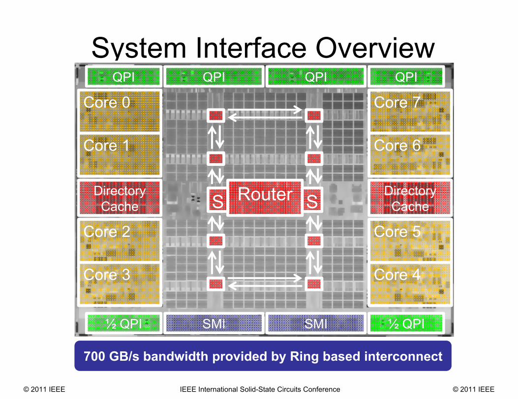
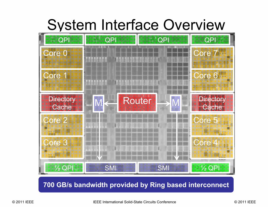
System Interface Overview
Core 0
Directory Cache
Directory Cache
Router
QPI QPIQPI QPI
SMI SMI ½ QPI½ QPI
Core 1
Core 2
Core 3 Core 4
Core 5
Core 7
Core 6
700 GB/s bandwidth provided by Ring based interconnect
S S
© 2011 IEEE IEEE International Solid-State Circuits Conference © 2011 IEEE
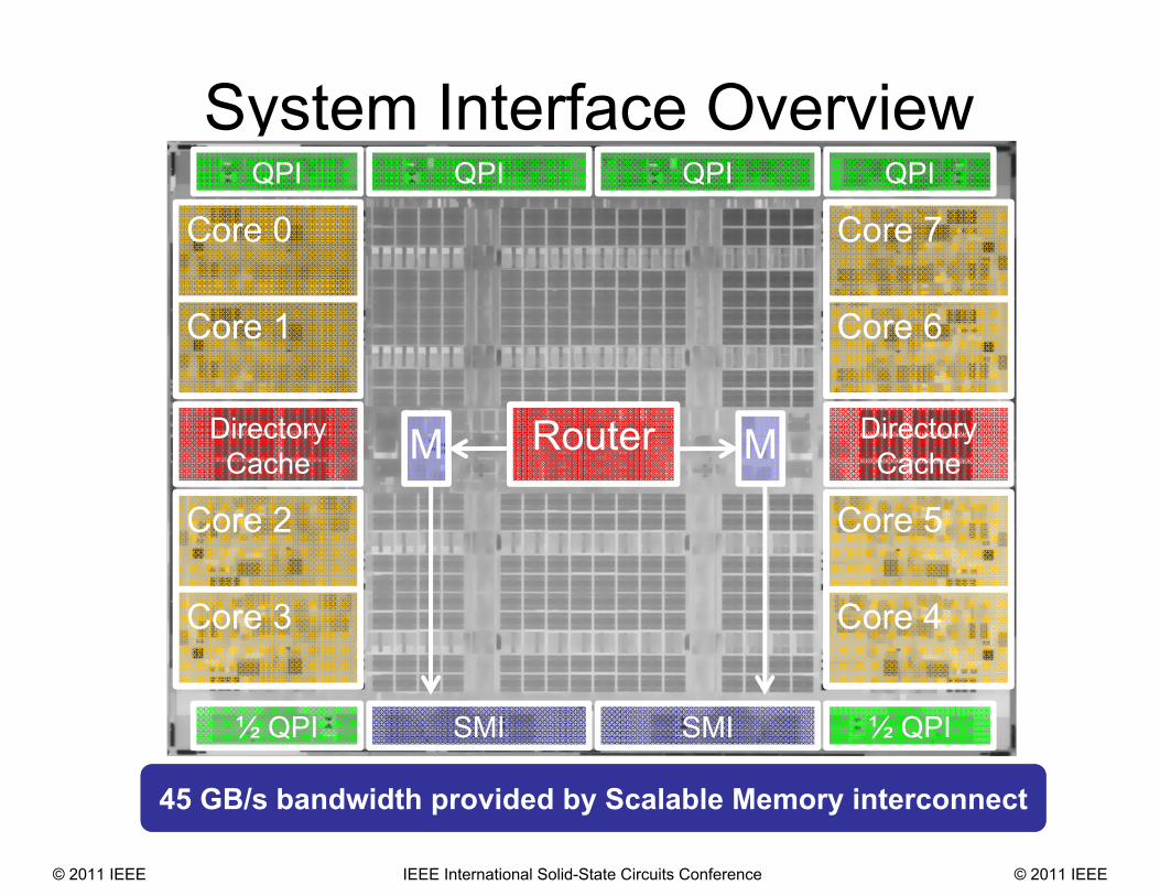
System Interface Overview
Core 0
Directory Cache
Directory Cache
Router
QPI QPIQPI QPI
SMI SMI ½ QPI½ QPI
Core 1
Core 2
Core 3 Core 4
Core 5
Core 7
Core 6
M M
45 GB/s bandwidth provided by Scalable Memory interconnect
© 2011 IEEE IEEE International Solid-State Circuits Conference © 2011 IEEE
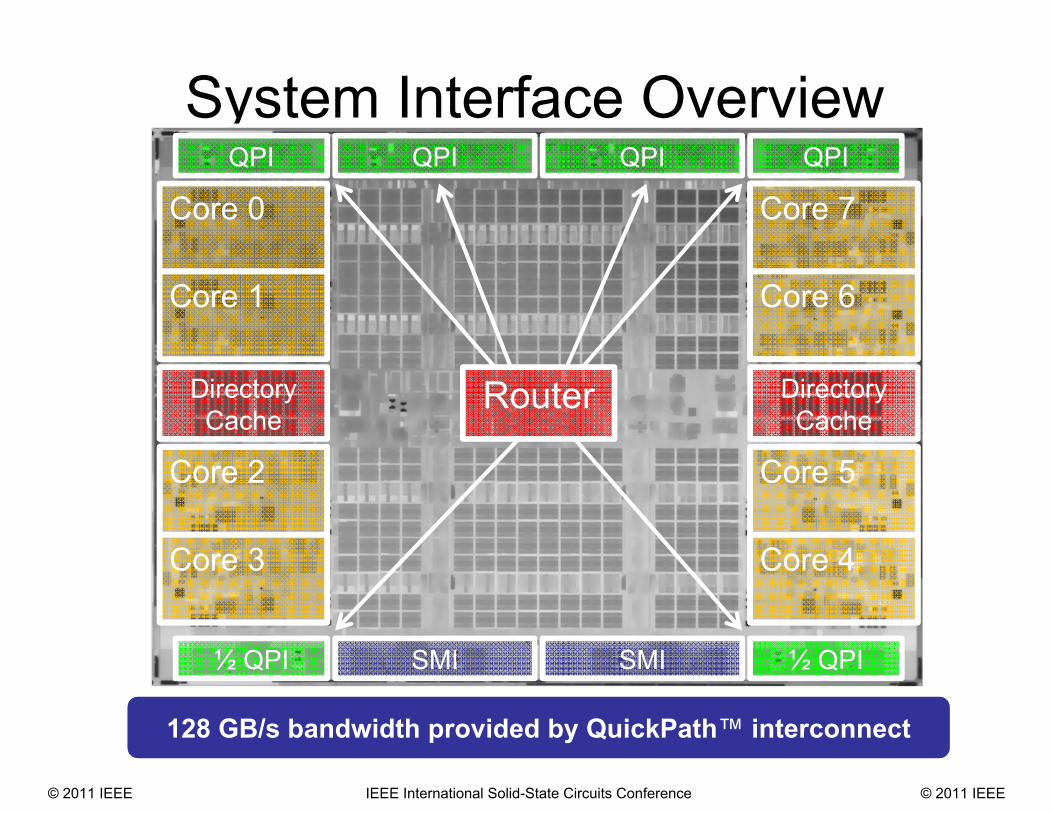
System Interface Overview
Core 0
Directory Cache
Directory Cache
Router
QPI QPIQPI QPI
SMI SMI ½ QPI½ QPI
Core 1
Core 2
Core 3 Core 4
Core 5
Core 7
Core 6
128 GB/s bandwidth provided by QuickPath™ interconnect
© 2011 IEEE IEEE International Solid-State Circuits Conference © 2011 IEEE
System Interface Overview
Core 0
Directory Cache
Directory Cache
Router
QPI QPIQPI QPI
SMI SMI ½ QPI½ QPI
Core 1
Core 2
Core 3 Core 4
Core 5
Core 7
Core 6
700 GB/s bandwidth provided by Ring based interconnect
M M
© 2011 IEEE IEEE International Solid-State Circuits Conference © 2011 IEEE
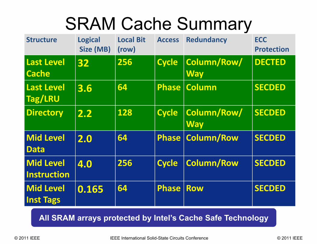
SRAM Cache SummaryStructure Logical
Size (MB)Local Bit(row)
Access Redundancy ECCProtection
Last Level Cache
32 256 Cycle Column/Row/Way
DECTED
Last LevelTag/LRU
3.6 64 Phase Column SECDED
Directory 2.2 128 Cycle Column/Row/Way
SECDED
Mid LevelData
2.0 64 Phase Column/Row SECDED
Mid Level Instruction
4.0 256 Cycle Column/Row SECDED
Mid Level Inst Tags
0.165 64 Phase Row SECDED
All SRAM arrays protected by Intel’s Cache Safe Technology
© 2011 IEEE IEEE International Solid-State Circuits Conference © 2011 IEEE
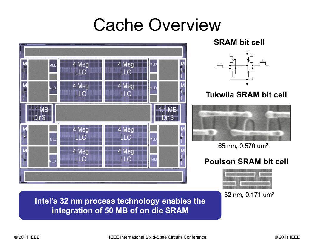
Cache Overview
Intel’s 32 nm process technology enables the integration of 50 MB of on die SRAM
65 nm, 0.570 um265 nm, 0.570 um2
32 nm, 0.171 um232 nm, 0.171 um2
Poulson SRAM bit cell
Tukwila SRAM bit cell
SRAM bit cell
© 2011 IEEE IEEE International Solid-State Circuits Conference © 2011 IEEE
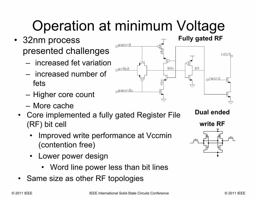
Operation at minimum Voltage• 32nm process
presented challenges– increased fet variation– increased number of
fets– Higher core count– More cache
Fully gated RF
• Core implemented a fully gated Register File (RF) bit cell• Improved write performance at Vccmin
(contention free)• Lower power design
• Word line power less than bit lines• Same size as other RF topologies
Dual ended
write RF
© 2011 IEEE IEEE International Solid-State Circuits Conference © 2011 IEEE
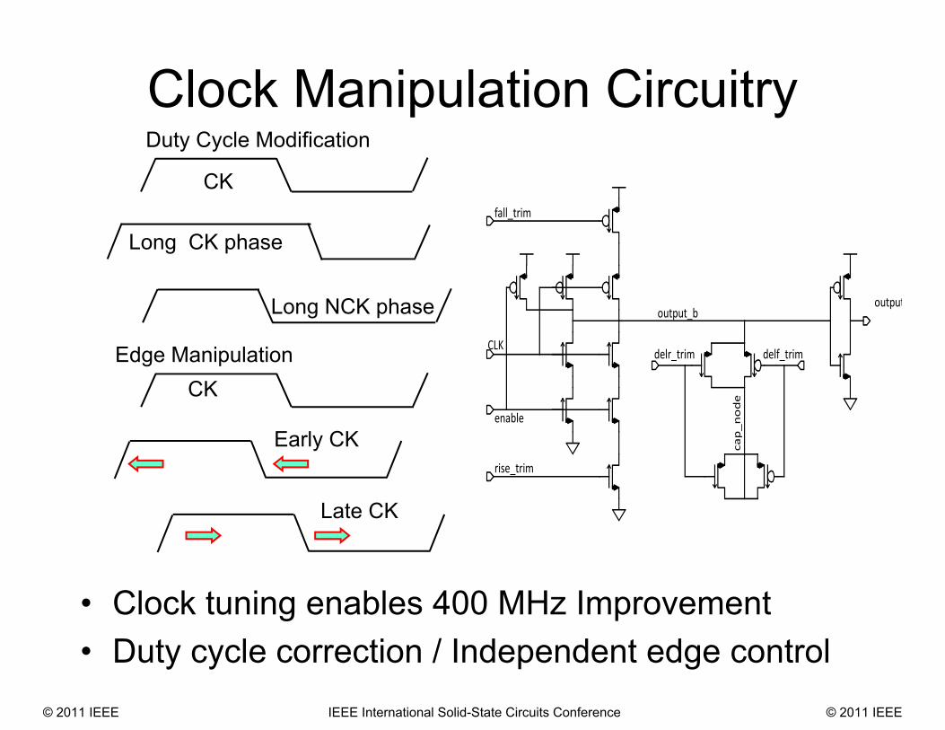
output
fall_trim
CLK
enable
rise_trim
delr_trim delf_trim
output_b
cap_node
Clock Manipulation Circuitry
• Clock tuning enables 400 MHz Improvement • Duty cycle correction / Independent edge control
CK
CK
Early CK
Late CK
Duty Cycle Modification
Edge Manipulation
Long NCK phase
Long CK phase
© 2011 IEEE IEEE International Solid-State Circuits Conference © 2011 IEEE
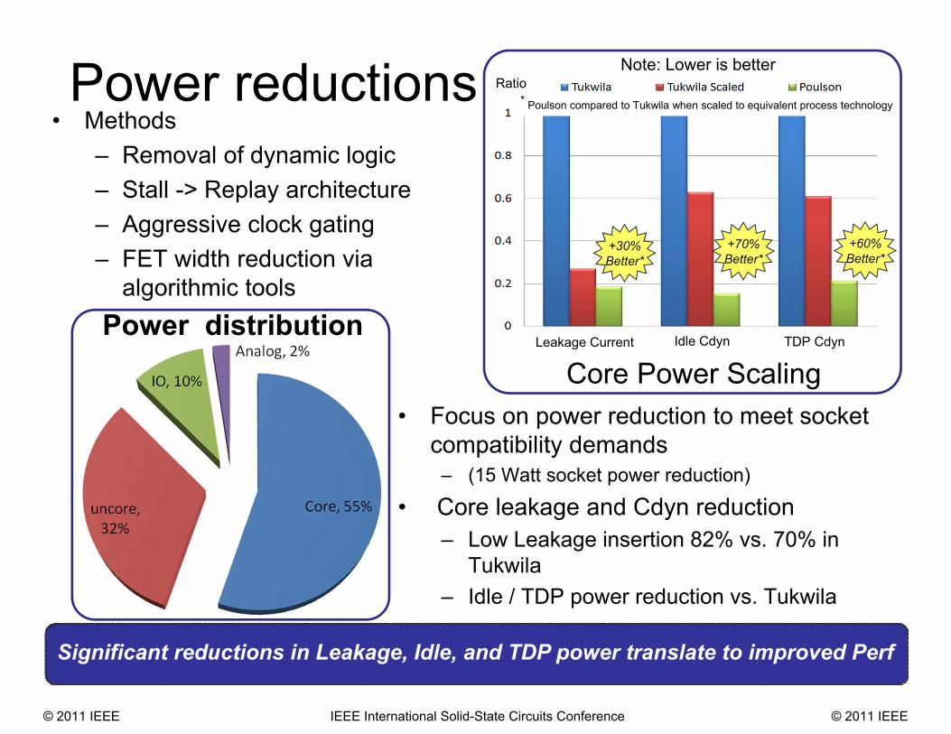
Power reductions
• Focus on power reduction to meet socket compatibility demands
– (15 Watt socket power reduction)
• Core leakage and Cdyn reduction– Low Leakage insertion 82% vs. 70% in
Tukwila– Idle / TDP power reduction vs. Tukwila
ww07'09Significant reductions in Leakage, Idle, and TDP power translate to improved Perf
Power distribution
• Methods– Removal of dynamic logic– Stall -> Replay architecture– Aggressive clock gating– FET width reduction via
algorithmic tools
Note: Lower is better
+70%Better*
+60%Better*
+30%Better*
Leakage Current Idle Cdyn TDP Cdyn
Ratio* Poulson compared to Tukwila when scaled to equivalent process technology
Core Power Scaling
© 2011 IEEE IEEE International Solid-State Circuits Conference © 2011 IEEE
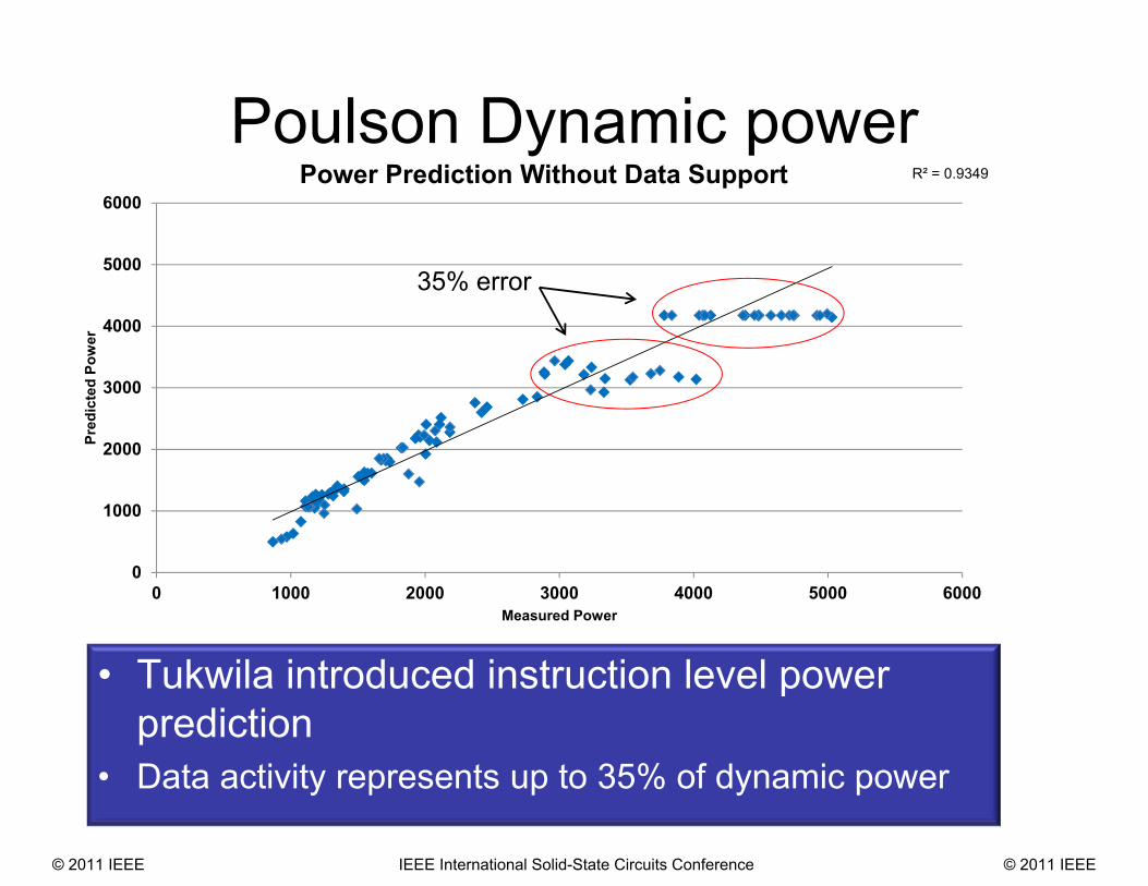
R² = 0.9349
0
1000
2000
3000
4000
5000
6000
0 1000 2000 3000 4000 5000 6000
Pred
icte
d Po
wer
Measured Power
Power Prediction Without Data Support
35% error
Poulson Dynamic power
• Tukwila introduced instruction level power prediction
• Data activity represents up to 35% of dynamic power
© 2011 IEEE IEEE International Solid-State Circuits Conference © 2011 IEEE
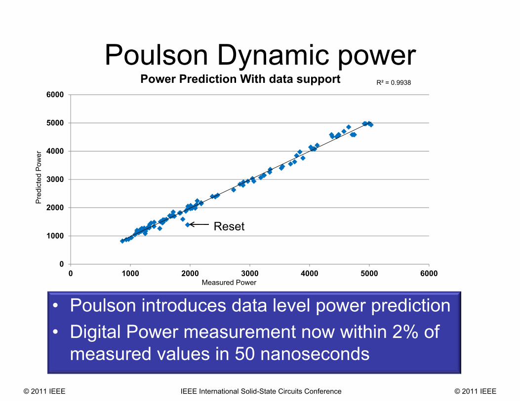
Poulson Dynamic powerR² = 0.9938
0
1000
2000
3000
4000
5000
6000
0 1000 2000 3000 4000 5000 6000
Power Prediction With data support
Pre
dict
ed P
ower
Measured Power
Reset
• Poulson introduces data level power prediction• Digital Power measurement now within 2% of
measured values in 50 nanoseconds
© 2011 IEEE IEEE International Solid-State Circuits Conference © 2011 IEEE
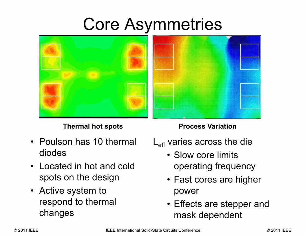
Core Asymmetries
• Poulson has 10 thermal diodes
• Located in hot and cold spots on the design
• Active system to respond to thermal changes
Thermal hot spots Process Variation
Leff varies across the die • Slow core limits
operating frequency• Fast cores are higher
power • Effects are stepper and
mask dependent© 2011 IEEE IEEE International Solid-State Circuits Conference © 2011 IEEE
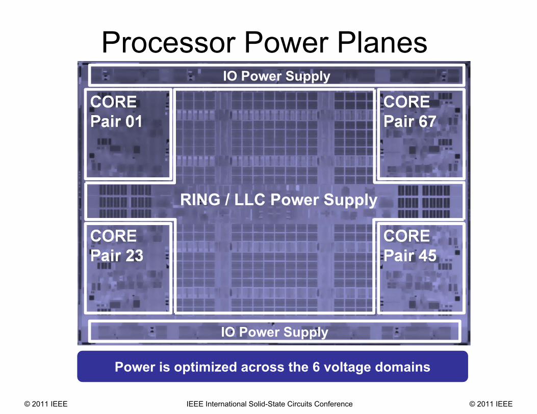
Processor Power Planes
CORE Pair 01
IO Power Supply
IO Power Supply
CORE Pair 23
CORE Pair 45
CORE Pair 67
RING / LLC Power Supply
Power is optimized across the 6 voltage domains
© 2011 IEEE IEEE International Solid-State Circuits Conference © 2011 IEEE
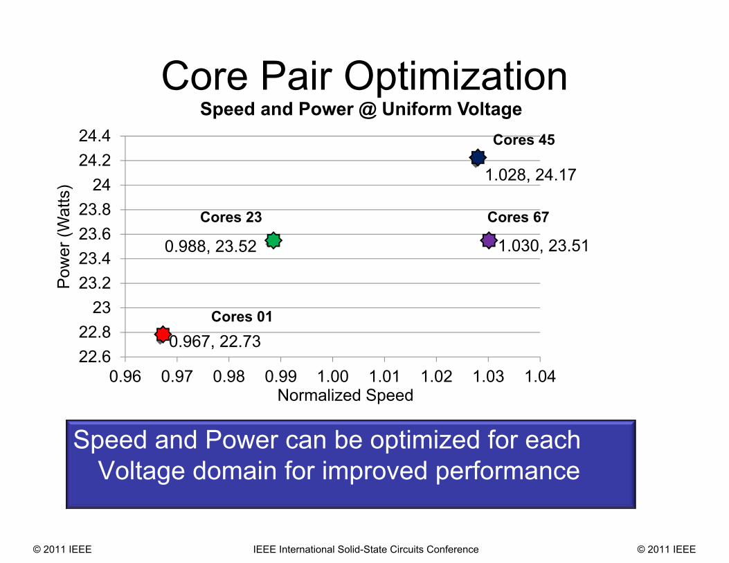
0.967, 22.73
0.988, 23.52
1.028, 24.17
1.030, 23.51
22.622.8
2323.223.423.623.8
2424.224.4
0.96 0.97 0.98 0.99 1.00 1.01 1.02 1.03 1.04
Cores 01
Cores 45
Cores 23 Cores 67
Core Pair Optimization
Speed and Power can be optimized for each Voltage domain for improved performance
Speed and Power @ Uniform Voltage
Pow
er (W
atts
)
Normalized Speed
© 2011 IEEE IEEE International Solid-State Circuits Conference © 2011 IEEE
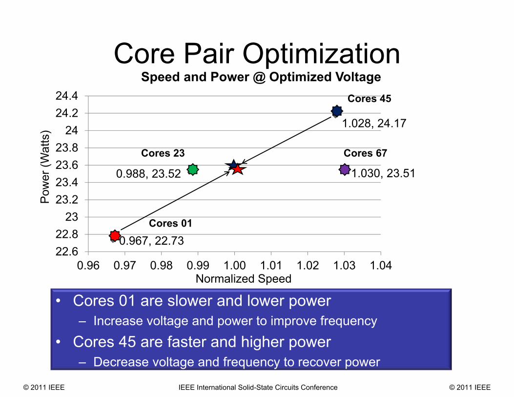
Speed and Power @ Optimized Voltage
0.967, 22.73
0.988, 23.52
1.028, 24.17
1.030, 23.51
22.622.8
2323.223.423.623.8
2424.224.4
0.96 0.97 0.98 0.99 1.00 1.01 1.02 1.03 1.04
Cores 01
Cores 45
Cores 23 Cores 67
Core Pair Optimization
• Cores 01 are slower and lower power– Increase voltage and power to improve frequency
• Cores 45 are faster and higher power– Decrease voltage and frequency to recover power
Pow
er (W
atts
)
Normalized Speed
© 2011 IEEE IEEE International Solid-State Circuits Conference © 2011 IEEE
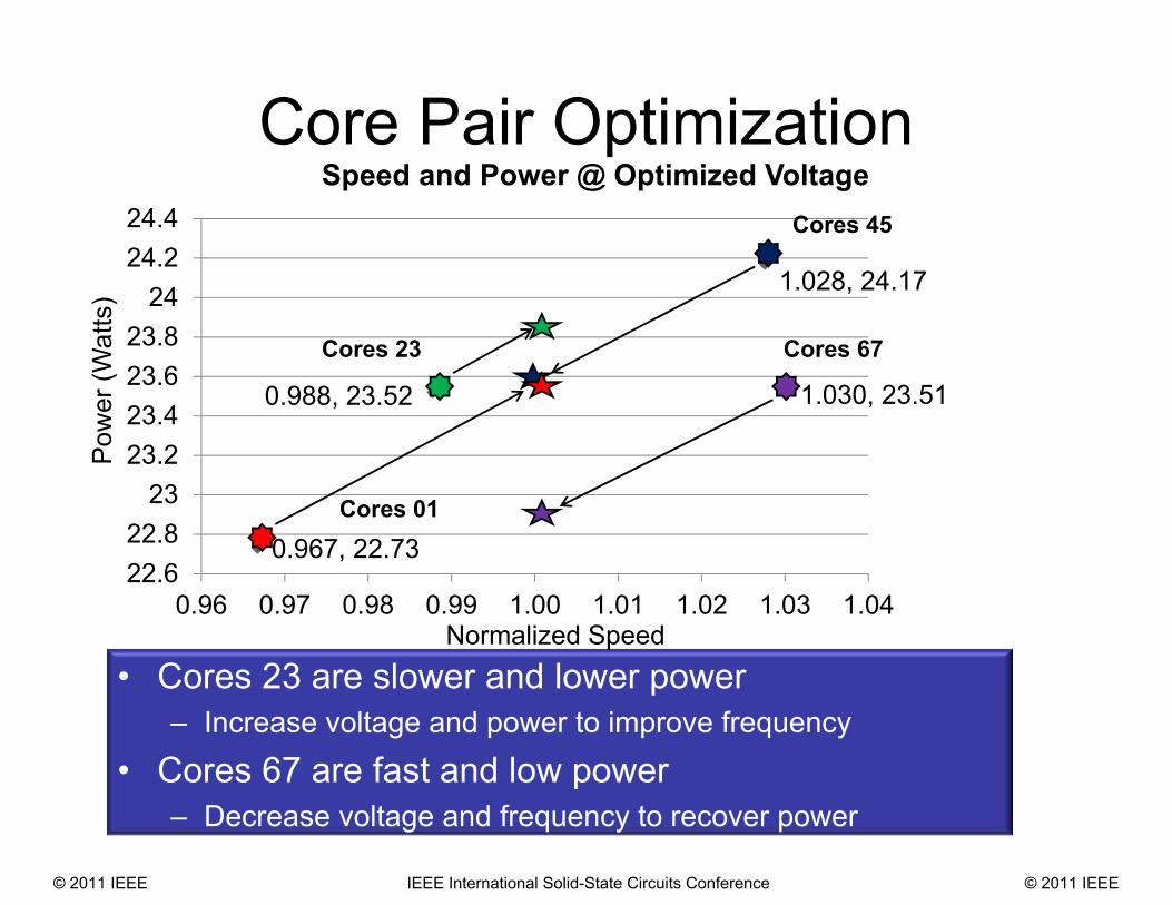
Speed and Power @ Optimized Voltage
0.967, 22.73
0.988, 23.52
1.028, 24.17
1.030, 23.51
22.622.8
2323.223.423.623.8
2424.224.4
0.96 0.97 0.98 0.99 1.00 1.01 1.02 1.03 1.04
Cores 01
Cores 45
Cores 23 Cores 67
Core Pair Optimization
• Cores 23 are slower and lower power– Increase voltage and power to improve frequency
• Cores 67 are fast and low power– Decrease voltage and frequency to recover power
Pow
er (W
atts
)
Normalized Speed
© 2011 IEEE IEEE International Solid-State Circuits Conference © 2011 IEEE
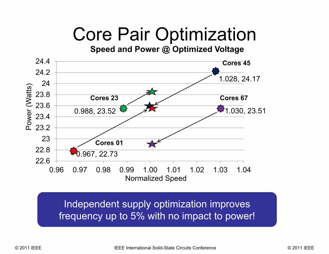
Speed and Power @ Optimized Voltage
0.967, 22.73
0.988, 23.52
1.028, 24.17
1.030, 23.51
22.622.8
2323.223.423.623.8
2424.224.4
0.96 0.97 0.98 0.99 1.00 1.01 1.02 1.03 1.04
Cores 01
Cores 45
Cores 23 Cores 67
Core Pair OptimizationP
ower
(Wat
ts)
Normalized Speed
Independent supply optimization improves frequency up to 5% with no impact to power!
© 2011 IEEE IEEE International Solid-State Circuits Conference © 2011 IEEE
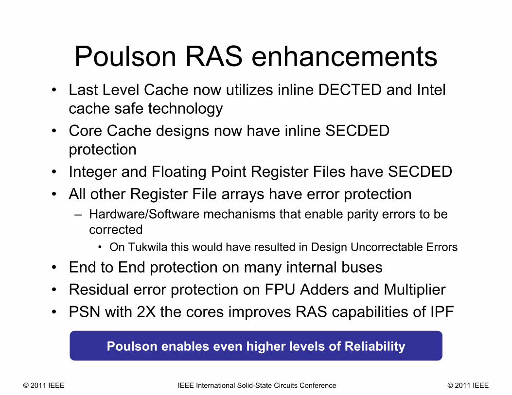
Poulson RAS enhancements• Last Level Cache now utilizes inline DECTED and Intel
cache safe technology• Core Cache designs now have inline SECDED
protection• Integer and Floating Point Register Files have SECDED• All other Register File arrays have error protection
– Hardware/Software mechanisms that enable parity errors to be corrected
• On Tukwila this would have resulted in Design Uncorrectable Errors
• End to End protection on many internal buses• Residual error protection on FPU Adders and Multiplier• PSN with 2X the cores improves RAS capabilities of IPF
Poulson enables even higher levels of Reliability
© 2011 IEEE IEEE International Solid-State Circuits Conference © 2011 IEEE
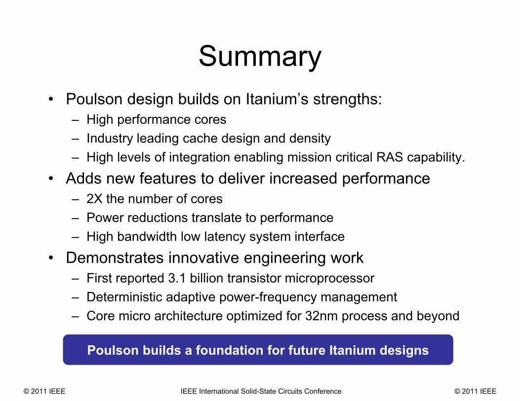
Summary• Poulson design builds on Itanium’s strengths:
– High performance cores– Industry leading cache design and density– High levels of integration enabling mission critical RAS capability.
• Adds new features to deliver increased performance– 2X the number of cores– Power reductions translate to performance– High bandwidth low latency system interface
• Demonstrates innovative engineering work– First reported 3.1 billion transistor microprocessor – Deterministic adaptive power-frequency management– Core micro architecture optimized for 32nm process and beyond
Poulson builds a foundation for future Itanium designs
© 2011 IEEE IEEE International Solid-State Circuits Conference © 2011 IEEE