
8279nptel
39
M. Krishna Kumar MM/M3/LU9c/V1/2004 1 8279 • While studying 8255, we have explained the use of 8255 in interfacing keyboards and displays with 8086. The disadvantages of this method of interfacing keyboard and display with 8086 is that the processor has to refresh the display and check the status of the keyboard periodically using polling technique. Thus a considerable amount of CPU time is wasted, reducing the system operating speed. • Intel’s 8279 is a general purpose keyboard display controller that simultaneously drives the display of a system and interfaces a keyboard with the CPU, leaving it free for its routine task.
-
Upload
jemimajerome -
Category
Education
-
view
103 -
download
0
Transcript of 8279nptel

M. Krishna Kumar MM/M3/LU9c/V1/2004 1
8279• While studying 8255, we have explained the use of 8255 in
interfacing keyboards and displays with 8086. The disadvantages of this method of interfacing keyboard and display with 8086 is that the processor has to refresh the display and check the status of the keyboard periodically using polling technique. Thus a considerable amount of CPU time is wasted, reducing the system operating speed.
• Intel’s 8279 is a general purpose keyboard display controller that simultaneously drives the display of a system and interfaces a keyboard with the CPU, leaving it free for its routine task.
M. Krishna Kumar MM/M3/LU9c/V1/2004 2
• The keyboard display controller chip 8279 provides:a) a set of four scan lines and eight return lines for
interfacing keyboardsb) A set of eight output lines for interfacing display.• Fig shows the functional block diagram of 8279
followed by its brief description.• I/O Control and Data Buffers : The I/O control section
controls the flow of data to/from the 8279. The data buffers interface the external bus of the system with internal bus of 8279.
Architecture and Signal Descriptions of 8279 (cont..)

M. Krishna Kumar MM/M3/LU9c/V1/2004 3
• The I/O section is enabled only if CS is low. The pins A0, RD and WR select the command, status or data read/write operations carried out by the CPU with 8279.
• Control and Timing Register and Timing Control : These registers store the keyboard and display modes and other operating conditions programmed by CPU. The registers are written with A0=1 and WR=0. The Timing and control unit controls the basic timings for the operation of the circuit. Scan counter divide down the operating frequency of 8279 to derive scan keyboard and scan display frequencies.
Architecture and Signal Descriptions of 8279 (cont..)

M. Krishna Kumar MM/M3/LU9c/V1/2004 4
• Scan Counter : The scan counter has two modes to scan the key matrix and refresh the display. In the encoded mode, the counter provides binary count that is to be externally decoded to provide the scan lines for keyboard and display (Four externally decoded scan lines may drive upto 16 displays). In the decode scan mode, the counter internally decodes the least significant 2 bits and provides a decoded 1 out of 4 scan on SL0-SL3( Four internally decoded scan lines may drive upto 4 displays). The keyboard and display both are in the same mode at a time.
Architecture and Signal Descriptions of 8279 (cont..)

M. Krishna Kumar MM/M3/LU9c/V1/2004 5
• Return Buffers and Keyboard Debounce and Control: This section for a key closure row wise. If a key closer is detected, the keyboard debounce unit debounces the key entry (i.e. wait for 10 ms). After the debounce period, if the key continues to be detected. The code of key is directly transferred to the sensor RAM along with SHIFT and CONTROL key status.
• FIFO/Sensor RAM and Status Logic: In keyboard or strobed input mode, this block acts as 8-byte first-in-first-out (FIFO) RAM. Each key code of the pressed key is entered in the order of the entry and in the mean time read by the CPU, till the RAM become empty.
Architecture and Signal Descriptions of 8279 (cont..)

M. Krishna Kumar MM/M3/LU9c/V1/2004 6
• The status logic generates an interrupt after each FIFO read operation till the FIFO is empty. In scanned sensor matrix mode, this unit acts as sensor RAM. Each row of the sensor RAM is loaded with the status of the corresponding row of sensors in the matrix. If a sensor changes its state, the IRQ line goes high to interrupt the CPU.
• Display Address Registers and Display RAM : The display address register holds the address of the word currently being written or read by the CPU to or from the display RAM. The contents of the registers are automatically updated by 8279 to accept the next data entry by CPU.
Architecture and Signal Descriptions of 8279 (cont..)

M. Krishna Kumar MM/M3/LU9c/V1/2004 7
8279 Internal Architecture
Return
DB0-DB7
DATA BUFFERS
I/O CONTROL
INTERNAL 8 BIT DATA BUS
FIFO/SENSOR RAM STATUS
RD WR
DISPLAY ADDRESS REGISTERS
16*8 DISPLAY RAM
A0CS
CONTROL AND TIMING REGISTERS
8*8 FIFO/ SENSOR RAM
KEYBOARD DEBOUNCE AND CONTROL
DISPLAY REGISTERS
TIMING AND CONTROL UNIT
SCAN COUNTER
BDOUT A0-A3OUT B0-B3
SL0 – SL3RL0 – RL7 CNTL/
STB
SHIFT
CLK
RE
SET
M. Krishna Kumar MM/M3/LU9c/V1/2004 8
8279
1234567891011121314151617181920
4039383736353433323130292827262524232221
VccRL1RL0CNTL/STBSHIFTSL3SL2SL1SL0OUT B0OUT B1OUT B2OUT B3OUT A0OUT A1OUT A2OUT A3BDCSA0
RL2RL3
CLKIRQRL4RL5RL6RL7
RESETRDWRDB0DB1DB2DB3DB4DB5DB6DB7Vss
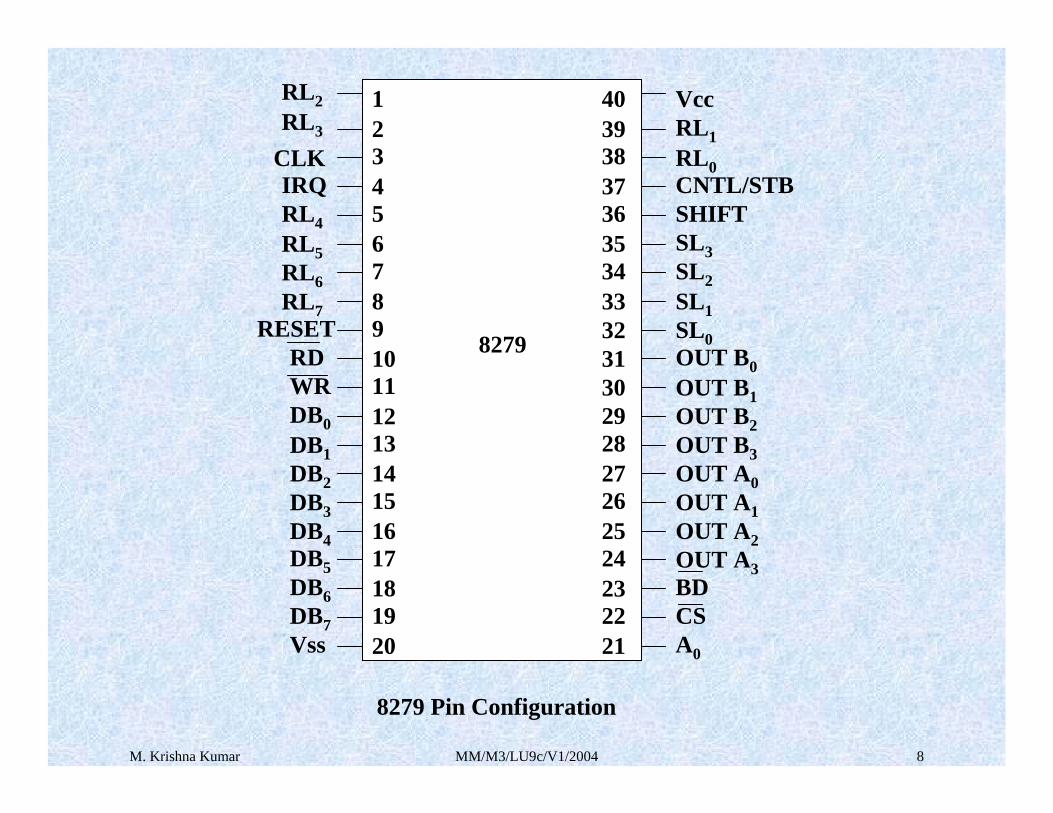
8279 Pin Configuration

M. Krishna Kumar MM/M3/LU9c/V1/2004 9
Vss
BD
4
KRY DATA
8RL0-7
SHIFT
CLK
RESET
A0
CS
WR
RD
DB0 – DB7
IRQ
8
CNTL/STB
SL0-3 4SCAN
OUT A0-A3
OUT B0 – B3
4
Vcc
DISPLAY DATA
CPU INTERFACE
8279

M. Krishna Kumar MM/M3/LU9c/V1/2004 10
• The signal discription of each of the pins of 8279 as follows :
• DB0-DB7 : These are bidirectional data bus lines. The data and command words to and from the CPU are transferred on these lines.
• CLK : This is a clock input used to generate internal timing required by 8279.
• RESET : This pin is used to reset 8279. A high on this line reset 8279. After resetting 8279, its in sixteen 8-bit display, left entry encoded scan, 2-key lock out mode. The clock prescaler is set to 31.
Architecture and Signal Descriptions of 8279 (cont..)
M. Krishna Kumar MM/M3/LU9c/V1/2004 11
• CS : Chip Select – A low on this line enables 8279 for normal read or write operations. Other wise, this pin should remain high.
• A0 : A high on this line indicates the transfer of a command or status information. A low on this line indicates the transfer of data. This is used to select one of the internal registers of 8279.
• RD, WR ( Input/Output ) READ/WRITE – These input pins enable the data buffers to receive or send data over the data bus.
Architecture and Signal Descriptions of 8279 (cont..)
M. Krishna Kumar MM/M3/LU9c/V1/2004 12
• IRQ : This interrupt output lines goes high when there is a data in the FIFO sensor RAM. The interrupt lines goes low with each FIFO RAM read operation but if the FIFO RAM further contains any key-code entry to be read by the CPU, this pin again goes high to generate an interrupt to the CPU.
• Vss, Vcc : These are the ground and power supply lines for the circuit.
• SL0-SL3-Scan Lines : These lines are used to scan the key board matrix and display digits. These lines can be programmed as encoded or decoded, using the mode control register.
Architecture and Signal Descriptions of 8279 (cont..)

M. Krishna Kumar MM/M3/LU9c/V1/2004 13
• RL0 - RL7 - Return Lines : These are the input lines which are connected to one terminal of keys, while the other terminal of the keys are connected to the decoded scan lines. These are normally high, but pulled low when a key is pressed.
• SHIFT : The status of the shift input lines is stored along with each key code in FIFO, in scanned keyboard mode. It is pulled up internally to keep it high, till it is pulled low with a key closure.
• BD – Blank Display : This output pin is used to blank the display during digit switching or by a blanking closure.
Architecture and Signal Descriptions of 8279 (cont..)
M. Krishna Kumar MM/M3/LU9c/V1/2004 14
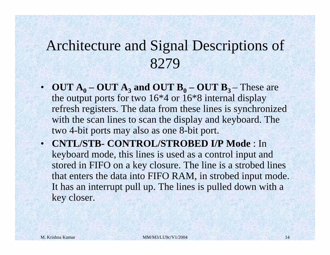
• OUT A0 – OUT A3 and OUT B0 – OUT B3 – These are the output ports for two 16*4 or 16*8 internal display refresh registers. The data from these lines is synchronized with the scan lines to scan the display and keyboard. The two 4-bit ports may also as one 8-bit port.
• CNTL/STB- CONTROL/STROBED I/P Mode : In keyboard mode, this lines is used as a control input and stored in FIFO on a key closure. The line is a strobed lines that enters the data into FIFO RAM, in strobed input mode. It has an interrupt pull up. The lines is pulled down with a key closer.
Architecture and Signal Descriptions of 8279
M. Krishna Kumar MM/M3/LU9c/V1/2004 15
Modes of Operation of 8279 (cont..)
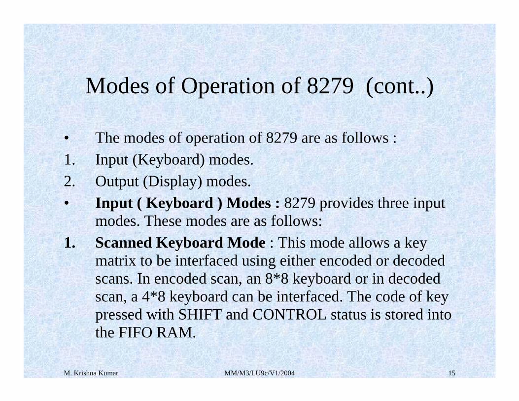
• The modes of operation of 8279 are as follows :1. Input (Keyboard) modes.2. Output (Display) modes.• Input ( Keyboard ) Modes : 8279 provides three input
modes. These modes are as follows:1. Scanned Keyboard Mode : This mode allows a key
matrix to be interfaced using either encoded or decoded scans. In encoded scan, an 8*8 keyboard or in decoded scan, a 4*8 keyboard can be interfaced. The code of key pressed with SHIFT and CONTROL status is stored into the FIFO RAM.

M. Krishna Kumar MM/M3/LU9c/V1/2004 16
2. Scanned Sensor Matrix : In this mode, a sensor array can be interfaced with 8279 using either encoded or decoded scans. With encoded scan 8*8 sensor matrix or with decoded scan 4*8 sensor matrix can be interfaced. The sensor codes are stored in the CPU addressable sensor RAM.
3. Strobed input: In this mode, if the control lines goes low, the data on return lines, is stored in the FIFO byte by byte.
Modes of Operation of 8279 (cont..)
M. Krishna Kumar MM/M3/LU9c/V1/2004 17
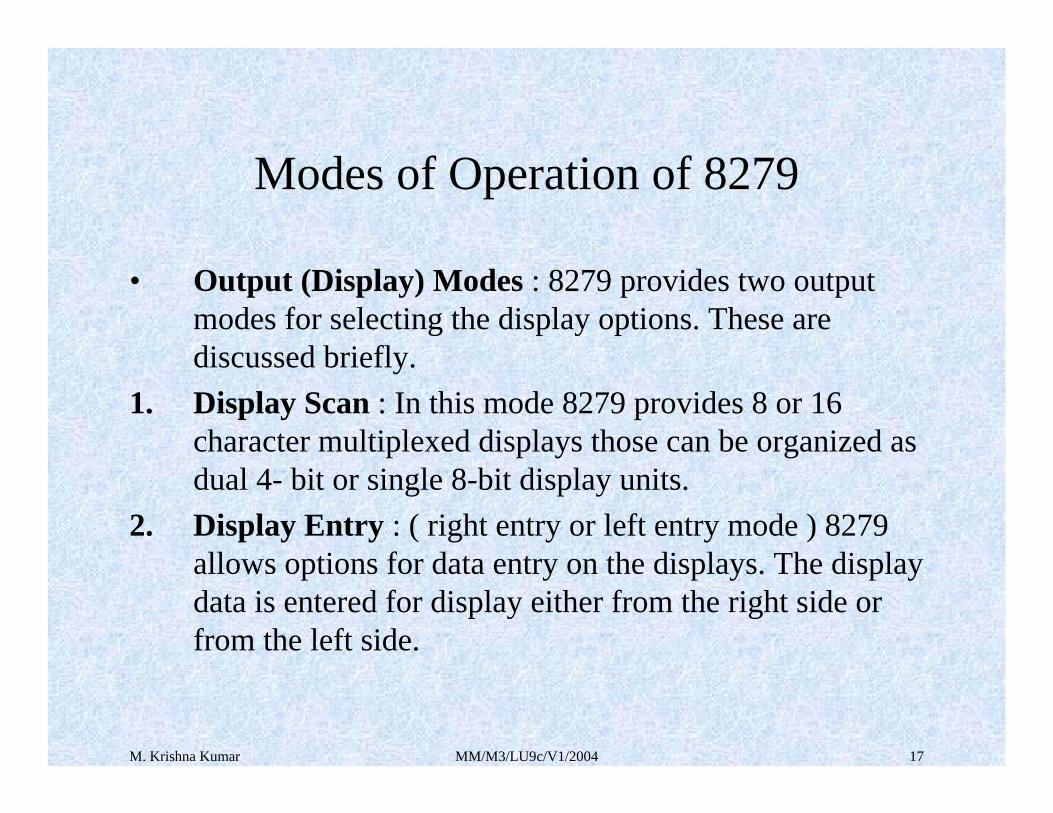
• Output (Display) Modes : 8279 provides two output modes for selecting the display options. These are discussed briefly.
1. Display Scan : In this mode 8279 provides 8 or 16 character multiplexed displays those can be organized as dual 4- bit or single 8-bit display units.
2. Display Entry : ( right entry or left entry mode ) 8279 allows options for data entry on the displays. The display data is entered for display either from the right side or from the left side.
Modes of Operation of 8279

M. Krishna Kumar MM/M3/LU9c/V1/2004 18
Keyboard Modes (cont..)
i. Scanned Keyboard mode with 2 Key Lockout : In this mode of operation, when a key is pressed, a debounce logic comes into operation. During the next two scans, other keys are checked for closure and if no other key is pressed the first pressed key is identified.
• The key code of the identified key is entered into the FIFO with SHIFT and CNTL status, provided the FIFO is not full, i.e. it has at least one byte free. If the FIFO does not have any free byte, naturally the key data will not be entered and the error flag is set.

M. Krishna Kumar MM/M3/LU9c/V1/2004 19
• If FIFO has at least one byte free, the above code is entered into it and the 8279 generates an interrupt on IRQ line to the CPU to inform about the previous key closures. If another key is found closed during the first key, the keycode is entered in FIFO.
• If the first pressed key is released before the others, the first will be ignored. A key code is entered to FIFO only once for each valid depression, independent of other keys pressed along with it, or released before it.
Keyboard Modes (cont..)

M. Krishna Kumar MM/M3/LU9c/V1/2004 20
• If two keys are pressed within a debounce cycle (simultaneously ), no key is recognized till one of them remains closed and the other is released. The last key, that remains depressed is considered as single valid key depression.
ii. Scanned Keyboard with N-Key Rollover : In this mode, each key depression is treated independently. When a key is pressed, the debounce circuit waits for 2 keyboards scans and then checks whether the key is still depressed. If it is still depressed, the code is entered in FIFO RAM.
Keyboard Modes (cont..)
M. Krishna Kumar MM/M3/LU9c/V1/2004 21
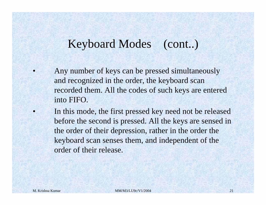
• Any number of keys can be pressed simultaneously and recognized in the order, the keyboard scan recorded them. All the codes of such keys are entered into FIFO.
• In this mode, the first pressed key need not be released before the second is pressed. All the keys are sensed in the order of their depression, rather in the order the keyboard scan senses them, and independent of the order of their release.
Keyboard Modes (cont..)

M. Krishna Kumar MM/M3/LU9c/V1/2004 22
iii. Scanned Keyboard Special Error Mode : This mode is valid only under the N-Key rollover mode. This mode is programmed using end interrupt / error mode set command. If during a single debounce period ( two keyboard scans ) two keys are found pressed , this is considered a simultaneous depression and an error flag is set.
• This flag, if set, prevents further writing in FIFO but allows the generation of further interrupts to the CPU for FIFO read. The error flag can be read by reading the FIFO status word. The error Flag is set by sending normal clear command with CF = 1.
Keyboard Modes (cont..)

M. Krishna Kumar MM/M3/LU9c/V1/2004 23
iv. Sensor Matrix Mode : In the sensor matrix mode, the debounce logic is inhibited. The 8-byte FIFO RAM now acts as 8 * 8 bit memory matrix. The status of the sensor switch matrix is fed directly to sensor RAM matrix. Thus the sensor RAM bits contains the row-wise and column wise status of the sensors in the sensor matrix.
• The IRQ line goes high, if any change in sensor value is detected at the end of a sensor matrix scan or the sensor RAM has a previous entry to be read by the CPU. The IRQ line is reset by the first data read operation, if AI = 0, otherwise, by issuing the end interrupt command. AI is a bit in read sensor RAM word.
Keyboard Modes.

M. Krishna Kumar MM/M3/LU9c/V1/2004 24
• There are various options of data display. For example, the command number of characters can be 8 or 16, with each character organised as single 8-bit or dual 4-bit codes. Similarly there are two display formats.
• The first one is known as left entry mode or type writer mode, since in a type writer the first character typed appears at the left-most position, while the subsequent characters appear successively to the right of the first one. The other display format is known as right entry mode, or calculator mode, since in a calculator the first character entered appears at the rightmost position and this character is shifted one position left when the next characters is entered.
Display Modes (cont..)

M. Krishna Kumar MM/M3/LU9c/V1/2004 25
• Thus all the previously entered characters are shifted left by one position when a new characters is entered.
i. Left Entry Mode : In the left entry mode, the data is entered from left side of the display unit. Address 0 of the display RAM contains the leftmost display characters and address 15 of the RAM contains the right most display characters. It is just like writing in our address is automatically updated with successive reads or writes. The first entry is displayed on the leftmost display and the sixteenth entry on the rightmost display. The seventeenth entry is again displayed at the leftmost display position.
Display Modes (cont..)
M. Krishna Kumar MM/M3/LU9c/V1/2004 26
ii. Right Entry Mode : In this right entry mode, the first entry to be displayed is entered on the rightmost display. The next entry is also placed in the right most display but after the previous display is shifted left by one display position. The leftmost characters is shifted out of that display at the seventeenth entry and is lost, i.e. it is pushed out of the display RAM.
Display Modes

M. Krishna Kumar MM/M3/LU9c/V1/2004 27
Command Words of 8279 (cont..)
• All the command words or status words are written or read with A0 = 1 and CS = 0 to or from 8279. This section describes the various command available in 8279.
a) Keyboard Display Mode Set – The format of the command word to select different modes of operation of 8279 is given below with its bit definitions.
D7 D6 D5 D4 D3 D2 D1 A0D00 0 D D D K K 1K

M. Krishna Kumar MM/M3/LU9c/V1/2004 28
D D Display modes
K K K Keyboard modes
0 0
0 1
1 0
1 1
Eight 8-bit character Left entrySixteen 8-bit character left entry
Eight 8-bit character Right entry
Sixteen 8-bit character Right entry
0 0 0 Encoded Scan, 2 key lockout ( Default after reset )0 0 10 1 0
0 1 11 0 0
1 0 1
1 1 0
1 1 1
Decoded Scan, 2 key lockoutEncoded Scan, N- key Roll overDecoded Scan, N- key Roll overEncode Scan, N- key Roll overDecoded Scan, N- key Roll over
Strobed Input Encoded ScanStrobed Input Decoded Scan
Fig:

M. Krishna Kumar MM/M3/LU9c/V1/2004 29
b) Programmable clock : The clock for operation of 8279 is obtained by dividing the external clock input signal by a programmable constant called prescaler.
• PPPPP is a 5-bit binary constant. The input frequency is divided by a decimal constant ranging from 2 to 31, decided by the bits of an internal prescaler, PPPPP.
D7 D6 D5 D4 D3 D2 D1 A0D00 0 1 P P P P 1P
Command Words of 8279 (cont..)
M. Krishna Kumar MM/M3/LU9c/V1/2004 30
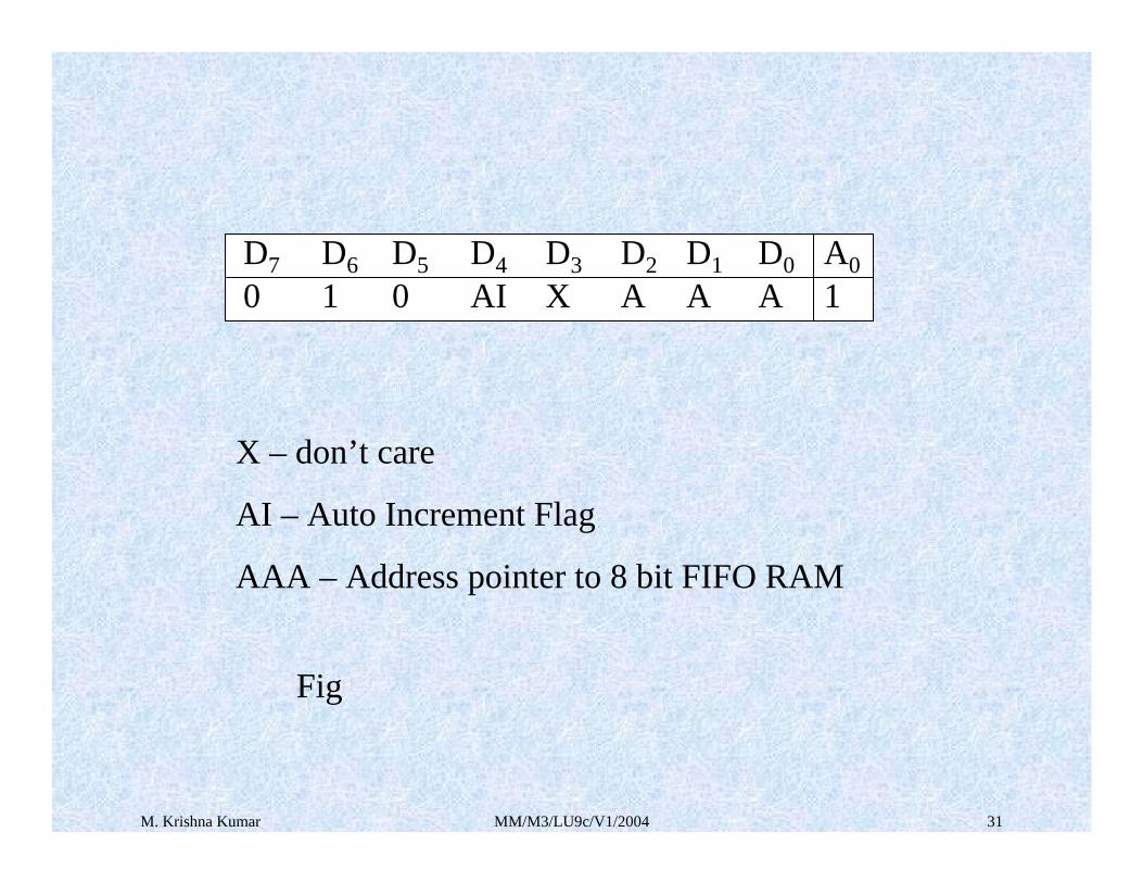
c) Read FIFO / Sensor RAM : The format of this command is given below.
• This word is written to set up 8279 for reading FIFO/ sensor RAM. In scanned keyboard mode, AI and AAA bits are of no use. The 8279 will automatically drive data bus for each subsequent read, in the same sequence, in which the data was entered.
• In sensor matrix mode, the bits AAA select one of the 8 rows of RAM. If AI flag is set, each successive read will be from the subsequent RAM location.
Command Words of 8279 (cont..)
M. Krishna Kumar MM/M3/LU9c/V1/2004 31
D7 D6 D5 D4 D3 D2 D1 A0D00 1 0 AI X A A 1A
X – don’t care
AI – Auto Increment Flag
AAA – Address pointer to 8 bit FIFO RAM
Fig
M. Krishna Kumar MM/M3/LU9c/V1/2004 32
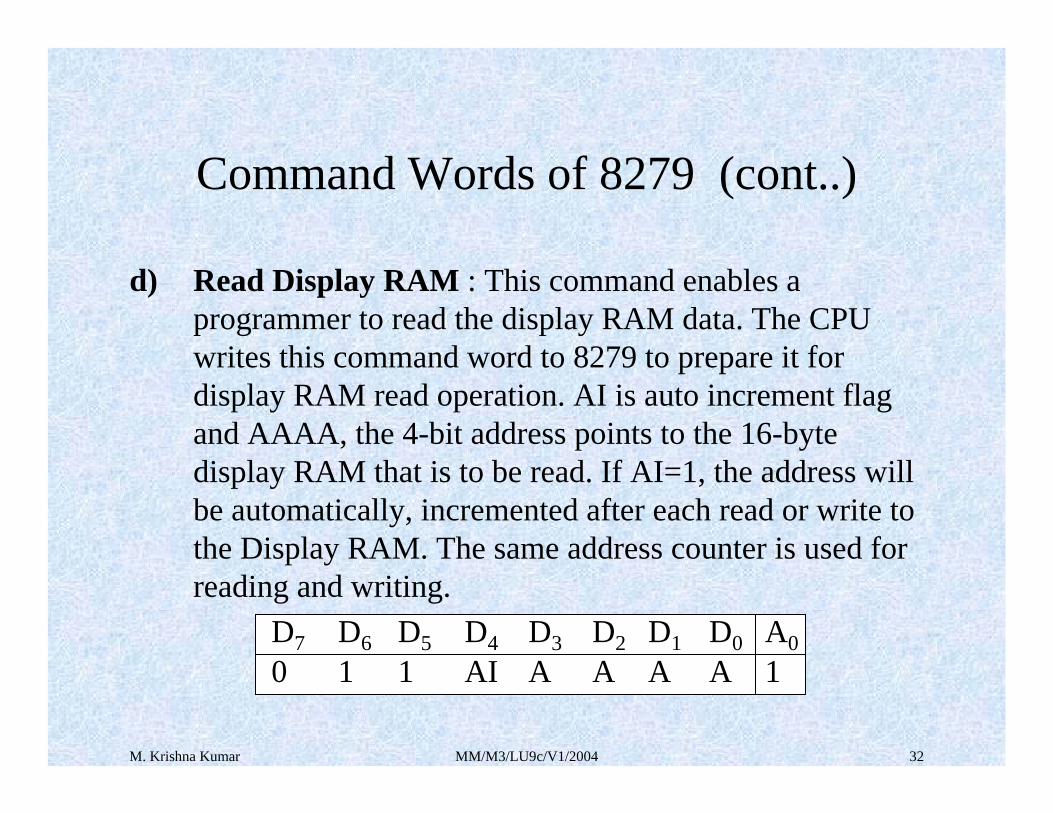
d) Read Display RAM : This command enables a programmer to read the display RAM data. The CPU writes this command word to 8279 to prepare it for display RAM read operation. AI is auto increment flag and AAAA, the 4-bit address points to the 16-byte display RAM that is to be read. If AI=1, the address will be automatically, incremented after each read or write to the Display RAM. The same address counter is used for reading and writing.
D7 D6 D5 D4 D3 D2 D1 A0D00 1 1 AI A A A 1A
Command Words of 8279 (cont..)

M. Krishna Kumar MM/M3/LU9c/V1/2004 33
e) Write Display RAM :
AI – Auto increment Flag.AAAA – 4 bit address for 16-bit display RAM to be written.
D7 D6 D5 D4 D3 D2 D1 A0D01 0 0 AI A A A 1A
Command Words of 8279 (cont..)

M. Krishna Kumar MM/M3/LU9c/V1/2004 34
f) Display Write Inhibit/Blanking : The IW ( inhibit write flag ) bits are used to mask the individual nibble as shown in the below command word. The output lines are divided into two nibbles ( OUTA0 – OUTA3 ) and ( OUTB0 – OUTB3 ), those can be masked by setting the corresponding IW bit to 1.
• Once a nibble is masked by setting the corresponding IW bit to 1, the entry to display RAM does not affect the nibble even though it may change the unmasked nibble. The blank display bit flags (BL) are used for blanking A and B nibbles.
Command Words of 8279 (cont..)
M. Krishna Kumar MM/M3/LU9c/V1/2004 35
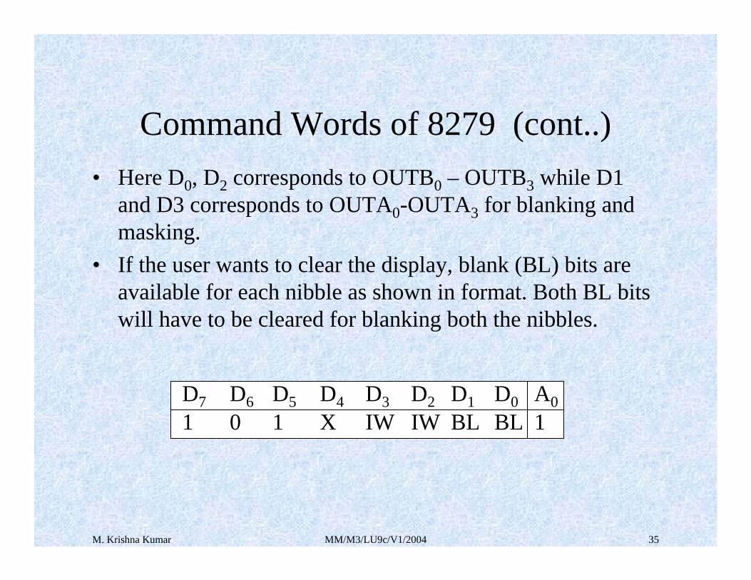
• Here D0, D2 corresponds to OUTB0 – OUTB3 while D1 and D3 corresponds to OUTA0-OUTA3 for blanking and masking.
• If the user wants to clear the display, blank (BL) bits are available for each nibble as shown in format. Both BL bits will have to be cleared for blanking both the nibbles.
D7 D6 D5 D4 D3 D2 D1 A0D01 0 1 X IW IW BL 1BL
Command Words of 8279 (cont..)

M. Krishna Kumar MM/M3/LU9c/V1/2004 36
g) Clear Display RAM : The CD2, CD1, CD0 is a selectable blanking code to clear all the rows of the display RAM as given below. The characters A and B represents the output nibbles.
• CD2 must be 1 for enabling the clear display command. If CD2 = 0, the clear display command is invoked by setting CA=1 and maintaining CD1, CD0 bits exactly same as above. If CF=1, FIFO status is cleared and IRQ line is pulled down.
• Also the sensor RAM pointer is set to row 0. if CA=1, this combines the effect of CD and CF bits. Here, CA represents Clear All and CF as Clear FIFO RAM.
Command Words of 8279 (cont..)

M. Krishna Kumar MM/M3/LU9c/V1/2004 37
D7 D6 D5 D4 D3 D2 D1 A0D01 1 0 CD2 CD1 CD0 CF 1CA
CD2 CD1 CD0
1 0 X
1 1 0
1 1 1
All zeros ( x don’t care ) AB=00
A3-A0 =2 (0010) and B3-B0=00 (0000)
All ones (AB =FF), i.e. clear RAM
Fig

M. Krishna Kumar MM/M3/LU9c/V1/2004 38
h) End Interrupt / Error mode Set : For the sensor matrix mode, this command lowers the IRQ line and enables further writing into the RAM. Otherwise, if a change in sensor value is detected, IRQ goes high that inhibits writing in the sensor RAM.
• For N-Key roll over mode, if the E bit is programmed to be ‘1’, the 8279 operates in special Error mode. Details of this mode are described in scanned keyboard special error mode. X- don’t care.
D7 D6 D5 D4 D3 D2 D1 A0D01 1 1 E X X X 1X
Command Words of 8279 (cont..)

M. Krishna Kumar MM/M3/LU9c/V1/2004 39
8
4
4
8086
8279
INTR
AD0-AD15A16-A19
RDWR
PCLK (from 8284)
Address decoder
8282 (3) Address latch
8259 Interrupt controller
A0L
A1L-A3L
A0L-A19L
INT2Shift
Control Key board matrix
8 columns8 rows
8
3-8 decoder
4-16 decoder
AddressDisplay character data
Blank display
BD
A0-3B0-3CLKA0
CSResetIOWIOR
INT
D0-7
RL0-7
S0-3
5VVDD
Vss 0VScan lines
Return lines
16
4
3
Data bus
Fig