700MHz, Crystal-to-3.3V Differential 8432I-51 LVPECL ...
22
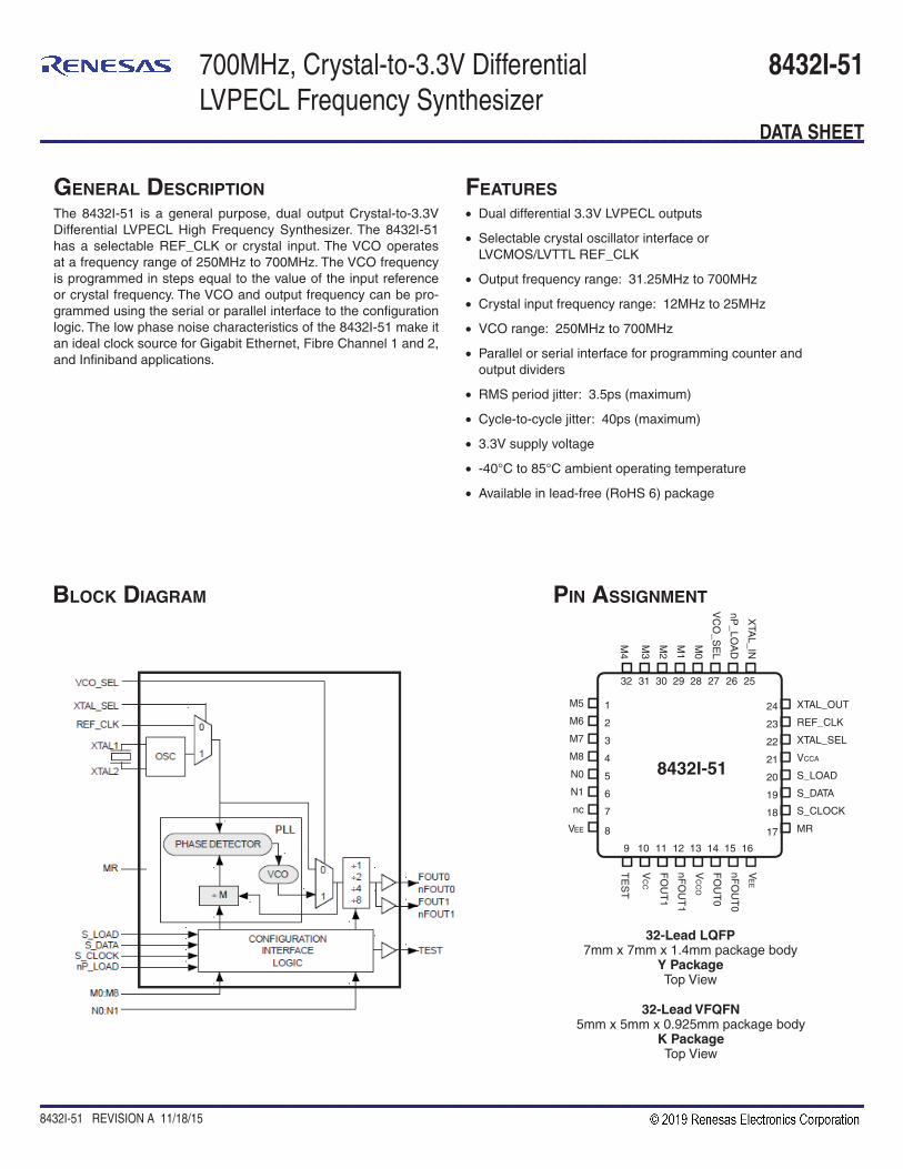
700MHz, Crystal-to-3.3V Differential LVPECL Frequency Synthesizer 8432I-51 DATA SHEET 8432I-51 REVISION A 11/18/15 1 ©2015 Integrated Device Technology, Inc. GENERAL DESCRIPTION The 8432I-51 is a general purpose, dual output Crystal-to-3.3V Differential LVPECL High Frequency Synthesizer. The 8432I-51 has a selectable REF_CLK or crystal input. The VCO operates at a frequency range of 250MHz to 700MHz. The VCO frequency is programmed in steps equal to the value of the input reference or crystal frequency. The VCO and output frequency can be pro- grammed using the serial or parallel interface to the configuration logic. The low phase noise characteristics of the 8432I-51 make it an ideal clock source for Gigabit Ethernet, Fibre Channel 1 and 2, and Infiniband applications. BLOCK DIAGRAM PIN ASSIGNMENT FEATURES • Dual differential 3.3V LVPECL outputs • Selectable crystal oscillator interface or LVCMOS/LVTTL REF_CLK • Output frequency range: 31.25MHz to 700MHz • Crystal input frequency range: 12MHz to 25MHz • VCO range: 250MHz to 700MHz • Parallel or serial interface for programming counter and output dividers • RMS period jitter: 3.5ps (maximum) • Cycle-to-cycle jitter: 40ps (maximum) • 3.3V supply voltage • -40°C to 85°C ambient operating temperature • Available in lead-free (RoHS 6) package 32 31 30 29 28 27 26 25 9 10 11 12 13 14 15 16 1 2 3 4 5 6 7 8 24 23 22 21 20 19 18 17 XTAL_OUT REF_CLK XTAL_SEL VCCA S_LOAD S_DATA S_CLOCK MR M5 M6 M7 M8 N0 N1 nc VEE VEE nFOUT0 FOUT0 VCCO nFOUT1 FOUT1 VCC TEST XTAL_IN nP_LOAD VCO_SEL M0 M1 M2 M3 M4 32-Lead LQFP 7mm x 7mm x 1.4mm package body Y Package Top View 8432I-51 32-Lead VFQFN 5mm x 5mm x 0.925mm package body K Package Top View
Transcript of 700MHz, Crystal-to-3.3V Differential 8432I-51 LVPECL ...
700MHz, Crystal-to-3.3V DifferentialLVPECL Frequency Synthesizer
8432I-51
DATA SHEET
8432I-51 REVISION A 11/18/15 1 ©2015 Integrated Device Technology, Inc.
GENERAL DESCRIPTIONThe 8432I-51 is a general purpose, dual output Crystal-to-3.3V Differential LVPECL High Frequency Synthesizer. The 8432I-51 has a selectable REF_CLK or crystal input. The VCO operates at a frequency range of 250MHz to 700MHz. The VCO frequency is programmed in steps equal to the value of the input reference or crystal frequency. The VCO and output frequency can be pro-grammed using the serial or parallel interface to the confi guration logic. The low phase noise characteristics of the 8432I-51 make it an ideal clock source for Gigabit Ethernet, Fibre Channel 1 and 2, and Infi niband applications.
BLOCK DIAGRAM PIN ASSIGNMENT
FEATURES• Dual differential 3.3V LVPECL outputs
• Selectable crystal oscillator interface orLVCMOS/LVTTL REF_CLK
• Output frequency range: 31.25MHz to 700MHz
• Crystal input frequency range: 12MHz to 25MHz
• VCO range: 250MHz to 700MHz
• Parallel or serial interface for programming counter andoutput dividers
• RMS period jitter: 3.5ps (maximum)
• Cycle-to-cycle jitter: 40ps (maximum)
• 3.3V supply voltage
• -40°C to 85°C ambient operating temperature
• Available in lead-free (RoHS 6) package
32 31 30 29 28 27 26 25
9 10 11 12 13 14 15 16
1
2
3
4
5
6
7
8
24
23
22
21
20
19
18
17
XTAL_OUT
REF_CLK
XTAL_SEL
VCCA
S_LOAD
S_DATA
S_CLOCK
MR
M5
M6
M7
M8
N0
N1
nc
VEE
VE
E
nFO
UT
0
FO
UT
0
VC
CO
nFO
UT
1
FO
UT
1
VC
C
TE
ST
XTA
L_IN
nP_LO
AD
VC
O_S
EL
M0
M1
M2
M3
M4
32-Lead LQFP7mm x 7mm x 1.4mm package body
Y PackageTop View
8432I-51
32-Lead VFQFN5mm x 5mm x 0.925mm package body
K PackageTop View
700MHZ, CYRSTAL-TO-3.3V DIFFERENTIALLVPECL FREQUENCY SYNTHESIZER
8432I-51 DATA SHEET
2 REVISION B 11/18/15
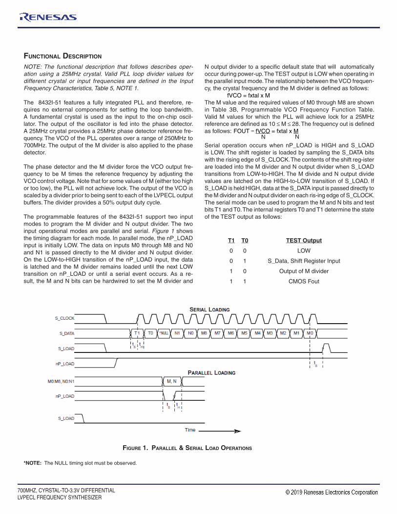
N output divider to a specifi c default state that will automatically occur during power-up. The TEST output is LOW when operating in the parallel input mode. The relationship between the VCO frequen-cy, the crystal frequency and the M divider is defi ned as follows:
The M value and the required values of M0 through M8 are shown in Table 3B, Programmable VCO Frequency Function Table. Valid M values for which the PLL will achieve lock for a 25MHz reference are defi ned as 10 ≤ M ≤ 28. The frequency out is defi ned as follows:
Serial operation occurs when nP_LOAD is HIGH and S_LOAD is LOW. The shift register is loaded by sampling the S_DATA bitswith the rising edge of S_CLOCK. The contents of the shift reg-ister are loaded into the M divider and N output divider when S_LOAD transitions from LOW-to-HIGH. The M divide and N output divide values are latched on the HIGH-to-LOW transition of S_LOAD. If S_LOAD is held HIGH, data at the S_DATA input is passed directly to the M divider and N output divider on each ris-ing edge of S_CLOCK. The serial mode can be used to program the M and N bits and test bits T1 and T0. The internal registers T0 and T1 determine the state of the TEST output as follows:
FUNCTIONAL DESCRIPTION
NOTE: The functional description that follows describes oper-ation using a 25MHz crystal. Valid PLL loop divider values for different crystal or input frequencies are defined in the Input Frequency Characteristics, Table 5, NOTE 1.
The 8432I-51 features a fully integrated PLL and therefore, re-quires no external components for setting the loop bandwidth. A fundamental crystal is used as the input to the on-chip oscil-lator. The output of the oscillator is fed into the phase detector.A 25MHz crystal provides a 25MHz phase detector reference fre-quency. The VCO of the PLL operates over a range of 250MHz to 700MHz. The output of the M divider is also applied to the phase detector.
The phase detector and the M divider force the VCO output fre-quency to be M times the reference frequency by adjusting theVCO control voltage. Note that for some values of M (either too high or too low), the PLL will not achieve lock. The output of the VCO is scaled by a divider prior to being sent to each of the LVPECL output buffers. The divider provides a 50% output duty cycle.
The programmable features of the 8432I-51 support two input modes to program the M divider and N output divider. The two input operational modes are parallel and serial. Figure 1 shows the timing diagram for each mode. In parallel mode, the nP_LOAD input is initially LOW. The data on inputs M0 through M8 and N0 and N1 is passed directly to the M divider and N output divider. On the LOW-to-HIGH transition of the nP_LOAD input, the data is latched and the M divider remains loaded until the next LOW transition on nP_LOAD or until a serial event occurs. As a re-sult, the M and N bits can be hardwired to set the M divider and
fVCO = fxtal x M
T1 T0 TEST Output
0 0 LOW
0 1 S_Data, Shift Register Input
1 0 Output of M divider
1 1 CMOS Fout
FIGURE 1. PARALLEL & SERIAL LOAD OPERATIONS
*NOTE: The NULL timing slot must be observed.
FOUT = fVCO = fxtal x MN N
REVISION B 11/18/15
8432I-51 DATA SHEET
3 700MHZ, CYRSTAL-TO-3.3V DIFFERENTIALLVPECL FREQUENCY SYNTHESIZER
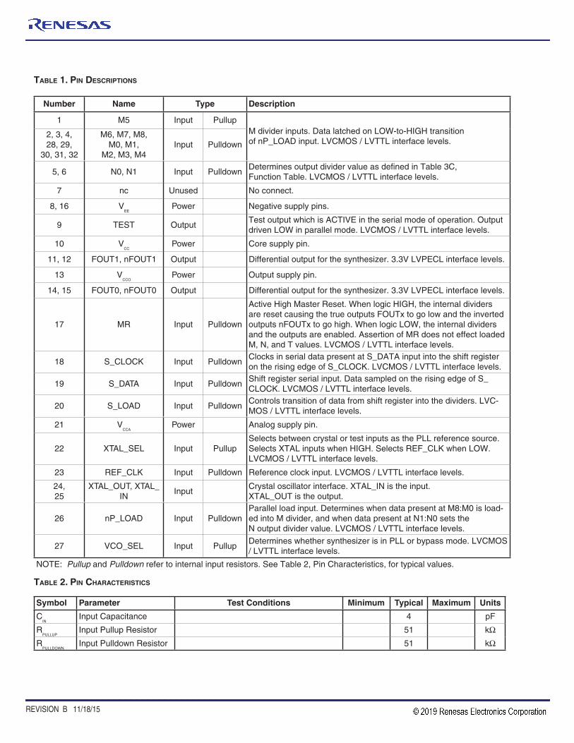
TABLE 1. PIN DESCRIPTIONS
Number Name Type Description
1 M5 Input PullupM divider inputs. Data latched on LOW-to-HIGH transitionof nP_LOAD input. LVCMOS / LVTTL interface levels.
2, 3, 4,28, 29,
30, 31, 32
M6, M7, M8,M0, M1,
M2, M3, M4Input Pulldown
5, 6 N0, N1 Input PulldownDetermines output divider value as defi ned in Table 3C,Function Table. LVCMOS / LVTTL interface levels.
7 nc Unused No connect.
8, 16 VEE
Power Negative supply pins.
9 TEST OutputTest output which is ACTIVE in the serial mode of operation. Output driven LOW in parallel mode. LVCMOS / LVTTL interface levels.
10 VCC
Power Core supply pin.
11, 12 FOUT1, nFOUT1 Output Differential output for the synthesizer. 3.3V LVPECL interface levels.
13 VCCO
Power Output supply pin.
14, 15 FOUT0, nFOUT0 Output Differential output for the synthesizer. 3.3V LVPECL interface levels.
17 MR Input Pulldown
Active High Master Reset. When logic HIGH, the internal dividers are reset causing the true outputs FOUTx to go low and the inverted outputs nFOUTx to go high. When logic LOW, the internal dividers and the outputs are enabled. Assertion of MR does not effect loaded M, N, and T values. LVCMOS / LVTTL interface levels.
18 S_CLOCK Input PulldownClocks in serial data present at S_DATA input into the shift register on the rising edge of S_CLOCK. LVCMOS / LVTTL interface levels.
19 S_DATA Input PulldownShift register serial input. Data sampled on the rising edge of S_CLOCK. LVCMOS / LVTTL interface levels.
20 S_LOAD Input PulldownControls transition of data from shift register into the dividers. LVC-MOS / LVTTL interface levels.
21 VCCA
Power Analog supply pin.
22 XTAL_SEL Input PullupSelects between crystal or test inputs as the PLL reference source. Selects XTAL inputs when HIGH. Selects REF_CLK when LOW.LVCMOS / LVTTL interface levels.
23 REF_CLK Input Pulldown Reference clock input. LVCMOS / LVTTL interface levels.
24,25
XTAL_OUT, XTAL_IN
InputCrystal oscillator interface. XTAL_IN is the input.XTAL_OUT is the output.
26 nP_LOAD Input PulldownParallel load input. Determines when data present at M8:M0 is load-ed into M divider, and when data present at N1:N0 sets theN output divider value. LVCMOS / LVTTL interface levels.
27 VCO_SEL Input PullupDetermines whether synthesizer is in PLL or bypass mode. LVCMOS / LVTTL interface levels.
NOTE: Pullup and Pulldown refer to internal input resistors. See Table 2, Pin Characteristics, for typical values.
TABLE 2. PIN CHARACTERISTICS
Symbol Parameter Test Conditions Minimum Typical Maximum Units
CIN
Input Capacitance 4 pF
RPULLUP
Input Pullup Resistor 51 kΩR
PULLDOWNInput Pulldown Resistor 51 kΩ
700MHZ, CYRSTAL-TO-3.3V DIFFERENTIALLVPECL FREQUENCY SYNTHESIZER
8432I-51 DATA SHEET
4 REVISION B 11/18/15
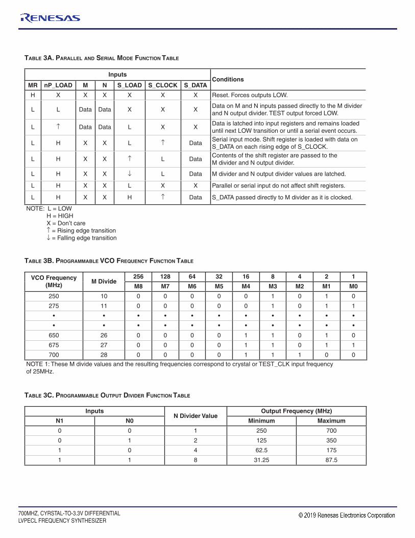
TABLE 3A. PARALLEL AND SERIAL MODE FUNCTION TABLE
InputsConditions
MR nP_LOAD M N S_LOAD S_CLOCK S_DATA
H X X X X X X Reset. Forces outputs LOW.
L L Data Data X X XData on M and N inputs passed directly to the M divider and N output divider. TEST output forced LOW.
L ↑ Data Data L X XData is latched into input registers and remains loaded until next LOW transition or until a serial event occurs.
L H X X L ↑ DataSerial input mode. Shift register is loaded with data on S_DATA on each rising edge of S_CLOCK.
L H X X ↑ L DataContents of the shift register are passed to theM divider and N output divider.
L H X X ↓ L Data M divider and N output divider values are latched.
L H X X L X X Parallel or serial input do not affect shift registers.
L H X X H ↑ Data S_DATA passed directly to M divider as it is clocked.
NOTE: L = LOW H = HIGH X = Don’t care ↑ = Rising edge transition ↓ = Falling edge transition
TABLE 3B. PROGRAMMABLE VCO FREQUENCY FUNCTION TABLE
TABLE 3C. PROGRAMMABLE OUTPUT DIVIDER FUNCTION TABLE
InputsN Divider Value
Output Frequency (MHz)
N1 N0 Minimum Maximum
0 0 1 250 700
0 1 2 125 350
1 0 4 62.5 175
1 1 8 31.25 87.5
VCO Frequency(MHz)
M Divide256 128 64 32 16 8 4 2 1
M8 M7 M6 M5 M4 M3 M2 M1 M0
250 10 0 0 0 0 0 1 0 1 0
275 11 0 0 0 0 0 1 0 1 1
• • • • • • • • • • •
• • • • • • • • • • •
650 26 0 0 0 0 1 1 0 1 0
675 27 0 0 0 0 1 1 0 1 1
700 28 0 0 0 0 1 1 1 0 0
NOTE 1: These M divide values and the resulting frequencies correspond to crystal or TEST_CLK input frequencyof 25MHz.
REVISION B 11/18/15
8432I-51 DATA SHEET
5 700MHZ, CYRSTAL-TO-3.3V DIFFERENTIALLVPECL FREQUENCY SYNTHESIZER
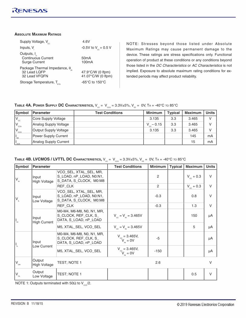
TABLE 4A. POWER SUPPLY DC CHARACTERISTICS, VCC
= VCCO
= 3.3V±5%, VEE
= 0V, TA = -40°C TO 85°C
TABLE 4B. LVCMOS / LVTTL DC CHARACTERISTICS, VCC
= VCCO
= 3.3V±5%, VEE
= 0V, TA = -40°C TO 85°C
Symbol Parameter Test Conditions Minimum Typical Maximum Units
VIH
InputHigh Voltage
VCO_SEL, XTAL_SEL, MR, S_LOAD, nP_LOAD, N0:N1, S_DATA, S_CLOCK, M0:M8
2 VCC
+ 0.3 V
REF_CLK 2 VCC
+ 0.3 V
VIL
InputLow Voltage
VCO_SEL, XTAL_SEL, MR, S_LOAD, nP_LOAD, N0:N1, S_DATA, S_CLOCK, M0:M8
-0.3 0.8 V
REF_CLK -0.3 1.3 V
IIH
InputHigh Current
M0-M4, M6-M8, N0, N1, MR, S_CLOCK, REF_CLK, S_DATA, S_LOAD, nP_LOAD
VCC
= VIN = 3.465V 150 µA
M5, XTAL_SEL, VCO_SEL VCC
= VIN = 3.465V 5 µA
IIL
InputLow Current
M0-M4, M6-M8, N0, N1, MR, S_CLOCK, REF_CLK, S_DATA, S_LOAD, nP_LOAD
VCC
= 3.465V,V
IN = 0V
-5 µA
M5, XTAL_SEL, VCO_SELV
CC = 3.465V,V
IN = 0V
-150 µA
VOH
OutputHigh Voltage
TEST; NOTE 1 2.6 V
VOL
OutputLow Voltage
TEST; NOTE 1 0.5 V
NOTE 1: Outputs terminated with 50Ω to VCCO
/2.
Symbol Parameter Test Conditions Minimum Typical Maximum Units
VCC
Core Supply Voltage 3.135 3.3 3.465 V
VCCA
Analog Supply Voltage VCC
– 0.15 3.3 3.465 V
VCCO
Output Supply Voltage 3.135 3.3 3.465 V
IEE
Power Supply Current 145 mA
ICCA
Analog Supply Current 15 mA
ABSOLUTE MAXIMUM RATINGS
Supply Voltage, VCC
4.6V
Inputs, VI -0.5V to V
CC + 0.5 V
Outputs, IO
Continuous Current 50mA Surge Current 100mA
Package Thermal Impedance, θJA
32 Lead LQFP 47.9°C/W (0 lfpm) 32 Lead VFQFN 41.07°C/W (0 lfpm)
Storage Temperature, TSTG
-65°C to 150°C
NOTE: Stresses beyond those l is ted under Absolute
Maximum Ratings may cause permanent damage to the
device. These ratings are stress specifi cations only. Functional
operation of product at these conditions or any conditions beyond
those listed in the DC Characteristics or AC Characteristics is not
implied. Exposure to absolute maximum rating conditions for ex-
tended periods may affect product reliability.
700MHZ, CYRSTAL-TO-3.3V DIFFERENTIALLVPECL FREQUENCY SYNTHESIZER
8432I-51 DATA SHEET
6 REVISION B 11/18/15
TABLE 4C. LVPECL DC CHARACTERISTICS, VCC
= VCCO
= 3.3V±5%, VEE
= 0V, TA = -40°C TO 85°C
Symbol Parameter Test Conditions Minimum Typical Maximum Units
VOH
Output High Voltage; NOTE 1 VCCO
- 1.4 VCCO
- 0.9 V
VOL
Output Low Voltage; NOTE 1 VCCO
- 2.0 VCCO
- 1.7 V
VSWING
Peak-to-Peak Output Voltage Swing 0.6 1.0 V
NOTE 1: Outputs terminated with 50 Ω to VCCO
- 2V. See “Parameter Measurement Information” section,fi gure “3.3V Output Load Test Circuit”.
TABLE 5. INPUT FREQUENCY CHARACTERISTICS, VCC
= VCCO
= 3.3V±5%, VEE
= 0V, TA = -40°C TO 85°C
Symbol Parameter Test Conditions Minimum Typical Maximum Units
fIN
Input Frequency
REF_CLK; NOTE 1 12 25 MHz
XTAL_IN, XTAL_OUT; NOTE 1
12 25 MHz
S_CLOCK 50 MHz
NOTE 1: For the input crystal and REF_CLK frequency range, the M value must be set for the VCO to operate within the 250MHz to 700MHz range. Using the minimum input frequency of 12MHz, valid values of M are 21 ≤ M ≤ 58. Using the maxi-mum frequency of 25MHz, valid values of M are 10 ≤ M ≤ 28.
TABLE 6. CRYSTAL CHARACTERISTICS
Symbol Parameter Test Conditions Minimum Typical Maximum Units
FOUT
Output Frequency 31.25 700 MHz
tjit(cc) Cycle-to-Cycle Jitter; NOTE 1, 3 fVCO > 350MHz 40 ps
tjit(per) Period Jitter, RMS; NOTE 1 3.5 ps
tsk(o) Output Skew; NOTE 2, 3 35 ps
tR / t
FOutput Rise/Fall Time 20% to 80% 200 700 ps
tS
Setup Time
M, N to nP_LOAD 5 ns
S_DATA to S_CLOCK 5 ns
S_CLOCK to S_LOAD 5 ns
tH
Hold Time
M, N to nP_LOAD 5 ns
S_DATA to S_CLOCK 5 ns
S_CLOCK to S_LOAD 5 ns
odc Output Duty Cycle N > 1 48 52 %
tPW
Output Pulse Width N = 1 tPERIOD
/2 - 150 tPERIOD
/2 + 150 ps
tLOCK
PLL Lock Time 1 ms
See Parameter Measurement Information section.NOTE 1: Jitter performance using XTAL inputs.NOTE 2: Defi ned as skew between outputs at the same supply voltage and with equal load conditions.Measured at the output differential cross points.NOTE 3: This parameter is defi ned in accordance with JEDEC Standard 65.
TABLE 7. AC CHARACTERISTICS, VCC
= VCCO
= 3.3V±5%, VEE
= 0V, TA = -40°C TO 85°C
Parameter Test Conditions Minimum Typical Maximum Units
Mode of Oscillation Fundamental
Frequency 12 25 MHz
Equivalent Series Resistance (ESR) 70 ΩShunt Capacitance 7 pF
Drive Level 1 mW
REVISION B 11/18/15
8432I-51 DATA SHEET
7 700MHZ, CYRSTAL-TO-3.3V DIFFERENTIALLVPECL FREQUENCY SYNTHESIZER
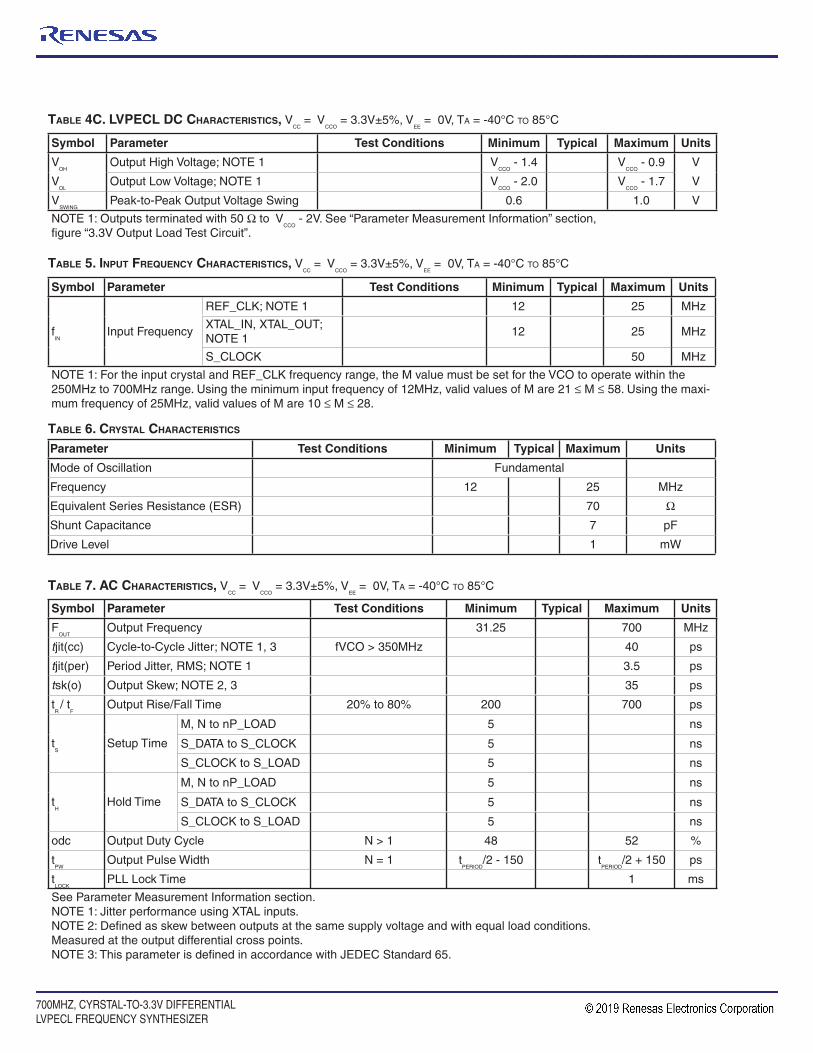
3.3V OUTPUT LOAD AC TEST CIRCUIT OUTPUT SKEW
CYCLE-TO-CYCLE JITTERPERIOD JITTER
OUTPUT DUTY CYCLE/PULSE WIDTH/PERIOD OUTPUT RISE/FALL TIME
PARAMETER MEASUREMENT INFORMATION
700MHZ, CYRSTAL-TO-3.3V DIFFERENTIALLVPECL FREQUENCY SYNTHESIZER
8432I-51 DATA SHEET
8 REVISION B 11/18/15
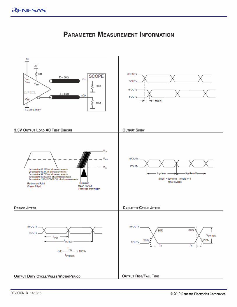
Table 8. Common SANs Application Frequencies
Table 9. Confi guration Details for SANs Applications
APPLICATION INFORMATION
As in any high speed analog circuitry, the power supply pins are vulnerable to random noise. To achieve optimum jitter perfor-mance, power supply isolation is required. The 8432I-51 provides separate power supplies to isolate any high switching noise from the outputs to the internal PLL. V
CC, V
CCA and V
CCO should be
individually connected to the power supply plane through vias, and 0.01µF bypass capacitors should be used for each pin.Figure 2 illustrates this for a generic V
CC pin and also shows that V
CCA
requires that an additional 10Ω resistor along with a 10µF bypass capacitor be connected to the V
CCA pin.
FIGURE 2. POWER SUPPLY FILTERING
Interconnect Technology Clock RateReference Frequency to SERDES
(MHz)Crystal Frequency
(MHz)
Gigabit Ethernet 1.25 GHz 125, 250, 156.25 25, 19.53125
Fibre ChannelFC1 1.0625 GHzFC2 2.1250 GHz
106.25, 53.125, 132.8125 16.6015625, 25
Infi niband 2.5 GHz 125, 250 25
POWER SUPPLY FILTERING TECHNIQUES
STORAGE AREA NETWORKS
A variety of technologies are used for interconnection of theelements within a SAN. The tables below lists the common
frequencies used as well as the settings for the 8432I-51 to generate the appropriate frequency.
Interconnect Technology
Crystal Frequency(MHz)
8432I-51Output Frequency
to SERDES(MHz)
8432I-51M & N Settings
M8 M7 M6 M5 M4 M3 M2 M1 M0 N1 N0
Gigabit Ethernet
25 125 0 0 0 0 1 0 1 0 0 1 0
25 250 0 0 0 0 1 0 1 0 0 0 1
25 156.25 0 0 0 0 1 1 0 0 1 1 0
19.53125 156.25 0 0 0 1 0 0 0 0 0 1 0
Fiber Channel 125 53.125 0 0 0 0 1 0 0 0 1 1 1
25 106.25 0 0 0 0 1 0 0 0 1 1 0
Fiber Channel 2 16.6015625 132.8125 0 0 0 1 0 0 0 0 0 1 0
Infi niband25 125 0 0 0 0 1 0 1 0 0 1 0
25 250 0 0 0 0 1 0 1 0 0 0 1
REVISION B 11/18/15
8432I-51 DATA SHEET
9 700MHZ, CYRSTAL-TO-3.3V DIFFERENTIALLVPECL FREQUENCY SYNTHESIZER
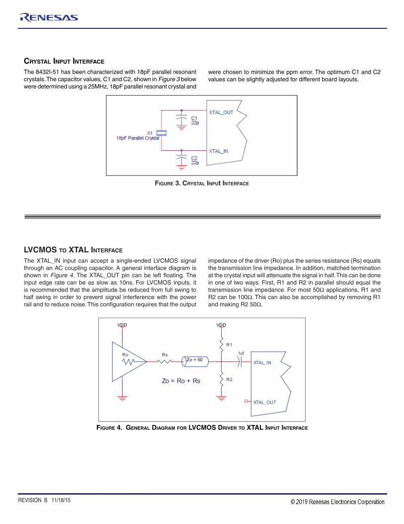
FIGURE 3. CRYSTAL INPUt INTERFACE
CRYSTAL INPUT INTERFACE
The 8432I-51 has been characterized with 18pF parallel resonant crystals. The capacitor values, C1 and C2, shown in Figure 3 below were determined using a 25MHz, 18pF parallel resonant crystal and
were chosen to minimize the ppm error. The optimum C1 and C2 values can be slightly adjusted for different board layouts.
LVCMOS TO XTAL INTERFACE
The XTAL_IN input can accept a single-ended LVCMOS signal through an AC coupling capacitor. A general interface diagram is shown in Figure 4. The XTAL_OUT pin can be left fl oating. The input edge rate can be as slow as 10ns. For LVCMOS inputs, it is recommended that the amplitude be reduced from full swing to half swing in order to prevent signal interference with the power rail and to reduce noise. This confi guration requires that the output
FIGURE 4. GENERAL DIAGRAM FOR LVCMOS DRIVER TO XTAL INPUT INTERFACE
impedance of the driver (Ro) plus the series resistance (Rs) equals the transmission line impedance. In addition, matched termination at the crystal input will attenuate the signal in half. This can be done in one of two ways. First, R1 and R2 in parallel should equal the transmission line impedance. For most 50Ω applications, R1 and R2 can be 100Ω. This can also be accomplished by removing R1 and making R2 50Ω.
R2
Zo = 50
VDD
Ro
Zo = Ro + Rs
R1
VDD
XTAL_IN
XTAL_OUT
.1ufRs
700MHZ, CYRSTAL-TO-3.3V DIFFERENTIALLVPECL FREQUENCY SYNTHESIZER
8432I-51 DATA SHEET
10 REVISION B 11/18/15
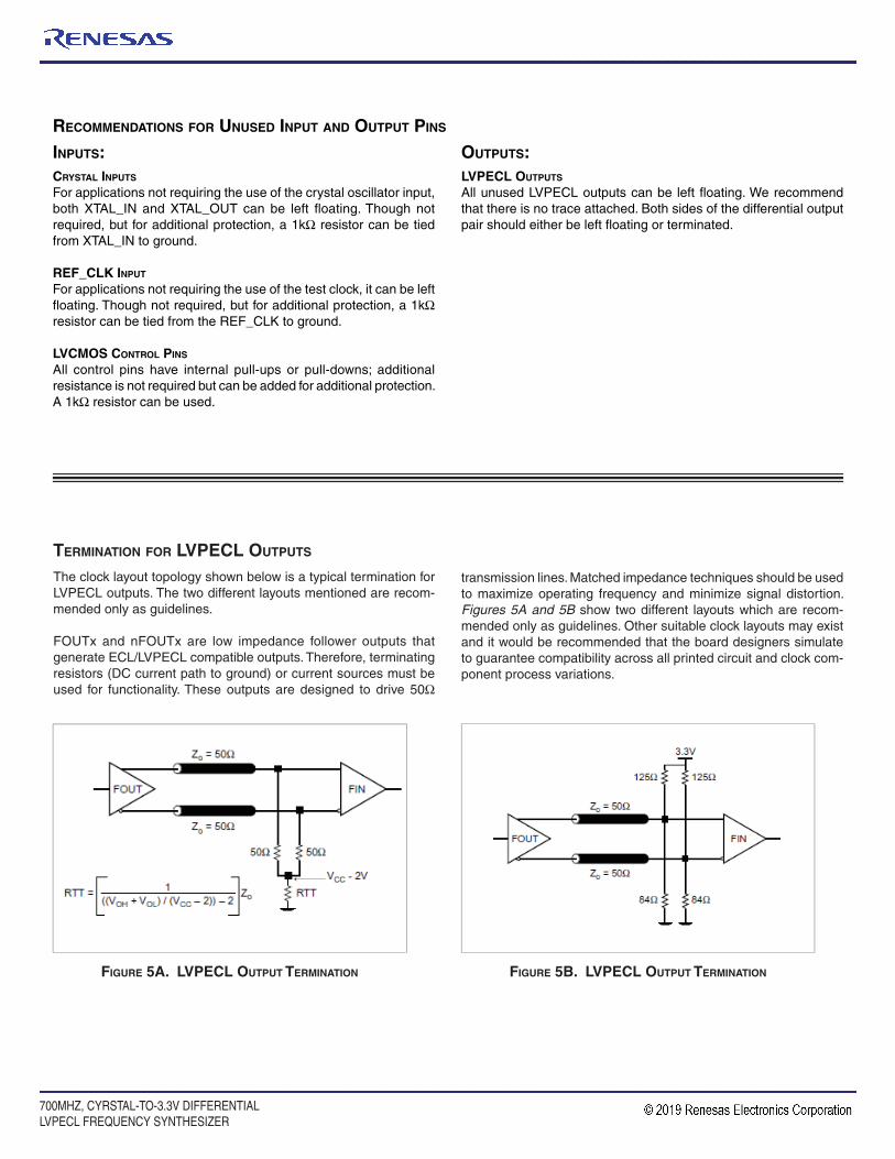
The clock layout topology shown below is a typical termination for LVPECL outputs. The two different layouts mentioned are recom-mended only as guidelines.
FOUTx and nFOUTx are low impedance follower outputs that generate ECL/LVPECL compatible outputs. Therefore, terminating resistors (DC current path to ground) or current sources must be used for functionality. These outputs are designed to drive 50Ω
FIGURE 5B. LVPECL OUTPUT TERMINATIONFIGURE 5A. LVPECL OUTPUT TERMINATION
transmission lines. Matched impedance techniques should be used to maximize operating frequency and minimize signal distortion. Figures 5A and 5B show two different layouts which are recom-mended only as guidelines. Other suitable clock layouts may exist and it would be recommended that the board designers simulate to guarantee compatibility across all printed circuit and clock com-ponent process variations.
TERMINATION FOR LVPECL OUTPUTS
INPUTS:CRYSTAL INPUTS For applications not requiring the use of the crystal oscillator input, both XTAL_IN and XTAL_OUT can be left fl oating. Though not required, but for additional protection, a 1kΩ resistor can be tied from XTAL_IN to ground.
REF_CLK INPUT
For applications not requiring the use of the test clock, it can be left fl oating. Though not required, but for additional protection, a 1kΩresistor can be tied from the REF_CLK to ground.
LVCMOS CONTROL PINS
All control pins have internal pull-ups or pull-downs; additional resistance is not required but can be added for additional protection. A 1kΩ resistor can be used.
RECOMMENDATIONS FOR UNUSED INPUT AND OUTPUT PINS
OUTPUTS:LVPECL OUTPUTS
All unused LVPECL outputs can be left fl oating. We recommend that there is no trace attached. Both sides of the differential output pair should either be left fl oating or terminated.
REVISION B 11/18/15
8432I-51 DATA SHEET
11 700MHZ, CYRSTAL-TO-3.3V DIFFERENTIALLVPECL FREQUENCY SYNTHESIZER
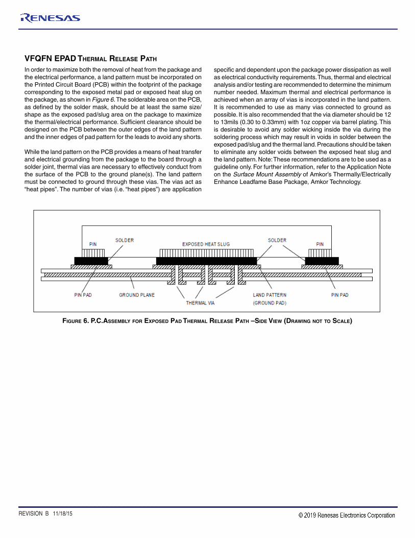
FIGURE 6. P.C.ASSEMBLY FOR EXPOSED PAD THERMAL RELEASE PATH –SIDE VIEW (DRAWING NOT TO SCALE)
VFQFN EPAD THERMAL RELEASE PATH
In order to maximize both the removal of heat from the package and the electrical performance, a land pattern must be incorporated on the Printed Circuit Board (PCB) within the footprint of the package corresponding to the exposed metal pad or exposed heat slug on the package, as shown in Figure 6. The solderable area on the PCB, as defi ned by the solder mask, should be at least the same size/shape as the exposed pad/slug area on the package to maximize the thermal/electrical performance. Suffi cient clearance should be designed on the PCB between the outer edges of the land pattern and the inner edges of pad pattern for the leads to avoid any shorts.
While the land pattern on the PCB provides a means of heat transfer and electrical grounding from the package to the board through a solder joint, thermal vias are necessary to effectively conduct from the surface of the PCB to the ground plane(s). The land pattern must be connected to ground through these vias. The vias act as “heat pipes”. The number of vias (i.e. “heat pipes”) are application
specifi c and dependent upon the package power dissipation as well as electrical conductivity requirements. Thus, thermal and electrical analysis and/or testing are recommended to determine the minimum number needed. Maximum thermal and electrical performance is achieved when an array of vias is incorporated in the land pattern. It is recommended to use as many vias connected to ground as possible. It is also recommended that the via diameter should be 12 to 13mils (0.30 to 0.33mm) with 1oz copper via barrel plating. This is desirable to avoid any solder wicking inside the via during the soldering process which may result in voids in solder between the exposed pad/slug and the thermal land. Precautions should be taken to eliminate any solder voids between the exposed heat slug and the land pattern. Note: These recommendations are to be used as a guideline only. For further information, refer to the Application Note on the Surface Mount Assembly of Amkor’s Thermally/Electrically Enhance Leadfame Base Package, Amkor Technology.
700MHZ, CYRSTAL-TO-3.3V DIFFERENTIALLVPECL FREQUENCY SYNTHESIZER
8432I-51 DATA SHEET
12 REVISION B 11/18/15
FIGURE 7A. SCHEMATIC OF RECOMMENDED LAYOUT
LAYOUT GUIDELINE
The schematic of the 8432I-51 layout example used in this layout guideline is shown in Figure 7A. The 8432I-51 recommended PCB board layout for this example is shown in Figure 7B. This layout example is used as a general guideline. The layout in the actual
system will depend on the selected component types, the density of the components, the density of the traces, and the stack up of the P.C. board.
S_DATA
FO
UT
N
VCCA
X1
R1125
U1
8432-51
12345678
9 10 11 12 13 14 15 16
1718192021222324
32 31 30 29 28 27 26 25
M5M6M7M8N0N1ncVEE
TE
ST
VC
CF
OU
T1
nFO
UT
1V
CC
OF
OU
T0
nFO
UT
0V
EE
MRS_CLOCK
S_DATAS_LOAD
VCCAnXTAL_SEL
REF_CLKX_OUT
M4
M3
M2
M1
M0
VC
O_S
EL
nP_L
OA
DX
_IN
C1610u
R3125
XTAL_SEL
R484
S_CLOCK
S_LOAD
FO
UT
C140.1u
VCC=3.3V
C150.1u
+
-
C11
0.01u
VCC
R284
VCC
REF_IN
VCC
TL1
Zo = 50 Ohm
C1
R710
TL2
Zo = 50 Ohm
C2
8432I-51
REVISION B 11/18/15
8432I-51 DATA SHEET
13 700MHZ, CYRSTAL-TO-3.3V DIFFERENTIALLVPECL FREQUENCY SYNTHESIZER
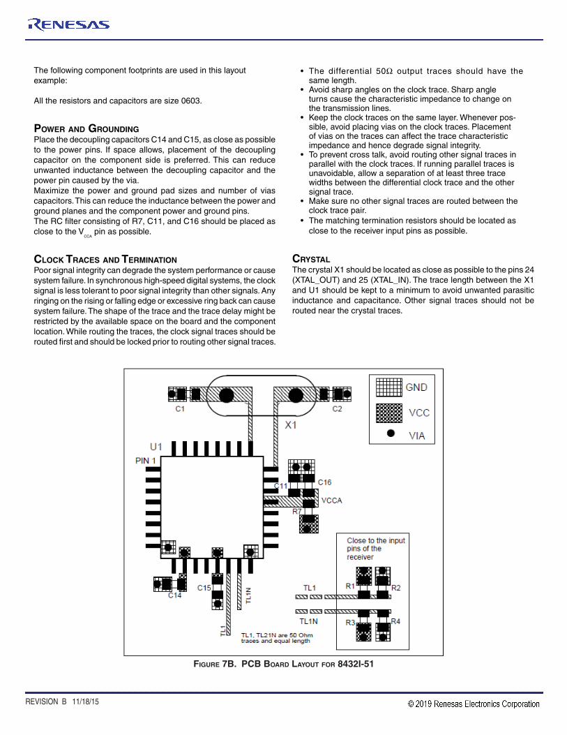
FIGURE 7B. PCB BOARD LAYOUT FOR 8432I-51
The following component footprints are used in this layoutexample:
All the resistors and capacitors are size 0603.
POWER AND GROUNDINGPlace the decoupling capacitors C14 and C15, as close as possible to the power pins. If space allows, placement of the decoupling capacitor on the component side is preferred. This can reduce unwanted inductance between the decoupling capacitor and the power pin caused by the via. Maximize the power and ground pad sizes and number of vias capacitors. This can reduce the inductance between the power and ground planes and the component power and ground pins.The RC fi lter consisting of R7, C11, and C16 should be placed as close to the V
CCA pin as possible.
CLOCK TRACES AND TERMINATIONPoor signal integrity can degrade the system performance or cause system failure. In synchronous high-speed digital systems, the clock signal is less tolerant to poor signal integrity than other signals. Any ringing on the rising or falling edge or excessive ring back can cause system failure. The shape of the trace and the trace delay might be restricted by the available space on the board and the component location. While routing the traces, the clock signal traces should be routed fi rst and should be locked prior to routing other signal traces.
• The differential 50Ω output traces should have the same length. • Avoid sharp angles on the clock trace. Sharp angle turns cause the characteristic impedance to change on the transmission lines. • Keep the clock traces on the same layer. Whenever pos- sible, avoid placing vias on the clock traces. Placement of vias on the traces can affect the trace characteristic impedance and hence degrade signal integrity. • To prevent cross talk, avoid routing other signal traces in parallel with the clock traces. If running parallel traces is unavoidable, allow a separation of at least three trace widths between the differential clock trace and the other signal trace. • Make sure no other signal traces are routed between the clock trace pair. • The matching termination resistors should be located as close to the receiver input pins as possible.
CRYSTALThe crystal X1 should be located as close as possible to the pins 24 (XTAL_OUT) and 25 (XTAL_IN). The trace length between the X1 and U1 should be kept to a minimum to avoid unwanted parasitic inductance and capacitance. Other signal traces should not be routed near the crystal traces.
700MHZ, CYRSTAL-TO-3.3V DIFFERENTIALLVPECL FREQUENCY SYNTHESIZER
8432I-51 DATA SHEET
14 REVISION B 11/18/15
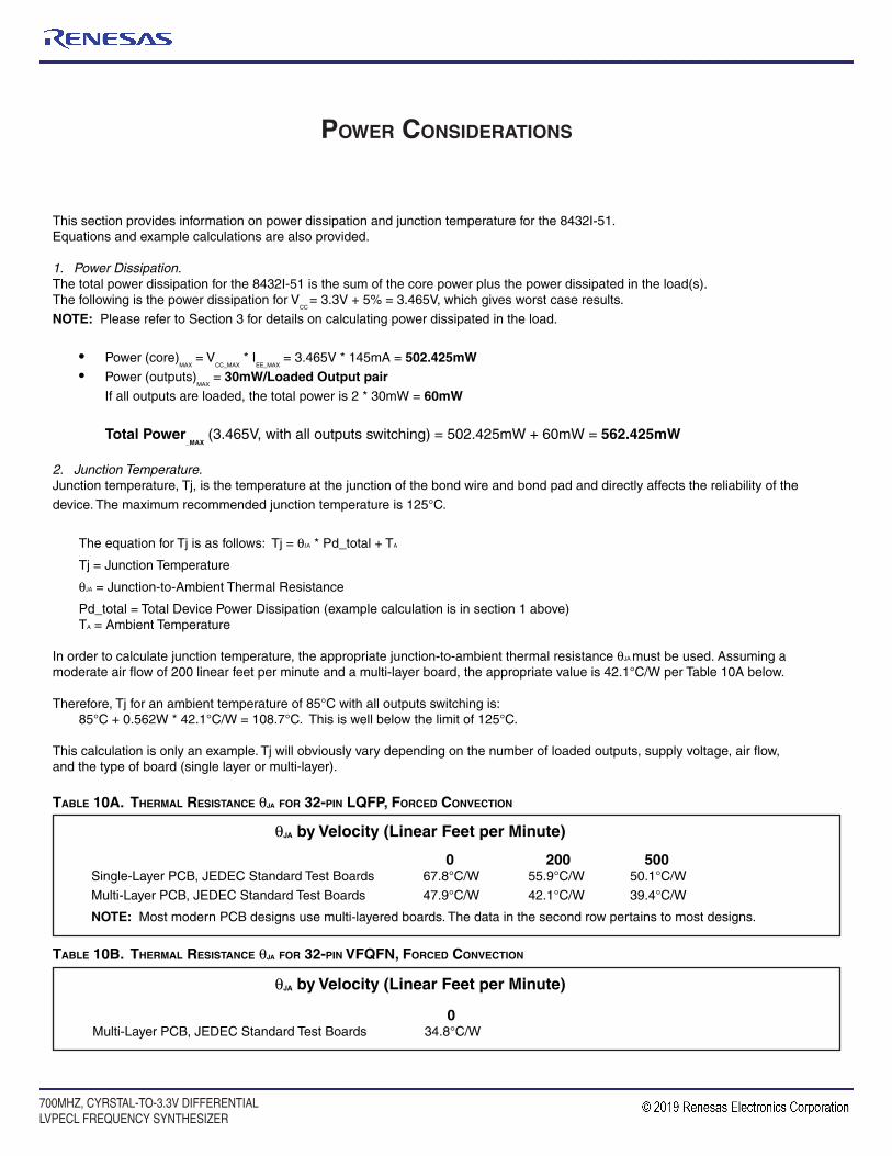
POWER CONSIDERATIONS
This section provides information on power dissipation and junction temperature for the 8432I-51. Equations and example calculations are also provided.
1. Power Dissipation. The total power dissipation for the 8432I-51 is the sum of the core power plus the power dissipated in the load(s). The following is the power dissipation for V
CC = 3.3V + 5% = 3.465V, which gives worst case results.
NOTE: Please refer to Section 3 for details on calculating power dissipated in the load.
• Power (core)MAX
= VCC_MAX
* IEE_MAX
= 3.465V * 145mA = 502.425mW• Power (outputs)
MAX = 30mW/Loaded Output pair
If all outputs are loaded, the total power is 2 * 30mW = 60mW
Total Power_MAX
(3.465V, with all outputs switching) = 502.425mW + 60mW = 562.425mW
2. Junction Temperature. Junction temperature, Tj, is the temperature at the junction of the bond wire and bond pad and directly affects the reliability of the
device. The maximum recommended junction temperature is 125°C.
The equation for Tj is as follows: Tj = θJA * Pd_total + TA
Tj = Junction Temperature
θJA = Junction-to-Ambient Thermal Resistance
Pd_total = Total Device Power Dissipation (example calculation is in section 1 above) TA = Ambient Temperature
In order to calculate junction temperature, the appropriate junction-to-ambient thermal resistance θJA must be used. Assuming a
moderate air fl ow of 200 linear feet per minute and a multi-layer board, the appropriate value is 42.1°C/W per Table 10A below.
Therefore, Tj for an ambient temperature of 85°C with all outputs switching is: 85°C + 0.562W * 42.1°C/W = 108.7°C. This is well below the limit of 125°C.
This calculation is only an example. Tj will obviously vary depending on the number of loaded outputs, supply voltage, air fl ow,and the type of board (single layer or multi-layer).
θJA by Velocity (Linear Feet per Minute)
0 200 500Single-Layer PCB, JEDEC Standard Test Boards 67.8°C/W 55.9°C/W 50.1°C/W
Multi-Layer PCB, JEDEC Standard Test Boards 47.9°C/W 42.1°C/W 39.4°C/W
NOTE: Most modern PCB designs use multi-layered boards. The data in the second row pertains to most designs.
TABLE 10A. THERMAL RESISTANCE θJA FOR 32-PIN LQFP, FORCED CONVECTION
θJA by Velocity (Linear Feet per Minute)
TABLE 10B. THERMAL RESISTANCE θJA FOR 32-PIN VFQFN, FORCED CONVECTION
0Multi-Layer PCB, JEDEC Standard Test Boards 34.8°C/W
REVISION B 11/18/15
8432I-51 DATA SHEET
15 700MHZ, CYRSTAL-TO-3.3V DIFFERENTIALLVPECL FREQUENCY SYNTHESIZER
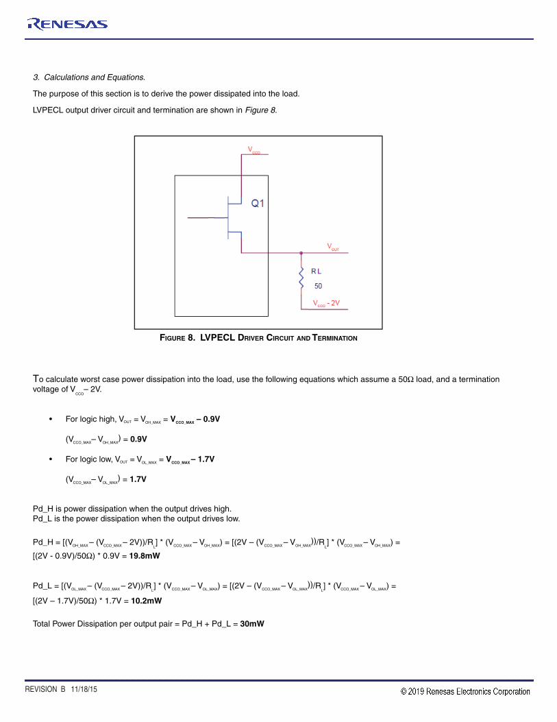
3. Calculations and Equations.
The purpose of this section is to derive the power dissipated into the load.
LVPECL output driver circuit and termination are shown in Figure 8.
To calculate worst case power dissipation into the load, use the following equations which assume a 50Ω load, and a terminationvoltage of V
CCO– 2V.
• For logic high, VOUT = VOH_MAX = VCCO_MAX – 0.9V
(VCCO_MAX– VOH_MAX) = 0.9V
• For logic low, VOUT = VOL_MAX = VCCO_MAX – 1.7V
(VCCO_MAX– VOL_MAX) = 1.7V
Pd_H is power dissipation when the output drives high.Pd_L is the power dissipation when the output drives low.
Pd_H = [(VOH_MAX – (VCCO_MAX
– 2V))/RL] * (VCCO_MAX
– VOH_MAX) = [(2V – (VCCO_MAX – VOH_MAX))/R
L] * (VCCO_MAX – VOH_MAX) =
[(2V - 0.9V)/50Ω) * 0.9V = 19.8mW
Pd_L = [(VOL_MAX – (VCCO_MAX – 2V))/R
L] * (VCCO_MAX – VOL_MAX) = [(2V – (VCCO_MAX – VOL_MAX
))/RL] * (VCCO_MAX – VOL_MAX) =
[(2V – 1.7V)/50Ω) * 1.7V = 10.2mW
Total Power Dissipation per output pair = Pd_H + Pd_L = 30mW
FIGURE 8. LVPECL DRIVER CIRCUIT AND TERMINATION
700MHZ, CYRSTAL-TO-3.3V DIFFERENTIALLVPECL FREQUENCY SYNTHESIZER
8432I-51 DATA SHEET
16 REVISION B 11/18/15
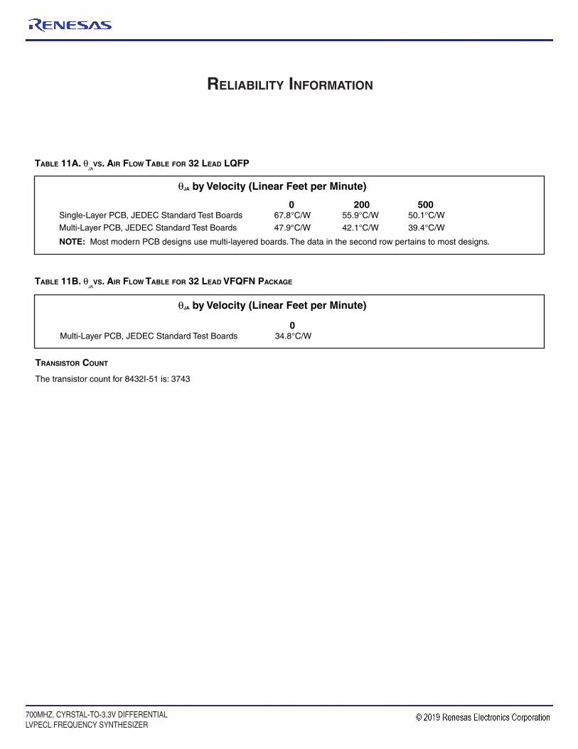
RELIABILITY INFORMATION
TRANSISTOR COUNT
The transistor count for 8432I-51 is: 3743
TABLE 11A. θJA
VS. AIR FLOW TABLE FOR 32 LEAD LQFP
TABLE 11B. θJA
VS. AIR FLOW TABLE FOR 32 LEAD VFQFN PACKAGE
θJA by Velocity (Linear Feet per Minute)
0 200 500Single-Layer PCB, JEDEC Standard Test Boards 67.8°C/W 55.9°C/W 50.1°C/W
Multi-Layer PCB, JEDEC Standard Test Boards 47.9°C/W 42.1°C/W 39.4°C/W
NOTE: Most modern PCB designs use multi-layered boards. The data in the second row pertains to most designs.
θJA by Velocity (Linear Feet per Minute)
0Multi-Layer PCB, JEDEC Standard Test Boards 34.8°C/W
REVISION B 11/18/15
8432I-51 DATA SHEET
17 700MHZ, CYRSTAL-TO-3.3V DIFFERENTIALLVPECL FREQUENCY SYNTHESIZER
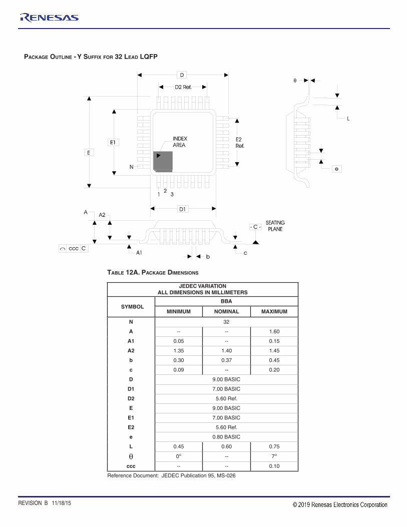
PACKAGE OUTLINE - Y SUFFIX FOR 32 LEAD LQFP
TABLE 12A. PACKAGE DIMENSIONS
Reference Document: JEDEC Publication 95, MS-026
JEDEC VARIATIONALL DIMENSIONS IN MILLIMETERS
SYMBOLBBA
MINIMUM NOMINAL MAXIMUM
N 32
A -- -- 1.60
A1 0.05 -- 0.15
A2 1.35 1.40 1.45
b 0.30 0.37 0.45
c 0.09 -- 0.20
D 9.00 BASIC
D1 7.00 BASIC
D2 5.60 Ref.
E 9.00 BASIC
E1 7.00 BASIC
E2 5.60 Ref.
e 0.80 BASIC
L 0.45 0.60 0.75
θ 0° -- 7°ccc -- -- 0.10
700MHZ, CYRSTAL-TO-3.3V DIFFERENTIALLVPECL FREQUENCY SYNTHESIZER
8432I-51 DATA SHEET
18 REVISION B 11/18/15
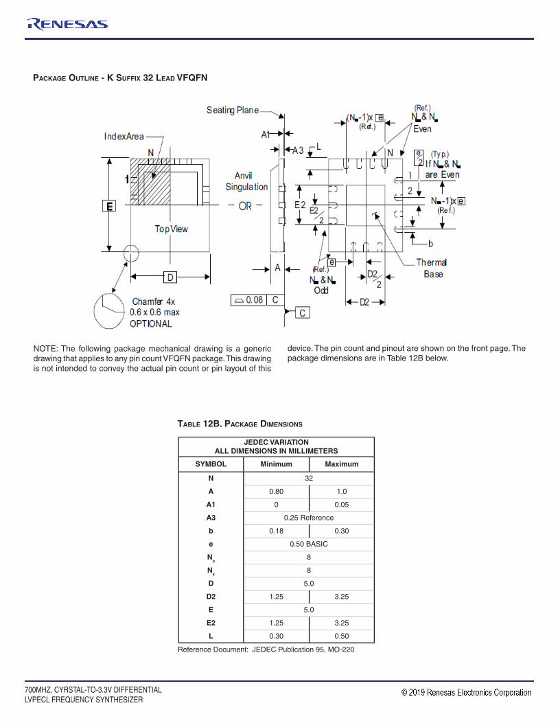
PACKAGE OUTLINE - K SUFFIX 32 LEAD VFQFN
TABLE 12B. PACKAGE DIMENSIONS
Reference Document: JEDEC Publication 95, MO-220
JEDEC VARIATIONALL DIMENSIONS IN MILLIMETERS
SYMBOL Minimum Maximum
N 32
A 0.80 1.0
A1 0 0.05
A3 0.25 Reference
b 0.18 0.30
e 0.50 BASIC
ND
8
NE
8
D 5.0
D2 1.25 3.25
E 5.0
E2 1.25 3.25
L 0.30 0.50
NOTE: The following package mechanical drawing is a generic drawing that applies to any pin count VFQFN package. This drawing is not intended to convey the actual pin count or pin layout of this
device. The pin count and pinout are shown on the front page. The package dimensions are in Table 12B below.
REVISION B 11/18/15
8432I-51 DATA SHEET
19 700MHZ, CYRSTAL-TO-3.3V DIFFERENTIALLVPECL FREQUENCY SYNTHESIZER
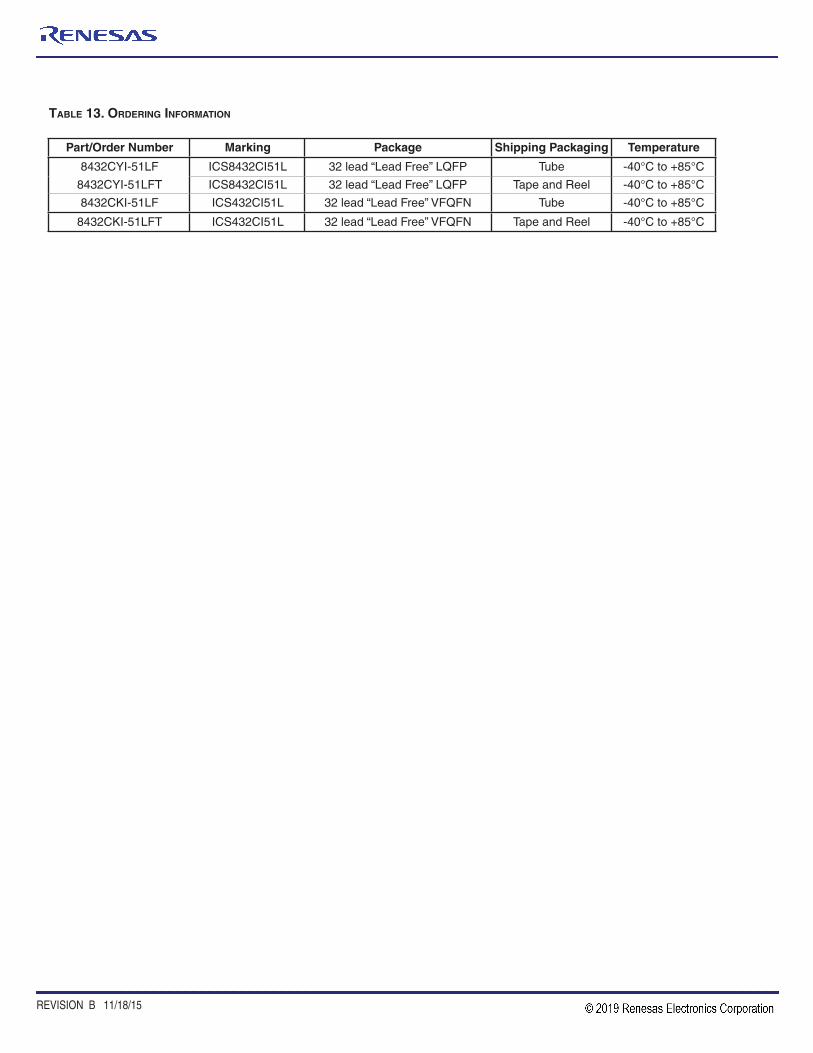
TABLE 13. ORDERING INFORMATION
Part/Order Number Marking Package Shipping Packaging Temperature
8432CYI-51LF ICS8432CI51L 32 lead “Lead Free” LQFP Tube -40°C to +85°C
8432CYI-51LFT ICS8432CI51L 32 lead “Lead Free” LQFP Tape and Reel -40°C to +85°C
8432CKI-51LF ICS432CI51L 32 lead “Lead Free” VFQFN Tube -40°C to +85°C
8432CKI-51LFT ICS432CI51L 32 lead “Lead Free” VFQFN Tape and Reel -40°C to +85°C
700MHZ, CYRSTAL-TO-3.3V DIFFERENTIALLVPECL FREQUENCY SYNTHESIZER
8432I-51 DATA SHEET
20 REVISION B 11/18/15
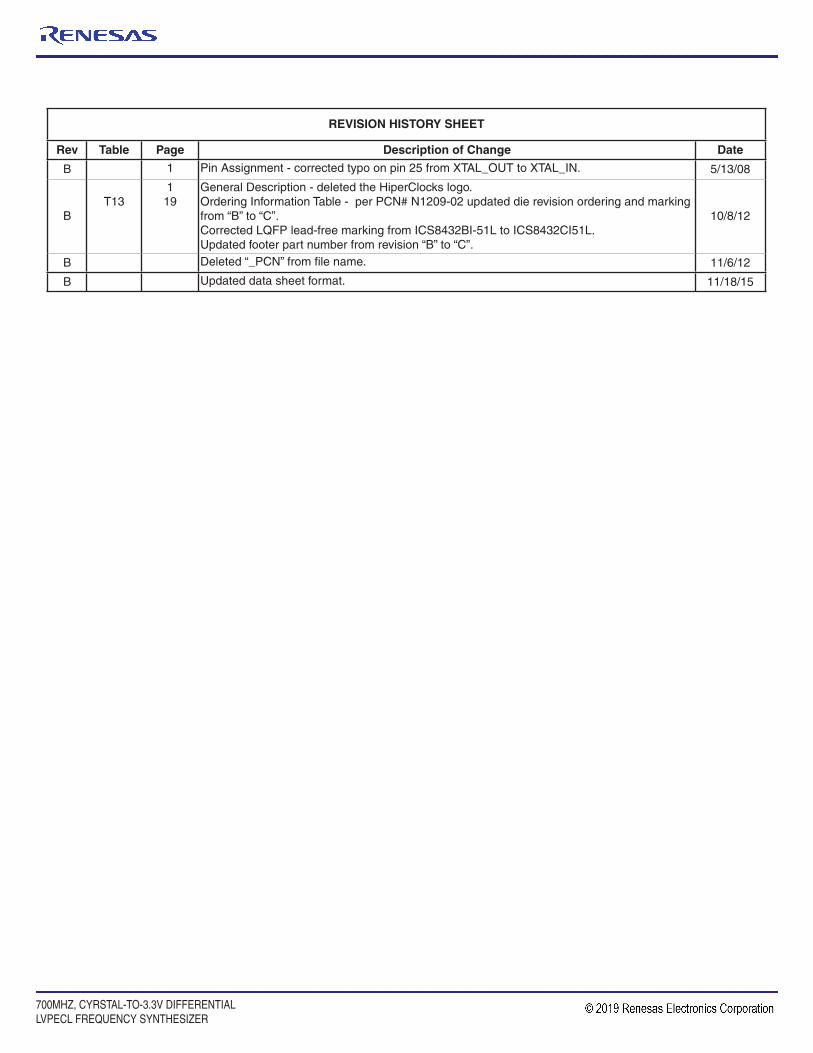
REVISION HISTORY SHEET
Rev Table Page Description of Change Date
B 1 Pin Assignment - corrected typo on pin 25 from XTAL_OUT to XTAL_IN. 5/13/08
BT13
119
General Description - deleted the HiperClocks logo.Ordering Information Table - per PCN# N1209-02 updated die revision ordering and marking from “B” to “C”.Corrected LQFP lead-free marking from ICS8432BI-51L to ICS8432CI51L.Updated footer part number from revision “B” to “C”.
10/8/12
B Deleted “_PCN” from fi le name. 11/6/12
B Updated data sheet format. 11/18/15

Corporate Headquarters6024 Silver Creek Valley Road San Jose, California 95138
Sales800-345-7015 or +408-284-8200Fax: 408-284-2775www.IDT.com
Technical Supportemail: [email protected]
DISCLAIMER Integrated Device Technology, Inc. (IDT) and its subsidiaries reserve the right to modify the products and/or specifi cations described herein at any time and at IDT’s sole discretion. All information in this document, including descriptions of product features and performance, is subject to change without notice. Performance specifi cations and the operating parameters of the described products are determined in the independent state and are not guaranteed to perform the same way when installed in customer products. The information contained herein is provided without representation or warranty of any kind, wheth-er express or implied, including, but not limited to, the suitability of IDT’s products for any particular purpose, an implied warranty of merchantability, or non-infringement of the intellectual property rights of others. This document is presented only as a guide and does not convey any license under intellectual property rights of IDT or any third parties.
IDT’s products are not intended for use in applications involving extreme environmental conditions or in life support systems or similar devices where the failure or malfunction of an IDT product can be reason-ably expected to signifi cantly affect the health or safety of users. Anyone using an IDT product in such a manner does so at their own risk, absent an express, written agreement by IDT.
Integrated Device Technology, IDT and the IDT logo are registered trademarks of IDT. Other trademarks and service marks used herein, including protected names, logos and designs, are the property of IDT or their respective third party owners.
Copyright 2015. All rights reserved.
Corporate HeadquartersTOYOSU FORESIA, 3-2-24 Toyosu,Koto-ku, Tokyo 135-0061, Japanwww.renesas.com
Contact InformationFor further information on a product, technology, the most up-to-date version of a document, or your nearest sales office, please visit:www.renesas.com/contact/
TrademarksRenesas and the Renesas logo are trademarks of Renesas Electronics Corporation. All trademarks and registered trademarks are the property of their respective owners.
IMPORTANT NOTICE AND DISCLAIMER
RENESAS ELECTRONICS CORPORATION AND ITS SUBSIDIARIES (“RENESAS”) PROVIDES TECHNICAL SPECIFICATIONS AND RELIABILITY DATA (INCLUDING DATASHEETS), DESIGN RESOURCES (INCLUDING REFERENCE DESIGNS), APPLICATION OR OTHER DESIGN ADVICE, WEB TOOLS, SAFETY INFORMATION, AND OTHER RESOURCES “AS IS” AND WITH ALL FAULTS, AND DISCLAIMS ALL WARRANTIES, EXPRESS OR IMPLIED, INCLUDING, WITHOUT LIMITATION, ANY IMPLIED WARRANTIES OF MERCHANTABILITY, FITNESS FOR A PARTICULAR PURPOSE, OR NON-INFRINGEMENT OF THIRD PARTY INTELLECTUAL PROPERTY RIGHTS.
These resources are intended for developers skilled in the art designing with Renesas products. You are solely responsible for (1) selecting the appropriate products for your application, (2) designing, validating, and testing your application, and (3) ensuring your application meets applicable standards, and any other safety, security, or other requirements. These resources are subject to change without notice. Renesas grants you permission to use these resources only for development of an application that uses Renesas products. Other reproduction or use of these resources is strictly prohibited. No license is granted to any other Renesas intellectual property or to any third party intellectual property. Renesas disclaims responsibility for, and you will fully indemnify Renesas and its representatives against, any claims, damages, costs, losses, or liabilities arising out of your use of these resources. Renesas' products are provided only subject to Renesas' Terms and Conditions of Sale or other applicable terms agreed to in writing. No use of any Renesas resources expands or otherwise alters any applicable warranties or warranty disclaimers for these products.
(Rev.1.0 Mar 2020)
© 2020 Renesas Electronics Corporation. All rights reserved.