Resistive Switching Behavior in Ferroelectric Heterostructures
description
Nanoscale heterojunctions
DOI: 10.1002/smll.200600727
The Synthesis and Fabrication of One-DimensionalNanoscale Heterojunctions&&All academic titles please&&Aneta J. Mieszawska, Romaneh Jalilian,Gamini U. Sumanasekera, and Francis P. Zamborini*
From the Contents
1. Introduction.................3
2. Vapor-Phase Methods. 5
3. Solution-Phase Methods..................................16
4. Template-DirectedSynthesis...................21
5. Other Methods...........28
6. Summary and FutureDirections..................30
Keywords:· heterojunctions· nanorods· nanostructures· nanowires· one-dimensional (1D)
2 www.small-journal.com � 2007 Wiley-VCH Verlag GmbH&Co. KGaA, Weinheim small 2007, 3, No.& , 2 – 36
�� These are not the final page numbers!
reviews F. P. Zamborini et al.
1 12 23 34 45 56 67 78 89 9
10 1011 1112 1213 1314 1415 1516 1617 1718 1819 1920 2021 2122 2223 2324 2425 2526 2627 2728 2829 2930 3031 3132 3233 3334 3435 3536 3637 3738 3839 3940 4041 4142 4243 4344 4445 4546 4647 4748 4849 4950 5051 5152 5253 5354 5455 5556 5657 5758 5859 59
There are a variety of methods for synthesizing or fabricating one-dimensional nanostructures containing heterojunctions between differentmaterials; such structures lead to unique properties and multifunctionalityuseful for a wide range of applications. Here we review recent developmentsin the synthesis and fabrication of such heterojunctions formed betweendifferent materials within the same 1D nanostructure or between different 1Dnanostructures comprised of different materials. Structures containing 1Dnanoscale heterojunctions exhibit interesting chemistry as well as size, shape,and material-dependent properties that are unique when compared to single-component materials. This leads to new or enhanced properties ormultifunctionality useful for a variety of applications in electronics,photonics, catalysis, and sensing, for example. This review separates themethods into vapor-phase synthesis, solution-phase synthesis, template-basedsynthesis, and other approaches, such as lithography, electrospinning, andassembly. These methods are used to form a variety of heterojunctions,including segmented, core/shell, branched, or crossed, from differentcombinations of semiconductor, metal, carbon, and polymeric materials.&&text changed somewhat or swapped for TOC and Abstract. OK?&&
1. Introduction
The synthesis of one-dimensional (1D) nanostruc-tures[1–13] has gained a tremendous amount of attention inrecent years due to their fascinating chemistry and size-,shape-, and material-dependent properties. Their interestingelectronic, optical, and magnetic properties, along withsmall size and chemical reactivity, have led to a wide rangeof applications in nanoelectronics, optoelectronics, plasmon-ics, medical diagnostics, catalysis, drug delivery, therapeutics,separations, and chemical sensing. There are many differentforms of 1D nanostructures, which are all characterized by ahigh aspect ratio (length-to-width). Nanorods (NRs) andnanowires (NWs) are the most common shape, differingonly by their aspect ratio (AR), which is commonly definedas <20 for NRs and �20 for NWs, respectively. Othercommon 1D shapes include tubes, ribbons, belts, whiskers,and needles. The physical properties greatly depend uponthe material, which can be metals, alloys, semiconductors,carbon, polymers, or molecular, but may also depend onshape, morphology, and structure (i.e., crystalline or amor-phous).
There have been two main types of studies on the prop-erties of 1D structures. The first includes those that measurethe collective properties of a solution or solid-state assemblyof numerous 1D structures. This requires the ability to syn-thesize large quantities of material with high uniformity andlow size dispersity in order to determine the structure andsize-dependent properties. For solid-state properties, it isalso necessary that the material be deposited as a film or as-sembled into an ordered array, and depending on the prop-erty, may also require control over alignment and orienta-tion of the assembly. One example of collective properties is
the optical spectrum of a solution of metallic 1D NRs orNWs of Ag and Au, which prominently display a transverseand AR-dependent longitudinal plasmon band.[14–16] Orient-ed, assembled arrays of Ag NWs and NRs display high sur-face-enhanced Raman scattering (SERS),[17–19] fluorescenceenhancement,[20] and plasmonic waveguiding properties,[21,22]
for example. Semiconductor NWs and carbon-nanotubearrays display properties useful for applications in nanoelec-tronics,[23] optoelectronics,[24] lasing,[25] sensing,[26, 27] and sepa-rations.[28]
The second type of study includes those that isolate andmeasure the properties of individual 1D nanostructures. Ex-cellent examples include electronic studies of individualcarbon nanotubes and Si NWs, which behave as field-effecttransistors[29–32] and electronic-based chemical or biologicalsensors.[33–35] There are also studies on the photoconductiveproperties of individual semiconductor NWs[36,37] and theeffect of molecular adsorption on the conductivity of indi-vidual metallic quantum wires.[38] These studies have had an
[*] &. a. t. p. J. Mieszawska, F. P. ZamboriniDepartment of Chemistry, University of LouisvilleLouisville, Kentucky 40292 (USA)Fax: (+1)502-852-8149E-mail: [email protected]
R. JalilianDepartment of Physics, University of LouisvilleLouisville, Kentucky 40292 (USA)
R. Jalilian, G. U. SumanasekeraDepartment of Electrical and Computer EngineeringUniversity of Louisville, Louisville, Kentucky 40292 (USA)
small 2007, 3, No.& , 2 – 36 � 2007 Wiley-VCH Verlag GmbH&Co. KGaA, Weinheim 3
These are not the final page numbers! ��
One-Dimensional Nanoscale Heterojunctions
1 12 23 34 45 56 67 78 89 9
10 1011 1112 1213 1314 1415 1516 1617 1718 1819 1920 2021 2122 2223 2324 2425 2526 2627 2728 2829 2930 3031 3132 3233 3334 3435 3536 3637 3738 3839 3940 4041 4142 4243 4344 4445 4546 4647 4748 4849 4950 5051 5152 5253 5354 5455 5556 5657 5758 5859 59
enormous impact on nanotechnology, demonstrating thegreat potential of these materials for a variety of applica-tions.
A natural progression from single-component materialshas been towards the synthesis and design of more complex,multicomponent 1D nanostructures. These multicomponentmaterials contain heterojunctions between various combina-tions of metals (M), semiconductors (SC), carbon (C), andpolymers (P) having a nanoscale 1D morphology. The for-mation of 1D heterojunctions has led to materials withunique properties and multiple functionalities not realizedin single-component structures that are useful for a widerange of applications. For example, the synthesis of p–njunctions formed from SC–SC 1D heterojunctions has re-sulted in current rectification[39] useful for logic gates, thefabrication of nanoscale photodetectors,[40] and functionallight-emitting diodes (LEDs).[41] M–SC–M heterojunctionNWs are photoconductive and M–M segmented 1D hetero-junctions have been used for biosensing,[42] gene delivery,[43]
separations,[44] and catalysis.[45] Other groups have synthe-sized segmented M–M 1D heterojunctions, where the differ-
ent segments possess different functions and properties,leading to the assembly of higher-order superstructures.[46,47]
Combining different materials into a 1D nanostructure ex-ploits the combined benefits of the 1D morphology with theunique function of the multicomponent heterojunction.
One of the most promising applications of 1D nano-structures in general, as shown in some of the examplesabove, has been in the area of electronics and photonics.Their small size potentially allows for higher-density elec-tronics, which could lead to smaller, more portable devicesor those with improved speed and performance. In additionto the size benefit, the small size of the structures oftenleads to vastly different properties compared to their bulkor 2D counterparts due to the higher surface-to-volumeratio of the material and quantum confinement effects.These properties are often tunable by the nanostructure sizeand offer more desirable properties for certain applications.Heterojunctions of 1D materials offer the same size andproperty benefit as single-component materials, but with theadded benefit of multifunctionality or new properties arisingfrom combining different materials, such as p–n junctions or
Aneta J. Mieszawska was born in Lublin,Poland. She obtained her MS degree in2002 in Environmental Protection fromthe Technical University of Lublin, study-ing “Effectiveness of Ozone on BTX-hy-drocarbon Oxidation”. She entered thegraduate program at the University ofLouisville (Louisville, KY) in the fall of2002, where she is currently pursuingher PhD in chemistry under the guidanceof Prof. F. P. Zamborini. Her research in-volves the synthesis, assembly, andalignment of gold nanorods and 1D
nanoscale heterojunctions (Au/GaAs, Au/ CNT and CNT/GaAs) direct-ly on surfaces and the study of their electronic and chemical-sensingproperties.
Editorial Advisory Board Member
Romaneh Jalilian received her BSc inphysics from Shahid Beheshti University(Tehran, Iran) in 2000 and MS in physicsat the University of Louisville (Louisville,KY) in 2004. The focus of her MS re-search was nanomaterials synthesis anddesign of vacuum systems for nanostruc-ture growth. She received the Manuel B.Schwartz Award for outstanding graduatestudent in May 2004. She is currently aPhD candidate in the Department ofElectrical Engineering at the University of
Louisville under the supervision of Prof. G. U. Sumanasekera. Thetopic of her dissertation is “Novel Properties of SemiconductingNanowires, Superlattices & Heterojunctions”. Her research interest isin the synthesis and characterization of semiconducting nanowiresand heterojunction nanostructures. She recently extended her skillson nanodevice fabrication for the electrical and optical characteriza-tion of nanostructures.
Gamini U. Sumanasekera received his BSfrom the University of Peradeniya (SriLanka) in 1980 and PhD from IndianaUniversity (Bloomington, IN) in 1995. Hethen worked as a research associate atPennsylvania State University (State Col-lege, PA) until he joined the faculty atthe University of Louisville (Louisville,KY) in 2002 as an Assistant Professor inthe Department of Physics. He also cur-rently serves as an associate facultymember in the Department of Electricaland Computer Engineering and as the
associate director for the Institute of Advanced Materials at the Uni-versity of Louisville. His research interests include the synthesis andcharacterization of nanostructres, including carbon nanotubes, inor-ganic nanowires, and 3D interconnected porous structures. He alsoconcentrates his research efforts on device fabrication, chemical sen-sors, thermoelectricity, and quantum transport.
Francis P. Zamborini received a BA inchemistry from Carthage College (Keno-sha, WI) in 1993 and a PhD in chemistryfrom Texas A&M University (College Sta-tion, TX) in 1998. Under the direction ofProf. R. M. Crooks, his doctoral researchfocused on the use of self-assembledmonolayers for corrosion passivationand nanolithography as studied by scan-ning probe microscopy, electrochemistry,and surface spectroscopy. He studiedunder Prof. R. W. Murray at the Universityof North Carolina (Chapel Hill, NC) as a
postdoctoral research associate from 1998–2001, focusing on as-sembly, electron transport, and chemical-sensing properties of goldnanoparticles. He joined the faculty at the University of Louisville in2001, where he is currently an Assistant Professor and member ofthe ElectroOptics Research Institute and Nanotechnology Center. Hisresearch interests are in the synthesis, assembly, and chemical-sens-ing properties of metal nanoparticles and 1D nanostructures.
4 www.small-journal.com � 2007 Wiley-VCH Verlag GmbH&Co. KGaA, Weinheim small 2007, 3, No.& , 2 – 36
�� These are not the final page numbers!
reviews F. P. Zamborini et al.
1 12 23 34 45 56 67 78 89 9
10 1011 1112 1213 1314 1415 1516 1617 1718 1819 1920 2021 2122 2223 2324 2425 2526 2627 2728 2829 2930 3031 3132 3233 3334 3435 3536 3637 3738 3839 3940 4041 4142 4243 4344 4445 4546 4647 4748 4849 4950 5051 5152 5253 5354 5455 5556 5657 5758 5859 59
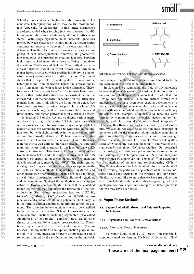
Schottky diodes. Another highly desirable property of 1Dnanoscale heterojunctions, which may be the most impor-tant (especially for electronics), is that lattice mismatchesare often avoided when forming junctions between two dif-ferent materials having substantially different lattice con-stants. With single-crystalline bulk materials, junctionsformed between materials with substantially different latticeconstants are subject to large misfit dislocations, which isdetrimental to the electronic performance of devices com-prised of such heterojunctions. Nanowire 1D geometries,however, offer the promise of creating junctions betweenhighly mismatched materials without suffering from thesedislocations. Matthews and Blakeslee[48] recently described acritical thickness model for misfit dislocations formed inplanar heterostructures, which predicts instability in a nano-wire heterojunction above a critical radius. The modelshows that it is possible to create perfect, dislocation-freeheterojunctions from nanowires below the critical radius,even from materials with a large lattice-mismatch. There-fore, one of the greatest benefits of nanowire heterojunc-tions is that misfit dislocations are nonexistent below thecritical radius of the nanowire (depending on the lattice mis-match). Importantly, this allows the formation of defect-freeheterojunctions from materials not possible in a larger 2Dgeometry, which may lead to novel properties, enhancedfunctionality, and higher performance of electronic devices.
In Sections 2–5 of this Review, we discuss various meth-ods for synthesizing or fabricating 1D heterojunctions. Vari-ous approaches used to synthesize single-component 1Dnanostructures are commonly used to synthesize 1D hetero-junctions, but with slight variations in the experimental pro-cedure. We broadly define a 1D heterojunction in thisreview as a 1D nanostructure comprised of more than onematerial with a well-defined interface between the differentmaterials, where both materials in the junction have a 1Danisotropic structure. This does not include junctions be-tween nanoparticles and 1D nanostructures, such as ZnSnanoparticles deposited on carbon nanotubes[49] or quantumdots deposited on semiconductor NWs.[50] The main synthet-ic categories fitting our definition include vapor-phase meth-ods, solution-phase methods, template-based synthesis, andother methods. Other methods include synthesis in super-critical fluids, lithography, assembly, solid–solid reactions,and electrospinning. Some of the methods involve a combi-nation of two or more methods. These will be classifiedunder the method that dominates the formation of the het-erojunction. The various approaches lead to: a) SC–SC,b) SC–M, c) M–M, d) C–C, e) C–M, and f) C–SC hetero-junctions, and junctions containing polymers. The C may bein the form of carbon nanotubes, amorphous carbon, or dia-mond. The different heterojunctions can also be classifiedby the nature of the junction. Scheme 1 shows some of themore common junctions, including segmented (also calledsuperlattices or end-to-end), core/shell (also called core/sheath or coaxial), 908 or angled cross sections (or T-junc-tions), hyperbranched, or other multibranched (“nano-brushes”) heterojunctions. The type of junction plays an im-portant role in the measured property or application and issometimes limited by the synthetic method or the material.
For example, template-based methods are limited to form-ing segmented or core/shell heterojunctions.
In Section 6 we summarize the field of 1D nanoscaleheterojunctions with general conclusions, limitations, futureoutlook, and challenges. It is important to note that thisReview does not include 1D heterojunctions formed withmolecules. There have been some exciting developments inthe growing field of molecular electronics and molecularwires with work published on 1D heterojunctions includingmolecules. For example, M–molecule–M junctions wereformed by combining electrochemical deposition, self-as-sembly, and electroless deposition in hard templates.[51]
However, this Review will not cover these types of exam-ples. We also do not cover all of the numerous examples ofpolymers and, for the most part, do not include examples ofjunctions defined by differences in structure or morphologywithin the same material. For example, Zhou et al. synthe-sized ZnO nanoplate–nanorod junctions[52] and Mather et al.synthesized crystalline Ge/nanocrystalline Ge core/shellstructures[53] that fit this description. We do cite some impor-tant examples of heterojunctions in CNTs and inorganicNWs formed by doping various segments[54–59] or assemblingcross junctions of metallic and semiconducting CNTs.[60]
This Review does not include detailed information about allof the exciting properties and applications of 1D heterojunc-tions because the focus is on the synthesis and fabrication.Finally, we would like to state that we have truly done ourbest to include all of the work in this fast-growing field andapologize for any important examples of heterojunctionsthat we may have overlooked.
2. Vapor-Phase Methods
2.1. Vapor–Liquid–Solid Growth and Catalyst-SupportedTechniques
2.1.1. Segmented and Branched Heterojunctions
2.1.1.1. Alternating Flow of Precursors
The vapor–liquid–solid (VLS) growth mechanism iscommonly used for forming 1D NWs of elemental, III–V,
Scheme 1. Different types of nanoscale 1D heterojunctions.
small 2007, 3, No.& , 2 – 36 � 2007 Wiley-VCH Verlag GmbH&Co. KGaA, Weinheim www.small-journal.com 5
These are not the final page numbers! ��
One-Dimensional Nanoscale Heterojunctions
1 12 23 34 45 56 67 78 89 9
10 1011 1112 1213 1314 1415 1516 1617 1718 1819 1920 2021 2122 2223 2324 2425 2526 2627 2728 2829 2930 3031 3132 3233 3334 3435 3536 3637 3738 3839 3940 4041 4142 4243 4344 4445 4546 4647 4748 4849 4950 5051 5152 5253 5354 5455 5556 5657 5758 5859 59
and II–VI semiconductors as well as metal oxides. There areseveral good reviews on the synthesis of 1D NWs by VLSand other vapor-phase growth mechanisms.[1,5, 6,9, 10] VLSgrowth can occur during different types of deposition meth-ods, including pulsed laser deposition (PLD), chemicalvapor deposition (CVD), metal–organic vapor-phase epitaxy(MOVPE), and chemical beam epitaxy (CBE), for example.For VLS growth to occur, the substrate must contain abound metal catalyst, which is typically a noble metal (i.e.,gold or silver) or other type of transition metal (i.e., nickelor iron). The growth process is held at elevated tempera-ture, usually 500–1200 8C, where the metal particle melts,forms a liquid-phase droplet, and alloys with reactantvapors. Reactant vapors concentrate preferentially on thecatalyst droplet and, with an increasing amount of reactantsin the system, the alloy becomes supersaturated, whichleads to nucleation and anisotropic crystallization of a NWthat retains the diameter of the catalyst/reactant droplet.For single-component NWs, this process occurs with justone type of precursor molecule or the appropriate combina-tion of precursors to form single-crystalline III–V or II–VIsemiconductors. To form segmented or core/shell 1D SC/SCheterojunction NWs, two (or more) different types of pre-cursors are introduced to the chamber in sequential fashionor all together at once as discussed in this Section and Sec-tion 2.1.1.2, respectively.
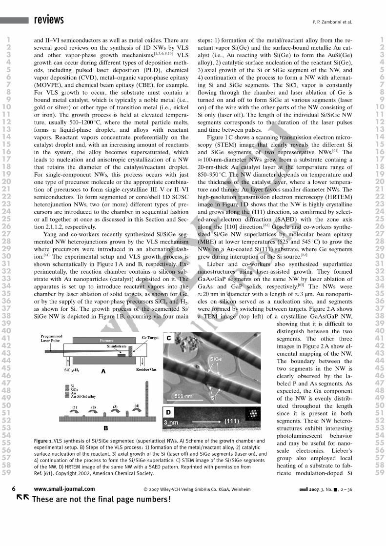
Yang and co-workers recently synthesized Si/SiGe seg-mented NW heterojunctions grown by the VLS mechanismwhere precursors were introduced in an alternating fash-ion.[61] The experimental setup and VLS growth process isshown schematically in Figure 1A and B, respectively. Ex-perimentally, the reaction chamber contains a silicon sub-strate with Au nanoparticles (catalyst) deposited on it. Theapparatus is set up to introduce reactant vapors into thechamber by laser ablation of solid targets, as shown for Ge,or by the supply of the vapor-phase precursors SiCl4 and H2,as shown for Si. The growth process of the segmented Si/SiGe NW is depicted in Figure 1B, occurring via four main
steps: 1) formation of the metal/reactant alloy from the re-actant vapor Si(Ge) and the surface-bound metallic Au cat-alyst (i.e., Au reacting with Si(Ge) to form the AuSi(Ge)alloy), 2) catalytic surface nucleation of the reactant Si(Ge),3) axial growth of the Si or SiGe segment of the NW, and4) continuation of the process to form a NW with alternat-ing Si and SiGe segments. The SiCl4 vapor is constantlyflowing through the chamber and laser ablation of Ge isturned on and off to form SiGe at various segments (laseron) of the wire with the other parts of the NW consisting ofSi only (laser off). The length of the individual Si/SiGe NWsegments corresponds to the duration of the laser pulsesand time between pulses.
Figure 1C shows a scanning transmission electron micro-scopy (STEM) image that clearly reveals the different Siand SiGe segments of two representative NWs.[61] The�100-nm-diameter NWs grew from a substrate containg a20-nm-thick Au catalyst layer at the temperature range of850–950 8C. The NW diameter depends on temperature andthe thickness of the catalyst layer, where a lower tempera-ture and thinner Au layer favors smaller diameter NWs. Thehigh-resolution transmission electron microscopy (HRTEM)image in Figure 1D shows that the NW is highly crystallineand grows along the (111) direction, as confirmed by select-ed-area electron diffraction (SAED) with the zone axisalong the [110] direction.[61] Gçsele and co-workers synthe-sized Si/Ge NW superlattices by molecular beam epitaxy(MBE) at lower temperatures (525 and 545 8C) to grow theNWs on a Au-coated SiACHTUNGTRENNUNG(111) substrate, where Ge segmentsgrew during interuption of the Si source.[62]
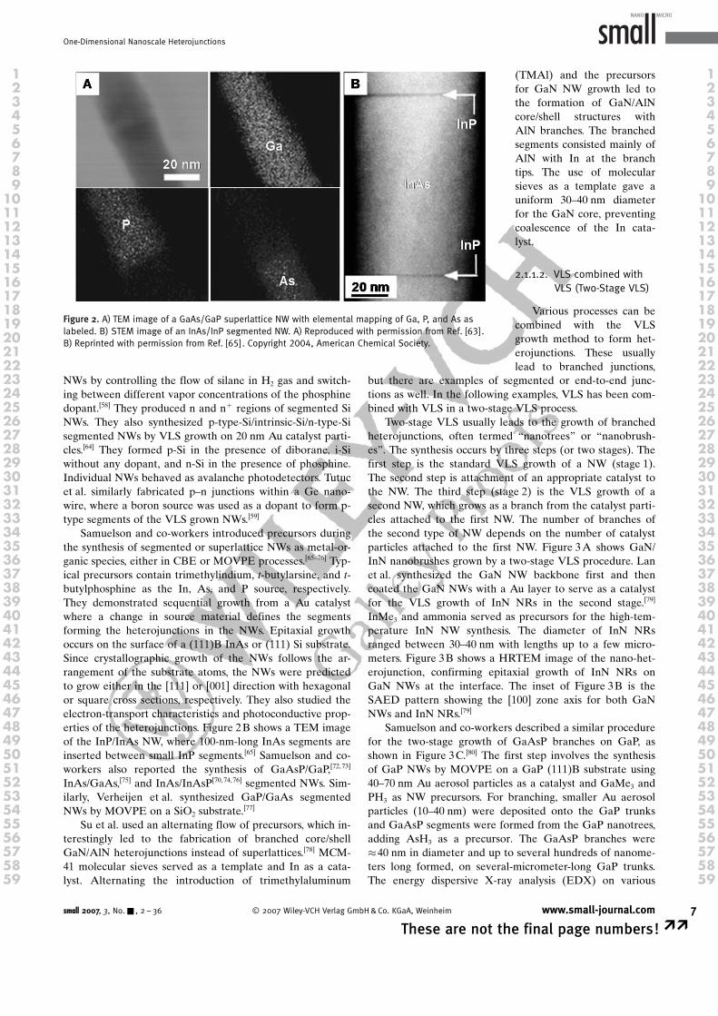
Lieber and co-workers also synthesized superlatticenanostructures using laser-assisted growth. They formedGaAs/GaP segments on the same NW by laser ablation ofGaAs and GaP solids, respectively.[63] The NWs were�20 nm in diameter with a length of �3 mm. Au nanoparti-cles on silicon served as a nucleation site, and segmentswere formed by switching between targets. Figure 2A showsa TEM image (top left) of a crystalline GaAs/GaP NW,
showing that it is difficult todistinguish between the twosegments. The other threeimages in Figure 2A show el-emental mapping of the NW.The boundary between thetwo segments in the NW isclearly observed by the la-beled P and As segments. Asexpected, the Ga componentof the NW is evenly distrib-uted throughout the lengthsince it is present in bothsegments. These NW hetero-structures exhibit interestingphotoluminescent behaviorand may be useful for nano-scale electronics. LieberGsgroup also employed localheating of a substrate to fab-ricate modulation-doped Si
Figure 1. VLS synthesis of Si/SiGe segmented (superlattice) NWs. A) Scheme of the growth chamber andexperimental setup. B) Steps of the VLS process: 1) formation of the metal/reactant alloy, 2) catalyticsurface nucleation of the reactant, 3) axial growth of the Si (laser off) and SiGe segments (laser on), and4) continuation of the process to form the Si/SiGe superlattice. C) STEM image of the Si/SiGe segmentsof the NW. D) HRTEM image of the same NW with a SAED pattern. Reprinted with permission fromRef. [61]. Copyright 2002, American Chemical Society.
6 www.small-journal.com � 2007 Wiley-VCH Verlag GmbH&Co. KGaA, Weinheim small 2007, 3, No.& , 2 – 36
�� These are not the final page numbers!
reviews F. P. Zamborini et al.
1 12 23 34 45 56 67 78 89 9
10 1011 1112 1213 1314 1415 1516 1617 1718 1819 1920 2021 2122 2223 2324 2425 2526 2627 2728 2829 2930 3031 3132 3233 3334 3435 3536 3637 3738 3839 3940 4041 4142 4243 4344 4445 4546 4647 4748 4849 4950 5051 5152 5253 5354 5455 5556 5657 5758 5859 59
NWs by controlling the flow of silane in H2 gas and switch-ing between different vapor concentrations of the phosphinedopant.[58] They produced n and n+ regions of segmented SiNWs. They also synthesized p-type-Si/intrinsic-Si/n-type-Sisegmented NWs by VLS growth on 20 nm Au catalyst parti-cles.[64] They formed p-Si in the presence of diborane, i-Siwithout any dopant, and n-Si in the presence of phosphine.Individual NWs behaved as avalanche photodetectors. Tutucet al. similarly fabricated p–n junctions within a Ge nano-wire, where a boron source was used as a dopant to form p-type segments of the VLS grown NWs.[59]
Samuelson and co-workers introduced precursors duringthe synthesis of segmented or superlattice NWs as metal-or-ganic species, either in CBE or MOVPE processes.[65–76] Typ-ical precursors contain trimethylindium, t-butylarsine, and t-butylphosphine as the In, As, and P source, respectively.They demonstrated sequential growth from a Au catalystwhere a change in source material defines the segmentsforming the heterojunctions in the NWs. Epitaxial growthoccurs on the surface of a (111)B InAs or (111) Si substrate.Since crystallographic growth of the NWs follows the ar-rangement of the substrate atoms, the NWs were predictedto grow either in the [111] or [001] direction with hexagonalor square cross sections, respectively. They also studied theelectron-transport characteristics and photoconductive prop-erties of the heterojunctions. Figure 2B shows a TEM imageof the InP/InAs NW, where 100-nm-long InAs segments areinserted between small InP segments.[65] Samuelson and co-workers also reported the synthesis of GaAsP/GaP,[72,73]
InAs/GaAs,[75] and InAs/InAsP[70,74,76] segmented NWs. Sim-ilarly, Verheijen et al. synthesized GaP/GaAs segmentedNWs by MOVPE on a SiO2 substrate.
[77]
Su et al. used an alternating flow of precursors, which in-terestingly led to the fabrication of branched core/shellGaN/AlN heterojunctions instead of superlattices.[78] MCM-41 molecular sieves served as a template and In as a cata-lyst. Alternating the introduction of trimethylaluminum
(TMAl) and the precursorsfor GaN NW growth led tothe formation of GaN/AlNcore/shell structures withAlN branches. The branchedsegments consisted mainly ofAlN with In at the branchtips. The use of molecularsieves as a template gave auniform 30–40 nm diameterfor the GaN core, preventingcoalescence of the In cata-lyst.
2.1.1.2. VLS combined withVLS (Two-Stage VLS)
Various processes can becombined with the VLSgrowth method to form het-erojunctions. These usuallylead to branched junctions,
but there are examples of segmented or end-to-end junc-tions as well. In the following examples, VLS has been com-bined with VLS in a two-stage VLS process.
Two-stage VLS usually leads to the growth of branchedheterojunctions, often termed “nanotrees” or “nanobrush-es”. The synthesis occurs by three steps (or two stages). Thefirst step is the standard VLS growth of a NW (stage 1).The second step is attachment of an appropriate catalyst tothe NW. The third step (stage 2) is the VLS growth of asecond NW, which grows as a branch from the catalyst parti-cles attached to the first NW. The number of branches ofthe second type of NW depends on the number of catalystparticles attached to the first NW. Figure 3A shows GaN/InN nanobrushes grown by a two-stage VLS procedure. Lanet al. synthesized the GaN NW backbone first and thencoated the GaN NWs with a Au layer to serve as a catalystfor the VLS growth of InN NRs in the second stage.[79]
InMe3 and ammonia served as precursors for the high-tem-perature InN NW synthesis. The diameter of InN NRsranged between 30–40 nm with lengths up to a few micro-meters. Figure 3B shows a HRTEM image of the nano-het-erojunction, confirming epitaxial growth of InN NRs onGaN NWs at the interface. The inset of Figure 3B is theSAED pattern showing the [100] zone axis for both GaNNWs and InN NRs.[79]
Samuelson and co-workers described a similar procedurefor the two-stage growth of GaAsP branches on GaP, asshown in Figure 3C.[80] The first step involves the synthesisof GaP NWs by MOVPE on a GaP (111)B substrate using40–70 nm Au aerosol particles as a catalyst and GaMe3 andPH3 as NW precursors. For branching, smaller Au aerosolparticles (10–40 nm) were deposited onto the GaP trunksand GaAsP segments were formed from the GaP nanotrees,adding AsH3 as a precursor. The GaAsP branches were�40 nm in diameter and up to several hundreds of nanome-ters long formed, on several-micrometer-long GaP trunks.The energy dispersive X-ray analysis (EDX) on various
Figure 2. A) TEM image of a GaAs/GaP superlattice NW with elemental mapping of Ga, P, and As aslabeled. B) STEM image of an InAs/InP segmented NW. A) Reproduced with permission from Ref. [63].B) Reprinted with permission from Ref. [65]. Copyright 2004, American Chemical Society.
small 2007, 3, No.& , 2 – 36 � 2007 Wiley-VCH Verlag GmbH&Co. KGaA, Weinheim www.small-journal.com 7
These are not the final page numbers! ��
One-Dimensional Nanoscale Heterojunctions
1 12 23 34 45 56 67 78 89 9
10 1011 1112 1213 1314 1415 1516 1617 1718 1819 1920 2021 2122 2223 2324 2425 2526 2627 2728 2829 2930 3031 3132 3233 3334 3435 3536 3637 3738 3839 3940 4041 4142 4243 4344 4445 4546 4647 4748 4849 4950 5051 5152 5253 5354 5455 5556 5657 5758 5859 59

parts of the “nanotrees” shows that the As component ispresent only in the branches grown during the second stage.This method produces heterojunctions with high controlover the density of branches either by controlling theamount of catalyst particles deposited on the first NW orthe number of branching levels. This group also grew InPbranches on GaP trunks.&&reference [80] as well?&&
Bae et al. synthesized various branched heterojunctionsof ZnO NRs on different materials.[81] They used thermalCVD to grow ZnO NRs onto presynthesized CNTs, GaN,GaP, SiC, and core/shell SiC/C 1D nanostructures grownalso by CVD on a solid substrate with appropriate catalysts.ZnO NRs grew by the VLS mechanism from powder mix-tures containing Zn with Ga or In serving as the catalyst.The substrate containing the presynthesized 1D nanostruc-tures was placed into the same boat with Zn and Ga or Inprecursors and growth of ZnO NRs occurred at 500 8C.They also introduced oxygen for ZnO formation. Figure 3Dshows branched heterojunctions of ZnO NRs grown onCNTs.[81] The CNT backbone is completely coated with theZnO NRs and difficult to observe in the image. The diame-ter of the ZnO NRs was 80 nm and the length 300 nm.
2.1.1.3. VLS combined with Other Methods
The VLS method has also been combined with carbon-nanotube synthesis, chemical assembly, and thermal meth-ods to form interesting heterojunctions. Carbon nanotubes(CNTs) are promising 1D materials for future applicationsin nanoelectronics and other nanoscale devices as they canbe metallic or semiconducting, depending on their chirality,
and they are mechanicallyvery strong. For these rea-sons, carbon has been com-monly incorporated into 1Dheterojunctions as shown inthe example for ZnO/CNTheterojunctions above. Simi-larily, in the following exam-ples, the attachment of cata-lyst particles to presynthe-sized CNTs and subsequentgrowth of NWs on the cata-lyst by the VLS mechanismleads to the formation ofCNT/SC heterojunctions. Forexample, Lieber and co-workers mounted MWCNTssynthesized by arc-dischargeat the end of a Pt–Ir scan-ning tunneling microscopy(STM) tip, and formed a het-erojunction with a Si NW, asshown in Figure 4A.[82] TheFESEM image shows theSTM tip on the left sidecoated with multiple CNTs.Au electrochemically depos-ited onto the end of the ex-
tended nanotube served as a catalyst for the VLS growth ofthe Si NW. The inset in Figure 4A is a TEM image of thejunction formed, confirming that the Si NW originates fromthe CNT. Lazareck et al. similarly synthesized a MWCNT/ZnO heterojunction.[83,84] They synthesized MWCNTs insidean aluminum oxide porous template terminated with car-boxylic acid groups through H2SO4/HNO3 acid treatment.They attached amine-functionalized oligonucleotides ontothe carboxylic acid groups of the CNTs through amide cou-pling. Next, they attached Au nanoparticles coated with thecomplementary oligonucleotides to the CNTs through DNAhybridization. The Au particles served as a catalyst for sub-sequent VLS growth of ZnO NWs to form end-to-end CNT/ZnO heterojuctions as shown in Figure 4B.[84]
Our group recently synthesized SWCNT/GaAs NW het-erojunctions directly on surfaces using a similar proce-dure.[85] We immobilized presynthesized SWCNTs ontoamine-functionalized Si/SiOx surfaces through strong chemi-cal SWCNT–amine interactions. Next, we attached hexane-thiolate-coated gold-monolayer-protected clusters (AuMPCs) onto the CNTs by simply immersing the substratecontaining CNTs into a toluene solution of the Au MPCs.Au MPCs are 1–2-nm-diameter clusters of Au containing amonolayer shell of hexanethiolates around the Au core,which renders the clusters stable and soluble in nonpolarsolvents. They selectively bind to the CNTs through hydro-phobic interactions. The Au MPCs served as a catalyst forsubsequent VLS growth of GaAs NWs onto the SWCNTsto produce a SWCNT/GaAs NW t-shaped heterojunction,as shown in the SEM image of Figure 4C, where the darkerfeatures correspond to bundles of SWCNTs and the bright
Figure 3. A) FESEM image of InN/GaN nanobrushes. B) HRTEM image of the heterojunction between InNand GaN in the nanobrushes. C) STEM image of branched GaP/GaAsP NWs with EDX elemental trackingof As, Ga, and P along a branch. D) SEM image of ZnO NRs synthesized on a CNT support. A,B) Repro-duced with permission from Ref. [79]. C) Reproduced with permission from Ref. [80]. D) Reprinted withpermission from Ref. [81]. Copyright 2004, American Chemical Society.
8 www.small-journal.com � 2007 Wiley-VCH Verlag GmbH&Co. KGaA, Weinheim small 2007, 3, No.& , 2 – 36
�� These are not the final page numbers!
reviews F. P. Zamborini et al.
1 12 23 34 45 56 67 78 89 9
10 1011 1112 1213 1314 1415 1516 1617 1718 1819 1920 2021 2122 2223 2324 2425 2526 2627 2728 2829 2930 3031 3132 3233 3334 3435 3536 3637 3738 3839 3940 4041 4142 4243 4344 4445 4546 4647 4748 4849 4950 5051 5152 5253 5354 5455 5556 5657 5758 5859 59
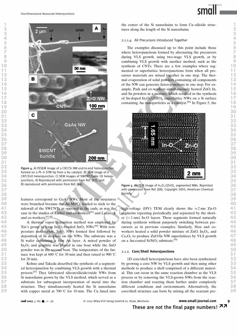
features correspond to GaAs NWs. Most of the structureswere branched because the Au MPCs tended to stick to thesidewall of the SWCNTs as opposed to the ends, as was thecase in the studies of Lieber and co-workers[82] and Lazareckand co-workers.[83,84]
A thermal vapor deposition method was employed byXieGs group to form In2O3-beaded SnO2 NWs.
[86] With tem-perature modulation, SnO2 NWs formed first followed bydeposition of In droplets on the NWs. The substrate was aSi wafer containing a thin Au layer. A mixed powder ofIn2O3 and graphite was placed in one boat while the SnOpowder was in the second boat. The temperature of the fur-nace was kept at 600 8C for 30 min and then raised to 900 8Cfor 20 min.
Kohno and Takeda described the synthesis of a segment-ed heterojunction by combining VLS growth with a thermalprocess.[87] They fabricated silicon/silicide/oxide NWs fromSi nanochains grown by the VLS method, which served as asubstrate for subsequent incorporation of metal into thestructure. They simultaneously heated the Si nanochainswith copper metal at 700 8C for 10 min. The Cu fused into
the center of the Si nanochains to form Cu–silicide struc-tures along the length of the Si nanochains.
2.1.1.4. All Precursors Introduced Together
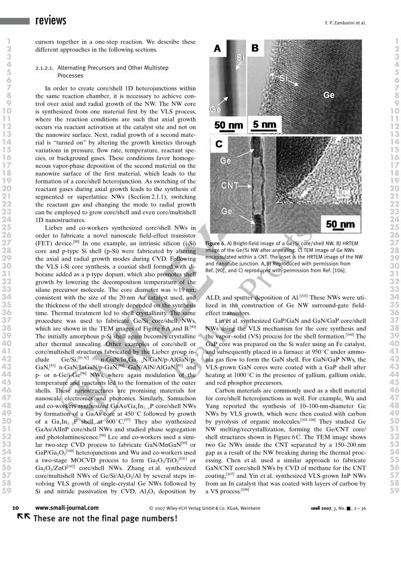
The examples discussed up to this point include thosewhere heterojunctions formed by alternating the precursorsduring VLS growth, using two-stage VLS growth, or bycombining VLS growth with another method, such as thesynthesis of CNTs. There are a few examples where seg-mented or superlattice heterojunctions form when all pre-cursor materials are mixed together in one step. The ther-mal evaporation of solid powders containing all componentsof the NW can generate heterojunctions in one step. For ex-ample, Park and co-workers simultaneously heated ZnO, In,and Sn powders in a mixture, which resulted in the synthesisof Sn-doped In2O3/ ACHTUNGTRENNUNG(ZnO)4 superlattice NWs on a Si surfacecontaining Au nanoparticles as a catalyst.[88] In Figure 5, the
high-voltage (HV) TEM clearly shows the �2 nm Zn-Osegments repeating periodically and separated by the short-er (<1 nm) In-O layers. These segments formed naturallyduring synthesis without purposely switching between pre-cursors as in previous examples. Similarly, Hou and co-workers heated a solid powder mixture of ZnO, In2O3, andCo2O3 to produce ZnO/In NW superlattices by VLS growthon a Au-coated Si/SiO2 substrate.
[89]
2.1.2. Core/Shell Heterojunctions
1D core/shell heterojunctions have also been synthesizedby growing a core NW by VLS growth and then using othermethods to produce a shell comprised of a different materi-al. This can occur in the same reaction chamber as the VLSprocess or by removing the VLS-grown NWs from the reac-tion chamber and reacting them further under completelydifferent conditions and environments. Alternatively, thecore/shell structure can form by mixing all the reactant pre-
Figure 4. A) FESEM image of a CNT/Si NW end-to-end heterojunctionformed on a Pt–Ir STM tip from a Au catalyst. B) SEM image of aCNT/ZnO heterojunction. C) SEM images of SWCNT/GaAs 1D hetero-junctions. A) Reproduced with permission from Ref. [82], andB) reproduced with permission from Ref. [84]. Figure 5. HV-TEM image of In2O3/ACHTUNGTRENNUNG(ZnO)4 segmented NWs. Reprinted
with permission from Ref. [88]. Copyright 2005, American ChemicalSociety.
small 2007, 3, No.& , 2 – 36 � 2007 Wiley-VCH Verlag GmbH&Co. KGaA, Weinheim www.small-journal.com 9
These are not the final page numbers! ��
One-Dimensional Nanoscale Heterojunctions
1 12 23 34 45 56 67 78 89 9
10 1011 1112 1213 1314 1415 1516 1617 1718 1819 1920 2021 2122 2223 2324 2425 2526 2627 2728 2829 2930 3031 3132 3233 3334 3435 3536 3637 3738 3839 3940 4041 4142 4243 4344 4445 4546 4647 4748 4849 4950 5051 5152 5253 5354 5455 5556 5657 5758 5859 59
cursors together in a one-step reaction. We describe thesedifferent approaches in the following sections.
2.1.2.1. Alternating Precursors and Other MultistepProcesses
In order to create core/shell 1D heterojunctions withinthe same reaction chamber, it is necessary to achieve con-trol over axial and radial growth of the NW. The NW coreis synthesized from one material first by the VLS process,where the reaction conditions are such that axial growthoccurs via reactant activation at the catalyst site and not onthe nanowire surface. Next, radial growth of a second mate-rial is “turned on” by altering the growth kinetics throughvariations in pressure, flow rate, temperature, reactant spe-cies, or background gases. These conditions favor homoge-neous vapor-phase deposition of the second material on thenanowire surface of the first material, which leads to theformation of a core/shell heterojunction. As switching of thereactant gases during axial growth leads to the synthesis ofsegmented or superlattice NWs (Section 2.1.1), switchingthe reactant gas and changing the mode to radial growthcan be employed to grow core/shell and even core/multishell1D nanostructures.
Lieber and co-workers synthesized core/shell NWs inorder to fabricate a novel nanoscale field-effect transistor(FET) device.[90] In one example, an intrinsic silicon (i-Si)core and p-type Si shell (p-Si) were fabricated by alteringthe axial and radial growth modes during CVD. Followingthe VLS i-Si core synthesis, a coaxial shell formed with di-borane added as a p-type dopant, which also promotes shellgrowth by lowering the decomposition temperature of thesilane precursor molecule. The core diameter was �19 nm,consistent with the size of the 20 nm Au catalyst used, andthe thickness of the shell strongly depended on the synthesistime. Thermal treatment led to shell crystallinity. The sameprocedure was used to fabricate Ge/Si core/shell NWs,which are shown in the TEM images of Figure 6A and B.[90]
The initially amorphous p-Si shell again becomes crystallineafter thermal annealing. Other examples of core/shell orcore/multishell structures fabricated by the Lieber group in-clude Ge/Si,[91, 92] n-GaN/InxGa1�xN/GaN/p-AlGaN/p-GaN,[93] n-GaN/InGaN/p-GaN,[94] GaN/AlN/AlGaN,[95] andp- or n-Ge/i-Ge[96] NWs, where again modulation of thetemperature and reactants led to the formation of the outershells. These nanostructures are promising materials fornanoscale electronics and photonics. Similarly, Samuelsonand co-workers synthesized GaAs/GaxIn1�xP core/shell NWsby formation of a GaAs core at 450 8C followed by growthof a GaxIn1�xP shell at 600 8C.[97] They also synthesizedGaAs/AlInP core/shell NWs and studied phase segregationand photoluminescence.[98] Lee and co-workers used a simi-lar two-step CVD process to fabricate GaN/MnGaN[99] orGaP/Ga2O3
[100] heterojunctions and Wu and co-workers useda two-stage MOCVD process to form Ga2O3/TiO2
[101] orGa2O3/ZnO
[102] core/shell NWs. Zhang et al. synthesizedcore/multishell NWs of Ge/Si/Al2O3/Al by several steps in-volving VLS growth of single-crystal Ge NWs followed bySi and nitride passivation by CVD, Al2O3 deposition by
ALD, and sputter deposition of Al.[103] These NWs were uti-lized in the construction of Ge NW surround-gate field-effect transistors.
Lin et al. synthesized GaP/GaN and GaN/GaP core/shellNWs using the VLS mechanism for the core synthesis andthe vapor–solid (VS) process for the shell formation.[104] TheGaP core was prepared on the Si wafer using an Fe catalyst,and subsequently placed in a furnace at 950 8C under ammo-nia gas flow to form the GaN shell. For GaN/GaP NWs, theVLS-grown GaN cores were coated with a GaP shell afterheating at 1000 8C in the presence of gallium, gallium oxide,and red phosphor precursors.
Carbon materials are commonly used as a shell materialfor core/shell heterojunctions as well. For example, Wu andYang reported the synthesis of 10–100-nm-diameter GeNWs by VLS growth, which were then coated with carbonby pyrolysis of organic molecules.[105,106] They studied GeNW melting/recrystallization, forming the Ge/CNT core/shell structures shown in Figure 6C. The TEM image showstwo Ge NWs inside the CNT separated by a 150–200 nmgap as a result of the NW breaking during the thermal proc-essing. Chen et al. used a similar approach to fabricateGaN/CNT core/shell NWs by CVD of methane for the CNTcoating,[107] and Yin et al. synthesized VLS-grown InP NWsfrom an In catalyst that was coated with layers of carbon bya VS process.[108]
Figure 6. A) Bright-field image of a Ge/Si core/shell NW. B) HRTEMimage of the Ge/Si NW after annealing. C) TEM image of Ge NWsencapsulated within a CNT. The inset is the HRTEM image of the NWand nanotube junction. A,B) Reproduced with permission fromRef. [90], and C) reproduced with permission from Ref. [106].
10 www.small-journal.com � 2007 Wiley-VCH Verlag GmbH&Co. KGaA, Weinheim small 2007, 3, No.& , 2 – 36
�� These are not the final page numbers!
reviews F. P. Zamborini et al.
1 12 23 34 45 56 67 78 89 9
10 1011 1112 1213 1314 1415 1516 1617 1718 1819 1920 2021 2122 2223 2324 2425 2526 2627 2728 2829 2930 3031 3132 3233 3334 3435 3536 3637 3738 3839 3940 4041 4142 4243 4344 4445 4546 4647 4748 4849 4950 5051 5152 5253 5354 5455 5556 5657 5758 5859 59
Zhou and co-workers grew thin shells (�10 nm) ofFe3O4 on the outside of MgO NWs formed by the VLSmechanism.[109,110] They used pulsed laser deposition (PLD)of Fe3O4 powder with growth speeds close to 2–3 Kmin
�1
after laser ablation. The same group also synthesized MgO/LaCaMnO3, MgO/LaSrMnO3,
[111] MgO/YBa2Cu3O6.66, MgO/La0.67Ca0.33MnO3, and MgO/PbZr0.58Ti0.42O3
[112] core/shell het-erostructures by combining VLS core growth and PLD shelldeposition. Bell and co-workers used the same VLS/PLDmethod to fabricate p-Si/n-CdS core/shell heterojunc-tions.[113] Boron doped p-Si NW cores were grown on an oxi-dized silicon substrate with the assistance of Au catalystsunder the flow of SiH4 and B2H6 precursors. As prepared p-Si NWs were coated immediately with an n-CdS shell usinga PLD system.
Gçsele and co-workers employed atomic layer deposi-tion (ALD) to produce uniform Al2O3 shells surroundingVLS-grown ZnO cores.[114] The ZnO NWs were synthesizedfrom zinc vapor after carbothermal reduction of ZnOpowder precursor at 910 8C. The usual thickness of the NWsranged between 10–30 nm, and the length reached up to20 mm. The shell was synthesized in the ALD chamber fromAl ACHTUNGTRENNUNG(CH3)3 and H2O precursors as sources of aluminum andoxygen, respectively. In this example the shell thickness isdirectly proportional to the number of precursor/purgecycles, as opposed to growth time. After a total number of65 cycles, the Al2O3 shell thickness was 10.0�0.3 nm. Thesame group used thermal oxidation of Si NWs under O2
flow to form Si/SiOx core/shell structures with an oscillatingdiameter of the oxide shell.[115] The first step involvedgrowth of Si NWs on a SiACHTUNGTRENNUNG(110) substrate (coated with an8 nm Au layer) from a SiO precursor at an evaporation tem-perature of 1050 8C. Once the NW growth was complete theoxide layer formed on the Si NWs was removed by chemicaletching in HF solution. Subsequent high-temperature treat-ment at 1000 8C with an O2 flow led to the formation of anoscillating SiO2 shell on the Si NW cores. The average NWdiameter ranged from 60 to 90 nm and the length was onthe order of micrometers.
2.1.2.2. All Precursors Introduced Together
Most methods for forming 1D core/shell heterojunctionsby VLS require a second step to produce a shell over theVLS-grown core wire. However, there are VLS methodswhere all the precursors for the core and the shell are intro-duced to the growth chamber at the same time. This one-step VLS process is used to produce the core and shell si-multaneously, which occurs due to differences in the reactiv-ity of the core and shell material. An excellent example isthe work of Hsu and Lu for the fabrication of CdS/ZnScore/shell heterojunctions.[116] They fed CdS (CdACHTUNGTRENNUNG(S2CN-ACHTUNGTRENNUNG(C3H7)2)2 denoted as Cd33) and ZnS ([ZnACHTUNGTRENNUNG(S2CNBu2)2]2 de-noted as Zn44) precursors into the system simultaneously.Cd33 decomposes at the catalyst first since it is of higher re-activity than Zn44, leading to growth of the CdS core viathe VLS mechanism. The CdS core subsequently serves as acatalyst for thermal decomposition of Zn44, resulting in thecore/shell heterojunctions. Hsu et al. used a similar proce-
dure, introducing all precursors in a single step, to synthe-size CdS/ZnS and Cd1�xZnxS/ZnS coaxial heterojunc-tions.[117] Heo et al. synthesized ZnO/ ACHTUNGTRENNUNG(Mg,Zn)O radial NWsspontaneously, where the core grows by the VLS mechanismand the composition is determined by bulk solid solubili-ty.[118,119] The (Mg, Zn)O shell grows as a heteroepitaxiallayer. Jang et al. used a one-step thermal CVD reaction ofGaP, B2O3, and NH3 to synthesize GaN/BN core/shell nano-cables.[120] Gwo and co-workers fabricated In/GaN core/shellNWs on a substrate containing Au catalyst by a single evap-oration step.[121] Lee and co-workers synthesized Ge/SiOx
coaxial nanocables by an oxide-assisted self-catalyzed VLSprocess.[122] A reaction occurs within the droplet of GeO4/SiO2 to form the SiOx shell while the core consists of Ge.Other examples of single-step syntheses include core/shellheterojunctions of GaN/BN NRs,[123] linear or helical SiC/SiOx NWs,
[124–126] ZnS/SiO2 NWs (ZnS wrapped in high-den-sity SiO2),
[127] and GaP/C and GaP/SiOx/C nanocables.[128]
Seo et al. synthesized GaN NWs coated with boron car-bonitride (BCN) layers when Ga, Ga2O3, CNTs, B2O3, andNH3 precursors were introduced into the reaction chamberat the same time.[129] The high-temperature processing led tothe formation of the Ga core that grew by the VLS mecha-nism on the Fe catalyst, coated with BCN layers. Wanget al. fabricated Cu/SiO2�x NWs by encapsulating Cu nano-particles inside the SiO2�x NW.
[130] The procedure involvedsimultaneous heating of the precursor powder mixture ofSiO and CuO. Under the presence of H2 in the atmospherethe environment is suitable for reducing the CuO to Cu par-ticles and formation of SiO2�x NW/Cu NP heterostructures.Wu et al. reported a VLS process to form B NWs on a sub-strate containing Au catalyst.[131] The diameter ranged from30 to 500 nm and the length reached hundreds of microme-ters. Evaporation of SiOx during B NW growth led to bead-like B/SiOx heterojunctions. The VLS growth mechanismwas also proposed for the core in SiC/BN or Si3N4/BN core/shell NWs synthesized by Tang and co-workers.[132, 133] Theheterostructures were synthesized on Ni-supported highlyordered pyrolytic graphite (HOPG) and Ni–BN substratesfrom B and SiO2 precursors either under the flow of nitro-gen and argon for HOPG or ammonia and argon for theBN substrate. Zhou et al. synthesized b-SiC/SiOx by a one-step procedure.[134, 135] A tablet of silicon and graphite pow-ders was reacted with atomic hydrogen activated at 2200 8C,leading to the formation of SiHx and CHx precursors. The b-SiC NWs formed by the VLS process where metallic parti-cle impurities served as the catalyst. The SiC NWs werecoated with an amorphous �1–2-nm-thick SiOx shell.
2.2. Vapor–Solid (VS) and Catalyst-Free Growth Mecha-nisms
There are a large number of reports of heterojunctionssynthesized without using any catalyst to promote thegrowth of nanostructures. The growth mechanism is oftenclassified as a vapor–solid (VS) process, but usually is notwell understood. We will review heterojunctions formed bythe VS method and other growth procedures not requiring a
small 2007, 3, No.& , 2 – 36 � 2007 Wiley-VCH Verlag GmbH&Co. KGaA, Weinheim www.small-journal.com 11
These are not the final page numbers! ��
One-Dimensional Nanoscale Heterojunctions
1 12 23 34 45 56 67 78 89 9
10 1011 1112 1213 1314 1415 1516 1617 1718 1819 1920 2021 2122 2223 2324 2425 2526 2627 2728 2829 2930 3031 3132 3233 3334 3435 3536 3637 3738 3839 3940 4041 4142 4243 4344 4445 4546 4647 4748 4849 4950 5051 5152 5253 5354 5455 5556 5657 5758 5859 59
catalyst in the next sections. The sections are divided by thestructures formed, including segmented, core/shell, orbranched heterojunctions. We also divided the sections intothose using an alternating flow of precursors or reactionsconditions, those using a combination of techniques, andthose where all of the reactants are combined together. It isimportant to note that even in examples where all of the re-actants are combined, multiple reaction steps may occur toform the heterojunction.
2.2.1. Segmented Heterojunctions
2.2.1.1. Alternating Flow of Precursors
Chung and co-workers fabricated segmented GaN nano-wire p–n junctions via hydride vapor-phase epitaxy (HVPE)using an alternating flow of precursors to form the differentsegments.[136] A GaCl precursor was produced via the reac-tion of HCl gas and Ga metal and mixed with NH3 to growGaN at 478 8C. The n-type segment of the NW forms duringthe nitrogen flow while the p-doped region grows by intro-ducing Cp2Mg to the growth chamber. The �3-mm-long p–nGaN NWs are promising for use as diodes in electronic andphotonic devices.
2.2.1.2. All Precursors Combined Together
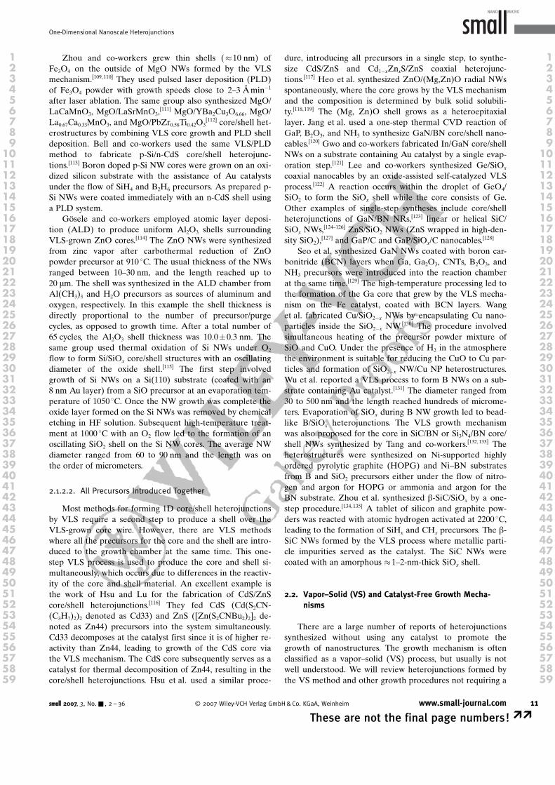
Golberg and co-workers used thermal evaporation of amixture of precursor powders to fabricate Ga/ZnS segment-ed nanowires encapsulated within a silica tube, as shown inFigure 7.[137] A mixture of ZnS, Ga2O3, and SiO powders
was heated at 1400–1500 8C. Even though all of the precur-sors are mixed together, they proposed two stages ofgrowth, where silica tubes formed first by oxide-assistedgrowth and served as templates for the following NW heter-ojunction synthesis. An increase in temperature allows forthe deposition of Ga/ZnS solution inside the tube, and aftersupersaturation, ZnS precipitates to form a separate seg-ment of the NW. The typical diameter of the Ga/ZnS heter-ojunction ranges between 150–250 nm and the thickness ofthe silica tube is 4–8 nm. Other heterojunctions synthesizedby the same group include ZnS-sheathed Zn/Cd NWsformed in a one-step thermal process.[138] Rapid heating of aZnS and CdS powder mixture to 1200 8C led to the forma-tion of 30–70-nm-diameter Zn/Cd segmented NWs encapsu-
lated with a few-nanometers-thick ZnS shell on the walls ofthe quartz tube. The same group also used thermal evapora-tion of a solid mixture of In and SiO precursors to prepareIn/Si segemented NWs sheathed with amorphous silica.[139]
The Si NWs sheathed with silica grow by oxide-assistedgrowth, while silica nanotubes grow in the opposite direc-tion at the junction between the Si NWs and In droplets.Vapor-phase In is drawn into the silica nanotubes and con-denses to form the final In/Si segmented junctions sheathedwith amorphous silica. Wang et al. synthesized bundles orbrushlike arrays of Si/SiOx nanostructures formed by pyroly-sis of a Si and SiOx powder mixture.
[140]
2.2.2. Core/Shell Heterojunctions
2.2.2.1. Alternating Reaction Precursors or Conditions
Fukui and co-workers synthesized various core/shell het-erojunctions by selective-area (SA)-MOVPE, where theprecursors were introduced in an alternating fashion.[141–144]
For example, they synthesized GaAs/AlGaAs[143,144] hexago-nal pillars and InP/InAs[142] core/shell structures in thismanner. In the case of InP/InAs, they grew the InP corefirst at 635 8C from trimethylindium (TMI) and tertiarybu-tylphosphine (TBP) precursors followed by growth of theshell from TMI and AsH3 precursors at 400 8C. They used asimilar method to prepare InP/InAs/InP core/multishell het-erojunctions on a hexagonally patterned surface.[141] In thiscase they formed the InP/InAs core/shell structure as previ-ously described and then added another InP shell by con-trolling the growth temperature (600 8C) as well as the parti-al pressure of the TBP precursor. Figure 8A shows an SEMimage of the highly aligned core/multishell NW arrays.[141]
The shape of the pattern from the substrate was transferredto the grown nanostructures, which have a hexagonal crosssection as shown for the individual NW in Figure 8B. Addi-tionally, this image reveals the composition of the NW withwell-defined regions of the InP core and InAs/InP shells.The length of this core/multishell heterostructure was2.5 mm and the diameter of the InP core was 70 nm, whilethe thickness of the InAs and InP shell was 5 nm and30 nm, respectively. Yi and co-workers also used MOVPEand alternating reaction conditions to fabricate ZnO/Mg0.2Zn0.8O
[145,146] and ZnO/GaN[147] core/shell structures.Zhan and co-workers heated a powder mixture of SiO
and ZnS or SiO and ZnSe to 1300 8C for 1 h and then to1600 8C or 1500 8C for 1.5 h to form 60–120-nm-diameter Si/ZnS biaxial and ZnS/Si/ZnS triaxial NWs or 40–90-nm-di-ameter Si/ZnSe biaxial NWs through a two-stage thermal-evaporation process.[148] The NWs were several micrometersin length. Chen and co-workers used a two-step procedureto form ZnO/ZnGa2O4 core/shell heterojunctions.
[149] TheZnO NWs, formed by a thermal vapor deposition process,served as templates for the shell deposition. The Ga2O3 andgraphite powders (shell precursors) were placed in a zone ofthe furnace held at 1000 8C, while the ZnO NWs wereplaced downstream. The deposition temperature was 600–900 8C. Similarly, Hu et al. synthesized ZnS/Si core/shellNWs.[150] They synthesized ZnS NWs first by heating ZnS
Figure 7. TEM image of a Ga/ZnS segmented NW within a silica shell.Reproduced with permission from Ref. [137].
12 www.small-journal.com � 2007 Wiley-VCH Verlag GmbH&Co. KGaA, Weinheim small 2007, 3, No.& , 2 – 36
�� These are not the final page numbers!
reviews F. P. Zamborini et al.
1 12 23 34 45 56 67 78 89 9
10 1011 1112 1213 1314 1415 1516 1617 1718 1819 1920 2021 2122 2223 2324 2425 2526 2627 2728 2829 2930 3031 3132 3233 3334 3435 3536 3637 3738 3839 3940 4041 4142 4243 4344 4445 4546 4647 4748 4849 4950 5051 5152 5253 5354 5455 5556 5657 5758 5859 59

powder at 1200 8C and used these NWs as a template forthe growth of the Si shell, which formed after heating SiOpowder at 1450 8C for 1 h. Zhu et al. reported ZnS nano-structures coated with a BN layer.[151] The ZnS twinned-crystal whiskers were prepared first by heating the ZnSpowder at 1200 8C under N2, and then reheated again withB/N/O vapors under N2/NH3 flow. Zheng and co-workerssynthesized tetrapod ZnO NRs coated with a SnO2 sheathby a two-step procedure involving the initial formation ofZnO nanostructures through heating of a zinc powder at800 8C, and subsequent reheating to 770 8C with the intro-duction of a SnH4/N2 mixture to form the final ZnO/SnO2
core/shell heterojunctions.[152]
Yin et al. reported the synthesis of several-micrometer-long cubic aluminum nitride/boron nitride (c-AlN/BN) co-axial nanotubes by the VS method.[153] The AlCl3 and B/N/O precursors were heated in the furnace under Ar flow.When the temperature reached 950 8C, they introduced aflow of NH3/N2 only and raised the temperature to 1200 8Cfor 1.2 h. The temperature was then increased further to1600 8C. AlN nanotubes grow first at the lower temperaturefollowed by the BN shell, which forms at higher tempera-tures. The outer diameter of the heterojunctions was�50 nm with a wall thickness of about 15 nm and a BNcoating of 2–3 nm. Golberg and co-workers synthesized ZnSor Si/SiO2 NWs sheathed with BN coatings.[154] For thelatter, SiO precursors were placed above B/N/O precursors.Heating at 1200 8C led to the formation of Si/SiO2 NWs andchanging to 1600 8C and a flow of N2/NH3 led to growth of
the BN coating. ZnS/BN core/shell NWs were prepared sim-ilarly. Alternatively, the Si/SiO2 or ZnS NWs were preparedfirst and then subsequently coated with BN. More recently,the same group synthesized BN nanosheets protruding formSi3N4 NWs by placing a BN crucible containing Si powderabove a crucible containing the B/N/O precursor and B2O3
powder in a graphite susceptor, which was heated at 1500 8Cin N2 and 1750 8C in N2/NH3 to form the Si3N4 NWs and BNsheets, respectively.[155]
Golberg and co-workers used a VS route in a CVDsystem to produce Mg2Zn11/MgO beltlike nanocables byheating Mg and ZnO powders.[156] The ZnO and Mg pow-ders were heated to temperatures of 1300–1400 8C and 800–900 8C, respectively. The Mg2Zn11/MgO nanocables were col-lected from the graphite surface inside the furnace. Thecables were typically 30–150 nm wide and tens of microme-ters in length. Another example is the synthesis of Zn/ZnOcore/shell heterostructures by thermal reduction of ZnOwith H2 to form the Zn core and thermal annealing to formthe ZnO shell.[157]
2.2.2.2. All Precursors Mixed Together
Li and co-workers used thermal evaporation to fabricateZnSe nanopeas filled inside SiO2 nanotubes by a one-stepthermochemical method.[158] Two separate mixtures of pre-cursor powders containing Se with Zn and Si with SiO2
were placed in the furnace and heated to 1300 8C for 2 hunder Ar flow. The products were collected on a Si wafer.The core/shell structure was �80 nm in diameter and tensof micrometers in length. The nanotube wall was about 20–25 nm thick and ZnSe-formed nanodots or short rods wereobserved inside the nanotube&&sentence ok?&&. Hsuet al. synthesized ZnO/ZnGa2O4 NWs by heating the pre-cursor mixture of Zn metal and Ga powder at 600 8C for1 h.[159]
Peng and co-workers synthesized core/shell structuresfrom precursors placed in different temperature zones.[160] Inthis example, they synthesized CdSe-filled silica nanotubesby loading Si and SiO2 powders in the center of a furnace,with Cd and Se precursors upstream and the collection sub-strate downstream. The furnace was set to 1200 8C, whichcaused the Si and SiO2 powders to be at 1200 8C, the Cd andSe to be at 900 8C, and the substrate (where CdSe/silica het-erostructrues were collected) at 1100 8C. In another exam-ple, Hu et al. synthesized partially Ga-filled Ga2O3/ZnOcore/shell coaxial nanotubes by simultaneous heating Ga2O3
and ZnO precursors at 1350 8C for 2 h.[161] The core/shellnanostructures were tens of micrometers long and 150 nm indiameter with a shell-wall thickness of 40 nm and an innercore of �80 nm. Uemura and co-workers fabricated InS/SiO2 core/shell NWs 30–200 nm in diameter and tens of mi-crometers in length by a one-step physical vapor-depositionprocess.[162] InS and silicon powders were heated to 900–1000 8C for 1 h and the product collected from the wall ofthe alumina crucible. Teo et al. prepared Si/SiO2 core/shellNWs on a zeolite template where the diameter of the Sicore varied between 1–5 nm and the SiO2 shell was about20–40-nm thick.[163] The SiO powder was used as a precursor
Figure 8. A) SEM image of aligned InP/InAs/InP core/shell/shell NWs.B) SEM image of the cross section of an InP/InAs/InP NW showinghexagonal shape and composition. Reprinted with permission fromRef. [141]. Copyright 2006, American Institute of Physics.
small 2007, 3, No.& , 2 – 36 � 2007 Wiley-VCH Verlag GmbH&Co. KGaA, Weinheim www.small-journal.com 13
These are not the final page numbers! ��
One-Dimensional Nanoscale Heterojunctions
1 12 23 34 45 56 67 78 89 9
10 1011 1112 1213 1314 1415 1516 1617 1718 1819 1920 2021 2122 2223 2324 2425 2526 2627 2728 2829 2930 3031 3132 3233 3334 3435 3536 3637 3738 3839 3940 4041 4142 4243 4344 4445 4546 4647 4748 4849 4950 5051 5152 5253 5354 5455 5556 5657 5758 5859 59
and heated gradually to 1250 8C and held at this tempera-ture for 1 h. The product was collected from the zeolite sub-strate. During this procedure they also fabricated siliconnanotubes filled with amorphous silica and biaxial silicon/silica NWs. Wang et al. synthesized ZnSe/Si bi-coaxial NWsthat were 80–100 nm in diameter and tens of micrometerslong by thermal evaporation of a ZnSe powder at 1250 8Cfor 2 h under Ar/H2 flow (5% H2).
[164] Li and Wang report-ed a single-step thermal evaporation to form single-crystal-line Si/CdSe nanocables.[165] The CdSe was heated to1200 8C for 2 h and the product collected at a silicon wafercoated with a thin oxide layer.
Thermal evaporation of a MoSi2 precursor led to the for-mation of �100-nm-diameter Si/SiOx core/shell NWs, whichwere several micrometer long.[166] Li and Jiao produced Au/Si junctions in Si/SiOx core/shell NWs by filling Au into thevoids between the Si core and the SiOx shell.
[167] Smashed Siwafers were used as precursors and alumina (0001) with athin Au film as a substrate. Subsequently, the furnace washeated at 1300 8C for 2–4 h under an Ar/H2 flow (10% H2).
Other examples include CaF2/a-C and MgF2/a-C core/shell NWs (a-C=amorphous carbon) reported by Chiu andco-workers.[168] The precursors, which include CaC2 andMg2N3, were reacted with C6F6 at elevated temperatures toproduce CaC2/a-C and Mg2F2/a-C, respectively. Wang andco-workers synthesized Zn/ZnO core/shell nanobelts andnanotubes by evaporating ZnO powder at 1350 8C and intro-ducing an Ar flow for 30 min.[169,170] The products were col-lected at a silicon substrate placed in the 200–400 8C temper-ature region. Kang and co-workers fabricated Zn/ZnSiO4
nanocables by vapor-phase oxidation of Zn powder.[171] TheZn powder was heated up to 1100 8C at a rate of 15 8Cmin�1
under N2 flow and the product collected at a Si substrate.The nanocables were �100 nm in diameter with a �25-nm-thick shell.
2.2.2.3. Combined Techniques
Catalyst-free vapor methods can be combined withother methods to grow various heterojunctions. Solution-based systems are commonly used as the second technique.Jiang et al. used this setup to prepare FeCoNi/SiOx core/shell NWs.[172] First, SiOx NWs were synthesized by heatinga mixture of Si and SiO2 powder and collecting the producton an Al2O3 substrate. Then, the Al2O3 substrate containingSiOx NWs was placed in a solution of FeCoNi vitriol. Con-tinued growth of SiOx on the Al2O3 substrate led to NWswith a crystalline metallic FeCoNi alloy core (�20 nm in di-ameter) surrounded by a double-layer amorphous SiOx
shell. The typical diameter of these heterojunctions wasabout 20 nm for the FeCoNi core, 50 nm for the inner shell,and 90 nm for the outer SiOx shell layer. Similarly, a combi-nation of vapor and solution techniques was employed byFan and co-workers to fabricate ZnO/ZnS core/shellNWs.[173] ZnO NWs were initially synthesized by a vapor-phase transport process and then coated with ZnS by solu-tion self-assembly. The first solution contained Na2S and thesecond contained Zn ACHTUNGTRENNUNG(NO3)2 where the NWs were soakedfor 2 h at 60 8C. The ZnO/ZnS heterojunctions were
�100 nm in diameter and �3 mm long. Zheng and co-work-ers fabricated Se/Ag2Se nanocables;[174] they modified SeNRs, synthesized via laser ablation of a Se powder, by im-mersing them in a AgNO3 solution. The diameter of the Se/Ag2Se nanocables was �20 nm for the core and �33 nm forthe shell. Zettl and co-workers formed KI/BN, KCl/BN, andKBr/BN core/shell heterostructures by filling in BN nano-tubes (formed by substitution of C atoms in a boron oxide/nitrogen vapor phase reaction) with potassium halide crys-tals from solution by capillary action.[175] Yang et al. de-scribed another example of combining noncatalyst vapormethods with solution methods in the formation of Cu2S/Xcore/shell NW heterojunctions (X=nanoparticles of CdS,Au, or polypyrrole).[176] Cu2S NW arrays were fabricatedfirst by subjecting a Cu foil to a flow of O2 and H2S for10 h. The Cu2S NWs were subsequently coated chemicallywith nanoparticles of CdS, Au, or polypyrrole. The Cu2SNWs were 60–100 nm thick and several micrometers long,while the sheath was 20–50 nm thick.
2.2.3. Branched Heterojunctions
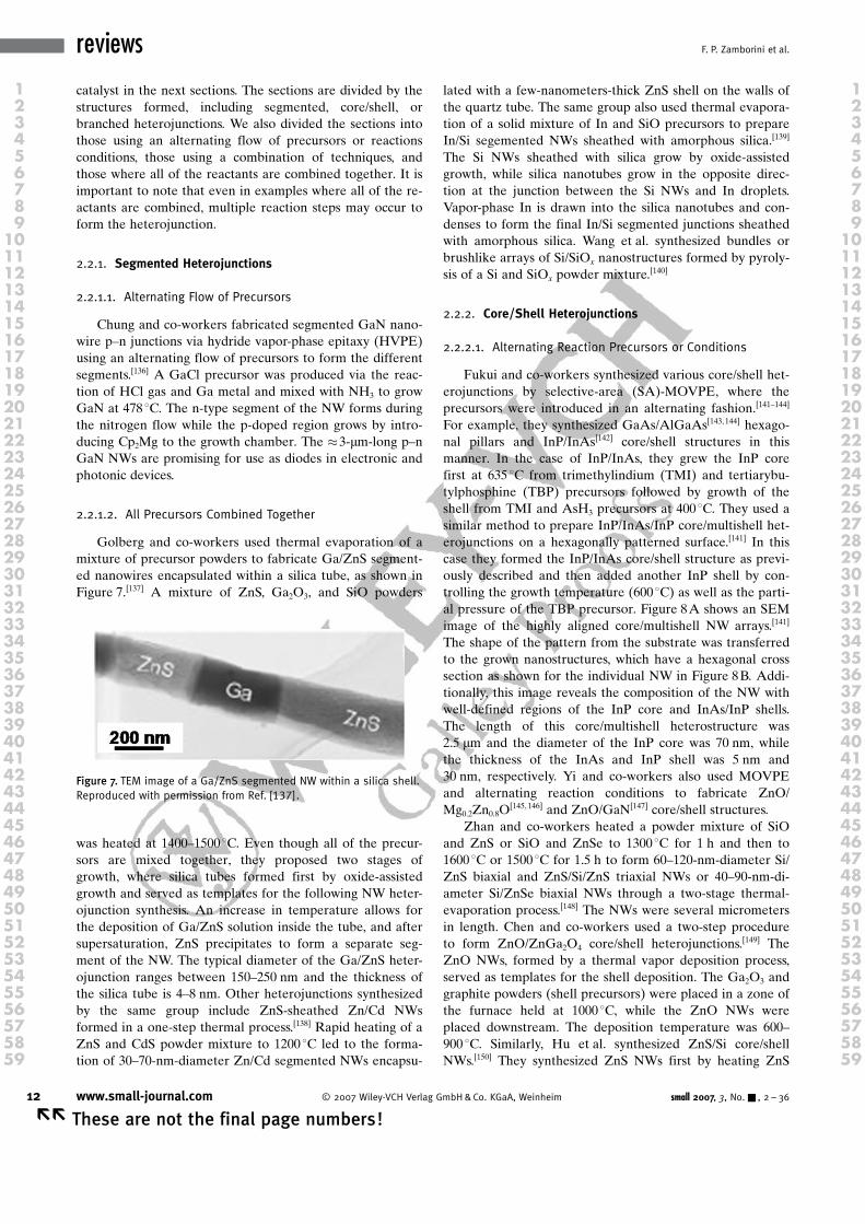
There are not many reports of branched heterojunctionsby non-catalyst methods. One example is the saw-like nano-structures synthesized by Shen et al. in a two-step VSgrowth process, where a ZnO nanobelt was synthesized firstand ZnS NWs were grown on the nanobelts.[177] Zn and SnSpowders were placed in two different zones of the furnaceand heated to 550 8C in 20 min. Subsequently the tempera-ture of the SnS precursor was up to 1100 8C while the Znpowder was held at 550 8C for 30 min. This resulted in theformation of an interesting saw-shape morphology as shownin Figure 9. The surface of the ZnO nanobelt remains chem-
ically active to facilitate the formation of ZnS NWs duringthe second step of the synthesis. Typically the diameter ofthe saw was about 100 nm and the length reached hundredsof micrometers.
Figure 9. TEM image of a sawlike heterojunciton of ZnS NWs grownon a ZnO belt. Reprinted with permission from Ref. [177]. Copyright2006, American Chemical Society.
14 www.small-journal.com � 2007 Wiley-VCH Verlag GmbH&Co. KGaA, Weinheim small 2007, 3, No.& , 2 – 36
�� These are not the final page numbers!
reviews F. P. Zamborini et al.
1 12 23 34 45 56 67 78 89 9
10 1011 1112 1213 1314 1415 1516 1617 1718 1819 1920 2021 2122 2223 2324 2425 2526 2627 2728 2829 2930 3031 3132 3233 3334 3435 3536 3637 3738 3839 3940 4041 4142 4243 4344 4445 4546 4647 4748 4849 4950 5051 5152 5253 5354 5455 5556 5657 5758 5859 59
2.3. Carbon-Containing Heterojunctions
We have already described heterojunctions containingcarbon involving VLS growth where 1) a NW is synthesizedby VLS and then a carbon shell is deposited onto it to forma core/shell heterojunction or 2) a CNT is first synthesizedand a NW grown from a catalyst bound to the CNT by VLSto form a segmented or branched heterojunction. In thissection, we describe other types of segmented or core/shellheterojunctions containing carbon species such as CNTs,SiC, CNx, amorphous carbon, or diamond synthesizedmostly by multi-step procedures.
2.3.1. Segmented Heterojunctions
Golberg and co-workers prepared segmented SiC/CNTnanochains after thermal treatment of SiC/SiO2/CNT core/shell nanocables.[178] Thermal evaporation of SiO and Fepowders under a CH4 atmosphere led to the formation ofSiC/SiO2/CNT nanocables with diameters between 20–50 nm and lengths of several micrometers. High-tempera-ture annealing in vacuum transformed the nanocables intoSiC/CNT end-to-end nanochains. Wu and co-workers report-ed the synthesis of segmented CNx/CNT heterojunctions byCVD through pyrolysis of a mixture of ferrocene and mela-mine.[179, 180] Similarly, Hu et al. fabricated CNx/C nanotubejunctions by pyrolysis of iron phthalocyanine, where C seg-ments were obtained with an H2 flow only and CNx with anNH3 carrier gas.
[181] The diameter ranged between 30–60 nmand the length reached tens of micrometers. Ma and Wangsynthesized segmented heterojunctions between CNx nano-tubes and CNTs by a two-step microwave plasma-assistedCVD process using an Fe catalyst, where N2/CH4 and H2/CH4 gaseous mixtures formed the CNx and CNTs, respec-tively.[182] Cassel et al. prepared end-to-end junctions consist-ing of vertical connections between two MWCNTs by atwo-step process.[183] In the first step, they grew verticallyaligned CNTs and embedded them into an SiO2 matrix. Inthe second step, they electroplated Ni on the end of the firstCNTs and grew the second segment of CNTs by a plasma-enhanced CVD process. Multiple segments could be formedby repeating the procedure. The first generation of CNTswas about 50 nm in diameter and the second was also�50 nm at the junction point but became thinner towardsthe end. The average length was about 1 mm. Also, Liu et al.synthesized CNT/ZnO heterojunction arrays by pyrolysis ofC2H2 on a zinc foil at 850 8C under combined Ar and H2
flow passed through a water bubbler.[184] Zn served as thesource of ZnO and catalyst for CNT growth by the tip-growth mechanism while the water enhanced CNT growthand promoted ZnO formation. Post-synthesis annealing ofthe sample under Ar passed through the water bubbler ledto increased growth of the ZnO structures formed at the tipof the CNTs.[184] The flow rate of Ar during synthesis con-trolled the formation of ZnO nanoparticles or ZnO nano-rods, with the latter occurring at higher flow rates.
2.3.2. Core/Shell Heterojunctions
The synthesis of core/shell heterojunctions with carbonusually involves either 1) filling a carbon nanotube withsome material, 2) coating a carbon nanotube with some ma-terial, or 3) coating a 1D material with a carbon shell. Thereare also examples of carbon-containing materials in the coreor shell by various methods. In the first example, Chan et al.fabricated multi-walled carbon nanotubes (MWCNTs) filledwith Pd using a microwave plasma-enhanced CVD systemin a two-step process.[185] A Pd film was activated by a H2
plasma and then methane and H2 were introduced into thereaction chamber, resulting in core/shell Pd-filled CNTswith some void spaces between the Pd regions.
Examples of the second procedure include heterojunc-tions of MWCNT/maghemite composites made by Zhangand co-workers.[186] MWCNTs, made by catalytic decomposi-tion of methane, were coated with iron oxides using high-temperature decomposition of ferrocene. Also, Strongin andco-workers synthesized MWCNTs or BNTs by arc-dischargeand a CNT substitution reaction, respectively, and coatedthem with amorphous Ge that crystallized at elevated tem-perature to form MWCNT/Ge and BNT/Ge core/shell struc-tures.[187] The thickness of the Ge coating was typically 4 nmfor CNTs and 2 nm for BNTs. Duan and co-workers report-ed CNT/SiOx core/shell structures where CVD-grownMWCNTs on a silicon wafer were used as substrates.[188]
The sample was loaded into a PECVD chamber and heatedto 700 8C in the presence of hydrogen. Zhang and Dai syn-thesized SWCNT/M (where M=Au, Pd, Fe, Al, and Pb) byusing CVD to grow suspended SWCNTs over holes on aTEM grid and depositing the appropriate metal on thetubes by electron-beam evaporation.[189] The procedure re-quires deposition of a 1 nm titanium layer on the SWCNTsfor forming continuous metal wires.
Carbon also serves as a coating material by variousmethods. For example, Cao et al. formed Au NWs coatedwith an amorphous carbon shell using a plasma-assistedmethod.[190] They coated template-synthesized Au NWs dis-persed in a radio-frequency Ar plasma with a C shell usingisopropanol as a carbon source. Sun et al. used a hydrogenplasma to transform CNTs into diamond NRs.[191] The finalproduct consisted of diamond NRs coated with an amor-phous carbon sheath. The typical diameter of the diamondNRs ranged between 4–8 nm and their length reached sever-al hundreds of nanometers. Golberg and co-workers fabri-cated C/AlN/C coaxial nanotubes via substitution and car-bonitridation processes where the C atoms of CNTs werereplaced by AlN components.[192] The MWCNTs weremixed with Al2O3 powder and heated at 1600 8C for 1 hunder Ar flow and another hour under NH3 flow. The prod-uct consisted of AlN nanotubes with inner and outer layerscoated with carbon. The thickness of the carbon coating was2–2.5 nm, the tube-wall thickness was about 13 nm, and thetotal diameter ranged between 50–55 nm. Chen et al. used aCVD system to remove Si from SiC whiskers and fabricateSiC/C core/shell heterojunctions.[193] SiC whiskers wereheated to an appropriate temperature before introducingthe Cl2:H2 extraction mixture.
small 2007, 3, No.& , 2 – 36 � 2007 Wiley-VCH Verlag GmbH&Co. KGaA, Weinheim www.small-journal.com 15
These are not the final page numbers! ��
One-Dimensional Nanoscale Heterojunctions
1 12 23 34 45 56 67 78 89 9
10 1011 1112 1213 1314 1415 1516 1617 1718 1819 1920 2021 2122 2223 2324 2425 2526 2627 2728 2829 2930 3031 3132 3233 3334 3435 3536 3637 3738 3839 3940 4041 4142 4243 4344 4445 4546 4647 4748 4849 4950 5051 5152 5253 5354 5455 5556 5657 5758 5859 59
There are a few other examples of heterojunctions in-volving carbon-containing materials in the core, such as SiC/BN[194] and SiC/SiOx
[195] heterojunctions. In the former, SiC/BN core/shell structures were synthesized by mixing Si andIn2O3 in a BN crucible and heating to 1600 8C in the pres-ence of CH4 gas. The 30–60-nm-thick SiC core was coatedwith 8–15-nm-thick BN nanotubes in this single-step pro-cess. Interestingly, a 10–15 nm gap existed between the coreand the sheath. The decomposition of SiO&&SiO2?&&
onto MWCNT templates resulted in the formation of biaxialSiC/SiOx NWs as reported by Sun et al.
[195] Wang et al. syn-thesized the same SiC/SiOx biaxial NWs by reacting amor-phous SiO &&SiO2?&&with carbon/graphite at1500 8C.[196]
3. Solution-Phase Methods
3.1. Chemical Methods
In this section we describe chemical methods in the solu-tion phase or methods combining solution-phase synthesiswith some other technique, such as CNT synthesis or VLSgrowth. The chemical methods may involve the crystalliza-tion of solution-phase precursors through spontaneous oxi-dation/reduction or other chemical reactions either at roomtemperature or elevated temperatures. This usually occursin the presence of a stabilizing ligand, polymer, or surfac-tant. Some of the examples in this section involve chemicalformation of a thin film from the solution phase onto a 1Dnanostructure synthesized in solution or by some other tech-nique.
3.1.1. Branched and Segmented Heterojunctions
3.1.1.1. Alternating Solution Precursors
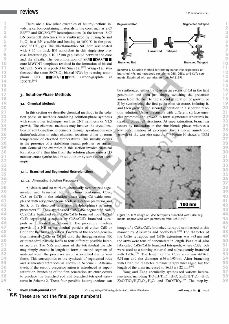
Alivisatos and co-workers chemically synthesized sege-mented and branched heterojunctions containing CdSe,CdS, or CdTe in the solution phase using Cd oxide com-plexed with alkylphosphonic acids as a cation precursor andSe, S, or Te dissolved in a tri(n-alkylphosphine) as anionprecursors.[197] They synthesized CdS/CdSe segmented rods,CdS/CdTe branched rods, CdSe/CdTe branched rods, CdSe/CdTe segmented tetrapods, or CdSe/CdTe branched tetra-pods as illustrated in Scheme 2. The procedure involvesgrowth of a NR or tetrahedral particle of either CdS orCdSe for the first generation. Growth of the second-genera-tion material (CdSe or CdTe) onto the first-generation NRor tetrahedral particle leads to four different possible heter-ostructures. The NRs and arms of the tetrahedral particlemay simply extend in length to form a second segment ofmaterial when the precursor anion is switched during syn-thesis. This corresponds to the synthesis of segmented rodsand segmented tetrapods as shown in Scheme 2. Alterna-tively, if the second precursor anion is introduced at super-saturation, branching of the first-generation structure occursto produce the branched rod and branched tetrapod struc-tures in Scheme 2. These four possible heterojunctions can
be synthesized either by 1) using an excess of Cd in the firstgeneration and then just simply switching the precursoranion from the first to the second generation of growth, or2) by synthesizing the first-generation structure, isolating it,and then growing the second generation in a separate reac-tion solution. Using precursors with different surface ener-gies promotes end growth to form segmented structures in-stead of core/shell structures. At supersaturation, branchingoccurs by nucleation in the zinc blende phase, whereas alow concentration of precursor favors linear anisotropicgrowth of the wurtzite stucture.[197] Figure 10 shows a TEM
image of a CdSe/CdTe branched tetrapod synthesized in thismanner by Alivisatos and co-workers.[197] The diameter ofthe CdSe tetrapods and CdTe extensions was �3 nm andthe arms were tens of nanometers in length. Peng et al. alsofabricated CdSe/CdTe branched tetrapods, where CdSe rodswere used as a starting material and subsequently branchedwith CdTe.[198] The length of the CdSe rods was 49.76�9.51 nm and the diameter 6.36�0.93 nm. After branchingwith CdTe the diameter remains largely unchanged but thelength of the arms increased to 86.35�9.22 nm.[198]
Yang and Zeng chemically synthesized various hetero-junctions, including TiO2/H2Ti5O11·H2O, ZnO/H2Ti5O11·H2O,ZnO/TiO2/H2Ti5O11·H2O, and ZnO/TiO2.
[199] The step-by-
Scheme 2. Solution method for forming nanoscale segmented orbranched NRs and tetrapods containing CdS, CdSe, and CdTe seg-ments. Reprinted with permission from Ref. [197].
Figure 10. TEM image of CdSe tetrapods branched with CdTe seg-ments. Reproduced with permission from Ref. [197].
16 www.small-journal.com � 2007 Wiley-VCH Verlag GmbH&Co. KGaA, Weinheim small 2007, 3, No.& , 2 – 36
�� These are not the final page numbers!
reviews F. P. Zamborini et al.
1 12 23 34 45 56 67 78 89 9
10 1011 1112 1213 1314 1415 1516 1617 1718 1819 1920 2021 2122 2223 2324 2425 2526 2627 2728 2829 2930 3031 3132 3233 3334 3435 3536 3637 3738 3839 3940 4041 4142 4243 4344 4445 4546 4647 4748 4849 4950 5051 5152 5253 5354 5455 5556 5657 5758 5859 59
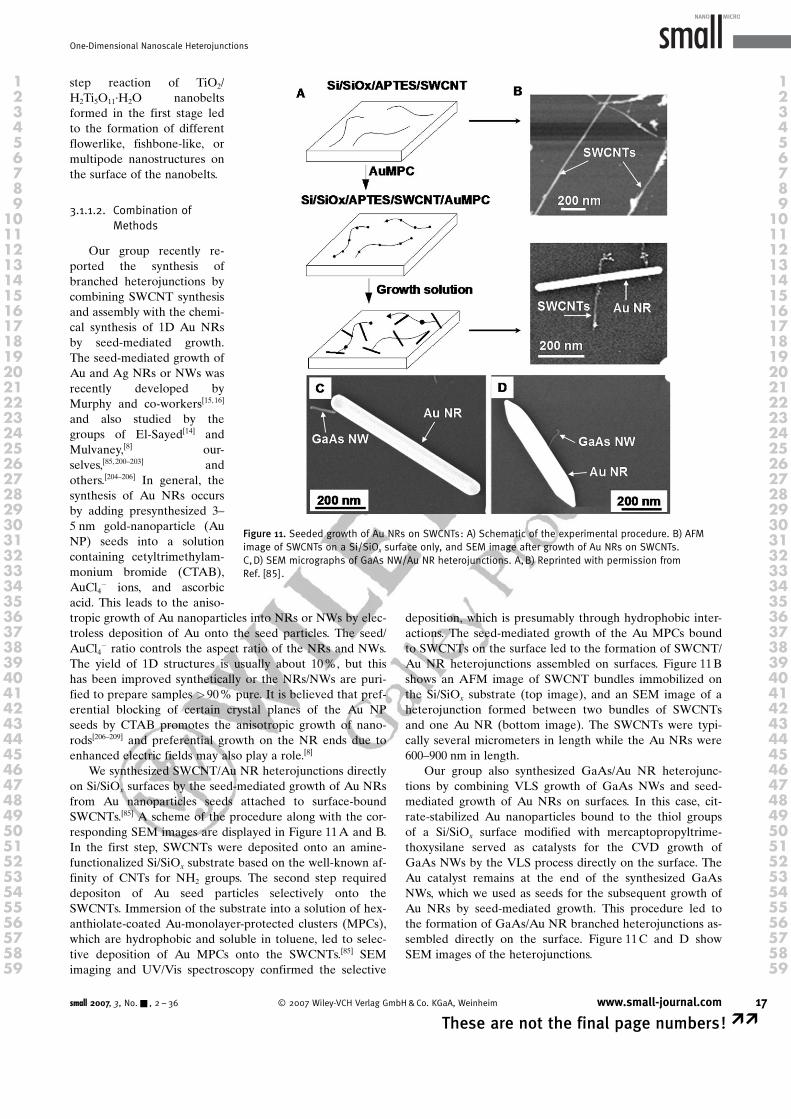
step reaction of TiO2/H2Ti5O11·H2O nanobeltsformed in the first stage ledto the formation of differentflowerlike, fishbone-like, ormultipode nanostructures onthe surface of the nanobelts.
3.1.1.2. Combination ofMethods
Our group recently re-ported the synthesis ofbranched heterojunctions bycombining SWCNT synthesisand assembly with the chemi-cal synthesis of 1D Au NRsby seed-mediated growth.The seed-mediated growth ofAu and Ag NRs or NWs wasrecently developed byMurphy and co-workers[15,16]
and also studied by thegroups of El-Sayed[14] andMulvaney,[8] our-selves,[85, 200–203] andothers.[204–206] In general, thesynthesis of Au NRs occursby adding presynthesized 3–5 nm gold-nanoparticle (AuNP) seeds into a solutioncontaining cetyltrimethylam-monium bromide (CTAB),AuCl4
� ions, and ascorbicacid. This leads to the aniso-tropic growth of Au nanoparticles into NRs or NWs by elec-troless deposition of Au onto the seed particles. The seed/AuCl4
� ratio controls the aspect ratio of the NRs and NWs.The yield of 1D structures is usually about 10%, but thishas been improved synthetically or the NRs/NWs are puri-fied to prepare samples >90% pure. It is believed that pref-erential blocking of certain crystal planes of the Au NPseeds by CTAB promotes the anisotropic growth of nano-rods[206–209] and preferential growth on the NR ends due toenhanced electric fields may also play a role.[8]
We synthesized SWCNT/Au NR heterojunctions directlyon Si/SiOx surfaces by the seed-mediated growth of Au NRsfrom Au nanoparticles seeds attached to surface-boundSWCNTs.[85] A scheme of the procedure along with the cor-responding SEM images are displayed in Figure 11A and B.In the first step, SWCNTs were deposited onto an amine-functionalized Si/SiOx substrate based on the well-known af-finity of CNTs for NH2 groups. The second step requireddepositon of Au seed particles selectively onto theSWCNTs. Immersion of the substrate into a solution of hex-anthiolate-coated Au-monolayer-protected clusters (MPCs),which are hydrophobic and soluble in toluene, led to selec-tive deposition of Au MPCs onto the SWCNTs.[85] SEMimaging and UV/Vis spectroscopy confirmed the selective
deposition, which is presumably through hydrophobic inter-actions. The seed-mediated growth of the Au MPCs boundto SWCNTs on the surface led to the formation of SWCNT/Au NR heterojunctions assembled on surfaces. Figure 11Bshows an AFM image of SWCNT bundles immobilized onthe Si/SiOx substrate (top image), and an SEM image of aheterojunction formed between two bundles of SWCNTsand one Au NR (bottom image). The SWCNTs were typi-cally several micrometers in length while the Au NRs were600–900 nm in length.
Our group also synthesized GaAs/Au NR heterojunc-tions by combining VLS growth of GaAs NWs and seed-mediated growth of Au NRs on surfaces. In this case, cit-rate-stabilized Au nanoparticles bound to the thiol groupsof a Si/SiOx surface modified with mercaptopropyltrime-thoxysilane served as catalysts for the CVD growth ofGaAs NWs by the VLS process directly on the surface. TheAu catalyst remains at the end of the synthesized GaAsNWs, which we used as seeds for the subsequent growth ofAu NRs by seed-mediated growth. This procedure led tothe formation of GaAs/Au NR branched heterojunctions as-sembled directly on the surface. Figure 11C and D showSEM images of the heterojunctions.
Figure 11. Seeded growth of Au NRs on SWCNTs: A) Schematic of the experimental procedure. B) AFMimage of SWCNTs on a Si/SiOx surface only, and SEM image after growth of Au NRs on SWCNTs.C,D) SEM micrographs of GaAs NW/Au NR heterojunctions. A,B) Reprinted with permission fromRef. [85].
small 2007, 3, No.& , 2 – 36 � 2007 Wiley-VCH Verlag GmbH&Co. KGaA, Weinheim www.small-journal.com 17
These are not the final page numbers! ��
One-Dimensional Nanoscale Heterojunctions
1 12 23 34 45 56 67 78 89 9
10 1011 1112 1213 1314 1415 1516 1617 1718 1819 1920 2021 2122 2223 2324 2425 2526 2627 2728 2829 2930 3031 3132 3233 3334 3435 3536 3637 3738 3839 3940 4041 4142 4243 4344 4445 4546 4647 4748 4849 4950 5051 5152 5253 5354 5455 5556 5657 5758 5859 59
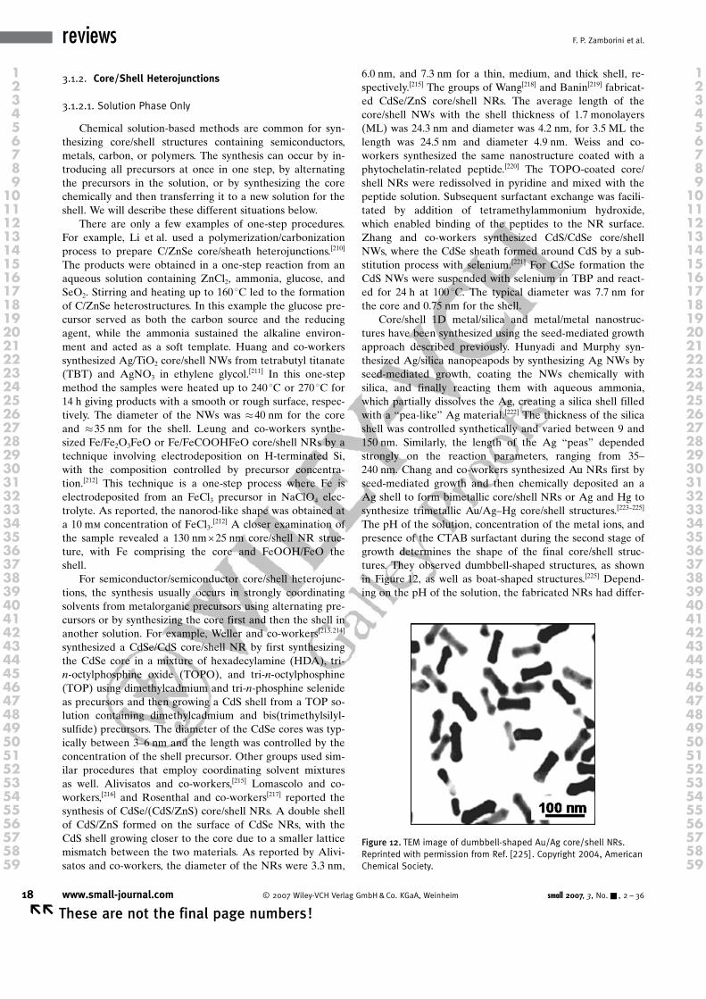
3.1.2. Core/Shell Heterojunctions
3.1.2.1. Solution Phase Only
Chemical solution-based methods are common for syn-thesizing core/shell structures containing semiconductors,metals, carbon, or polymers. The synthesis can occur by in-troducing all precursors at once in one step, by alternatingthe precursors in the solution, or by synthesizing the corechemically and then transferring it to a new solution for theshell. We will describe these different situations below.
There are only a few examples of one-step procedures.For example, Li et al. used a polymerization/carbonizationprocess to prepare C/ZnSe core/sheath heterojunctions.[210]
The products were obtained in a one-step reaction from anaqueous solution containing ZnCl2, ammonia, glucose, andSeO2. Stirring and heating up to 160 8C led to the formationof C/ZnSe heterostructures. In this example the glucose pre-cursor served as both the carbon source and the reducingagent, while the ammonia sustained the alkaline environ-ment and acted as a soft template. Huang and co-workerssynthesized Ag/TiO2 core/shell NWs from tetrabutyl titanate(TBT) and AgNO3 in ethylene glycol.
[211] In this one-stepmethod the samples were heated up to 240 8C or 270 8C for14 h giving products with a smooth or rough surface, respec-tively. The diameter of the NWs was �40 nm for the coreand �35 nm for the shell. Leung and co-workers synthe-sized Fe/Fe2O3FeO or Fe/FeCOOHFeO core/shell NRs by atechnique involving electrodeposition on H-terminated Si,with the composition controlled by precursor concentra-tion.[212] This technique is a one-step process where Fe iselectrodeposited from an FeCl3 precursor in NaClO4 elec-trolyte. As reported, the nanorod-like shape was obtained ata 10 mm concentration of FeCl3.
[212] A closer examination ofthe sample revealed a 130 nmQ25 nm core/shell NR struc-ture, with Fe comprising the core and FeOOH/FeO theshell.
For semiconductor/semiconductor core/shell heterojunc-tions, the synthesis usually occurs in strongly coordinatingsolvents from metalorganic precursors using alternating pre-cursors or by synthesizing the core first and then the shell inanother solution. For example, Weller and co-workers[213,214]
synthesized a CdSe/CdS core/shell NR by first synthesizingthe CdSe core in a mixture of hexadecylamine (HDA), tri-n-octylphosphine oxide (TOPO), and tri-n-octylphosphine(TOP) using dimethylcadmium and tri-n-phosphine selenideas precursors and then growing a CdS shell from a TOP so-lution containing dimethylcadmium and bis(trimethylsilyl-sulfide) precursors. The diameter of the CdSe cores was typ-ically between 3–6 nm and the length was controlled by theconcentration of the shell precursor. Other groups used sim-ilar procedures that employ coordinating solvent mixturesas well. Alivisatos and co-workers,[215] Lomascolo and co-workers,[216] and Rosenthal and co-workers[217] reported thesynthesis of CdSe/ACHTUNGTRENNUNG(CdS/ZnS) core/shell NRs. A double shellof CdS/ZnS formed on the surface of CdSe NRs, with theCdS shell growing closer to the core due to a smaller latticemismatch between the two materials. As reported by Alivi-satos and co-workers, the diameter of the NRs were 3.3 nm,
6.0 nm, and 7.3 nm for a thin, medium, and thick shell, re-spectively.[215] The groups of Wang[218] and Banin[219] fabricat-ed CdSe/ZnS core/shell NRs. The average length of thecore/shell NWs with the shell thickness of 1.7 monolayers(ML) was 24.3 nm and diameter was 4.2 nm, for 3.5 ML thelength was 24.5 nm and diameter 4.9 nm. Weiss and co-workers synthesized the same nanostructure coated with aphytochelatin-related peptide.[220] The TOPO-coated core/shell NRs were redissolved in pyridine and mixed with thepeptide solution. Subsequent surfactant exchange was facili-tated by addition of tetramethylammonium hydroxide,which enabled binding of the peptides to the NR surface.Zhang and co-workers synthesized CdS/CdSe core/shellNWs, where the CdSe sheath formed around CdS by a sub-stitution process with selenium.[221] For CdSe formation theCdS NWs were suspended with selenium in TBP and react-ed for 24 h at 100 8C. The typical diameter was 7.7 nm forthe core and 0.75 nm for the shell.
Core/shell 1D metal/silica and metal/metal nanostruc-tures have been synthesized using the seed-mediated growthapproach described previously. Hunyadi and Murphy syn-thesized Ag/silica nanopeapods by synthesizing Ag NWs byseed-mediated growth, coating the NWs chemically withsilica, and finally reacting them with aqueous ammonia,which partially dissolves the Ag, creating a silica shell filledwith a “pea-like” Ag material.[222] The thickness of the silicashell was controlled synthetically and varied between 9 and150 nm. Similarly, the length of the Ag “peas” dependedstrongly on the reaction parameters, ranging from 35–240 nm. Chang and co-workers synthesized Au NRs first byseed-mediated growth and then chemically deposited an aAg shell to form bimetallic core/shell NRs or Ag and Hg tosynthesize trimetallic Au/Ag–Hg core/shell structures.[223–225]
The pH of the solution, concentration of the metal ions, andpresence of the CTAB surfactant during the second stage ofgrowth determines the shape of the final core/shell struc-tures. They observed dumbbell-shaped structures, as shownin Figure 12, as well as boat-shaped structures.[225] Depend-ing on the pH of the solution, the fabricated NRs had differ-
Figure 12. TEM image of dumbbell-shaped Au/Ag core/shell NRs.Reprinted with permission from Ref. [225]. Copyright 2004, AmericanChemical Society.
18 www.small-journal.com � 2007 Wiley-VCH Verlag GmbH&Co. KGaA, Weinheim small 2007, 3, No.& , 2 – 36
�� These are not the final page numbers!
reviews F. P. Zamborini et al.
1 12 23 34 45 56 67 78 89 9
10 1011 1112 1213 1314 1415 1516 1617 1718 1819 1920 2021 2122 2223 2324 2425 2526 2627 2728 2829 2930 3031 3132 3233 3334 3435 3536 3637 3738 3839 3940 4041 4142 4243 4344 4445 4546 4647 4748 4849 4950 5051 5152 5253 5354 5455 5556 5657 5758 5859 59
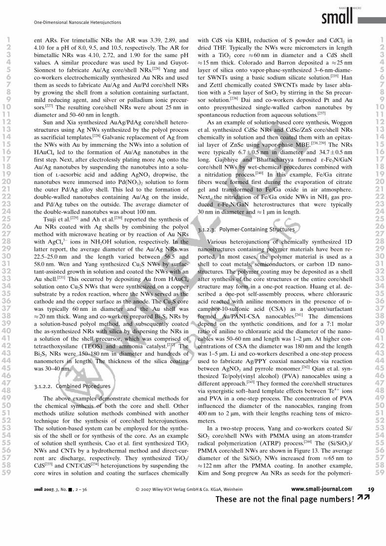
ent ARs. For trimetallic NRs the AR was 3.39, 2.89, and4.10 for a pH of 8.0, 9.5, and 10.5, respectively. The AR forbimetallic NRs was 4.10, 2.72, and 1.90 for the same pHvalues. A similar procedure was used by Liu and Guyot-Sionnest to fabricate Au/Ag core/shell NRs.[226] Yang andco-workers electrochemically synthesized Au NRs and usedthem as seeds to fabricate Au/Ag and Au/Pd core/shell NRsby growing the shell from a solution containing surfactant,mild reducing agent, and silver or palladium ionic precur-sors.[227] The resulting core/shell NRs were about 25 nm indiameter and 50–60 nm in length.
Sun and Xia synthesized AuAg/PdAg core/shell hetero-structures using Ag NWs synthesized by the polyol processas sacrificial templates.[228] Galvanic replacement of Ag fromthe NWs with Au by immersing the NWs into a solution ofHAuCl4 led to the formation of Au/Ag nanotubes in thefirst step. Next, after electrolessly plating more Ag onto theAu/Ag nanotubes by suspending the nanotubes into a solu-tion of l-acsorbic acid and adding AgNO3 dropwise, thenanotubes were immersed into PdACHTUNGTRENNUNG(NO3)2 solution to formthe outer Pd/Ag alloy shell. This led to the formation ofdouble-walled nanotubes containing Au/Ag on the inside,and Pd/Ag tubes on the outside. The average diameter ofthe double-walled nanotubes was about 100 nm.
Tsuji et al.[229] and Ah et al.[230] reported the synthesis ofAu NRs coated with Ag shells by combining the polyolmethod with microwave heating or by reaction of Au NRswith AgCl4
3� ions in NH2OH solution, respectively. In thelatter report, the average diameter of the Au/Ag NRs was22.5–25.0 nm and the length varied between 56.5 and58.0 nm. Wen and Yang synthesized Cu2S NWs by surfac-tant-assisted growth in solution and coated the NWs with anAu shell.[231] This occurred by depositing Au from HAuCl4solution onto Cu2S NWs that were synthesized on a coppersubstrate by a redox reaction, where the NWs served as thecathode and the copper surface as the anode. The Cu2S corewas typically 60 nm in diameter and the Au shell was�20 nm thick. Wang and co-workers prepared Bi2S3 NRs bya solution-based polyol method, and subsequently coatedthe as-synthesized NRs with silica by dispersing the NRs ina solution of the shell precursor, which was comprised oftetraethoxysilane (TEOS) and ammonia catalyst.[232] TheBi2S3 NRs were 150–180 nm in diameter and hundreds ofnanometers in length. The thickness of the silica coatingwas 30–40 nm.
3.1.2.2. Combined Procedures
The above examples demonstrate chemical methods forthe chemical synthesis of both the core and shell. Othermethods utilize solution methods combined with anothertechnique for the synthesis of core/shell heterojunctions.The solution-based system can be employed for the synthe-sis of the shell or for synthesis of the core. As an exampleof solution shell synthesis, Cao et al. first synthesized TiO2
NWs and CNTs by a hydrothermal method and direct-cur-rent arc discharge, respectively. They synthesized TiO2/CdS[233] and CNT/CdS[234] heterojunctions by suspending thecore wires in solution and coating the surfaces chemically
with CdS via KBH4 reduction of S powder and CdCl2 indried THF. Typically the NWs were micrometers in lengthwith a TiO2 core �60 nm in diameter and a CdS shell�15 nm thick. Colorado and Barron deposited a �25 nmlayer of silica onto vapor-phase-synthesized 3–6-nm-diame-ter SWNTs using a basic sodium silicate solution.[235] Hanand Zettl chemically coated SWCNTs made by laser abla-tion with a 5-nm layer of SnO2 by stirring in the Sn precur-sor solution.[236] Dai and co-workers deposited Pt and Auonto presynthesized single-walled carbon nanotubes byspontaneous reduction from aqueous solutions.[237]
As an example of solution-based core synthesis, Woggonet al. synthesized CdSe NRs and CdSe/ZnS core/shell NRschemically in solution and then coated them with an epitax-ial layer of ZnSe using vapor-phase MBE.[238,239] The NRswere typically 6.7�0.5 nm in diameter and 34.7�0.5 nmlong. Gajbhiye and Bhattacharyya formed e-Fe3N/GaNcore/shell NWs by wet-chemical procedures combined witha nitridation process.[240] In this example, Fe/Ga citratefibers were formed first during the evaporation of citrategel and transformed to Fe/Ga oxide in air atmosphere.Next, the nitridation of Fe/Ga oxide NWs in NH3 gas pro-duced e-Fe3N/GaN heterostructures that were typically30 nm in diameter and �1 mm in length.
3.1.2.3. Polymer-Containing Structures
Various heterojunctions of chemically synthesized 1Dnanostructures containing polymer materials have been re-ported. In most cases, the polymer material is used as ashell to coat metals, semiconductors, or carbon 1D nano-structures. The polymer coating may be deposited as a shellafter synthesis of the core structures or the entire core/shellstructure may form in a one-pot reaction. Huang et al. de-scribed a one-pot self-assembly process, where chlorauricacid reacted with aniline monomers in the presence of d-camphor-10-sulfonic acid (CSA) as a dopant/surfactantformed Au/PANI-CSA nanocables.[241] The dimensionsdepend on the synthetic conditions, and for a 7:1 molarratio of aniline to chlorauric acid the diameter of the nano-cables was 50–60 nm and length was 1–2 mm. At higher con-centrations of CSA the diameter was 180 nm and the lengthwas 1–5 mm. Li and co-workers described a one-step processused to fabricate Ag/PPY coaxial nanocables via reactionbetween AgNO3 and pyrrole monomer.
[242] Qian et al. syn-thesized Te/poly(vinyl alcohol) (PVA) nanocables using adifferent approach.[243] They formed the core/shell structuresvia synergistic soft–hard template effects between Te4+ ionsand PVA in a one-step process. The concentration of PVAinfluenced the diameter of the nanocables, ranging from400 nm to 2 mm, with their lengths reaching tens of micro-meters.
In a two-step process, Yang and co-workers coated Si/SiO2 core/shell NWs with PMMA using an atom-transferradical polymerization (ATRP) process.[244] The (Si/SiO2)/PMMA core/shell NWs are shown in Figure 13. The averagediameter of the Si/SiO2 NWs increased from �65 nm to�122 nm after the PMMA coating. In another example,Kim and Song pregrew Au NRs as seeds for the polymeri-
small 2007, 3, No.& , 2 – 36 � 2007 Wiley-VCH Verlag GmbH&Co. KGaA, Weinheim www.small-journal.com 19
These are not the final page numbers! ��
One-Dimensional Nanoscale Heterojunctions
1 12 23 34 45 56 67 78 89 9
10 1011 1112 1213 1314 1415 1516 1617 1718 1819 1920 2021 2122 2223 2324 2425 2526 2627 2728 2829 2930 3031 3132 3233 3334 3435 3536 3637 3738 3839 3940 4041 4142 4243 4344 4445 4546 4647 4748 4849 4950 5051 5152 5253 5354 5455 5556 5657 5758 5859 59
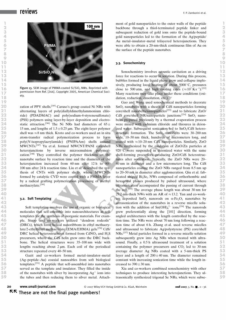
zation of PPY shells.[245] CarusoGs group coated Ni NRs withalternating layers of poly(diallyldimethylammonium chlo-ride) (PDADMAC) and poly(sodium-4-styrenesulfonate)(PSS) polymers using layer-by-layer deposition and electro-static attraction.[246] The Ni NRs had diameters of 65�15 nm, and lengths of 1.5�0.25 mm. The eight-layer polymershell was �8 nm thick. Kroto and co-workers used an in situatom-transfer radical polymerization process to formpoly(N-isopropylacrylamide) (PNIPAAm) shells aroundMWCNTs.[247] Yu et al. formed MWCNT/PANI core/shellheterojunctions by inverse microemulsion polymeri-zation.[248] They controlled the polymer thickness on thenanotube surface by reaction time and the diameter of theheterojunction increased from 60 nm after 12 h to 80–100 nm after 24 h reaction time. Liu et al. described the syn-thesis of CNTs with polymer shells, where MWCNTsformed by catalytic CVD were coated with a PMMA layerby a radical grafting polymerization processing of methylmethacrylate.[249]
3.2. Soft Templating
Soft templating involves the use of organic or biologicalmolecules that self-assemble into nanoarchitectures as softtemplates for the synthesis of inorganic materials. For exam-ple, Stupp and co-workers utilized “dendron rodcoils”(DRCs), which form helical nanoribbons in ethyl methacry-late/2-ethylhexyl methacrylate (EMA/EHMA) gels.[250] CdS/DRC helical heterostructures formed from CdNO3 and H2Sprecursors, where the CdS helix grew onto the DRC back-bone. The helical structures were 35–100 nm wide withlengths reaching about 2 mm. Each coil of the periodicalstructure repeated every 40–50 nm.
Gazit and co-workers formed metal–insulator–metal(Ag–peptide–Au) coaxial nanocables from soft biologicaltemplates.[251] A peptide that self-assembled into nanotubesserved as the template and insulator. They filled the insideof the nanotubes with silver by incorporating Ag+ ions intothe tubes and then reducing them to silver metal. Attach-
ment of gold nanoparticles to the outer walls of the peptidebackbone through a thiol-terminated peptide linker andsubsequent reduction of gold ions onto the peptide-boundgold nanoparticles led to the formation of the Ag/peptide/Au metal–insulator–metal trilayered heterojunctions. Theywere able to obtain a 20-nm-thick continuous film of Au onthe surface of the peptide nanotubes.
3.3. Sonochemistry
Sonochemistry involves acoustic cavitation as a drivingforce for reactions to occur in solution. During this process,bubbles formed in the liquid phase grow and collapse implo-sively, producing local heating of about 5000 8C, pressuresclose to 500 atm, and high cooling rates (�107 Ks�1).[252]Many reactions may take place under these conditions (oxi-dation, reduction, dissolution, etc.).
Gao and Wang used sonochemical methods to decorateSnO2 nanobelts with a sheath of CdS nanoparticles formingcore/shell nanobelts/nanoparticles[253] and to fabricate ZnO/CdS core/shell NR/nanoparticle junctions.[254] SnO2 nano-belts prepared previously by a thermal evaporation processwere mixed with cadmium chloride and thiourea in deion-ized water. Subsequent sonication led to SnO2/CdS hetero-structure formation. The SnO2 nanobelts were 30–200 nmwide, 10–50 nm thick, hundreds of micrometers long, andcoated with �10–20 nm CdS nanoparticles. Similarly, ZnONRs synthesized by the oxidation of ZnO/Zn particles at920 8C were suspended in deionized water with the sameshell-forming precursors, producing ZnO/CdS heterostruc-tures after sonication. Typically, the ZnO NRs were 20–40 nm in diameter and a few micrometers long. The CdSnanoparticles coating the ZnO NRs ranged from 8.5 nm upto 20–50 nm in diameter after agglomeration. Qiu et al. fab-ricated striped Bi2Se3 NWs composed of orthorhombic andhexagonal phases produced by pulsed ultrasound, whereultrasonication accompanied the passing of current throughthe cell.[255] The average phase length was about 30 nm for29.2-nm-thick NWs with an AR of �13.2. Yan and co-work-ers deposited SnO2 nanorods on a-Fe2O3 nanotubes byultrasonication of the nanotubes in a reverse micelle solu-tion with the addition of Sn(OH)6
2� ions.[256] The nanorodsgrew preferentially along the [101] direction, formingangled architectures with the length controlled by the reac-tion time. The NRs were about 70 nm long following a reac-tion time of about 6 h. Zhang et al. used reverse micellesand ultrasound to fabricate Ag/polystyrene (PS) core/shellNRs.[257] Metal particles formed in a reverse micelle solutionsubsequently grew into Ag NRs when treated with ultra-sound. Finally, a 0.5 h ultrasound treatment of a solutioncontaining the polymer precursors and CO2 led to 30 nmaverage diameter Ag NRs coated with a 5-nm-thick PSlayer and a length of 200�40 nm. The diameter remainedconstant with increasing sonication time while the length in-creased to 390�30 nm.
Xia and co-workers combined sonochemistry with othertechniques to produce interesting heterojunctions. They ul-trasonically synthesized trigonal Se NRs, which were subse-
Figure 13. SEM image of PMMA-coated Si/SiO2 NWs. Reprinted withpermission from Ref. [244]. Copyright 2005, American Chemical Soci-ety.
20 www.small-journal.com � 2007 Wiley-VCH Verlag GmbH&Co. KGaA, Weinheim small 2007, 3, No.& , 2 – 36
�� These are not the final page numbers!
reviews F. P. Zamborini et al.
1 12 23 34 45 56 67 78 89 9
10 1011 1112 1213 1314 1415 1516 1617 1718 1819 1920 2021 2122 2223 2324 2425 2526 2627 2728 2829 2930 3031 3132 3233 3334 3435 3536 3637 3738 3839 3940 4041 4142 4243 4344 4445 4546 4647 4748 4849 4950 5051 5152 5253 5354 5455 5556 5657 5758 5859 59
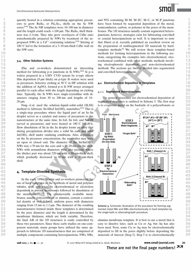
quently heated in a solution containing appropriate precur-sors to grow RuSe2 or Pd17Se15 shells on the Se NWcores.[258] The Se NR templates were 10–100 nm in diameterand the length could reach �100 mm. The RuSe2 shell thick-ness was 2–4 nm. They also grew overlayers of CdSe ontosonochemically prepared Se NWs by treatment of the as-prepared NWs in a Cd2+-containing solution.[259] Stirring at100 8C led to the formation of a 5–10-nm-thick CdSe wall onthe NW core.
3.4. Other Solution Systems
Zhu and co-workers demonstrated an interestingmethod for fabricating p–n junctions in Si NWs.[260] Si p–nwafers prepared in a UHV CVD system by n-type siliconfilm deposition (9 mm thick) on p-type Si wafers were usedas precursors. Selective etching at 50 8C in HF solution withthe addition of AgNO3 formed p–n Si NW arrays arrangedparallel to each other with the length depending on etchingtime. Typically, the Si NWs were single-crystalline with di-ameters ranging from 30 to 200 nm and lengths of 10–20 mm.
Fang et al. used the solution–liquid–solid–solid (SLSS)method to fabricate Sn-filled In(OH)3 nanotubes.
[261] This isa single-step procedure where the liquid part of an In–Sndroplet serves as a catalyst and source of precursors to thenanostructure at the same time. In foil, Sn foil, and NaOHserved as precursors, and were heated at 180 8C for 30 h.Slow dissolution of Sn in the In droplet forms an alloy thatduring precipitation divides into a solid Sn core and solidIn(OH)3 shell under oxidizing conditions. Also, dependingon the In precursor concentration, the nanotubes may havean open or closed end. The diameter of the Sn/In(OH)3NWs was �70 nm for the core and �10–20 nm for the shell.NWs with nonuniform diameters were also present, wherethe thicker part was about 220 nm with a 50-nm-thick shell,which gradually decreased to 80 nm with a 20-nm-thickshell.
4. Template-Directed Synthesis
In the early 1990s, Martin and co-workers pioneered theuse of hard templates in the synthesis of metal and polymertubules, rods, and wires by electrochemical or electrolessdeposition in porous membranes followed by dissolution ofthe membrane.[262, 263] The commercially available mem-branes, usually polycarbonate or alumina, contain a control-led density of well-defined, uniform pores with diametersranging from 15 nm to 1.2 mm. The diameter of the resultingnanostructures formed inside these templates is determinedby the pore diameter and the length is determined by themembrane thickness, which are both variable. Therefore,the final AR of the 1D structures is easily controlled bythese two parameters. Since these early studies on one-com-ponent materials, many groups have utilized the same ap-proach to fabricate 1D nanostructures that are comprised ofmultiple components containing heterojunctions. NWs, NRs,
and NTs containing M–M, M–SC, M–C, or M–P junctionshave been formed by sequential deposition of the metal,semiconductor, carbon, or polymer in the pores of the mem-branes. The 1D structures usually contain segmented hetero-junctions, however, strategies exist for fabricating core/shellor coaxial heterojunctions as well. It is important to notethat Hurst et al. recently published an excellent review onthe preparation of multisegmented 1D nanorods by hard-template methods.[4] We will review these template-basedmethods for forming heterojunctions in the following sec-tions, categorizing the examples into electrochemical, elec-trochemical combined with other methods, methods involv-ing electrophoretic deposition, and non-electrochemicalmethods. The sections are further divided into segementedand core/shell heterojunctions.
4.1. Electrochemical Deposition in Templates
4.1.1. Segmented Heterojunctions
The general procedure for electrochemical deposition ofsegmented structures is outlined in Scheme 3. The first stepis to evaporate metal on the backside of a polycarbonate or
alumina membrane template. It is best to use a metal that iseasy to dissolve later, such as Cu or Ag, but Au has alsobeen used. Next, some Cu or Ag may be electrochemicallydeposited to fill in the pores slightly before depositing thematerials of interest (Step 2). Step 3 is to electrochemically
Scheme 3. Schematic illustration of the procedure for forming seg-mented metal NRs and NWs electrochemically in hard templates bythe single-bath or alternating-bath procedure.
small 2007, 3, No.& , 2 – 36 � 2007 Wiley-VCH Verlag GmbH&Co. KGaA, Weinheim www.small-journal.com 21
These are not the final page numbers! ��
One-Dimensional Nanoscale Heterojunctions
1 12 23 34 45 56 67 78 89 9
10 1011 1112 1213 1314 1415 1516 1617 1718 1819 1920 2021 2122 2223 2324 2425 2526 2627 2728 2829 2930 3031 3132 3233 3334 3435 3536 3637 3738 3839 3940 4041 4142 4243 4344 4445 4546 4647 4748 4849 4950 5051 5152 5253 5354 5455 5556 5657 5758 5859 59
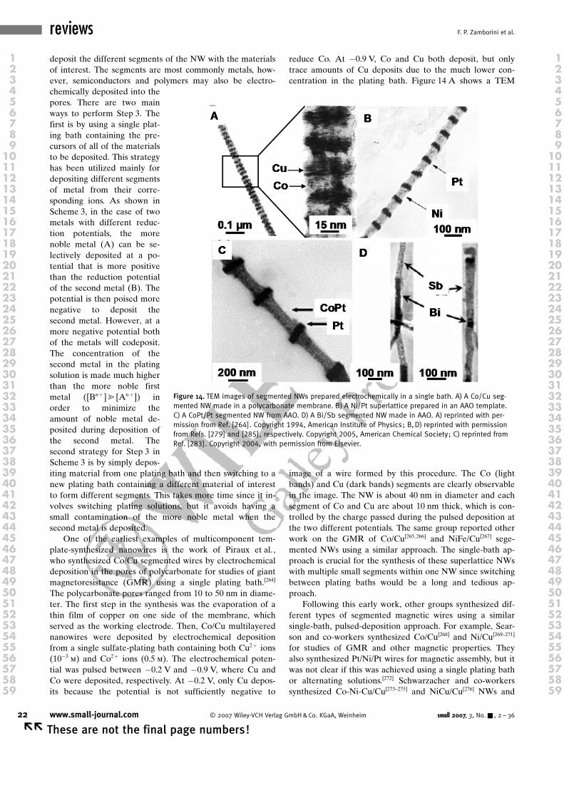
deposit the different segments of the NW with the materialsof interest. The segments are most commonly metals, how-ever, semiconductors and polymers may also be electro-chemically deposited into thepores. There are two mainways to perform Step 3. Thefirst is by using a single plat-ing bath containing the pre-cursors of all of the materialsto be deposited. This strategyhas been utilized mainly fordepositing different segmentsof metal from their corre-sponding ions. As shown inScheme 3, in the case of twometals with different reduc-tion potentials, the morenoble metal (A) can be se-lectively deposited at a po-tential that is more positivethan the reduction potentialof the second metal (B). Thepotential is then poised morenegative to deposit thesecond metal. However, at amore negative potential bothof the metals will codeposit.The concentration of thesecond metal in the platingsolution is made much higherthan the more noble firstmetal ([Bn+]@ [An+]) inorder to minimize theamount of noble metal de-posited during deposition ofthe second metal. Thesecond strategy for Step 3 inScheme 3 is by simply depos-iting material from one plating bath and then switching to anew plating bath containing a different material of interestto form different segments. This takes more time since it in-volves switching plating solutions, but it avoids having asmall contamination of the more noble metal when thesecond metal is deposited.
One of the earliest examples of multicomponent tem-plate-synthesized nanowires is the work of Piraux et al. ,who synthesized Co/Cu segmented wires by electrochemicaldeposition in the pores of polycarbonate for studies of giantmagnetoresistance (GMR) using a single plating bath.[264]
The polycarbonate pores ranged from 10 to 50 nm in diame-ter. The first step in the synthesis was the evaporation of athin film of copper on one side of the membrane, whichserved as the working electrode. Then, Co/Cu multilayerednanowires were deposited by electrochemical depositionfrom a single sulfate-plating bath containing both Cu2+ ions(10�3 m) and Co2+ ions (0.5 m). The electrochemical poten-tial was pulsed between �0.2 V and �0.9 V, where Cu andCo were deposited, respectively. At �0.2 V, only Cu depos-its because the potential is not sufficiently negative to
reduce Co. At �0.9 V, Co and Cu both deposit, but onlytrace amounts of Cu deposits due to the much lower con-centration in the plating bath. Figure 14 A shows a TEM
image of a wire formed by this procedure. The Co (lightbands) and Cu (dark bands) segments are clearly observablein the image. The NW is about 40 nm in diameter and eachsegment of Co and Cu are about 10 nm thick, which is con-trolled by the charge passed during the pulsed deposition atthe two different potentials. The same group reported otherwork on the GMR of Co/Cu[265,266] and NiFe/Cu[267] sege-mented NWs using a similar approach. The single-bath ap-proach is crucial for the synthesis of these superlattice NWswith multiple small segments within one NW since switchingbetween plating baths would be a long and tedious ap-proach.
Following this early work, other groups synthesized dif-ferent types of segmented magnetic wires using a similarsingle-bath, pulsed-deposition approach. For example, Sear-son and co-workers synthesized Co/Cu[268] and Ni/Cu[269–271]
for studies of GMR and other magnetic properties. Theyalso synthesized Pt/Ni/Pt wires for magnetic assembly, but itwas not clear if this was achieved using a single plating bathor alternating solutions.[272] Schwarzacher and co-workerssynthesized Co-Ni-Cu/Cu[273–275] and NiCu/Cu[276] NWs and
Figure 14. TEM images of segmented NWs prepared electrochemically in a single bath. A) A Co/Cu seg-mented NW made in a polycarbonate membrane. B) A Ni/Pt superlattice prepared in an AAO template.C) A CoPt/Pt segmented NW from AAO. D) A Bi/Sb segmented NW made in AAO. A) reprinted with per-mission from Ref. [264]. Copyright 1994, American Institute of Physics; B,D) reprinted with permissionfrom Refs. [279] and [285], respectively. Copyright 2005, American Chemical Society; C) reprinted fromRef. [283]. Copyright 2004, with permission from Elsevier.
22 www.small-journal.com � 2007 Wiley-VCH Verlag GmbH&Co. KGaA, Weinheim small 2007, 3, No.& , 2 – 36
�� These are not the final page numbers!
reviews F. P. Zamborini et al.
1 12 23 34 45 56 67 78 89 9
10 1011 1112 1213 1314 1415 1516 1617 1718 1819 1920 2021 2122 2223 2324 2425 2526 2627 2728 2829 2930 3031 3132 3233 3334 3435 3536 3637 3738 3839 3940 4041 4142 4243 4344 4445 4546 4647 4748 4849 4950 5051 5152 5253 5354 5455 5556 5657 5758 5859 59

studied GMR and remanant magnetization of the nano-structures. Bai and co-workers fabricated Ni/Cu particles[277]
from Ni/Cu segmented nanowires and prepared arrays ofNi/Cu[278] and Ni/Pt[279] segmented wires with enhanced coer-civity and high remanence ratio. A TEM image of a 50-nm-diameter Ni/Pt nanowire is shown in Figure 14B. Other ex-amples of single-plating-bath approaches include the fabri-cation of Ni/Cu,[280] Au/Co,[281] Co/Cu,[282] CoPt/Pt,[283] andNi/CuSn/Ni[284] segmentedNWs for studies of magneticproperties, spin valves, andmagnetic manipulation. Fig-ure 14C shows an exampleof a bamboo-shaped CoPt/Ptnanowire resulting from thin-ner 300-nm-long segments ofCoPt compared to the thick-er 20-nm-long Pt segments,which is thought to occur bypartial etching of Co in theacidic electrolyte solution.[283]
Finally, Xue et al. synthe-sized segmented Bi/Sb super-lattice nanowires by electro-deposition in anodic aluminatemplates from a single etha-nol plating bath.[285] Fig-ure 14D shows a TEM imageof two of the four differentkinds of structures synthe-sized.[285] Blondel et al. pre-pared Co/Cu segmentedNWs by single-bath and al-ternating-bath techniquesand compared the magneto-resistance of the preparedstructures.[286]
Several groups have alsoused alternating plating solu-tions (Scheme 3) to synthe-size NWs with various elec-trochemically deposited metal, semiconducting, or polymersegments. One of the early examples is the work of Natan,Mallouk, and co-workers, who synthesized striped Au/Ptnanorods inside an alumina template by evaporating Ag onthe backside of the membrane, electrochemically depositinga small amount of Ag inside the pores, and finally electro-chemically depositing segments of Au and Pt sequentiallyfrom separate commercially available plating solutions.[287]
The Ag and alumina membrane were then dissolved to re-lease the striped Au/Pt nanorods, which were suspended insolution. The different chemistry of Au and Pt allowed forselective assembly of different molecules on the two seg-ments. Following this work, Natan and co-workers synthe-sized various striped nanorods in alumina templates, whichthey refer to as metallic barcodes.[42,288–291] Au/Ag rods arethe most common, but they have also demonstrated rodscontaining Pd, Pt, Ni, Cu, and Co by sequential depositionin alumina templates using alternating plating baths of the
individual metal. The rod diameters are generally 200–300 nm with lengths of 4–10 mm. The different metal seg-ments are distinguishable optically by their different reflec-tivity. Changing the lengths of the segments and the metalleads to a variety of different patterns (barcodes). The met-allic barcodes can be used to detect biological moleculesbased on bioassay chemistry and optical detection.[42] Fig-ure 15 A and B shows the optical image and SEM image of
a striped Au/Ag nanorod, respectively.[288] The segments areobservable in both images. The five Au segments are con-stant at 550 nm in length and the variable Ag segments are60, 110, 170, and 240 nm in length from bottom to top.[288]
The Ag segments appear brighter in the optical image dueto its higher reflectivity. Note that in these examples of al-ternating plating baths, there are generally fewer and longersegments compared to the single-bath NWs, partially due tothe inconvenience of switching baths and the fact that super-lattices were not required for this application. Keating andco-workers also synthesized Au/Ag metal barcodes andthose containing other metals such as Co, Cu, Ni, Pt, andPd.[292–294] These studies were aimed at understanding theirreflectivity,[292] fluorescence,[292] stability,[293] and issues relat-ed to DNA-hybridization efficiency.[294]
Mallouk and co-workers synthesized Au/CdSe/Au andNi/CdSe/Ni segmented NWs by alternating the electrochem-ical deposition in polycarbonate membranes using commer-
Figure 15. A) Optical image of an Au–Ag striped nanorod with corresponding FE-SEM image of the sameheterostructure in (B). C) SEM image of Au/CdSe/Au nanowires synthesized in a polycarbonate mem-brane. D) SEM image of a Au/Ni nanowire bundle with ferromagnetic attraction. A,B) are from Ref. [288],reprinted with permission from AAAS. C) Reprinted with permission from Ref. [295]. Copyright 2002,American Chemical Society. D) Reprinted with permission from Ref. [300]. Copyright 2003, AmericanChemical Society.
small 2007, 3, No.& , 2 – 36 � 2007 Wiley-VCH Verlag GmbH&Co. KGaA, Weinheim www.small-journal.com 23
These are not the final page numbers! ��
One-Dimensional Nanoscale Heterojunctions
1 12 23 34 45 56 67 78 89 9
10 1011 1112 1213 1314 1415 1516 1617 1718 1819 1920 2021 2122 2223 2324 2425 2526 2627 2728 2829 2930 3031 3132 3233 3334 3435 3536 3637 3738 3839 3940 4041 4142 4243 4344 4445 4546 4647 4748 4849 4950 5051 5152 5253 5354 5455 5556 5657 5758 5859 59
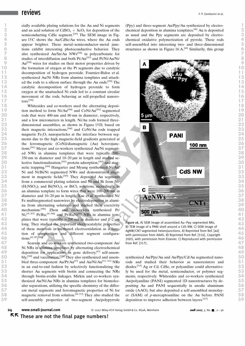
cially available plating solutions for the Au and Ni segmentsand an acid solution of CdSO4 + SeO2 for deposition of thesemiconducting CdSe segment.[295] The SEM image in Fig-ure 15C shows the Au/CdSe/Au wires, where the Au endsappear brighter. These metal–semiconductor–metal junc-tions exhibit interesting photoconductive behavior. Theyalso synthesized Au/Sn/Au NWs[296] in polycarbonate forstudies of interdiffusion and both Pt/Au[297] and Pt/Ni/Au/Ni/Au[298] wires for studies on their motor properties driven bythe formation of oxygen at the Pt segments due to catalyticdecomposition of hydrogen peroxide. Fournier-Bidoz et al.synthesized Au/Ni NRs from alumina templates and attach-ed the rods to a silicon surface through the Au ends.[299] Thecatalytic decomposition of hydrogen peroxide to formoxygen at the unattached Ni ends led to a constant circularmovement of the rods, behaving as self-propelled nanoro-tors.[299]
Whitesides and co-workers used the alternating deposi-tion method to form Ni/Au[300] and CoNi/Au[301] segmentedrods that were 400 nm and 80 nm in diameter, respectively,and a few micrometers in length. Ni/Au rods formed three-dimensional assemblies, as shown in Figure 15D, based ontheir magnetic interactions,[300] and CoNi/Au rods trappedmagnetic Fe2O3 nanoparticles at the interface between seg-ments due to the high magnetic-field gradients generated atthe ferromagnetic (CoNi)/diamagnetic (Au) heterojunc-tions.[301] Meyer and co-workers synthesized Au/Ni segment-ed NWs in alumina templates that were typically 200–350 nm in diameter and 10–20 mm in length and studied se-lective functionalization,[302] protein adsorption,[303] and mag-netic trapping.[304] Hangarter and Myung synthesized Ni/Au/Ni and Ni/Bi/Ni segmented NWs and demonstrated align-ment in magnetic fields.[305] They deposited Au segmentsfrom a commercial plating solution and Ni and Bi from Ni-ACHTUNGTRENNUNG(H2NSO3)2 and BiACHTUNGTRENNUNG(NO3)3 or BiCl2 solutions, accordingly, inan alumina template to form wires that were 100–200 nm indiameter and 10–20 mm in length. Xue et al. synthesized Ni/Fe multisegmented nanowires by electrodeposition in alumi-na from alternating solutions and studied their coercivitymechanism.[306] Zhou and co-workers synthesized Pt/Ni,[45, 307] Pt/Ru,[45, 308] and Pt/RuNi[45] NRs in alumina tem-plates that were typically �200 nm in diameter and 1–2 mmlong. They studied the important electrocatalytic propertiesof these materials in methanol electrooxidation as a func-tion of composition and different segment configura-tions.[45, 307,308]
Searson and co-workers synthesized two-component Au/Ni NRs in alumina templates by alternating electrochemicaldeposition for applications in gene delivery,[43] self-assem-bly,[309] and vaccination.[310] They also synthesized and assem-bled three-component Au/Pt/Au[47] and Au/Ni/Au[311,312] NRsin an end-to-end fashion by selectively functionalizing theshorter Au segments with biotin and connecting the NRsthrough biotin-avidin linkages. Mirkin and co-workers syn-thesized Au/Ni/Au NRs in alumina templates for biomolec-ular separations, utilizing the specific chemistry of the differ-ent metal segments and ferromagnetic properties of Ni formagnetic removal from solution.[44, 313] They also studied theself-assembly properties of two-segment Au/polypyrrole
(Ppy) and three-segment Au/Ppy/Au synthesized by electro-chemical deposition in alumina templates.[46] Au is depositedas usual and the Ppy segments are deposited by electro-chemical oxidative polymerization of pyrrole. These rodsself-assembled into interesting two- and three-dimensionalstructures as shown in Figure 16 A.[46] Similarily, this group
synthesized Au/Ppy/Au and Au/Ppy/Cd/Au segmented nano-rods and studied their behavior as nanoresistors anddiodes.[314] Ag or Cd, CdSe, or polyaniline could alternative-ly be used for the metal, semiconductor, or polymer seg-ments, respectively. Whitesides and co-workers synthesizedAu/polyaniline (PANI) segmented 1D nanostructures by de-positing Au and PANI sequentially in anodic aluminumoxide (AAO), but also deposited a self-assembled monolay-er (SAM) of p-mercaptoaniline on the Au before PANIdeposition to improve adhesion between layers.[315]
Figure 16. A) SEM image of assembled Au–Ppy segmented NRs.B) TEM image of a PANI shell around a CdS NW. C) SEM image ofAgNW/CNT segmented heterojunctions. A) Reprinted from Ref. [46]with permission from AAAS. B) Reprinted from Ref. [316]. Copyright2005, with permission from Elsevier. C) Reproduced with permissionfrom Ref. [317].
24 www.small-journal.com � 2007 Wiley-VCH Verlag GmbH&Co. KGaA, Weinheim small 2007, 3, No.& , 2 – 36
�� These are not the final page numbers!
reviews F. P. Zamborini et al.
1 12 23 34 45 56 67 78 89 9
10 1011 1112 1213 1314 1415 1516 1617 1718 1819 1920 2021 2122 2223 2324 2425 2526 2627 2728 2829 2930 3031 3132 3233 3334 3435 3536 3637 3738 3839 3940 4041 4142 4243 4344 4445 4546 4647 4748 4849 4950 5051 5152 5253 5354 5455 5556 5657 5758 5859 59
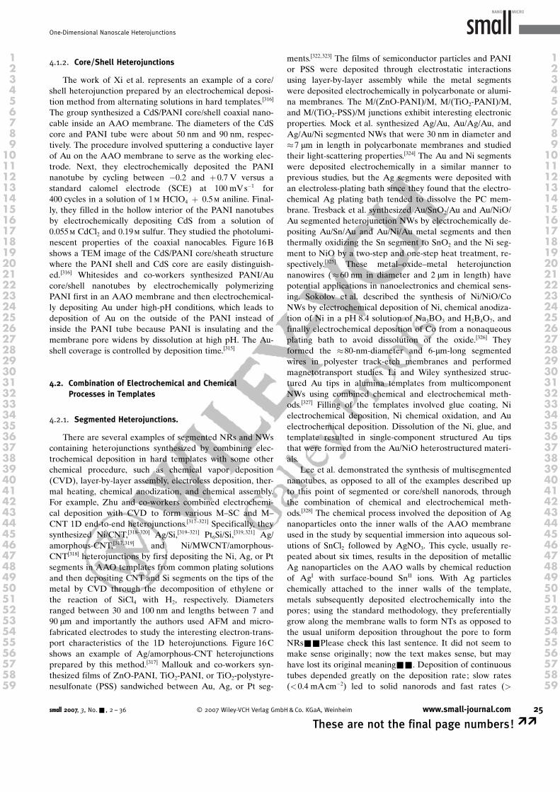
4.1.2. Core/Shell Heterojunctions
The work of Xi et al. represents an example of a core/shell heterojunction prepared by an electrochemical deposi-tion method from alternating solutions in hard templates.[316]
The group synthesized a CdS/PANI core/shell coaxial nano-cable inside an AAO membrane. The diameters of the CdScore and PANI tube were about 50 nm and 90 nm, respec-tively. The procedure involved sputtering a conductive layerof Au on the AAO membrane to serve as the working elec-trode. Next, they electrochemically deposited the PANInanotube by cycling between �0.2 and +0.7 V versus astandard calomel electrode (SCE) at 100 mVs�1 for400 cycles in a solution of 1m HClO4 + 0.5m aniline. Final-ly, they filled in the hollow interior of the PANI nanotubesby electrochemically depositing CdS from a solution of0.055m CdCl2 and 0.19m sulfur. They studied the photolumi-nescent properties of the coaxial nanocables. Figure 16Bshows a TEM image of the CdS/PANI core/sheath structurewhere the PANI shell and CdS core are easily distinguish-ed.[316] Whitesides and co-workers synthesized PANI/Aucore/shell nanotubes by electrochemically polymerizingPANI first in an AAO membrane and then electrochemical-ly depositing Au under high-pH conditions, which leads todeposition of Au on the outside of the PANI instead ofinside the PANI tube because PANI is insulating and themembrane pore widens by dissolution at high pH. The Au-shell coverage is controlled by deposition time.[315]
4.2. Combination of Electrochemical and ChemicalProcesses in Templates
4.2.1. Segmented Heterojunctions.
There are several examples of segmented NRs and NWscontaining heterojunctions synthesized by combining elec-trochemical deposition in hard templates with some otherchemical procedure, such as chemical vapor deposition(CVD), layer-by-layer assembly, electroless deposition, ther-mal heating, chemical anodization, and chemical assembly.For example, Zhu and co-workers combined electrochemi-cal deposition with CVD to form various M–SC and M–CNT 1D end-to-end heterojunctions.[317–321] Specifically, theysynthesized Ni/CNT,[318–320] Ag/Si,[319–321] Pt6Si/Si,
[319,321] Ag/amorphous-CNT,[317,319] and Ni/MWCNT/amorphous-CNT[318] heterojunctions by first depositing the Ni, Ag, or Ptsegments in AAO templates from common plating solutionsand then depositing CNT and Si segments on the tips of themetal by CVD through the decomposition of ethylene orthe reaction of SiCl4 with H2, respectively. Diametersranged between 30 and 100 nm and lengths between 7 and90 mm and importantly the authors used AFM and micro-fabricated electrodes to study the interesting electron-trans-port characteristics of the 1D heterojunctions. Figure 16Cshows an example of Ag/amorphous-CNT heterojunctionsprepared by this method.[317] Mallouk and co-workers syn-thesized films of ZnO-PANI, TiO2-PANI, or TiO2-polystyre-nesulfonate (PSS) sandwiched between Au, Ag, or Pt seg-
ments.[322, 323] The films of semiconductor particles and PANIor PSS were deposited through electrostatic interactionsusing layer-by-layer assembly while the metal segmentswere deposited electrochemically in polycarbonate or alumi-na membranes. The M/ ACHTUNGTRENNUNG(ZnO-PANI)/M, M/(TiO2-PANI)/M,and M/ ACHTUNGTRENNUNG(TiO2-PSS)/M junctions exhibit interesting electronicproperties. Mock et al. synthesized Ag/Au, Au/Ag/Au, andAg/Au/Ni segmented NWs that were 30 nm in diameter and�7 mm in length in polycarbonate membranes and studiedtheir light-scattering properties.[324] The Au and Ni segmentswere deposited electrochemically in a similar manner toprevious studies, but the Ag segments were deposited withan electroless-plating bath since they found that the electro-chemical Ag plating bath tended to dissolve the PC mem-brane. Tresback et al. synthesized Au/SnO2/Au and Au/NiO/Au segmented heterojunction NWs by electrochemically de-positing Au/Sn/Au and Au/Ni/Au metal segments and thenthermally oxidizing the Sn segment to SnO2 and the Ni seg-ment to NiO by a two-step and one-step heat treatment, re-spectively.[325] These metal–oxide–metal heterojunctionnanowires (�60 nm in diameter and 2 mm in length) havepotential applications in nanoelectronics and chemical sens-ing. Sokolov et al. described the synthesis of Ni/NiO/CoNWs by electrochemical deposition of Ni, chemical anodiza-tion of Ni in a pH 8.4 solution of Na3BO3 and H2B4O7, andfinally electrochemical deposition of Co from a nonaqueousplating bath to avoid dissolution of the oxide.[326] Theyformed the �80-nm-diameter and 6-mm-long segmentedwires in polyester track-etch membranes and performedmagnetotransport studies. Li and Wiley synthesized struc-tured Au tips in alumina templates from multicomponentNWs using combined chemical and electrochemical meth-ods.[327] Filling of the templates involved glue coating, Nielectrochemical deposition, Ni chemical oxidation, and Auelectrochemical deposition. Dissolution of the Ni, glue, andtemplate resulted in single-component structured Au tipsthat were formed from the Au/NiO heterostructured materi-als.
Lee et al. demonstrated the synthesis of multisegmentednanotubes, as opposed to all of the examples described upto this point of segmented or core/shell nanorods, throughthe combination of chemical and electrochemical meth-ods.[328] The chemical process involved the deposition of Agnanoparticles onto the inner walls of the AAO membraneused in the study by sequential immersion into aqueous sol-utions of SnCl2 followed by AgNO3. This cycle, usually re-peated about six times, results in the deposition of metallicAg nanoparticles on the AAO walls by chemical reductionof AgI with surface-bound SnII ions. With Ag particleschemically attached to the inner walls of the template,metals subsequently deposited electrochemically into thepores; using the standard methodology, they preferentiallygrow along the membrane walls to form NTs as opposed tothe usual uniform deposition throughout the pore to formNRs&&Please check this last sentence. It did not seem tomake sense originally; now the text makes sense, but mayhave lost its original meaning&&. Deposition of continuoustubes depended greatly on the deposition rate; slow rates(<0.4 mAcm�2) led to solid nanorods and fast rates (>
small 2007, 3, No.& , 2 – 36 � 2007 Wiley-VCH Verlag GmbH&Co. KGaA, Weinheim www.small-journal.com 25
These are not the final page numbers! ��
One-Dimensional Nanoscale Heterojunctions
1 12 23 34 45 56 67 78 89 9
10 1011 1112 1213 1314 1415 1516 1617 1718 1819 1920 2021 2122 2223 2324 2425 2526 2627 2728 2829 2930 3031 3132 3233 3334 3435 3536 3637 3738 3839 3940 4041 4142 4243 4344 4445 4546 4647 4748 4849 4950 5051 5152 5253 5354 5455 5556 5657 5758 5859 59
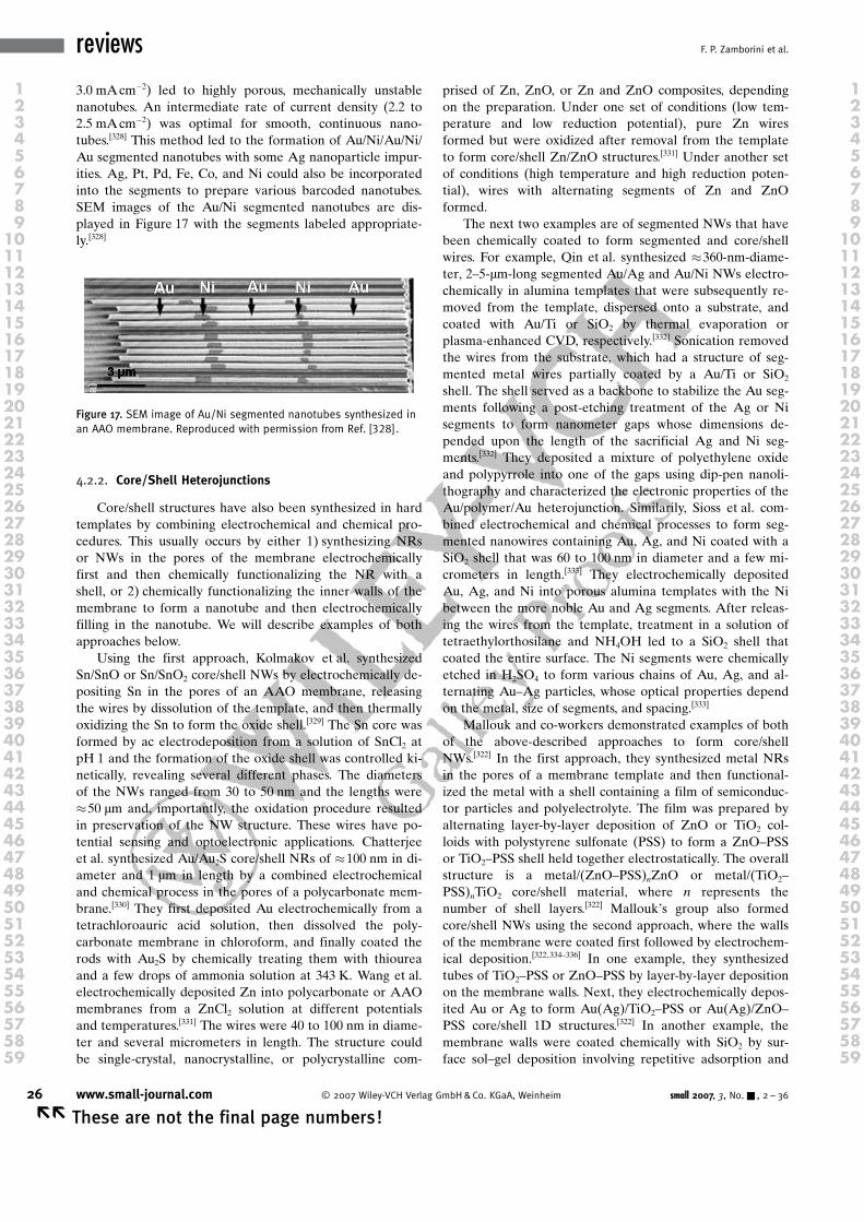
3.0 mAcm�2) led to highly porous, mechanically unstablenanotubes. An intermediate rate of current density (2.2 to2.5 mAcm�2) was optimal for smooth, continuous nano-tubes.[328] This method led to the formation of Au/Ni/Au/Ni/Au segmented nanotubes with some Ag nanoparticle impur-ities. Ag, Pt, Pd, Fe, Co, and Ni could also be incorporatedinto the segments to prepare various barcoded nanotubes.SEM images of the Au/Ni segmented nanotubes are dis-played in Figure 17 with the segments labeled appropriate-ly.[328]
4.2.2. Core/Shell Heterojunctions
Core/shell structures have also been synthesized in hardtemplates by combining electrochemical and chemical pro-cedures. This usually occurs by either 1) synthesizing NRsor NWs in the pores of the membrane electrochemicallyfirst and then chemically functionalizing the NR with ashell, or 2) chemically functionalizing the inner walls of themembrane to form a nanotube and then electrochemicallyfilling in the nanotube. We will describe examples of bothapproaches below.
Using the first approach, Kolmakov et al. synthesizedSn/SnO or Sn/SnO2 core/shell NWs by electrochemically de-positing Sn in the pores of an AAO membrane, releasingthe wires by dissolution of the template, and then thermallyoxidizing the Sn to form the oxide shell.[329] The Sn core wasformed by ac electrodeposition from a solution of SnCl2 atpH 1 and the formation of the oxide shell was controlled ki-netically, revealing several different phases. The diametersof the NWs ranged from 30 to 50 nm and the lengths were�50 mm and, importantly, the oxidation procedure resultedin preservation of the NW structure. These wires have po-tential sensing and optoelectronic applications. Chatterjeeet al. synthesized Au/Au2S core/shell NRs of �100 nm in di-ameter and 1 mm in length by a combined electrochemicaland chemical process in the pores of a polycarbonate mem-brane.[330] They first deposited Au electrochemically from atetrachloroauric acid solution, then dissolved the poly-carbonate membrane in chloroform, and finally coated therods with Au2S by chemically treating them with thioureaand a few drops of ammonia solution at 343 K. Wang et al.electrochemically deposited Zn into polycarbonate or AAOmembranes from a ZnCl2 solution at different potentialsand temperatures.[331] The wires were 40 to 100 nm in diame-ter and several micrometers in length. The structure couldbe single-crystal, nanocrystalline, or polycrystalline com-
prised of Zn, ZnO, or Zn and ZnO composites, dependingon the preparation. Under one set of conditions (low tem-perature and low reduction potential), pure Zn wiresformed but were oxidized after removal from the templateto form core/shell Zn/ZnO structures.[331] Under another setof conditions (high temperature and high reduction poten-tial), wires with alternating segments of Zn and ZnOformed.
The next two examples are of segmented NWs that havebeen chemically coated to form segmented and core/shellwires. For example, Qin et al. synthesized �360-nm-diame-ter, 2–5-mm-long segmented Au/Ag and Au/Ni NWs electro-chemically in alumina templates that were subsequently re-moved from the template, dispersed onto a substrate, andcoated with Au/Ti or SiO2 by thermal evaporation orplasma-enhanced CVD, respectively.[332] Sonication removedthe wires from the substrate, which had a structure of seg-mented metal wires partially coated by a Au/Ti or SiO2
shell. The shell served as a backbone to stabilize the Au seg-ments following a post-etching treatment of the Ag or Nisegments to form nanometer gaps whose dimensions de-pended upon the length of the sacrificial Ag and Ni seg-ments.[332] They deposited a mixture of polyethylene oxideand polypyrrole into one of the gaps using dip-pen nanoli-thography and characterized the electronic properties of theAu/polymer/Au heterojunction. Similarily, Sioss et al. com-bined electrochemical and chemical processes to form seg-mented nanowires containing Au, Ag, and Ni coated with aSiO2 shell that was 60 to 100 nm in diameter and a few mi-crometers in length.[333] They electrochemically depositedAu, Ag, and Ni into porous alumina templates with the Nibetween the more noble Au and Ag segments. After releas-ing the wires from the template, treatment in a solution oftetraethylorthosilane and NH4OH led to a SiO2 shell thatcoated the entire surface. The Ni segments were chemicallyetched in H2SO4 to form various chains of Au, Ag, and al-ternating Au–Ag particles, whose optical properties dependon the metal, size of segments, and spacing.[333]
Mallouk and co-workers demonstrated examples of bothof the above-described approaches to form core/shellNWs.[322] In the first approach, they synthesized metal NRsin the pores of a membrane template and then functional-ized the metal with a shell containing a film of semiconduc-tor particles and polyelectrolyte. The film was prepared byalternating layer-by-layer deposition of ZnO or TiO2 col-loids with polystyrene sulfonate (PSS) to form a ZnO–PSSor TiO2–PSS shell held together electrostatically. The overallstructure is a metal/ACHTUNGTRENNUNG(ZnO–PSS)nZnO or metal/ACHTUNGTRENNUNG(TiO2–PSS)nTiO2 core/shell material, where n represents thenumber of shell layers.[322] MalloukGs group also formedcore/shell NWs using the second approach, where the wallsof the membrane were coated first followed by electrochem-ical deposition.[322,334–336] In one example, they synthesizedtubes of TiO2–PSS or ZnO–PSS by layer-by-layer depositionon the membrane walls. Next, they electrochemically depos-ited Au or Ag to form Au(Ag)/TiO2–PSS or Au(Ag)/ZnO–PSS core/shell 1D structures.[322] In another example, themembrane walls were coated chemically with SiO2 by sur-face sol–gel deposition involving repetitive adsorption and
Figure 17. SEM image of Au/Ni segmented nanotubes synthesized inan AAO membrane. Reproduced with permission from Ref. [328].
26 www.small-journal.com � 2007 Wiley-VCH Verlag GmbH&Co. KGaA, Weinheim small 2007, 3, No.& , 2 – 36
�� These are not the final page numbers!
reviews F. P. Zamborini et al.
1 12 23 34 45 56 67 78 89 9
10 1011 1112 1213 1314 1415 1516 1617 1718 1819 1920 2021 2122 2223 2324 2425 2526 2627 2728 2829 2930 3031 3132 3233 3334 3435 3536 3637 3738 3839 3940 4041 4142 4243 4344 4445 4546 4647 4748 4849 4950 5051 5152 5253 5354 5455 5556 5657 5758 5859 59
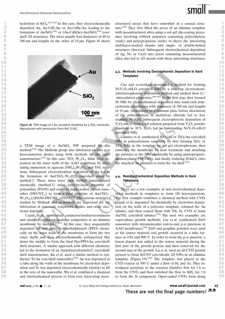
hydrolysis of SiCl4.[334,336] In this case, they electrochemically
deposited Au, Au-CdS-Au, or Au-CdSe-Au, leading to theformation of Au/SiO2
[336] or (Au-CdS(Se)-Au)/SiO2[334] core/
shell 1D structures. The wires usually had diameters of 40 to300 nm and lengths on the order of 10 mm. Figure 18 shows
a TEM image of a Au/SiO2 NW prepared by thismethod.[336] The Mallouk group also fabricated on-wire p–nheterojunction diodes using both methods on the samenanostructure.[335] In this case, TiO2–W12O41 films were de-posited on the inner walls of the AAO membrane by alter-nating immersion in aqueous (NH4)10W12O41 and TiO2 solu-tions. Subsequent electrochemical deposition of Au led tothe formation of Au/(TiO2–W12O41) core/shell wires bymethod 2. These wires were then further functionalizedchemically (method 1) using layer-by-layer assembly ofpolyaniline (PANI) and oxidized single-walled carbon nano-tubes (SWCNTox) to form a final structure of Au/(TiO2–W12O41)3/(PANI-SWCNTox)3PANI.
[335] The various structuresstudied by Mallouk and co-workers are important for thefabrication of nanoscale transistors, diodes, and other elec-tronic functions.
Cepak et al. synthesized conductor/insulator/conductorand insulator/conductor/insulator composites in an aluminamembrane by method 2.[337] In this case, they sequentiallydeposited Au and poly(2,6-dimethylphenol) (PPO) chemi-cally on the inner walls of the membrane to form the twoouter shells and then electrochemically polymerized Ppydown the middle to form the final Ppy/PPO/Au core/shell/shell structure. A similar approach with different chemistryled to the formation of an Au/polyacrylonitrile/C core/shell/shell nanostructure. Ku et al. used a similar method to syn-thesize Te/Au core/shell nanocables.[338] Au was deposited asa tube along the walls of the membrane by electroless depo-sition and Te was deposited electrochemically (slowly) to fillin the core of the nanocable. Wu et al. combined a chemicaland electrochemical process to form very interesting meso-
structured arrays that have somewhat of a coaxial struc-ture.[339] They first filled the pores of an alumina templatewith mesostructured silica using a sol–gel dip-coating proce-dure involving triblock polymers containing poly(ethyleneoxide) and poly(propylene oxide) to direct the interestingmultilayer-stacked donuts and single- or double-helicalstructures observed. Subsequent electrochemical depositionof Ag, Ni, or Cu2O into pores containing mesostructuredsilica also led to 1D metals with these interesting structures.
4.3. Methods Involving Electrophoretic Deposition in HardTemplates
Cao and co-workers developed a method for formingNi/V2O5·nH2O core/shell NRs by a two-step electrochemi-cal/electrophoretic deposition method and studied their Li+
-intercalation properties.[340–342] In the first step, they formedNi NRs by electrochemical deposition into track-etch poly-carbonate membranes with diameters of 200 nm and lengthsof 10 mm. Attachment to a titanium plate before dissolutionof the polycarbonate in methylene chloride led to freestanding Ni NRs. Subsequent electrophoretic deposition ofV2O5·nH2O from a sol solution prepared from V2O5 powderdissolved in 30% H2O2 led to freestanding Ni/V2O5·nH2Ocore/shell NRs.
Limmer et al. synthesized SiO2/Au or TiO2/Au core/shellNRs in polycarbonate templates by first forming SiO2 orTiO2 NRs in the template by sol–gel electrophoresis, thenremoving the membrane by heat treatment and attachingAu particles to the NRs chemically by using aminopropytri-methoxysilane (APTMS), and finally reducing HAuCl4 ontothe attached Au particles to form the Au shell.[343]
4.4. Non-Electrochemical Deposition Methods in HardTemplates
There are a few examples of non-electrochemical depo-sition methods in templates to form 1D heterojunctions.The first example combines a chemical method with CVD.Cepak et al. deposited Au chemically by electroless deposi-tion on the walls of a polyester template, released the Autubules, and then coated them with TiS2 by CVD to formAu/TiS2 core/shell tubules.
[337] The next two examples arevapor-phase growth methods; Liu et al. synthesized ZnOnanowires with intramolecular end-to-end p–n junctions inAAO membranes.[344] ZnO and graphite powders were usedas the source material and growth occurred in a tube fur-nace at 4 Pa and 900 8C. In order to form the p–n junction, aboron dopant was added to the source material during thefirst part of the growth process and then removed for thesecond step of the growth. Lu et al. used an all-CVD growthprocess to form Si/CNT core/sheath 1D NWs in an aluminatemplate (Figure 19).[345] The template was placed in theCVD reactor at 700 8C under a flow of H2 and Ar. They in-troduced acetylene to the reaction chamber first for 1 h toform the CNTs and then switched the flow to SiH4 for 1 hto form the Si component. Open-ended CNTs form along
Figure 18. TEM image of a Au nanowire sheathed by a SiO2 nanotube.Reproduced with permission from Ref. [336].
small 2007, 3, No.& , 2 – 36 � 2007 Wiley-VCH Verlag GmbH&Co. KGaA, Weinheim www.small-journal.com 27
These are not the final page numbers! ��
One-Dimensional Nanoscale Heterojunctions
1 12 23 34 45 56 67 78 89 9
10 1011 1112 1213 1314 1415 1516 1617 1718 1819 1920 2021 2122 2223 2324 2425 2526 2627 2728 2829 2930 3031 3132 3233 3334 3435 3536 3637 3738 3839 3940 4041 4142 4243 4344 4445 4546 4647 4748 4849 4950 5051 5152 5253 5354 5455 5556 5657 5758 5859 59
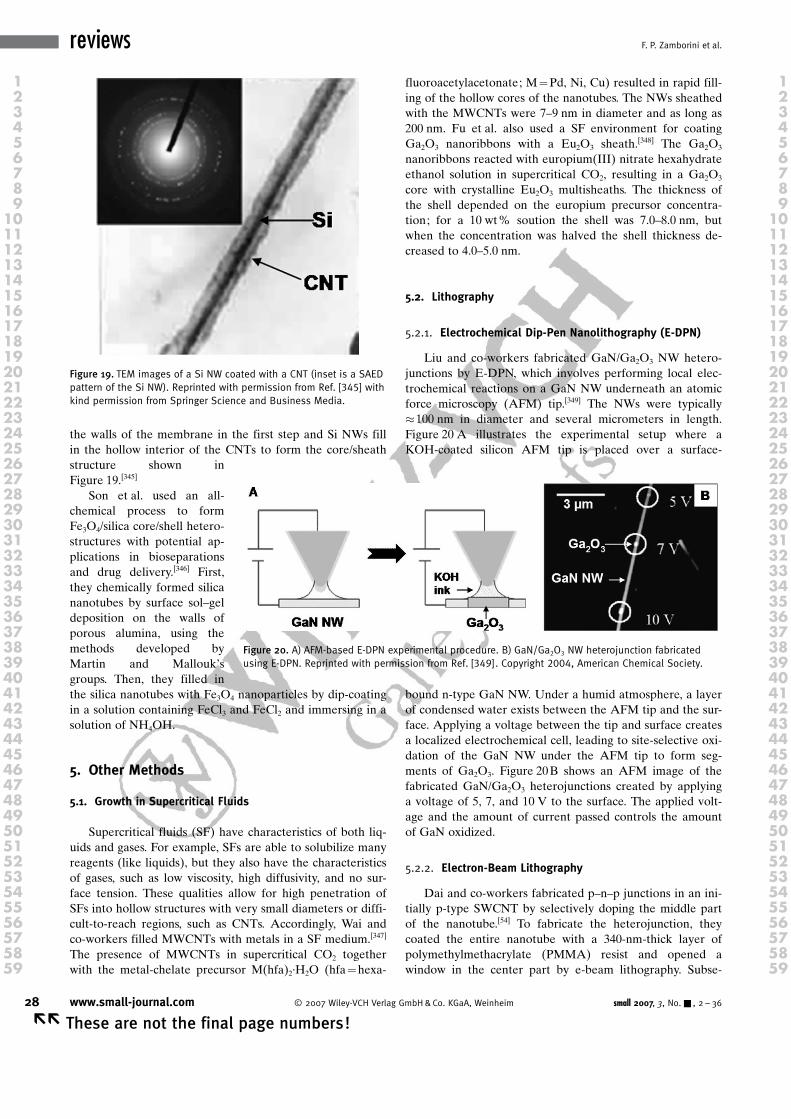
the walls of the membrane in the first step and Si NWs fillin the hollow interior of the CNTs to form the core/sheathstructure shown inFigure 19.[345]
Son et al. used an all-chemical process to formFe3O4/silica core/shell hetero-structures with potential ap-plications in bioseparationsand drug delivery.[346] First,they chemically formed silicananotubes by surface sol–geldeposition on the walls ofporous alumina, using themethods developed byMartin and MalloukGsgroups. Then, they filled inthe silica nanotubes with Fe3O4 nanoparticles by dip-coatingin a solution containing FeCl3 and FeCl2 and immersing in asolution of NH4OH.
5. Other Methods
5.1. Growth in Supercritical Fluids
Supercritical fluids (SF) have characteristics of both liq-uids and gases. For example, SFs are able to solubilize manyreagents (like liquids), but they also have the characteristicsof gases, such as low viscosity, high diffusivity, and no sur-face tension. These qualities allow for high penetration ofSFs into hollow structures with very small diameters or diffi-cult-to-reach regions, such as CNTs. Accordingly, Wai andco-workers filled MWCNTs with metals in a SF medium.[347]
The presence of MWCNTs in supercritical CO2 togetherwith the metal-chelate precursor MACHTUNGTRENNUNG(hfa)2·H2O (hfa=hexa-
fluoroacetylacetonate; M=Pd, Ni, Cu) resulted in rapid fill-ing of the hollow cores of the nanotubes. The NWs sheathedwith the MWCNTs were 7–9 nm in diameter and as long as200 nm. Fu et al. also used a SF environment for coatingGa2O3 nanoribbons with a Eu2O3 sheath.
[348] The Ga2O3
nanoribbons reacted with europium ACHTUNGTRENNUNG(III) nitrate hexahydrateethanol solution in supercritical CO2, resulting in a Ga2O3
core with crystalline Eu2O3 multisheaths. The thickness ofthe shell depended on the europium precursor concentra-tion; for a 10 wt% soution the shell was 7.0–8.0 nm, butwhen the concentration was halved the shell thickness de-creased to 4.0–5.0 nm.
5.2. Lithography
5.2.1. Electrochemical Dip-Pen Nanolithography (E-DPN)
Liu and co-workers fabricated GaN/Ga2O3 NW hetero-junctions by E-DPN, which involves performing local elec-trochemical reactions on a GaN NW underneath an atomicforce microscopy (AFM) tip.[349] The NWs were typically�100 nm in diameter and several micrometers in length.Figure 20 A illustrates the experimental setup where aKOH-coated silicon AFM tip is placed over a surface-
bound n-type GaN NW. Under a humid atmosphere, a layerof condensed water exists between the AFM tip and the sur-face. Applying a voltage between the tip and surface createsa localized electrochemical cell, leading to site-selective oxi-dation of the GaN NW under the AFM tip to form seg-ments of Ga2O3. Figure 20B shows an AFM image of thefabricated GaN/Ga2O3 heterojunctions created by applyinga voltage of 5, 7, and 10 V to the surface. The applied volt-age and the amount of current passed controls the amountof GaN oxidized.
5.2.2. Electron-Beam Lithography
Dai and co-workers fabricated p–n–p junctions in an ini-tially p-type SWCNT by selectively doping the middle partof the nanotube.[54] To fabricate the heterojunction, theycoated the entire nanotube with a 340-nm-thick layer ofpolymethylmethacrylate (PMMA) resist and opened awindow in the center part by e-beam lithography. Subse-
Figure 19. TEM images of a Si NW coated with a CNT (inset is a SAEDpattern of the Si NW). Reprinted with permission from Ref. [345] withkind permission from Springer Science and Business Media.
Figure 20. A) AFM-based E-DPN experimental procedure. B) GaN/Ga2O3 NW heterojunction fabricatedusing E-DPN. Reprinted with permission from Ref. [349]. Copyright 2004, American Chemical Society.
28 www.small-journal.com � 2007 Wiley-VCH Verlag GmbH&Co. KGaA, Weinheim small 2007, 3, No.& , 2 – 36
�� These are not the final page numbers!
reviews F. P. Zamborini et al.
1 12 23 34 45 56 67 78 89 9
10 1011 1112 1213 1314 1415 1516 1617 1718 1819 1920 2021 2122 2223 2324 2425 2526 2627 2728 2829 2930 3031 3132 3233 3334 3435 3536 3637 3738 3839 3940 4041 4142 4243 4344 4445 4546 4647 4748 4849 4950 5051 5152 5253 5354 5455 5556 5657 5758 5859 59
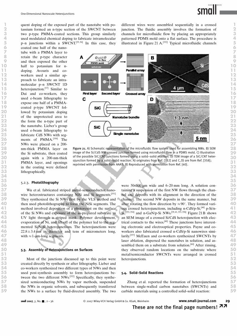
quent doping of the exposed part of the nanotube with po-tassium formed an n-type section of the SWCNT betweentwo p-type PMMA-coated sections. This group similarlyused modulated chemical doping to fabricate intramolecularp–n junctions within a SWCNT.[55,56] In this case, theycoated one half of the nano-tube with a PMMA layer toretain the p-type characterand then exposed the otherhalf to potassium for n-doping. Avouris and co-workers used a similar ap-proach to fabricate an intra-molecular p–n SWCNT 1Dheterojunction.[57] Similar toDai and co-workers, theyused e-beam lithography toexpose one half of a PMMA-coated p-type SWCNT fol-lowed by potassium dopingof the unprotected area tothe form the n-type part ofthe nanotube. LieberGs groupused e-beam lithography tofabricate CdS NWs with seg-ments of PMMA.[350] TheNWs were placed on a 200-nm-thick PMMA layer onthe Si substrate, then coatedagain with a 200-nm-thickPMMA layer, and openingsin the coating were definedlithographically.
5.2.3. Photolithography
Wu et al. fabricated striped metal–semiconductor nano-wire heterostructures containing NiSi and Si segments.[351]
They synthesized the Si NWs first by the VLS method andthen used photolithography to form the NiSi segments. Themethod involved deposition of a photoresist on the surfaceof the Si NWs and exposure of the as-prepared substrate toUV light through a striped mask. Polymer development,evaporation of Ni, and lift-off of the polymer led to the seg-mented Si/NiSi heterojunctions. The heterojunctions were22.8�3.4 nm in diameter and tens of micrometers long,with �1-mm-long segments.
5.3. Assembly of Heterojunctions on Surfaces
Most of the junctions discussed up to this point werecreated directly by synthesis or after lithography. Lieber andco-workers synthesized two different types of NWs and thenused post-synthesis assembly to form heterojunctions be-tween the two different NWs.[352] Specifically, they synthe-sized semiconducting NWs by vapor methods, suspendedthe NWs in organic solvents, and subsequently transferredthe NWs to a surface by fluid-directed assembly. The two
different wires were assembled sequentially in a crossedjunction. The fluidic assembly involves the formation ofchannels for microfluidic flow by placing an appropriatelypatterned PDMS mold onto a flat surface. The procedure isillustrated in Figure 21 A.[352] Typical microfluidic channels
were 50–500 mm wide and 6–20 mm long. A solution con-taining a suspension of the first NW flows through the chan-nel and deposits with its alignment in the direction of thechannel. The second NW deposits in the same manner, butafter rotating the flow direction by �908. They formed vari-ous crossed heterojunctions, including n-CdS/p-Si,[40] p-Si/n-Si,[353,354] and n-GaN/p-Si NWs.[39,41,355,356] Figure 21B showsan SEM image of a crossed Si/CdS heterojunction with elec-trical contacts to the wires.[40] These junctions have interest-ing electronic and electrooptical properties. Payne and co-workers also fabricated crossed n-CdS/p-Si nanowires simi-larily.[357] McEuen and co-workers synthesized SWCNTs bylaser ablation, dispersed the nanotubes in solution, and as-sembled them on a substrate from solution.[60] After rinsing,they observed random locations on the substrate wheremetal/semiconductor SWCNTs were arranged in crossedheterojunctions.
5.4. Solid–Solid Reactions
Zhang et al. reported the formation of heterojunctionsbetween single-walled carbon nanotubes (SWCNTs) andcarbide materials using a controlled solid–solid reaction:
Figure 21. A) Schematic representation of the microfluidic flow system used for assembling NWs. B) SEMimage of the Si/CdS NW crossed junction formed using microfluidic flow in a PDMS mold. C) Illustrationof the possible SiC/CNT junctions formed using a solid–solid reaction. D) TEM image of a SiC/CNT heter-ojunction formed by a solid–solid reaction. A) originates from Ref. [352] and C,D) are from Ref. [358];reprinted with permission from AAAS. B) Reproduced with permission from Ref. [40].
small 2007, 3, No.& , 2 – 36 � 2007 Wiley-VCH Verlag GmbH&Co. KGaA, Weinheim www.small-journal.com 29
These are not the final page numbers! ��
One-Dimensional Nanoscale Heterojunctions
1 12 23 34 45 56 67 78 89 9
10 1011 1112 1213 1314 1415 1516 1617 1718 1819 1920 2021 2122 2223 2324 2425 2526 2627 2728 2829 2930 3031 3132 3233 3334 3435 3536 3637 3738 3839 3940 4041 4142 4243 4344 4445 4546 4647 4748 4849 4950 5051 5152 5253 5354 5455 5556 5657 5758 5859 59
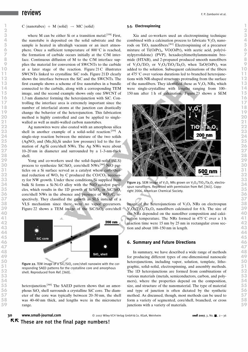
C ðnanotubesÞ þ M ðsolidÞ ! MC ðsolidÞ
where M can be either Si or a transition metal.[358] First,the nanotube is deposited on the solid substrate and thesample is heated in ultrahigh vacuum or an inert atmos-phere. Once a sufficient temperature of 800 8C is reached,the formation of carbide occurs initially at the C/M inter-face. Continuous diffusion of M to the C/M interface sup-plies the material for conversion of SWCNTs to the carbideat a later stage of the reaction. Figure 21C illustratesSWCNTs linked to crystalline SiC rods. Figure 21D clearlyshows the interface between the SiC and the SWCNTs. Thefirst example shows a scheme of five nanotubes in a bundleconnected to the carbide, along with a corresponding TEMimage, and the second example shows only one SWCNT of1.3 nm diameter forming the heterojunction with SiC. Con-trolling the interface area is extremely important since thenumber of interfacial atoms at the junction can drasticallychange the behavior of the heterojunction. This fabricationmethod is highly controlled and can be applied to single-walled as well as multi-walled carbon nanotubes.
Ag nanowires were also coated with an amorphous silicashell in another example of a solid–solid reaction.[359] Asingle-step reaction between the mixture of the two solids(AgNO3 and (Me3Si)4Si under low pressure) led to the for-mation of Ag/Si core/shell NWs. The Ag NWs were about10–20 nm in diameter and surrounded by a 1–3-nm-thickshell.
Yong and co-workers used the solid–liquid–solid (SLS)process to synthesize SiC/SiOx core/shell NWs.
[360] NiO par-ticles on a Si surface served as a catalyst where carbother-mal reduction of WO3 by C produced the CO/CO2 necessa-ry for NW growth. Under these conditions, Si supplied frombulk Si forms a Si-Ni-O alloy with the NiO catalyst parti-cles, which results in the 1D growth of Si/SiOx or SiC/SiOx
core/shell NWs in the absence and presence of WO3/C, re-spectively. They classified the growth as SLS instead of aVLS mechanism since there were no vapor precursors.Figure 22 shows a TEM image of the SiC/SiOx core/shell
heterojunction.[360] The SAED pattern shows that an amor-phous SiOx shell surrounds a crystalline SiC core. The diam-eter of the core was typically between 20–50 nm, the shellwas 40–60 nm thick, and lengths were in the micrometerrange.
5.5. Electrospinning
Xia and co-workers used an electrospinning techniquecombined with a calcination process to fabricate V2O5 nano-rods on TiO2 nanofibers.
[361] Electrospinning of a precursormixture of TiACHTUNGTRENNUNG(OiPr)4, VOACHTUNGTRENNUNG(OiPr)3 with acetic acid, poly(vi-nylpyrrolidone) (PVP), hexadecyltimethylammonuim bro-mide (HTAB), and 2-propanol produced smooth nanofibersof V2O5/TiO2 or V2O5/TiO2/Ta2O5 when TaO ACHTUNGTRENNUNG(OiPr)3 wasadded to the solution. Subsequent calcinations of the fibersat 475 8C over various durations led to branched heterojunc-tions with NR-shaped structures protruding from the surfaceof the nanofibers. They identified these as V2O5 NRs, whichwere single-crystalline with lengths ranging from 100–150 nm after 1 h of calcination. Figure 23 shows a SEM
image of the heterojunctions of V2O5 NRs on electrospunV2O5/TiO2/Ta2O3 nanofibers calcinated for 6 h. The size ofthe NRs depended on the nanofiber composition and calci-nation temperature. The NRs formed in 475 8C over a 1 hreaction time were 15 nm by 25 nm in rectangular cross sec-tion and about 100–150 nm in length.
6. Summary and Future Directions
In summary, we have described a wide range of methodsfor producing different types of one-dimensional nanoscaleheterojunctions, including vapor, solution, template, litho-graphic, solid–solid, electrospinning, and assembly methods.The 1D heterojunctions are formed from combinations ofvarious materials (metals, semiconductors, carbon, and poly-mers), where the properties depend on the composition,size, and structure of the nanomaterial. The type of materialand type of junction is often dictated by the syntheticmethod. As discussed, though, most methods can be used toform a variety of segmented, core/shell, branched, or crossjunctions with a variety of materials.
Figure 22. TEM image of a SiC/SiOx core/shell nanowire with the cor-responding SAED patterns for the crystalline core and amorphousshell. Reproduced from Ref. [360].
Figure 23. SEM image of V2O5 NRs grown on V2O5/TiO2/Ta2O5 electro-spun nanofibers. Reprinted with permission from Ref. [361]. Copy-right 2006, American Chemical Society.
30 www.small-journal.com � 2007 Wiley-VCH Verlag GmbH&Co. KGaA, Weinheim small 2007, 3, No.& , 2 – 36
�� These are not the final page numbers!
reviews F. P. Zamborini et al.
1 12 23 34 45 56 67 78 89 9
10 1011 1112 1213 1314 1415 1516 1617 1718 1819 1920 2021 2122 2223 2324 2425 2526 2627 2728 2829 2930 3031 3132 3233 3334 3435 3536 3637 3738 3839 3940 4041 4142 4243 4344 4445 4546 4647 4748 4849 4950 5051 5152 5253 5354 5455 5556 5657 5758 5859 59
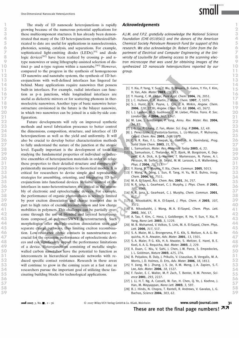
The study of 1D nanoscale heterojunctions is rapidlygrowing because of the numerous potential applications forthese multicomponent stuctures. It has already been demon-strated that many of the 1D heterojunctions synthesized/fab-ricated to date are useful for applications in nanoelectronics,photonics, sensing, catalysis, and separations. For example,sophisticated light-emitting diodes (LEDs),[93] and diodelogic devices[362] have been realized by crossing p- and n-type nanowires or using lithography-assisted selection of dis-tinct p- and n-type regions within a nanotube.[363] However,compared to the progress in the synthesis of homogeneous1D nanowire and nanotube systems, the synthesis of 1D het-erojunctions with well-defined interfaces has lingered farbehind. Many applications require nanowires that possessbuilt-in interfaces. For example, radial interfaces can func-tion as p–n junctions, while longitudinal interfaces areuseful as dielectric mirrors or for scattering phonons in ther-moelectric nanowires. Another type of basic nanowire heter-ostructure envisioned in the future is the bilayer nanowire,in which two nanowires can be joined in a side-by-side con-figuration.
Future developments will rely on improved syntheticmethods and novel fabrication processes to better controlthe dimensions, composition, structure, and interface of 1Dheterojunctions as well as the yield and uniformity. It willalso be crucial to develop better characterization methodsto fully understand the nature of the junction at the atomiclevel. Equally important is the development of tools forstudying the fundamental properties of individual or collec-tive ensembles of heterojunction materials in order to relatethese properties to their detailed structure and compare ex-perimentally measured properties to theoretical models. It iscritical for researchers to devise simple and reproduciblestrategies for assembling, orienting, and integrating 1D het-erojunctions into functional devices. Reliable control of theinterfaces in nano-heterostructures are critical in the assem-bly of electronic and optoelectronic devices. For example,the performance of organic photovoltaics is severely limitedby poor exciton dissociation and charge transport due inpart to high rates of exciton recombination and low chargemobilities in polymers. This challenge can be partially over-come through the use of blended and layered heterojunc-tions composed of polymer/SWNT heterostructures. Suchmorphologies offer multiple-exciton dissociation sites andseparate charge pathways, thus limiting exciton recombina-tion. Low-resistance ohmic contacts in nanostructures arecrucial for the optimum performance of optoelectronic devi-ces and can significantly impact the performance limitationsof a device. Heterojunctions consisting of metallic single-walled carbon nanotubes have the potential to function asinterconnects in hierarchical nanoscale networks with re-duced specific contact resistance. Research in these areaswill continue to grow in the coming years at a fast rate asresearchers pursue the important goal of utilizing these fas-cinating building blocks for technological applications.
Acknowledgements
A.J.M. and F.P.Z. gratefully acknowledge the National ScienceFoundation (CHE-0518561) and the donors of the AmericanChemical Society Petroleum Research Fund for support of thisresearch. We also acknowledge Dr. Robert Cohn from the De-partment of Electrical and Computer Engineering at the Uni-versity of Louisville for allowing access to the scanning elec-tron microscope that was used for obtaining images of thesynthesized 1D nanoscale heterojunctions reported by ourgroup.
[1] Y. Xia, P. Yang, Y. Sun, Y. Wu, B. Mayers, B. Gates, Y. Yin, F. Kim,H. Yan, Adv. Mater. 2003, 15, 353.
[2] Y. Huang, C. M. Lieber, Pure Appl. Chem. 2004, 76, 2051.[3] J. C. Hulteen, C. R. Martin, J. Mater. Chem. 1997, 7, 1075.[4] S. J. Hurst, E. K. Payne, L. Qin, C. A. Mirkin, Angew. Chem.
2006, 118, 2738; Angew. Chem. Int. Ed. 2006, 45, 2672.[5] L. J. Lauhon, M. S. Gudiksen, C. M. Lieber, Philos. Trans. R. Soc.
London Ser. A 2004, 362, 1247.[6] M. Law, J. Goldberger, P. Yang, Annu. Rev. Mater. Res. 2004,
34, 83.[7] J. G. Lu, P. Chang, Z. Fan, Mater. Sci. Eng. R 2006, 52, 49.[8] J. Perez-Juste, I. Pastoriza-Santos, L. Liz-Marzan, P. Mulvaney,
Coord. Chem. Rev. 2005, 249, 1870.[9] C. N. R. Rao, F. L. Deepak, G. Gundiah, A. Govindaraj, Prog.
Solid State Chem. 2003, 31, 5.[10] L. Samuelson, Mater. Res. Materials Today 2003, 6, 22.[11] L. Samuelson, C. Thelander, M. T. Bjork, M. Borgstrom, K. Dep-
pert, K. A. Dick, A. E. Hansen, T. Martensson, N. Panev, A. I.Persson, W. Seifert, N. Skold, M. W. Larsson, L. R. Wallenberg,Phys. E 2004, 25, 313.
[12] Y. Xiong, B. T. Mayers, Y. Xia, Chem. Commun. 2005, 5013.[13] F. Wang, A. Dong, J. Sun, R. Tang, H. Yu, W. E. Buhro, Inorg.
Chem. 2006, 45, 7511.[14] M. A. El-Sayed, Acc. Chem. Res. 2001, 34, 257.[15] N. R. Jana, L. Gearheart, C. J. Murphy, J. Phys. Chem. B 2001,
105, 4065.[16] N. R. Jana, L. Gearheart, C. J. Murphy, Chem. Commun. 2001,
617.[17] B. Nikoobakht, M. A. El-Sayed, J. Phys. Chem. A 2003, 107,
3372.[18] B. Nikoobakht, J. Wang, M. A. El-Sayed, Chem. Phys. Lett.
2002, 366, 17.[19] A. Tao, F. Kim, C. Hess, J. Goldberger, R. He, Y. Sun, Y. Xia, P.
Yang, Nano Lett. 2003, 3, 1229.[20] M. B. Mohamed, V. Volkov, S. Link, M. A. El-Sayed, Chem. Phys.
Lett. 2000, 317, 517.[21] S. A. Maier, M. L. Brongersma, P. G. Kik, S. Meltzer, A. A. G. Re-
quicha, H. A. Atwater, Adv. Mater. 2001, 13, 1501.[22] S. A. Maier, P. G. Kik, H. A. Atwater, S. Meltzer, E. Harel, B. E.
Koel, A. A. G. Requicha, Nat. Mater. 2003, 2, 229.[23] X. Duan, C. Niu, V. Sahi, J. Chen, J. W. Parce, S. Empedocles,
J. L. Goldman, Nature 2003, 425, 274.[24] B. Polyakov, B. Daly, J. Prikulis, V. Lisauskas, B. Vengalis, M. A.
Morris, J. D. Holmes, D. Erts, Adv. Mater. 2006, 18, 1812.[25] Y. Jiang, W. J. Zhang, J. S. Jie, X. M. Meng, J. A. Zapien, S.-T.
Lee, Adv. Mater. 2006, 18, 1527.[26] F. Favier, E. C. Walter, M. P. Zach, T. Benter, R. M. Penner, Sci-
ence 2001, 293, 2227.[27] J. Li, H. T. Ng, A. Cassell, W. Fan, H. Chen, Q. Ye, J. Koehne, J.
Han, M. Meyyappan, Nano Lett. 2003, 3, 597.[28] B. J. Hinds, N. Chopra, T. Rantell, R. Andrews, V. Gavalas, L. G.
Bachas, Science 2004, 303, 62.
small 2007, 3, No.& , 2 – 36 � 2007 Wiley-VCH Verlag GmbH&Co. KGaA, Weinheim www.small-journal.com 31
These are not the final page numbers! ��
One-Dimensional Nanoscale Heterojunctions
1 12 23 34 45 56 67 78 89 9
10 1011 1112 1213 1314 1415 1516 1617 1718 1819 1920 2021 2122 2223 2324 2425 2526 2627 2728 2829 2930 3031 3132 3233 3334 3435 3536 3637 3738 3839 3940 4041 4142 4243 4344 4445 4546 4647 4748 4849 4950 5051 5152 5253 5354 5455 5556 5657 5758 5859 59
[29] H. W. C. Postma, T. Teepen, Z. Yao, M. Grifoni, C. Dekker, Sci-ence 2001, 293, 76.
[30] R. Martel, T. Schmidt, H. R. Shea, T. Hertel, P. Avouris, Appl.Phys. Lett. 1998, 73, 2447.
[31] Y. Cui, Z. Zhong, D. Wang, W. U. Wang, C. M. Lieber, Nano Lett.2003, 3, 149.
[32] G. Zheng, W. Lu, S. Jin, C. M. Lieber, Adv. Mater. 2004, 16,1890.
[33] Y. Cui, Q. Wei, H.-Y. Park, C. M. Lieber, Science 2001, 293,1289.
[34] J.-i. Hahm, C. M. Lieber, Nano Lett. 2004, 4, 51.[35] J. Kong, H. Dai, J. Phys. Chem. B 2001, 105, 2890.[36] J. Wang, M. S. Gudiksen, X. Duan, Y. Cui, C. M. Lieber, Science
2001, 293, 1455.[37] X. Duan, Y. Huang, Y. Cui, J. Wang, C. M. Lieber, Nature 2001,
409, 66.[38] A. Bogozi, O. Lam, H. He, C. Li, N. J. Tao, L. A. Nagahara, I.
Amlani, R. Tsui, J. Am. Chem. Soc. 2001, 123, 4585.[39] Y. Huang, X. Duan, Y. Cui, C. M. Lieber, Nano Lett. 2002, 2,
101.[40] O. Hayden, R. Agarwal, C. M. Lieber, Nat. Mater. 2006, 5, 352.[41] M. C. McAlpine, R. S. Friedman, C. M. Lieber, Proc. IEEE 2005,
93, 1357.[42] S. G. Penn, L. He, M. J. Natan, Curr. Opin. Chem. Biol. 2003, 7,
609.[43] A. K. Salem, P. C. Searson, K. W. Leong, Nat. Mater. 2003, 2,
668.[44] K.-B. Lee, S. Park, C. A. Mirkin, Angew. Chem. 2004, 116,
3110; Angew. Chem. Int. Ed. 2004, 43, 3048. .[45] F. Liu, J. Y. Lee, W. J. Zhou, Small 2006, 2, 121.[46] S. Park, J.-H. Lim, S.-W. Chung, C. A. Mirkin, Science 2004,
303, 348.[47] A. K. Salem, M. Chen, J. Hayden, K. W. Leong, P. C. Searson,
Nano Lett. 2004, 4, 1163.[48] J. W. Matthews, A. E. Blakeslee, J. Cryst. Growth 1974, 27, 118.[49] L. Zhao, L. Gao, J. Mater. Chem. 2004, 14, 1001.[50] D. G. Ramlan, S. J. May, J.-G. Zheng, J. E. Allen, B. W. Wessels,
L. J. Lauhon, Nano Lett. 2006, 6, 50.[51] J. K. N. Mbindyo, T. E. Mallouk, J. B. Mattzela, I. Kratochvilova,
B. Razavi, T. N. Jackson, T. S. Mayer, J. Am. Chem. Soc. 2002,124, 4020.
[52] J. Zhan, Y. Bando, J. Hu, D. Golberg, K. Kurashima, Small 2006,2, 62.
[53] S. Mather, H. Shen, V. Sivakov, U. Werner, Chem. Mater. 2004,16, 2449.
[54] J. Kong, J. Cao, H. Dai, E. Anderson, Appl. Phys. Lett. 2002, 80,73.
[55] C. Zhou, J. Kong, E. Yenilmez, H. Dai, Science 2000, 290, 1552.[56] A. Javey, R. Tu, D. B. Farmer, J. Guo, R. G. Gordon, H. Dai, Nano
Lett. 2005, 5, 345.[57] V. Derycke, R. Martel, J. Appenzeller, P. Avouris, Nano Lett.
2001, 1, 453.[58] C. Yang, Z. Zhong, C. M. Lieber, Science 2005, 310, 1304.[59] E. Tutuc, J. Appenzeller, M. C. Reuter, S. Guha, Nano Lett.
2006, 6, 2070.[60] M. S. Fuhrer, J. NygJrd, L. Shih, M. Forero, Y.-G. Yoon, M. S. C.
Mazzoni, H. J. Choi, J. Ihm, S. G. Louie, A. Zettl, P. L. McEuen,Science 2000, 288, 494.
[61] Y. Wu, R. Fan, P. Yang, Nano Lett. 2002, 2, 83.[62] N. D. Zakharov, P. Werner, G. Gerth, L. Schubert, L. Sokolov, U.
Gçsele, J. Cryst. Growth 2006, 290, 6.[63] M. S. Gudiksen, L. J. Lauhon, J. Wang, D. C. Smith, C. M. Lieber,
Nature 2002, 415, 617.[64] C. Yang, C. J. Barrelet, F. Capasso, C. M. Lieber, Nano Lett.
2006, 6, 2929.[65] M. T. Bjçrk, C. Thelander, A. E. Hansen, L. E. Jensen, M.W. Lars-
son, L. R. Wallenberg, L. Samuelson, Nano Lett. 2004, 4, 1621.
[66] C. Thelander, M. T. Bjçrk, M. W. Larsson, A. E. Hansen, L. R.Wallenberg, L. Samuelson, Solid State Commun. 2004, 131,573.
[67] C. Thelander, H. A. Nilsson, L. E. Jensen, L. Samuelson, NanoLett. 2005, 5, 635.
[68] M. T. Bjçrk, B. J. Ohlsson, T. Sass, A. I. Persson, C. Thelander,M. H. Magnusson, K. Deppert, L. R. Wallenberg, L. Samuelson,Nano Lett. 2002, 2, 87.
[69] M. T. Bjçrk, B. J. Ohlsson, T. Sass, A. I. Persson, C. Thelander,M. H. Magnusson, K. Deppert, L. R. Wallenberg, L. Samuelson,Appl. Phys. Lett. 2002, 80, 1058.
[70] A. I. Persson, M. T. Bjçrk, S. Jeppesen, J. B. Wagner, L. R. Wal-lenberg, L. Samuelson, Nano Lett. 2006, 6, 403.
[71] M. T. Bjçrk, B. J. Ohlsson, C. Thelander, A. I. Persson, K. Dep-pert, L. R. Wallenberg, L. Samuelson, Appl. Phys. Lett. 2002,81, 4458.
[72] W. Seifert, M. Borgstrom, K. Deppert, K. A. Dick, J. Johansson,M.W. Larsson, T. MJrtensson, N. Skold, C. P. T. Svensson, B. A.Wacaser, L. R. Wallenberg, L. Samuelson, J. Cryst. Growth2004, 272, 211.
[73] T. MJrtensson, C. P. T. Svensson, B. A. Wacaser, M. W. Larsson,W. Seifert, K. Deppert, A. Gustafsson, L. R. Wallenberg, L. Sa-muelson, Nano Lett. 2004, 4, 1987.
[74] H. Pettersson, J. TrLgJrdh, A. I. Persson, L. Landin, D. Hessman,L. Samuelson, Nano Lett. 2006, 6, 229.
[75] B. J. Ohlsson, M. T. Bjçrk, A. I. Persson, C. Thelander, L. R. Wal-lenberg, M. H. Mangusson, K. Deppert, L. Samuelson, Phys. E2002, 13, 1126.
[76] E. Lind, A. I. Persson, L. Samuelson, L.-E. Wernersson, NanoLett. 2006, 6, 1842.
[77] M. A. Verheijen, G. Immink, T. de Smet, M. T. Borgstrom,E. P. A. M. Bakkers, J. Am. Chem. Soc. 2006, 128, 1353.
[78] J. Su, G. Cui, M. Gherasimova, H. Tsukamoto, J. Han, D. Ciu-paru, S. Lim, L. Pfefferle, Y. He, A. V. Nurmikko, C. Broadbridge,A. Lehman, Appl. Phys. Lett. 2005, 86, 013105.
[79] Z.-H. Lan, C.-H. Liang, C.-W. Hsu, C.-T. Wu, H.-M. Lin, S. Dhara,K.-H. Chen, L.-C. Chen, C.-C. Chen, Adv. Funct. Mater. 2004, 14,233.
[80] K. A. Dick, K. Deppert, M. W. Larsson, T. MJrtensson, W. Seifert,L. R. Wallenberg, L. Samuelson, Nat. Mater. 2004, 3, 380.
[81] S. Y. Bae, H. W. Seo, H. C. Choi, J. Park, J. Park, J. Phys. Chem. B2004, 108, 12318.
[82] J. Hu, M. Ouyang, P. Yang, C. M. Lieber, Nature 1999, 399, 48.[83] A. D. Lazareck, T.-F. Kuo, J. M. Xu, B. J. Taft, S. O. Kelley, S. G.
Cloutier, Appl. Phys. Lett. 2006, 89, 103109.[84] A. D. Lazareck, S. G. Cloutier, T.-F. Kuo, B. J. Taft, S. O. Kelley,
J. M. Xu, Nanotechnology 2006, 17, 2661.[85] A. J. Mieszawska, R. Jalilian, G. U. Sumanasekera, F. P. Zambor-
ini, J. Am. Chem. Soc. 2005, 127, 10822.[86] J. X. Wang, H. Y. Chen, Y. Gao, D. F. Liu, L. Song, Z. X. Zhang,
X. W. Zhao, X. Y. Dou, S. D. Luo, W. Y. Zhou, G. Wang, S. S. Xie,J. Cryst. Growth 2005, 284, 73.
[87] H. Kohno, S. Takeda, Appl. Phys. Lett. 2003, 83, 1202.[88] C. W. Na, S. Y. Bae, J. Park, J. Phys. Chem. B 2005, 109,
12785.[89] J. Jie, G. Wang, X. Han, J. G. Hou, J. Phys. Chem. B 2004, 108,
17027.[90] L. J. Lauhon, M. S. Gudiksen, D. Wang, C. M. Lieber, Nature
2002, 420, 57.[91] J. Xiang, W. Lu, Y. Hu, Y. Wu, H. Yan, C. M. Lieber, Nature 2006,
441, 489.[92] W. Lu, J. Xiang, B. P. Timko, Y. Wu, C. M. Lieber, Proc. Natl.
Acad. Sci. USA 2005, 102, 10046.[93] F. Qian, S. Gradecak, Y. Li, C.-Y. Wen, C. M. Lieber, Nano Lett.
2005, 5, 2287.[94] F. Qian, Y. Li, S. Gradecak, D. Wang, C. J. Barrelet, C. M. Lieber,
Nano Lett. 2004, 4, 1975.
32 www.small-journal.com � 2007 Wiley-VCH Verlag GmbH&Co. KGaA, Weinheim small 2007, 3, No.& , 2 – 36
�� These are not the final page numbers!
reviews F. P. Zamborini et al.
1 12 23 34 45 56 67 78 89 9
10 1011 1112 1213 1314 1415 1516 1617 1718 1819 1920 2021 2122 2223 2324 2425 2526 2627 2728 2829 2930 3031 3132 3233 3334 3435 3536 3637 3738 3839 3940 4041 4142 4243 4344 4445 4546 4647 4748 4849 4950 5051 5152 5253 5354 5455 5556 5657 5758 5859 59
[95] Y. Li, J. Xiang, F. Qian, S. Gradecak, Y. Wu, H. Yan, D. A. Blom,C. M. Lieber, Nano Lett. 2006, 6, 1468.
[96] A. B. Greytak, L. J. Lauhon, M. S. Gudiksen, C. M. Lieber, Appl.Phys. Lett. 2004, 84, 4176.
[97] N. Skçld, L. S. Karlsson, M.W. Larsson, M.-E. Pistol, W. Seifert,J. TrLgJrdh, L. Samuelson, Nano Lett. 2005, 5, 1943.
[98] N. Skçld, J. B. Wagner, G. Karlsson, T. HernNn, W. Seifert, M.-E.Pistol, L. Samuelson, Nano Lett. 2006, 6, 2743.
[99] B. Ha, H. C. Kim, S.-G. Kang, Y. H. Kim, J. Y. Lee, C. Y. Park, C. J.Lee, Chem. Mater. 2005, 17, 5398.
[100] B.-K. Kim, J.-J. Kim, J.-O. Lee, K.-j. Kong, H. J. Seo, C. J. Lee,Phys. Rev. B 2005, 71, 153313.
[101] K.-W. Chang, J.-J. Wu, Adv. Mater. 2005, 17, 241.[102] K.-W. Chang, J.-J. Wu, J. Phys. Chem. B 2005, 109, 13572.[103] L. Zhang, R. Tu, H. Dai, Nano Lett. 2006, 6, 2785.[104] H.-M. Lin, Y.-L. Chen, J. Yang, Y.-C. Liu, K.-M. Yin, J.-J. Kai, F.-R.
Chen, L.-C. Chen, C.-C. Chen, Nano Lett. 2003, 3, 537.[105] Y. Wu, P. Yang, Appl. Phys. Lett. 2000, 77, 43.[106] Y. Wu, P. Yang, Adv. Mater. 2001, 13, 520.[107] C.-C. Chen, C.-C. Yeh, C.-H. Liang, C.-C. Lee, C.-H. Chen, M.-Y.
Yu, H.-L. Liu, L. C. Chen, Y.-S. Lin, K.-J. Ma, K. H. Chen, J. Phys.Chem. Solids 2001, 62, 1577.
[108] L. W. Yin, Y. Bando, Y. C. Zhu, M. S. Li, Appl. Phys. Lett. 2004,84, 5314.
[109] D. Zhang, Z. Liu, S. Han, C. Li, B. Lei, M. P. Stewart, J. M. Tour,C. Zhou, Nano Lett. 2004, 4, 2151.
[110] Z. Liu, D. Zhang, S. Han, C. Li, B. Lei, W. Lu, J. Fang, C. Zhou, J.Am. Chem. Soc. 2005, 127, 6.
[111] B. Lei, C. Li, D. Zhang, S. Han, C. Zhou, J. Phys. Chem. B 2005,109, 18799.
[112] S. Han, C. Li, Z. Liu, B. Lei, D. Zhang, W. Jin, X. Liu, T. Tang, C.Zhou, Nano Lett. 2004, 4, 1241.
[113] O. Hayden, A. B. Greytak, D. C. Bell, Adv. Mater. 2005, 17,701.
[114] H. J. Fan, M. Knez, R. Scholz, K. Nielsch, E. Pippel, D. Hesse,M. Zacharias, U. Gçsele, Nat. Mater. 2006, 5, 627.
[115] F. M. Kolb, H. Hofmeister, M. Zacharias, U. Gçsele, Appl. Phys.A 2005, 80, 1405.
[116] Y.-J. Hsu, S.-Y. Lu, Chem. Commun. 2004, 18, 2102.[117] Y.-J. Hsu, S.-Y. Lu, Y.-F. Lin, Adv. Funct. Mater. 2005, 15, 1350.[118] Y. W. Heo, M. Kaufman, K. Pruessner, K. N. Siebein, D. P.
Norton, F. Ren, Appl. Phys. A 2005, 80, 263.[119] Y. W. Heo, C. Abernathy, K. Pruessner, W. Sigmund, D. P.
Norton, M. Overberg, F. Ren, M. F. Chisholm, J. Appl. Phys.2004, 96, 3424.
[120] W. S. Jang, S. Y. Kim, J. Lee, J. Park, C. J. Park, C. J. Lee, Chem.Phys. Lett. 2006, 422, 41.
[121] X. M. Cai, Y. H. Leung, K. Y. Cheung, K. H. Tam, A. B. Djurisic,M. H. Xie, H. Y. Chen, S. Gwo, Nanotechnology 2006, 17, 2330.
[122] X.-M. Meng, J.-Q. Hu, Y. Jiang, C.-S. Lee, S.-T. Lee, Appl. Phys.Lett. 2003, 83, 2241.
[123] W.-Q. Han, A. Zettl, Appl. Phys. Lett. 2002, 81, 5051.[124] Y. Q. Zhu, W. B. Hu, W. K. Hsu, M. Terrones, N. Grobert, J. P.
Hare, H. W. Kroto, D. R. M. Walton, H. Terrones, J. Mater. Chem.1999, 9, 3173.
[125] H.-F. Zhang, C.-M. Wang, L.-S. Wang, Nano Lett. 2002, 2, 941.[126] D. F. Liu, S. S. Xie, X. Q. Yan, L. J. Ci, F. Shen, J. X. Wang, Z. P.
Zhou, H. J. Yuan, Y. Gao, L. Song, L. F. Liu, W. Y. Zhou, G. Wang,Chem. Phys. Lett. 2003, 375, 269.
[127] G. Shen, Y. Bando, C.-C. Tang, D. Golberg, J. Phys. Chem. B2006, 110, 7199.
[128] S. Y. Bae, H. W. Seo, H. C. Choi, D. S. Han, J. Park, J. Phys.Chem. B 2005, 109, 8496.
[129] H. W. Seo, S. Y. Bae, J. Park, H. Yang, B. Kim, J. Phys. Chem. B2003, 107, 6739.
[130] Y. G. Wang, A. Z. Jin, Z. Zhang, Appl. Phys. Lett. 2002, 81,4425.
[131] J. Z. Wu, S. H. Yun, A. Dibos, D.-K. Kim, M. Tidrow, Microelec-tron. J. 2003, 34, 463.
[132] C. Tang, Y. Bando, T. Sato, K. Kurashima, J. Mater. Chem. 2002,12, 1910.
[133] C. Tang, Y. Bando, T. Sato, K. Kurashima, Adv. Mater. 2002, 14,1046.
[134] X. T. Zhou, N. Wang, F. C. K. Au, H. L. Lai, H. Y. Peng, I. Bello,C. S. Lee, S. T. Lee, Mater. Sci. Eng. A 2000, 286, 119.
[135] X. T. Zhou, N. Wang, H. L. Lai, H. Y. Peng, I. Bello, N. B. Wong,C. S. Lee, S. T. Lee, Appl. Phys. Lett. 1999, 74, 3942.
[136] H.-M. Kim, T. W. Kang, K. S. Chung, Adv. Mater. 2003, 15, 567.[137] J. Hu, Y. Bando, J. Zhan, D. Golberg, Adv. Mater. 2005, 17,
1964.[138] G. Shen, Y. Bando, Y. Gao, D. Golberg, J. Phys. Chem. B 2006,
110, 14123.[139] J. Zhan, Y. Bando, J. Hu, Z. Liu, L. Yin, D. Golberg, Angew.
Chem. 2005, 117, 2178; Angew. Chem. Int. Ed. 2005, 44,2140. .
[140] Z. L. Wang, R. P. Gao, J. L. Gole, J. D. Stout, Adv. Mater. 2000,12, 1938.
[141] P. Mohan, J. Motohisa, T. Fukui, Appl. Phys. Lett. 2006, 88,133105.
[142] P. Mohan, J. Motohisa, T. Fukui, Appl. Phys. Lett. 2006, 88,013110.
[143] J. Motohisa, J. Takeda, M. Inari, J. Noborisaka, T. Fukui, PhysicaE (Amsterdam, Neth.) 2004, 23, 298.
[144] J. Noborisaka, J. Motohisa, S. Hara, T. Fukui, Appl. Phys. Lett.2005, 87, 093109.
[145] E.-S. Jang, J. Y. Bae, J. Yoo, W. Park, D.-W. Kim, G.-C. Yi, T.Yatsui, M. Ohtsu, Appl. Phys. Lett. 2006, 88, 023102.
[146] W. Park, J. Yoo, D.-W. Kim, G.-C. Yi, M. Kim, J. Phys. Chem. B2006, 110, 1516.
[147] S. J. An, W. Park, G.-C. Yi, Y. J. Kim, H.-B. Kang, M. Kim, Appl.Phys. Lett. 2004, 84, 3612.
[148] J. Hu, Y. Bando, Z. Liu, T. Sekiguchi, D. Golberg, J. Zhan, J. Am.Chem. Soc. 2003, 125, 11306.
[149] Y. J. Li, M. Y. Lu, C. W. Wang, K. M. Li, L. J. Chen, Appl. Phys.Lett. 2006, 88, 143102.
[150] J. Hu, Y. Bando, Z. Liu, J. Zhan, D. Golberg, T. Sekiguchi,Angew. Chem. 2004, 116, 65; Angew. Chem. Int. Ed. 2004,43, 63.
[151] Y.-C. Zhu, Y. Bando, L.-W. Yin, Adv. Mater. 2004, 16, 331.[152] Q. Kuang, Z.-Y. Jiang, Z.-X. Xie, S.-C. Lin, Z.-W. Lin, S.-Y. Xie, R.-
B. Huang, L.-S. Zheng, J. Am. Chem. Soc. 2005, 127, 11777.[153] L.-W. Yin, Y. Bando, Y.-C. Zhu, D. Golberg, M.-S. Li, Adv. Mater.
2004, 16, 929.[154] Y.-C. Zhu, Y. Bando, D.-F. Xue, F.-F. Xu, D. Golberg, J. Am. Chem.
Soc. 2003, 125, 14226.[155] Y. Zhu, Y. Bando, L. Yin, D. Golberg, Nano Lett. 2006, 6, 2982.[156] Y. B. Li, Y. Bando, D. Golberg, Chem. Phys. Lett. 2003, 375,
102.[157] Y.-h. Wong, Q. Li, J. Mater. Chem. 2004, 14, 1413.[158] L. Shi, Y. M. Xu, Q. Li, Nanotechnology 2005, 16, 2100.[159] C.-L. Hsu, Y.-R. Lin, S.-J. Chang, T.-S. Lin, S.-Y. Tsai, I.-C. Chen,
Chem. Phys. Lett. 2005, 411, 221.[160] B. Geng, G. Meng, L. Zhang, G. Wang, X. Peng, Chem. Commun.
2003, 2572.[161] J. Hu, Y. Bando, Z. Liu, Adv. Mater. 2003, 15, 1000.[162] Y. B. Li, Y. Bando, D. Golberg, Y. Uemura, Appl. Phys. Lett.
2003, 83, 3999.[163] B. K. Teo, C. P. Li, X. H. Sun, N. B. Wong, S. T. Lee, Inorg. Chem.
2003, 42, 6723.[164] C. Wang, J. Wang, Q. Li, G.-C. Yi, Adv. Funct. Mater. 2005, 15,
1471.[165] Q. Li, C. Wang, J. Am. Chem. Soc. 2003, 125, 9892.[166] C. Wu, W. Qin, G. Qin, D. Zhao, J. Zhang, W. Xu, H. Lin, Chem.
Phys. Lett. 2003, 378, 368.
small 2007, 3, No.& , 2 – 36 � 2007 Wiley-VCH Verlag GmbH&Co. KGaA, Weinheim www.small-journal.com 33
These are not the final page numbers! ��
One-Dimensional Nanoscale Heterojunctions
1 12 23 34 45 56 67 78 89 9
10 1011 1112 1213 1314 1415 1516 1617 1718 1819 1920 2021 2122 2223 2324 2425 2526 2627 2728 2829 2930 3031 3132 3233 3334 3435 3536 3637 3738 3839 3940 4041 4142 4243 4344 4445 4546 4647 4748 4849 4950 5051 5152 5253 5354 5455 5556 5657 5758 5859 59
[167] Q. Li, Y. Jiao, Appl. Phys. Lett. 2005, 87, 261905.[168] C.-H. Huang, Y.-H. Chang, C.-Y. Lee, H.-T. Chiu, Langmuir 2006,
22, 10.[169] X. Y. Kong, Y. Ding, Z. L. Wang, J. Phys. Chem. B 2004, 108,
570.[170] Y. Ding, X. Y. Kong, Z. L. Wang, J. Appl. Phys. 2004, 95, 306.[171] X. Feng, X. Yuan, T. Sekiguchi, W. Lin, J. Kang, J. Phys. Chem. B
2005, 109, 15786.[172] Z. Jiang, T. Xie, B. Y. Geng, G. Z. Wang, G. S. Wu, X. Y. Yuan,
G. W. Meng, L. D. Zhang, Inorg. Chem. Commun. 2004, 7, 812.[173] J. Li, D. Zhao, X. Meng, Z. Zhang, J. Zhang, D. Shen, Y. Lu, X.
Fan, J. Phys. Chem. B 2006, 110, 14685.[174] Z.-Y. Jiang, Z.-X. Xie, X.-H. Zhang, R.-B. Huang, L.-S. Zheng,
Chem. Phys. Lett. 2003, 378, 313.[175] W.-Q. Han, C. W. Chang, A. Zettl, Nano Lett. 2004, 4, 1355.[176] S. Yang, X. Wen, W. Zhang, S. Yang, J. Electrochem. Soc., 2005,
152, G220.[177] G. Shen, D. Chen, C. J. Lee, J. Phys. Chem. B 2006, 110,
15689.[178] Y. Li, Y. Bando, D. Golberg, Adv. Mater. 2004, 16, 93.[179] Y. Chai, X. L. Zhou, P. J. Li, W. J. Zhang, Q. F. Zhang, J. L. Wu,
Nanotechnology 2005, 16, 2134.[180] Y. Chai, Q. F. Zhang, J. L. Wu, Carbon 2006, 44, 687.[181] P. Hu, K. Xiao, Y. Liu, G. Yu, X. Wang, L. Fu, G. Cui, D. Zhu, Appl.
Phys. Lett. 2004, 84, 4932.[182] X. Ma, E. G. Wang, Appl. Phys. Lett. 2001, 78, 978.[183] A. M. Cassell, J. Li, R. M. D. Stevens, J. E. Koehne, L. Delzeit,
H. T. Ng, Q. Ye, J. Han, M. Meyyappan, Appl. Phys. Lett. 2004,85, 2364.
[184] J. Liu, X. Li, L. Dai, Adv. Mater. 2006, 18, 1740.[185] L. H. Chan, K. H. Hong, S. H. Lai, X. W. Liu, H. C. Shih, Thin
Solid Films 2003, 423, 27.[186] Z. Sun, Z. Liu, Y. Wang, B. Han, J. Du, J. Zhang, J. Mater. Chem.
2005, 15, 4497.[187] W.-Q. Han, L. Wu, Y. Zhu, M. Strongin, Nano Lett. 2005, 5,
1419.[188] J. Hu, Z. Wang, W. Zhang, Z. Xu, Y. Wu, Z. Zhu, X. Duan, Carbon
2006, 44, 1581.[189] Y. Zhang, H. Dai, Appl. Phys. Lett. 2000, 77, 3015.[190] J. Cao, T. Matsoukas, IEEE Trans. Plasma Sci. 2005, 33, 829.[191] L. Sun, J. Gong, D. Zhu, Z. Zhu, S. He, Adv. Mater. 2004, 16,
1849.[192] L.-W. Yin, Y. Bando, Y. C. Zhu, M.-S. Li, C.-C. Tang, D. Golberg,
Adv. Mater. 2005, 17, 213.[193] X. Chen, D. C. Cantrell, K. Kohlhaas, S. Stankovich, J. A. Ibers,
M. Jaroniec, H. Gao, X. Li, R. S. Ruoff, Chem. Mater. 2006, 18,753.
[194] Y. Li, P. S. Dorozhkin, Y. Bando, D. Golberg, Adv. Mater. 2005,17, 545.
[195] X.-H. Sun, C.-P. Li, W.-K. Wong, N.-B. Wong, C.-S. Lee, S.-T. Lee,B.-K. Teo, J. Am. Chem. Soc. 2002, 124, 14464.
[196] Z. L. Wang, Z. R. Dai, R. P. Gao, Z. G. Bai, J. L. Gole, Appl. Phys.Lett. 2000, 77, 3349.
[197] D. J. Milliron, S. M. Hughes, Y. Cui, L. Manna, J. Li, L.-W. Wang,A. P. Alivisatos, Nature 2004, 430, 190.
[198] P. Peng, D. J. Milliron, S. M. Hughes, J. C. Johnson, A. P. Alivisa-tos, R. J. Saykally, Nano Lett. 2005, 5, 1809.
[199] H. G. Yang, H. C. Zeng, J. Am. Chem. Soc. 2005, 127, 270.[200] Z. Wei, A. J. Mieszawska, F. P. Zamborini, Langmuir 2004, 20,
4322.[201] Z. Wei, F. P. Zamborini, Langmuir 2004, 20, 11301.[202] A. J. Mieszawska, F. P. Zamborini, Chem. Mater. 2005, 17,
3415.[203] A. J. Mieszawska, G. W. Slawinski, F. P. Zamborini, J. Am. Chem.
Soc. 2006, 128, 5622.[204] N. Taub, O. Krichevski, G. Markovich, J. Phys. Chem. B 2003,
107, 11579.
[205] H. Liao, J. H. Hafner, J. Phys. Chem. B 2004, 108, 19276.[206] P. L. Gai, M. A. Harmer, Nano Lett. 2002, 2, 771.[207] J. Gao, C. M. Bender, C. J. Murphy, Langmuir 2003, 19, 9065.[208] C. J. Johnson, E. Dujardin, S. A. Davis, C. J. Murphy, S. Mann, J.
Mater. Chem. 2002, 12, 1765.[209] N. R. Jana, L. Gearheart, S. O. Obare, C. J. Murphy, Langmuir
2002, 18, 922.[210] B. Li, Y. Xie, Y. Xu, C. Wu, Q. Zhao, J. Phys. Chem. B 2006, 110,
14186.[211] J. Du, J. Zhang, Z. Liu, B. Han, T. Jiang, Y. Huang, Langmuir
2006, 22, 1307.[212] L. Y. Zhao, K. R. Eldridge, K. Sukhija, H. Jalili, N. F. Heinig, K. T.
Leung, Appl. Phys. Lett. 2006, 88, 033111.[213] D. V. Talapin, R. Koeppe, S. Gotzinger, A. Kornowski, J. M.
Lupton, A. L. Rogach, O. Benson, J. Feldman, H. Weller, NanoLett. 2003, 3, 1677.
[214] D. V. Talapin, E. V. Shevchenko, C. B. Murray, A. Kornowski, S.Foster, H. Weller, J. Am. Chem. Soc. 2004, 126, 12984.
[215] L. Manna, E. C. Scher, L.-S. Li, A. P. Alivisatos, J. Am. Chem.Soc. 2002, 124, 7136.
[216] A. Creti, M. Anni, M. Z. Rossi, G. Lanzani, G. Leo, F. D. Sala, L.Manna, M. Lomascolo, Phys. Rev. B 2005, 72, 125346.
[217] J. McBride, J. Treadway, L. C. Feldman, S. J. Pennycook, S. J.Rosenthal, Nano Lett. 2006, 6, 1496.
[218] S. Tavenner-Kruger, Y.-S. Park, M. Lonergan, U. Woggon, H.Wang, Nano Lett. 2006, 6, 2154.
[219] T. Mokari, U. Banin, Chem. Mater. 2003, 15, 3955.[220] J. M. Tsay, S. Doose, F. Pinaud, S. Weiss, J. Phys. Chem. B
2005, 109, 1669.[221] Y. Xie, P. Yan, J. Lu, Y. Qian, S. Zhang, Chem. Commun. 1999,
19, 1969.[222] S. E. Hunyadi, C. J. Murphy, J. Phys. Chem. B 2006, 110, 7226.[223] Z. Yang, Y.-W. Lin, W.-L. Tseng, H.-T. Chang, J. Mater. Chem.
2005, 15, 2450.[224] Z. Yang, H.-T. Chang, Nanotechnology 2006, 17, 2304.[225] C.-C. Huang, Z. Yang, H.-T. Chang, Langmuir 2004, 20, 6089.[226] M. Liu, P. Guyot-Sionnest, J. Phys. Chem. B 2004, 108, 5882.[227] J. H. Song, F. Kim, D. Kim, P. Yang, Chem. Eur. J. 2005, 11, 910.[228] Y. Sun, Y. Xia, Adv. Mater. 2004, 16, 264.[229] M. Tsuji, N. Miyamae, K. Matsumoto, S. Hikino, T. Tsuji, Chem.
Lett. 2005, 34, 1518.[230] C. S. Ah, S. D. Hong, D.-J. Jang, J. Phys. Chem. B 2001, 105,
7871.[231] X. Wen, S. Yang, Nano Lett. 2002, 2, 451.[232] S. F. Wang, F. Gu, Z. S. Yang, M. K. Lu, G. J. Zhou, W. G. Zou, J.
Cryst. Growth 2005, 282, 79.[233] J. Cao, J.-Z. Sun, H.-Y. Li, J. Hong, M. Wang, J. Mater. Chem.
2004, 14, 1203.[234] J. Cao, J.-Z. Sun, J. Hong, H.-Y. Li, H.-Z. Chen, M. Wang, Adv.
Mater. 2004, 16, 84.[235] R. Colorado, A. R. Barron, Chem. Mater. 2004, 16, 2691.[236] W.-Q. Han, A. Zettl, Nano Lett. 2003, 3, 681.[237] H. C. Choi, M. Shim, S. Bangsaruntip, H. Dai, J. Am. Chem. Soc.
2002, 124, 9058.[238] U. Woggon, O. Schops, M. V. Artemyev, C. Arens, N. Rousseau,
D. Schikora, K. Lischka, D. Litvinov, D. Gerthsen, Nano Lett.2005, 5, 483.
[239] C. Arens, N. Rousseau, D. Schikora, K. Lischka, O. Schops, E.Herz, U. Woggon, D. Litvinov, D. Gerthsen, M. V. Artemyev,Phys. Status Solidi C 2006, 3, 861.
[240] N. S. Gajbhiye, S. Bhattacharyya, Nanotechnology 2005, 16,2012.
[241] K. Huang, Y. Zhang, Y. Long, J. Yuan, D. Han, Z. Wang, L. Niu, Z.Chen, Chem. Eur. J. 2006, 12, 5314.
[242] A. Chen, K. Kamata, M. Nakagawa, T. Iyoda, H. Wang, X. Li, J.Phys. Chem. B 2005, 109, 18283.
34 www.small-journal.com � 2007 Wiley-VCH Verlag GmbH&Co. KGaA, Weinheim small 2007, 3, No.& , 2 – 36
�� These are not the final page numbers!
reviews F. P. Zamborini et al.
1 12 23 34 45 56 67 78 89 9
10 1011 1112 1213 1314 1415 1516 1617 1718 1819 1920 2021 2122 2223 2324 2425 2526 2627 2728 2829 2930 3031 3132 3233 3334 3435 3536 3637 3738 3839 3940 4041 4142 4243 4344 4445 4546 4647 4748 4849 4950 5051 5152 5253 5354 5455 5556 5657 5758 5859 59

[243] H.-S. Qian, L.-B. Luo, J.-Y. Gong, S.-H. Yu, T.-W. Li, L.-f. Fei,Cryst. Growth Des. 2006, 6, 607.
[244] M. J. Mulvihill, B. L. Rupert, R. He, A. Hochbaum, J. Arnold, P.Yang, J. Am. Chem. Soc. 2005, 127, 16040.
[245] Y.-J. Kim, J. H. Song, Bull. Korean Chem. Soc. 2005, 26, 227.[246] K. S. Mayya, D. I. Gittins, A. M. Dibaj, F. Caruso, Nano Lett.
2001, 1, 727.[247] H. Kong, W. Li, C. Gao, D. Yan, Y. Jin, D. R. M. Walton, H. W.
Kroto, Macromolecules 2004, 37, 6683.[248] Y. Yu, B. Che, Z. Si, L. Li, W. Chen, G. Xue, Synth. Met. 2005,
150, 271.[249] Y. Liu, J. Tang, J. H. Xin, Chem. Commun. 2004, 24, 2828.[250] E. D. Sone, E. R. Zubarev, S. I. Stupp, Angew. Chem. 2002,
114, 1781; Angew. Chem. Int. Ed. 2002, 41, 1705. .[251] O. Carny, D. E. Shalev, E. Gazit, Nano Lett. 2006, 6, 1594.[252] X.-f. Qiu, J.-J. Zhu, L. Pu, Y. Shi, Y.-D. Zheng, H.-Y. Chen, Inorg.
Chem. Commun. 2004, 7, 319.[253] T. Gao, T. Wang, Chem. Commun. 2004, 22, 2558.[254] T. Gao, Q. Li, T. Wang, Chem. Mater. 2005, 17, 887.[255] X. Qiu, C. Burda, R. Fu, L. Pu, H. Chen, J. Zhu, J. Am. Chem.
Soc. 2004, 126, 16276.[256] D.-F. Zhang, L.-D. Sun, C.-J. Jia, Z.-G. Yan, L.-P. You, C.-H. Yan, J.
Am. Chem. Soc. 2005, 127, 13492.[257] J. Zhang, Z. Liu, B. Han, T. Jiang, W. Wu, J. Chen, Z. Li, D. Liu, J.
Phys. Chem. B 2004, 108, 2200.[258] X. Jiang, B. Mayers, Y. Wang, B. Cattle, Y. Xia, Chem. Phys. Lett.
2004, 385, 472.[259] X. Jiang, B. Mayers, T. Herricks, Y. Xia, Adv. Mater. 2003, 15,
1740.[260] K. Peng, Z. Huang, J. Zhu, Adv. Mater. 2004, 16, 73.[261] Y. Fang, X. Wen, S. Yang, Angew. Chem. 2006, 118, 4771;
Angew. Chem. Int. Ed. 2006, 45, 4655. .[262] C. J. Brumlik, C. R. Martin, J. Am. Chem. Soc. 1991, 113, 3174.[263] C. R. Martin, Chem. Mater. 1996, 8, 1739.[264] L. Piraux, J. M. George, J. F. Despres, C. Leroy, E. Ferain, R.
Legras, K. Ounadjela, A. Fert, Appl. Phys. Lett. 1994, 65, 2484.[265] L. Piraux, S. Dubois, A. Fert, J. Magn. Magn. Mater. 1996, 159,
L287.[266] L. Piraux, S. Dubois, A. Fert, L. Belliard, Eur. Phys. J. B 1998, 4,
413.[267] S. Dubois, C. Marchal, J. M. Beuken, L. Piraux, J. L. Duvail, A.
Fert, J. M. George, J. L. Maurice, Appl. Phys. Lett. 1997, 70,396.
[268] K. Liu, K. Nagodawithana, P. C. Searson, C. L. Chien, Phys. Rev.B 1995, 51, 7381.
[269] M. Chen, P. C. Searson, C. L. Chien, J. Appl. Phys. 2003, 93,8253.
[270] M. Chen, L. Sun, J. E. Bonevich, D. H. Reich, C. L. Chien, P. C.Searson, Appl. Phys. Lett. 2003, 82, 3310.
[271] M. Chen, C.-L. Chien, P. C. Searson, Chem. Mater. 2006, 18,1595.
[272] M. Tanase, D. M. Silevitch, A. Hultgren, L. A. Bauer, P. C. Sear-son, G. J. Meyer, D. H. Reich, J. Appl. Phys. 2002, 91, 8549.
[273] W. Schwarzacher, K. Attenborough, A. Michel, G. Nabiyouni,J. P. Meier, J. Magn. Magn. Mater. 1997, 165, 23.
[274] G. P. Heydon, S. R. Hoon, A. N. Farley, S. L. Tomlinson, M. S.Valera, K. Attenborough, W. Schwarzacher, J. Phys. D 1997, 30,1083.
[275] P. R. Evans, G. Yi, W. Schwarzacher, Appl. Phys. Lett. 2000, 76,481.
[276] A. Robinson, W. Schwarzacher, J. Appl. Phys. 2003, 93, 7250.[277] Y.-G. Guo, L.-J. Wan, J.-R. Gong, C.-L. Bai, Phys. Chem. Chem.
Phys. 2002, 4, 3422.[278] Y.-G. Guo, L.-J. Wan, C.-F. Zhu, D.-L. Yang, D.-M. Chen, C.-L. Bai,
Chem. Mater. 2003, 15, 664.[279] H.-P. Liang, Y.-G. Guo, J.-S. Hu, C.-F. Zhu, L.-J. Wan, C.-L. Bai,
Inorg. Chem. 2005, 44, 3013.
[280] L. Wang, K. Yu-Zhang, A. Metrot, P. Bonhomme, M. Troyon, ThinSolid Films 1996, 188, 86.
[281] S. Valizadeh, L. Hultman, J.-M. George, P. Leisner, Adv. Funct.Mater. 2002, 12, 766.
[282] T. Ohgai, X. Hoffer, L. Gravier, J.-E. Wegrowe, J.-P. Ansermet,Nanotechnology 2003, 14, 978.
[283] Y.-K. Su, D.-H. Qin, H.-L. Zhang, H. Li, H.-L. Li, Chem. Phys. Lett.2004, 388, 406.
[284] A. K. Bentley, J. S. Trethewey, A. B. Ellis, W. C. Crone, Nano Lett.2004, 4, 487.
[285] F. H. Xue, G. T. Fei, B. Wu, P. Cui, L. D. Zhang, J. Am. Chem. Soc.2005, 127, 15348.
[286] A. Blondel, B. Doudin, J.-P. Ansermet, J. Magn. Magn. Mater.1997, 165, 34.
[287] B. R. Martin, D. J. Dermody, B. D. Reiss, M. Fang, L. A. Lyon,M. J. Natan, T. E. Mallouk, Adv. Mater. 1999, 11, 1021.
[288] S. R. Nicewarner-PeÇa, R. G. Freeman, B. D. Reiss, L. He, D. J.PeÇa, I. D. Walton, R. Cromer, C. D. Keating, M. J. Natan, Sci-ence 2001, 294, 137.
[289] B. D. Reiss, R. G. Freeman, I. D. Walton, S. M. Norton, P. C.Smith, W. G. Stonas, C. D. Keating, M. J. Natan, J. Electroanal.Chem. 2002, 522, 95.
[290] I. D. Walton, S. M. Norton, A. Balasingham, L. He, D. F. Oviso,D. Gupta, P. A. Raju, M. J. Natan, R. G. Freeman, Anal. Chem.2002, 74, 2240.
[291] C. D. Keating, M. J. Natan, Adv. Mater. 2003, 15, 451.[292] S. R. Nicewarner-PeÇa, A. J. Carado, K. E. Shale, C. D. Keating,
J. Phys. Chem. B 2003, 107, 7360.[293] R. L. Stoermer, J. A. Sioss, C. D. Keating, Chem. Mater. 2005,
17, 4356.[294] R. L. Stoermer, C. D. Keating, J. Am. Chem. Soc. 2006, 128,
13243.[295] D. J. PeÇa, K. N. Mbindyo, A. J. Carado, T. E. Mallouk, C. D.
Keating, B. Razavi, T. S. Mayer, J. Phys. Chem. B 2002, 106,7458.
[296] J.-G. Wang, M.-L. Tian, T. E. Mallouk, M. H. W. Chan, Nano Lett.2004, 4, 1313.
[297] W. F. Paxton, K. C. Kistler, C. C. Olmeda, A. Sen, S. K. St.Angelo, Y. Cao, T. E. Mallouk, P. E. Lammert, V. H. Crespi, J. Am.Chem. Soc. 2004, 126, 13424.
[298] T. R. Kline, W. F. Paxton, T. E. Mallouk, A. Sen, Angew. Chem.2005, 117, 754; Angew. Chem. Int. Ed. 2005, 44, 744. .
[299] S. Fournier-Bidoz, A. C. Arsenault, I. Manners, G. A. Ozin,Chem. Commun. 2005, 4, 441.
[300] J. C. Love, A. R. Urbach, M. G. Prentiss, G. M. Whitesides, J. Am.Chem. Soc. 2003, 125, 12696.
[301] A. R. Urbach, J. C. Love, M. G. Prentiss, G. M. Whitesides, J. Am.Chem. Soc. 2003, 125, 12704.
[302] L. A. Bauer, D. H. Reich, G. J. Meyer, Langmuir 2003, 19, 7043.[303] N. S. Birenbaum, B. T. Lai, C. S. Chen, D. H. Reich, G. J. Meyer,
Langmuir 2003, 19, 9580.[304] D. H. Reich, M. Tanase, A. Hultgren, L. A. Bauer, C. S. Chen,
G. J. Meyer, J. Appl. Phys. 2003, 93, 7275.[305] C. M. Hangarter, N. V. Myung, Chem. Mater. 2005, 17, 1320.[306] D. S. Xue, H. G. Shi, M. S. Si, J. Phys. Condens. Matter 2004,
16, 8775.[307] F. Liu, J. Y. Lee, W. Zhou, J. Phys. Chem. B 2004, 108, 17959.[308] F. Liu, J. Y. Lee, W. Zhou, Adv. Funct. Mater. 2005, 15, 1459.[309] A. K. Salem, J. Chao, K. W. Leong, P. C. Searson, Adv. Mater.
2004, 16, 268.[310] A. K. Salem, C. F. Hung, T. W. Kim, T. C. Wu, P. C. Searson, K. W.
Leong, Nanotechnology 2005, 16, 484.[311] M. Chen, P. C. Searson, Adv. Mater. 2005, 17, 2765.[312] M. Chen, L. Guo, R. Ravi, P. C. Searson, J. Phys. Chem. B 2006,
110, 211.[313] B.-K. Oh, S. Park, J. E. Millstone, S. W. Lee, K.-B. Lee, C. A.
Mirkin, J. Am. Chem. Soc. 2006, 128, 11825.
small 2007, 3, No.& , 2 – 36 � 2007 Wiley-VCH Verlag GmbH&Co. KGaA, Weinheim www.small-journal.com 35
These are not the final page numbers! ��
One-Dimensional Nanoscale Heterojunctions
1 12 23 34 45 56 67 78 89 9
10 1011 1112 1213 1314 1415 1516 1617 1718 1819 1920 2021 2122 2223 2324 2425 2526 2627 2728 2829 2930 3031 3132 3233 3334 3435 3536 3637 3738 3839 3940 4041 4142 4243 4344 4445 4546 4647 4748 4849 4950 5051 5152 5253 5354 5455 5556 5657 5758 5859 59
[314] S. Park, S.-W. Chung, C. A. Mirkin, J. Am. Chem. Soc. 2004,126, 11772.
[315] M. Lahav, E. A. Weiss, Q. Xu, G. M. Whitesides, Nano Lett.2006, 6, 2166.
[316] Y. Xi, J. Zhou, H. Guo, C. Cai, Z. Lin, Chem. Phys. Lett. 2005,412, 60.
[317] J. Luo, Z. Huang, Y. Zhao, L. Zhang, J. Zhu, Adv. Mater. 2004,16, 1512.
[318] J. Luo, Y. Xing, J. Zhu, D. Yu, Y. Zhao, L. Zhang, H. Fang, Z.Huang, J. Xu, Adv. Funct. Mater. 2006, 16, 1081.
[319] J. Luo, J. Zhu, Nanotechnology 2006, 17, S262.[320] J. Luo, L. Zhang, Y. Zhang, J. Zhu, Adv. Mater. 2002, 14, 1413.[321] J. Luo, L. Zhang, J. Zhu, Adv. Mater. 2003, 15, 579.[322] N. I. Kovtyukhova, B. R. Martin, J. K. N. Mbindyo, T. E. Mallouk,
M. Cabassi, T. S. Mayer, Mater. Sci. Eng. C 2002, 19, 255.[323] N. I. Kovtyukhova, B. R. Martin, J. K. N. Mbindyo, P. A. Smith, B.
Razavi, T. S. Mayer, T. E. Mallouk, J. Phys. Chem. B 2001, 105,8762.
[324] J. J. Mock, S. J. Oldenburg, D. R. Smith, D. A. Schultz, S.Schultz, Nano Lett. 2002, 2, 465.
[325] J. S. Tresback, A. L. Vasiliev, N. P. Padture, J. Mater. Res. 2005,20, 2613.
[326] A. Sokolov, I. F. Sabirianov, E. Y. Tsymbal, B. Doudin, X. Z. Li, J.Redepenning, J. Appl. Phys. 2003, 93, 7029.
[327] F. Li, J. B. Wiley, J. Mater. Chem. 2004, 14, 1387.[328] W. Lee, R. Scholz, K. Nielsch, U. Gçsele, Angew. Chem. 2005,
117, 6055; Angew. Chem. Int. Ed. 2005, 44, 6050.[329] A. Kolmakov, Y. Zhang, M. Moskovits, Nano Lett. 2003, 3,
1125.[330] K. Chatterjee, S. Basu, D. Chakravorty, J. Mater. Res. 2006, 21,
34.[331] J.-G. Wang, M.-L. Tian, N. Kumar, T. E. Mallouk, Nano Lett.
2005, 5, 1247.[332] L. Qin, S. Park, L. Huang, C. A. Mirkin, Science 2005, 309, 113.[333] J. A. Sioss, C. D. Keating, Nano Lett. 2005, 5, 1779.[334] N. I. Kovtyukhova, B. K. Kelley, T. E. Mallouk, J. Am. Chem. Soc.
2004, 126, 12738.[335] N. I. Kovtyukhova, T. E. Mallouk, Adv. Mater. 2005, 17, 187.[336] N. I. Kovtyukhova, T. E. Mallouk, T. S. Mayer, Adv. Mater. 2003,
15, 780.[337] V. M. Cepak, J. C. Hulteen, G. Che, K. B. Jirage, B. B. Lakshmi,
E. R. Fisher, C. R. Martin, Chem. Mater. 1997, 9, 1065.[338] J.-R. Ku, R. Vidu, R. Talroze, P. Stroeve, J. Am. Chem. Soc. 2004,
126, 15022.[339] Y. Wu, T. Livneh, Y. X. Zhang, G. Cheng, J. Wang, J. Tang, M.
Moskovits, G. D. Stucky, Nano Lett. 2004, 4, 2337.
[340] Y. Wang, K. Takahashi, K. Lee, G. Cao, Adv. Funct. Mater. 2006,16, 1133.
[341] K. Takahashi, Y. Wang, G. Cao, J. Phys. Chem. B 2005, 109, 48.[342] G. Cao, J. Phys. Chem. B 2004, 108, 19921.[343] S. J. Limmer, T. P. Chou, G. Cao, J. Phys. Chem. B 2003, 107,
13313.[344] C. H. Liu, W. C. Yiu, F. C. K. Au, J. X. Ding, C. S. Lee, S. T. Lee,
Appl. Phys. Lett. 2003, 83, 3168.[345] M. Lu, M. K. Li, H. L. Li, X.-Y. Guo, J. Mater. Sci. Lett. 2003, 22,
1107.[346] S. J. Son, J. Reichel, B. He, M. Schuchman, S. B. Lee, J. Am.
Chem. Soc. 2005, 127, 7316.[347] X.-R. Ye, Y. Lin, C. Wang, C. M. Wai, Adv. Mater. 2003, 15, 316.[348] L. Fu, Z. Liu, Y. Liu, B. Han, J. Wang, P. Hu, L. Cao, D. Zhu, J.
Phys. Chem. B 2004, 108, 13074.[349] B. W. Maynor, J. Li, C. Lu, J. Liu, J. Am. Chem. Soc. 2004, 126,
6409.[350] C. J. Barrelet, J. Bao, M. Loncar, H.-G. Park, F. Capasso, C. M.
Lieber, Nano Lett. 2006, 6, 11.[351] Y. Wu, J. Xiang, C. Yang, W. Lu, C. M. Lieber, Nature 2004, 430,
61.[352] Y. Huang, X. Duan, Q. Wei, C. M. Lieber, Science 2001, 291,
630.[353] F. Patolsky, B. P. Timko, G. Yu, J. Fang, A. B. Greytak, G. Zheng,
C. M. Lieber, Science 2006, 313, 1100.[354] Y. Cui, C. M. Lieber, Science 2001, 291, 851.[355] M. C. McAlpine, R. S. Friedman, S. Jin, K. Lin, W. U. Wang, C. M.
Lieber, Nano Lett. 2003, 3, 1531.[356] Y. Huang, X. Duan, Y. Cui, L. J. Lauhon, K.-H. Kim, C. M. Lieber,
Science 2001, 294, 1313.[357] O. Hayden, C. K. Payne, Angew. Chem. 2005, 117, 1419;
Angew. Chem. Int. Ed. 2005, 44, 1395. .[358] Y. Zhang, T. Ichihashi, E. Landree, F. Nihey, S. Iijima, Science
1999, 285, 1719.[359] C.-H. Hsia, M.-Y. Yen, C.-C. Lin, H.-T. Chiu, C.-Y. Lee, J. Am.
Chem. Soc. 2003, 125, 9940.[360] B. Park, Y. Ryu, K. Yong, Surf. Rev. Lett. 2004, 11, 373.[361] R. Ostermann, D. Li, Y. Yin, J. T. McCann, Y. Xia, Nano Lett.
2006, 6, 1297.[362] Y. Huang, X. Duan, Y. Cui, L. J. Lauhon, K.-H. Kim, C. M. Lieber,
Science 2001, 294, 1313.[363] P. Avouris, J. Chen, Mater. Today 2006, 9, 46.
Received: December 22, 2006Published online on && &&, 2007
36 www.small-journal.com � 2007 Wiley-VCH Verlag GmbH&Co. KGaA, Weinheim small 2007, 3, No.& , 2 – 36
�� These are not the final page numbers!
reviews F. P. Zamborini et al.
1 12 23 34 45 56 67 78 89 9
10 1011 1112 1213 1314 1415 1516 1617 1718 1819 1920 2021 2122 2223 2324 2425 2526 2627 2728 2829 2930 3031 3132 3233 3334 3435 3536 3637 3738 3839 3940 4041 4142 4243 4344 4445 4546 4647 4748 4849 4950 5051 5152 5253 5354 5455 5556 5657 5758 5859 59

reviews
Nanoscale heterojunctions
&. a. t. p. J. Mieszawska, R. Jalilian,G. U. Sumanasekera,F. P. Zamborini* &&&&– &&&&
The Synthesis and Fabrication of One-Dimensional Nanoscale Heterojunctions
Up the junction: Nanoscale heterojunc-tions represent one of the most excitingareas of research into nanoscale materi-als; the various methods of their prepa-ration and their utililty for a multitudeof applications render this subject to beof immense current interest, and hencethe subject of this Review. The Au nano-rod (NR)/GaAs nanowire (NW) hetero-junction shown in the figure representswork in our laboratory accomplished bycombining vapor-phase and solution-phase methods.
1 12 23 34 45 56 67 78 89 9
10 1011 1112 1213 1314 1415 1516 1617 1718 1819 1920 2021 2122 2223 2324 2425 2526 2627 2728 2829 2930 3031 3132 3233 3334 3435 3536 3637 3738 3839 3940 4041 4142 4243 4344 4445 4546 4647 4748 4849 4950 5051 5152 5253 5354 5455 5556 5657 5758 5859 59