110 uA, High Precision Op Amps - Microchip...
40
© 2010 Microchip Technology Inc. DS22142B-page 1 MCP6071/2/4 Features • Low Offset Voltage: ±150 μV (maximum) • Low Quiescent Current: 110 μA (typical) • Rail-to-Rail Input and Output • Wide Supply Voltage Range: 1.8V to 6.0V • Gain Bandwidth Product: 1.2 MHz (typical) • Unity Gain Stable • Extended Temperature Range: -40°C to +125°C • No Phase Reversal Applications • Automotive • Portable Instrumentation • Sensor Conditioning • Battery Powered Systems • Medical Instrumentation • Test Equipment • Analog Filters Design Aids • SPICE Macro Models • FilterLab ® Software • MAPS (Microchip Advanced Part Selector) • Analog Demonstration and Evaluation Boards • Application Notes Typical Application Description The Microchip Technology Inc. MCP6071/2/4 family of operational amplifiers (op amps) has low input offset voltage (±150 μV, maximum) and rail-to-rail input and output operation. This family is unity gain stable and has a gain bandwidth product of 1.2 MHz (typical). These devices operate with a single supply voltage as low as 1.8V, while drawing low quiescent current per amplifier (110 μA, typical). These features make the family of op amps well suited for single-supply, high precision, battery-powered applications. The MCP6071/2/4 family is offered in single (MCP6071), dual (MCP6072), and quad (MCP6074) configurations. The MCP6071/2/4 is designed with Microchip’s advanced CMOS process. All devices are available in the extended temperature range, with a power supply range of 1.8V to 6.0V. Package Types R L V OUT Gyrator Z IN R C Z IN R L j ωL + = L R L RC = MCP6071 * Includes Exposed Thermal Pad (EP); see Table 3-1. 1 2 3 4 8 7 6 5 EP 9 V DD V OUT NC NC V IN + V IN – V SS NC 1 2 3 4 8 7 6 5 EP 9 V OUTB V INB – V INB + V DD V INA + V INA – V SS V OUTA V INA + V INA – V DD 1 2 3 4 14 13 12 11 V OUTA V OUTD V IND – V IND + V SS V INB +5 10 V INC + V INB –6 9 V OUTB 7 8 V OUTC V INC – V INA + V INA – V SS 1 2 3 4 8 7 6 5 V OUTA V DD V OUTB V INB – V INB + V IN + V IN – V SS 1 2 3 4 8 7 6 5 NC NC V DD V OUT NC MCP6071 SOIC MCP6071 2x3 TDFN MCP6072 2x3 TDFN MCP6072 SOIC MCP6074 SOIC, TSSOP V IN + V IN – V SS 1 2 3 5 4 V DD V OUT MCP6071 SOT-23-5 110 μA, High Precision Op Amps
Transcript of 110 uA, High Precision Op Amps - Microchip...

MCP6071/2/4110 µA, High Precision Op Amps
Features• Low Offset Voltage: ±150 µV (maximum)• Low Quiescent Current: 110 µA (typical)• Rail-to-Rail Input and Output• Wide Supply Voltage Range: 1.8V to 6.0V• Gain Bandwidth Product: 1.2 MHz (typical)• Unity Gain Stable• Extended Temperature Range: -40°C to +125°C• No Phase Reversal
Applications• Automotive• Portable Instrumentation• Sensor Conditioning• Battery Powered Systems• Medical Instrumentation• Test Equipment• Analog Filters
Design Aids• SPICE Macro Models • FilterLab® Software• MAPS (Microchip Advanced Part Selector)• Analog Demonstration and Evaluation Boards• Application Notes
Typical Application
DescriptionThe Microchip Technology Inc. MCP6071/2/4 family ofoperational amplifiers (op amps) has low input offsetvoltage (±150 µV, maximum) and rail-to-rail input andoutput operation. This family is unity gain stable andhas a gain bandwidth product of 1.2 MHz (typical).These devices operate with a single supply voltage aslow as 1.8V, while drawing low quiescent current peramplifier (110 µA, typical). These features make thefamily of op amps well suited for single-supply, highprecision, battery-powered applications.
The MCP6071/2/4 family is offered in single(MCP6071), dual (MCP6072), and quad (MCP6074)configurations.
The MCP6071/2/4 is designed with Microchip’sadvanced CMOS process. All devices are available inthe extended temperature range, with a power supplyrange of 1.8V to 6.0V.
Package Types
RL
VOUT
Gyrator
ZIN
R
C
ZIN RL jωL+=
L RLRC=
MCP6071
* Includes Exposed Thermal Pad (EP); see Table 3-1.
1
2
34
8
7
65
EP9
VDD
VOUT
NC
NC
VIN+
VIN–
VSS
NC 1
2
34
8
7
65
EP9
VOUTB
VINB–
VINB+
VDD
VINA+
VINA–
VSS
VOUTA
VINA+VINA–
VDD
1234
14131211
VOUTA VOUTD
VIND–
VIND+VSS
VINB+ 5 10 VINC+VINB– 6 9
VOUTB 7 8 VOUTC
VINC–
VINA+VINA–
VSS
1234
8765
VOUTA VDD
VOUTB
VINB–VINB+
VIN+VIN–
VSS
1234
8765
NC NC
VDD
VOUTNC
MCP6071SOIC
MCP60712x3 TDFN
MCP60722x3 TDFN
MCP6072SOIC
MCP6074SOIC, TSSOP
VIN+ VIN–VSS
123
5
4
VDDVOUT
MCP6071SOT-23-5
© 2010 Microchip Technology Inc. DS22142B-page 1

MCP6071/2/4
NOTES:DS22142B-page 2 © 2010 Microchip Technology Inc.

MCP6071/2/4
1.0 ELECTRICAL CHARACTERISTICS
1.1 Absolute Maximum Ratings †VDD – VSS ........................................................................7.0VCurrent at Input Pins .....................................................±2 mAAnalog Inputs (VIN+, VIN-)†† .......... VSS – 1.0V to VDD + 1.0VAll Other Inputs and Outputs ......... VSS – 0.3V to VDD + 0.3VDifference Input Voltage ...................................... |VDD – VSS|Output Short-Circuit Current .................................continuousCurrent at Output and Supply Pins ............................±30 mAStorage Temperature ....................................-65°C to +150°CMaximum Junction Temperature (TJ) .......................... +150°CESD protection on all pins (HBM; MM) ................ ≥ 4 kV; 400V
† Notice: Stresses above those listed under “AbsoluteMaximum Ratings” may cause permanent damage tothe device. This is a stress rating only and functionaloperation of the device at those or any other conditionsabove those indicated in the operational listings of thisspecification is not implied. Exposure to maximumrating conditions for extended periods may affectdevice reliability.
†† See 4.1.2 “Input Voltage Limits”
1.2 Specifications
TABLE 1-1: DC ELECTRICAL SPECIFICATIONSElectrical Characteristics: Unless otherwise indicated, VDD = +1.8V to +6.0V, VSS= GND, TA= +25°C, VCM = VDD/2,VOUT ≈ VDD/2, VL = VDD/2 and RL = 10 kΩ to VL. (Refer to Figure 1-1).
Parameters Sym Min Typ Max Units Conditions
Input OffsetInput Offset Voltage VOS -150 — +150 µV VDD = 3.0V,
VCM = VDD/3Input Offset Drift with Temperature ΔVOS/ΔTA — ±1.5 — µV/°C TA= -40°C to +85°C,
VDD = 3.0V, VCM = VDD/3ΔVOS/ΔTA — ±4.0 — µV/°C TA= +85°C to +125°C,
VDD = 3.0V, VCM = VDD/3Power Supply Rejection Ratio PSRR 70 87 — dB VCM = VSSInput Bias Current and ImpedanceInput Bias Current IB — ±1.0 100 pA
IB — 60 — pA TA = +85°CIB — 1100 5000 pA TA = +125°C
Input Offset Current IOS — ±1.0 — pACommon Mode Input Impedance ZCM — 1013||6 — Ω||pFDifferential Input Impedance ZDIFF — 1013||6 — Ω||pFCommon ModeCommon Mode Input Voltage Range VCMR VSS−0.15 — VDD+0.15 V VDD = 1.8V (Note 1)
VCMR VSS−0.3 — VDD+0.3 V VDD = 6.0V (Note 1) Common Mode Rejection Ratio CMRR 72 89 — dB VCM = -0.15V to 1.95V,
VDD = 1.8V74 91 — dB VCM = -0.3V to 6.3V,
VDD = 6.0V72 87 — dB VCM = 3.0V to 6.3V,
VDD = 6.0V74 89 — dB VCM = -0.3V to 3.0V,
VDD = 6.0VNote 1: Figure 2-13 shows how VCMR changed across temperature.
© 2010 Microchip Technology Inc. DS22142B-page 3

MCP6071/2/4
TABLE 1-2: AC ELECTRICAL SPECIFICATIONS
TABLE 1-3: TEMPERATURE SPECIFICATIONS
Open-Loop GainDC Open-Loop Gain(Large Signal)
AOL 95 115 — dB 0.2V < VOUT <(VDD-0.2V)VCM = VSS
OutputMaximum Output Voltage Swing VOL, VOH VSS+15 — VDD–15 mV 0.5V input overdriveOutput Short-Circuit Current ISC — ±7 — mA VDD = 1.8V
— ±28 — mA VDD = 6.0VPower SupplySupply Voltage VDD 1.8 — 6.0 VQuiescent Current per Amplifier IQ 50 110 170 µA IO = 0, VDD = 6.0V
VCM = 0.9VDD
Electrical Characteristics: Unless otherwise indicated, TA = +25°C, VDD = +1.8 to +6.0V, VSS = GND, VCM = VDD/2, VOUT ≈ VDD/2, VL = VDD/2, RL = 10 kΩ to VL and CL = 60 pF. (Refer to Figure 1-1).
Parameters Sym Min Typ Max Units Conditions
AC ResponseGain Bandwidth Product GBWP — 1.2 — MHzPhase Margin PM — 57 — ° G = +1 V/VSlew Rate SR — 0.5 — V/µsNoiseInput Noise Voltage Eni — 4.3 — µVp-p f = 0.1 Hz to 10 HzInput Noise Voltage Density eni — 19 — nV/√Hz f = 10 kHzInput Noise Current Density ini — 0.6 — fA/√Hz f = 1 kHz
Electrical Characteristics: Unless otherwise indicated, VDD = +1.8V to +6.0V and VSS = GND.
Parameters Sym Min Typ Max Units Conditions
Temperature RangesOperating Temperature Range TA -40 — +125 °C Note 1Storage Temperature Range TA -65 — +150 °CThermal Package ResistancesThermal Resistance, 5L-SOT-23 θJA — 220.7 — °C/WThermal Resistance, 8L-2x3 TDFN θJA — 52.5 — °C/WThermal Resistance, 8L-SOIC θJA — 149.5 — °C/WThermal Resistance, 14L-SOIC θJA — 95.3 — °C/WThermal Resistance, 14L-TSSOP θJA — 100 — °C/W
Note 1: The internal junction temperature (TJ) must not exceed the absolute maximum specification of +150°C.
TABLE 1-1: DC ELECTRICAL SPECIFICATIONS (CONTINUED)Electrical Characteristics: Unless otherwise indicated, VDD = +1.8V to +6.0V, VSS= GND, TA= +25°C, VCM = VDD/2,VOUT ≈ VDD/2, VL = VDD/2 and RL = 10 kΩ to VL. (Refer to Figure 1-1).
Parameters Sym Min Typ Max Units Conditions
Note 1: Figure 2-13 shows how VCMR changed across temperature.
DS22142B-page 4 © 2010 Microchip Technology Inc.

MCP6071/2/4
1.3 Test CircuitsThe circuit used for most DC and AC tests is shown inFigure 1-1. This circuit can independently set VCM andVOUT; see Equation 1-1. Note that VCM is not thecircuit’s common mode voltage ((VP + VM)/2), and thatVOST includes VOS plus the effects (on the input offseterror, VOST) of temperature, CMRR, PSRR and AOL.EQUATION 1-1:
FIGURE 1-1: AC and DC Test Circuit for Most Specifications.
GDM RF RG⁄=VCM VP VDD 2⁄+( ) 2⁄=
VOUT VDD 2⁄( ) VP VM–( ) VOST 1 GDM+( )+ +=Where:
GDM = Differential Mode Gain (V/V)VCM = Op Amp’s Common Mode
Input Voltage(V)
VOST = Op Amp’s Total Input OffsetVoltage
(mV)
VOST VIN– VIN+–=
VDD
RG RF
VOUTVM
CB2
CLRL
VL
CB1
100 kΩ100 kΩ
RG RF
VDD/2VP
100 kΩ100 kΩ
60 pF10 kΩ
1 µF100 nF
VIN–
VIN+
CF6.8 pF
CF6.8 pF
MCP607X
© 2010 Microchip Technology Inc. DS22142B-page 5
MCP6071/2/4
NOTES:DS22142B-page 6 © 2010 Microchip Technology Inc.

MCP6071/2/4
2.0 TYPICAL PERFORMANCE CURVES
Note: Unless otherwise indicated, TA = +25°C, VDD = +1.8V to +6.0V, VSS = GND, VCM = VDD/2, VOUT ≈ VDD/2,VL = VDD/2, RL = 10 kΩ to VL and CL = 60 pF.
FIGURE 2-1: Input Offset Voltage with VDD = 3.0V.
FIGURE 2-2: Input Offset Voltage Drift with VDD = 3.0V and TA ≤ +85°C.
FIGURE 2-3: Input Offset Voltage Drift with VDD = 3.0V and TA ≥ +85°C.
FIGURE 2-4: Input Offset Voltage vs. Common Mode Input Voltage with VDD = 6.0V.
FIGURE 2-5: Input Offset Voltage vs. Common Mode Input Voltage with VDD = 3.0V.
FIGURE 2-6: Input Offset Voltage vs. Common Mode Input Voltage with VDD = 1.8V.
Note: The graphs and tables provided following this note are a statistical summary based on a limited number ofsamples and are provided for informational purposes only. The performance characteristics listed hereinare not tested or guaranteed. In some graphs or tables, the data presented may be outside the specifiedoperating range (e.g., outside specified power supply range) and therefore outside the warranted range.
0%
2%
4%
6%
8%
10%
12%
14%
-150
-120 -9
0
-60
-30 0 30 60 90 120
150
Input Offset Voltage (µV)
Per
cent
age
of O
ccur
ence
s 1244 SamplesVDD = 3.0VVCM = VDD/3
0%3%6%9%
12%15%18%21%24%27%
-20
-16
-12 -8 -4 0 4 8 12 16 20
Input Offset Drift with Temperature (µV/°C)
Perc
enta
ge o
f Occ
uren
ces 1244 Samples
VDD = 3.0VVCM = VDD/3TA = -40°C to +85°C
0%3%6%9%
12%15%18%21%24%27%
-20
-16
-12 -8 -4 0 4 8 12 16 20
Input Offset Drift with Temperature (µV/°C)
Perc
enta
ge o
f Occ
uren
ces 1244 Samples
VDD = 3.0VVCM = VDD/3
TA = +85°C to +125°C
-1000-800-600-400-200
0200400600800
1000
-0.5 0.0
0.5
1.0
1.5
2.0
2.5
3.0
3.5
4.0
4.5
5.0
5.5
6.0
6.5
Common Mode Input Voltage (V)
Inpu
t Off
set V
olta
ge (µ
V)
TA = -40°CTA = +25°CTA = +85°CTA = +125°C
VDD = 6.0V Representative Part
-1000-800-600-400-200
0200400600800
1000
-0.5
-0.2 0.1
0.4
0.7
1.0
1.3
1.6
1.9
2.2
2.5
2.8
3.1
3.4
Common Mode Input Voltage (V)
Inpu
t Offs
et V
olta
ge (µ
V)
TA = -40°CTA = +25°CTA = +85°CTA = +125°C
VDD = 3.0V Representative Part
-1000-800-600-400-200
0200400600800
1000
-0.5
-0.3
-0.1 0.1
0.3
0.5
0.7
0.9
1.1
1.3
1.5
1.7
1.9
2.1
2.3
Common Mode Input Voltage (V)
Inpu
t Off
set V
olta
ge (µ
V) VDD = 1.8V Representative Part
TA = -40°CTA = +25°CTA = +85°CTA = +125°C
© 2010 Microchip Technology Inc. DS22142B-page 7

MCP6071/2/4
Note: Unless otherwise indicated, TA = +25°C, VDD = +1.8V to +6.0V, VSS = GND, VCM = VDD/2, VOUT ≈ VDD/2,VL = VDD/2, RL = 10 kΩ to VL and CL = 60 pF.FIGURE 2-7: Input Offset Voltage vs. Output Voltage.
FIGURE 2-8: Input Offset Voltage vs. Power Supply Voltage.
FIGURE 2-9: Input Noise Voltage Density vs. Frequency.
FIGURE 2-10: Input Noise Voltage Density vs. Common Mode Input Voltage.
FIGURE 2-11: CMRR, PSRR vs. Frequency.
FIGURE 2-12: CMRR, PSRR vs. Ambient Temperature.
-350
-250
-150
-50
50
150
250
3500.
0
0.5
1.0
1.5
2.0
2.5
3.0
3.5
4.0
4.5
5.0
5.5
6.0
Output Voltage (V)
Inpu
t Offs
et V
olta
ge (µ
V)
VDD = 6.0V
VDD = 1.8V
VDD = 3.0V
Representative Part
-1000-800-600-400-200
0200400600800
1000
1.5
2.0
2.5
3.0
3.5
4.0
4.5
5.0
5.5
6.0
6.5
Power Supply Voltage (V)
Inpu
t Offs
et V
olta
ge (µ
V) TA = -40°C
TA = +25°CTA = +85°CTA = +125°C
Representative Part
10
100
1,000
1.E-1 1.E+0 1.E+1 1.E+2 1.E+3 1.E+4 1.E+5Frequency (Hz)
Inpu
t Noi
se V
olta
ge D
ensi
ty
(nV/
√Hz)
0.1 1 10 100 1k 10k 100k
05
10152025303540
-0.5 0.0
0.5
1.0
1.5
2.0
2.5
3.0
3.5
4.0
4.5
5.0
5.5
6.0
6.5
Common Mode Input Voltage (V)
Inpu
t Noi
se V
olta
ge D
ensi
ty
(nV
/ √H
z)
f = 10 kHzVDD = 6.0V
2030405060708090
100110
10 100 1000 10000 100000 1000000Frequency (Hz)
CM
RR
, PSR
R (d
B)
Representative Part
CMRR
PSRR+
PSRR-
10 100 1k 10k 100k 1M
6065707580859095
100105110
-50 -25 0 25 50 75 100 125Ambient Temperature (°C)
PSR
R, C
MR
R (d
B)
PSRR (VDD = 1.8V to 6.0V, VCM = VSS)
CMRR (VDD = 6.0V, VCM = -0.3V to 6.3V)
DS22142B-page 8 © 2010 Microchip Technology Inc.

MCP6071/2/4
Note: Unless otherwise indicated, TA = +25°C, VDD = +1.8V to +6.0V, VSS = GND, VCM = VDD/2, VOUT ≈ VDD/2,VL = VDD/2, RL = 10 kΩ to VL and CL = 60 pF.FIGURE 2-13: Common Mode Input Voltage Range Limit vs. Ambient Temperature.
FIGURE 2-14: Input Bias, Offset Currents vs. Ambient Temperature.
FIGURE 2-15: Input Bias Current vs. Common Mode Input Voltage.
FIGURE 2-16: Quiescent Current vs Ambient Temperature with VCM = 0.9VDD.
FIGURE 2-17: Quiescent Current vs. Power Supply Voltage with VCM = 0.9VDD.
FIGURE 2-18: Open-Loop Gain, Phase vs. Frequency.
-0.35-0.30-0.25-0.20-0.15-0.10-0.050.000.050.100.150.200.250.300.35
-50 -25 0 25 50 75 100 125Ambient Temperature (°C)
Com
mon
Mod
e In
put V
olta
ge
Ran
ge L
imit
(V)
VCMR_L - VSS @ VDD = 1.8VVOL - VSS @ VDD = 3.0VVOL - VSS @ VDD = 6.0V
VCMR_H - VDD @ VDD = 6.0V @ VDD = 3.0V @ VDD = 1.8V
1
10
100
1000
10000
25 45 65 85 105 125Ambient Temperature (°C)
Inpu
t Bia
s an
d O
ffset
C
urre
nts
(pA
)
VDD = 6.0VVCM = VDD
Input Bias Current
Input Offset Current
1
10
100
1000
10000
0.0 0.5 1.0 1.5 2.0 2.5 3.0 3.5 4.0 4.5 5.0 5.5 6.0Common Mode Input Votlage (V)
Inpu
t Bia
s C
urre
nt (p
A) VDD = 6.0V
TA = +125°C
TA = +85°C
60708090
100110120130140150
-50 -25 0 25 50 75 100 125Ambient Temperature (°C)
Qui
esce
nt C
urre
nt
(µA
/Am
plifi
er)
VDD = 6.0V VCM = 0.9VDD
VDD = 1.8VVCM = 0.9VDD
020406080
100120140160180
0.0
0.5
1.0
1.5
2.0
2.5
3.0
3.5
4.0
4.5
5.0
5.5
6.0
6.5
7.0
Power Supply Voltage (V)
Qui
esce
nt C
urre
nt
(µA
/Am
plifi
er)
VDD = 6.0V VCM = 0.9VDD
TA = +125°CTA = +85°CTA = +25°CTA = -40°C
-20
0
20
40
60
80
100
120
1.E-01 1.E+00 1.E+01 1.E+02 1.E+03 1.E+04 1.E+05 1.E+06 1.E+07
Frequency (Hz)
Ope
n-Lo
op G
ain
(dB
)
-210
-180
-150
-120
-90
-60
-30
0
Ope
n-Lo
op P
hase
(°)
Open-Loop Gain
Open-Loop Phase
VDD = 6.0V
0.1 1 10 100 1k 10k 100k 1M 10MFrequency (Hz)
© 2010 Microchip Technology Inc. DS22142B-page 9

MCP6071/2/4
Note: Unless otherwise indicated, TA = +25°C, VDD = +1.8V to +6.0V, VSS = GND, VCM = VDD/2, VOUT ≈ VDD/2,VL = VDD/2, RL = 10 kΩ to VL and CL = 60 pF.FIGURE 2-19: DC Open-Loop Gain vs. Power Supply Voltage.
FIGURE 2-20: DC Open-Loop Gain vs. Output Voltage Headroom.
FIGURE 2-21: Channel-to-Channel Separation vs. Frequency ( MCP6072/4 only).
FIGURE 2-22: Gain Bandwidth Product, Phase Margin vs. Common Mode Input Voltage.
FIGURE 2-23: Gain Bandwidth Product, Phase Margin vs. Ambient Temperature.
FIGURE 2-24: Gain Bandwidth Product, Phase Margin vs. Ambient Temperature.
100105110115120125130135140145150
1.5 2.0 2.5 3.0 3.5 4.0 4.5 5.0 5.5 6.0Power Supply Voltage (V)
DC
-Ope
n-Lo
op G
ain
(dB
)
RL = 10 kΩVSS + 0.2V < VOUT < VDD - 0.2V
100105110115120125130135140145150
0.00 0.05 0.10 0.15 0.20 0.25Output Voltage Headroom VDD - VOH or VOL - VSS (V)
DC
-Ope
n-Lo
op G
ain
(dB
)
VDD = 6.0V
VDD = 1.8V
Large Signal AOL
80
90
100
110
120
130
140
150
1.00E+02 1.00E+03 1.00E+04 1.00E+05 1.00E+06Frequency (Hz)
Cha
nnel
to C
hann
el
Sepa
ratio
n (d
B)
Input Referred
100 1k 10k 100k 1M
0.00.20.40.60.81.01.21.41.61.8
-0.5 0.0
0.5
1.0
1.5
2.0
2.5
3.0
3.5
4.0
4.5
5.0
5.5
6.0
6.5
Common Mode Input Voltage (V)
Gai
n B
andw
idth
Pro
duct
(M
Hz)
020406080100120140160180
Phas
e M
argi
n (°
)
Phase Margin
Gain Bandwidth Product
VDD = 6.0V
0.00.20.40.60.81.01.21.41.61.8
-50 -25 0 25 50 75 100 125Ambient Temperature (°C)
Gai
n B
andw
idth
Pro
duct
(M
Hz)
020406080100120140160180
Phas
e M
argi
n (°
)
Gain Bandwidth Product
Phase MarginVDD = 6.0V
0.00.20.40.60.81.01.21.41.61.8
-50 -25 0 25 50 75 100 125Ambient Temperature (°C)
Gai
n B
andw
idth
Pro
duct
(M
Hz)
020406080100120140160180
Phas
e M
argi
n (°
)Gain Bandwidth Product
Phase MarginVDD = 1.8V
DS22142B-page 10 © 2010 Microchip Technology Inc.

MCP6071/2/4
Note: Unless otherwise indicated, TA = +25°C, VDD = +1.8V to +6.0V, VSS = GND, VCM = VDD/2, VOUT ≈ VDD/2,VL = VDD/2, RL = 10 kΩ to VL and CL = 60 pF.FIGURE 2-25: Ouput Short Circuit Current vs. Power Supply Voltage.
FIGURE 2-26: Output Voltage Swing vs. Frequency.
FIGURE 2-27: Ratio of Output Voltage Headroom to Output Current vs. Output Current.
FIGURE 2-28: Output Voltage Headroom vs. Ambient Temperature.
FIGURE 2-29: Slew Rate vs. Ambient Temperature.
FIGURE 2-30: Small Signal Non-Inverting Pulse Response.
05
10152025303540
0.0
0.5
1.0
1.5
2.0
2.5
3.0
3.5
4.0
4.5
5.0
5.5
6.0
Power Supply Voltage (V)
Out
put S
hort
Cir
cuit
Cur
rent
(m
A)
TA = -40°CTA = +25°CTA = +85°CTA = +125°C
0.1
1
10
1000 10000 100000 1000000Frequency (Hz)
Out
put V
olta
ge S
win
g (V
P-P)
VDD = 1.8V
VDD = 6.0V
1k 10k 100k 1M
05
1015202530354045505560
0.1 1 10Output Current (mA)
Rat
io o
f Out
put H
eadr
oom
toC
urre
nt (m
V/m
A) (VOL - VSS)/(-IOUT)
(VDD - VOH)/IOUT VDD = 1.8V
(VDD - VOH)/IOUT
(VOL - VSS)/(-IOUT)
VDD = 6.0V
0.0
2.0
4.0
6.0
8.0
10.0
12.0
14.0
16.0
-50 -25 0 25 50 75 100 125Ambient Temperature (°C)
Out
put V
olta
ge H
eadr
oom
V DD
- VO
H o
r VO
L - V
SS (m
V)
VDD - VOH
VOL - VSS
0.00.10.20.30.40.50.60.70.80.91.0
-50 -25 0 25 50 75 100 125Ambient Temperature (°C)
Slew
Rat
e (V
/µs)
Falling Edge, VDD = 6.0VFalling Edge, VDD = 1.8V
Rising Edge, VDD = 6.0VRising Edge, VDD = 1.8V
Time (2 µs/div)
Out
put V
olta
ge (5
0 m
V/di
v)
VDD = 6.0VG = +1 V/V
© 2010 Microchip Technology Inc. DS22142B-page 11

MCP6071/2/4
Note: Unless otherwise indicated, TA = +25°C, VDD = +1.8V to +6.0V, VSS = GND, VCM = VDD/2, VOUT ≈ VDD/2,VL = VDD/2, RL = 10 kΩ to VL and CL = 60 pF.FIGURE 2-31: Small Signal Inverting Pulse Response.
FIGURE 2-32: Large Signal Non-Inverting Pulse Response.
FIGURE 2-33: Large Signal Inverting Pulse Response.
FIGURE 2-34: The MCP6071/2/4 Shows No Phase Reversal.
FIGURE 2-35: Closed Loop Output Impedance vs. Frequency.
FIGURE 2-36: Measured Input Current vs. Input Voltage (below VSS).
Time (2 µs/div)
Out
put V
olta
ge (5
0 m
V/di
v)
VDD = 6.0VG = -1 V/V
0.00.51.01.52.02.53.03.54.04.55.05.56.0
Time (0.02 ms/div)
Out
put V
olta
ge (V
)
VDD = 6.0VG = +1 V/V
0.00.51.01.52.02.53.03.54.04.55.05.56.0
Time (0.02 ms/div)
Out
put V
olta
ge (V
) VDD = 6.0VG = -1 V/V
-1.0
0.0
1.0
2.0
3.0
4.0
5.0
6.0
7.0
Time (0.1 ms/div)
Out
put V
olta
ge (V
)
VDD = 6.0VG = +2 V/V
VOUT
VIN
1
10
100
1000
10 100 1000 10000 100000 1000000Frequency (Hz)
Clo
sed
Loop
Out
put
Impe
danc
e (Ω
)
GN:101 V/V11 V/V1 V/V
10 100 1k 10k 100k 1M
1.E-12
1.E-11
1.E-10
1.E-09
1.E-08
1.E-07
1.E-06
1.E-05
1.E-04
1.E-03
-1.0 -0.9 -0.8 -0.7 -0.6 -0.5 -0.4 -0.3 -0.2 -0.1 0.0VIN (V)
-I IN
(A)
TA = -40°CTA = +25°CTA = +85°CTA = +125°C
1m100µ
10µ1µ
100n10n
1n100p
10p1p
DS22142B-page 12 © 2010 Microchip Technology Inc.

MCP6071/2/4
3.0 PIN DESCRIPTIONSDescriptions of the pins are listed in Table 3-1.
TABLE 3-1: PIN FUNCTION TABLE
3.1 Analog OutputsThe output pins are low-impedance voltage sources.
3.2 Analog InputsThe non-inverting and inverting inputs are high-impedance CMOS inputs with low bias currents.
3.3 Power Supply PinsThe positive power supply (VDD) is 1.8V to 6.0V higherthan the negative power supply (VSS). For normaloperation, the other pins are at voltages between VSSand VDD.
Typically, these parts are used in a single (positive)supply configuration. In this case, VSS is connected toground and VDD is connected to the supply. VDD willneed bypass capacitors.
3.4 Exposed Thermal Pad (EP)There is an internal electrical connection between theExposed Thermal Pad (EP) and the VSS pin; they mustbe connected to the same potential on the PrintedCircuit Board (PCB).
MCP6071 MCP6072 MCP6074Symbol Description
SOIC SOT-23-5 2x3 TDFN SOIC 2x3 TDFN SOIC,TSSOP
6 1 6 1 1 1 VOUT, VOUTA Analog Output (op amp A)
2 4 2 2 2 2 VIN–, VINA– Inverting Input (op amp A)
3 3 3 3 3 3 VIN+, VINA+ Non-inverting Input (op amp A)
7 5 7 8 8 4 VDD Positive Power Supply
— — — 5 5 5 VINB+ Non-inverting Input (op amp B)
— — — 6 6 6 VINB– Inverting Input (op amp B)
— — — 7 7 7 VOUTB Analog Output (op amp B)
— — — — — 8 VOUTC Analog Output (op amp C)
— — — — — 9 VINC– Inverting Input (op amp C)
— — — — — 10 VINC+ Non-inverting Input (op amp C)
4 2 4 4 4 11 VSS Negative Power Supply
— — — — — 12 VIND+ Non-inverting Input (op amp D)
— — — — — 13 VIND– Inverting Input (op amp D)
— — — — — 14 VOUTD Analog Output (op amp D)
1, 5, 8 — 1, 5, 8 — — — NC No Internal Connection
— — 9 — 9 — EP Exposed Thermal Pad (EP); must be connected to VSS.
© 2010 Microchip Technology Inc. DS22142B-page 13

MCP6071/2/4
NOTES:DS22142B-page 14 © 2010 Microchip Technology Inc.
MCP6071/2/4
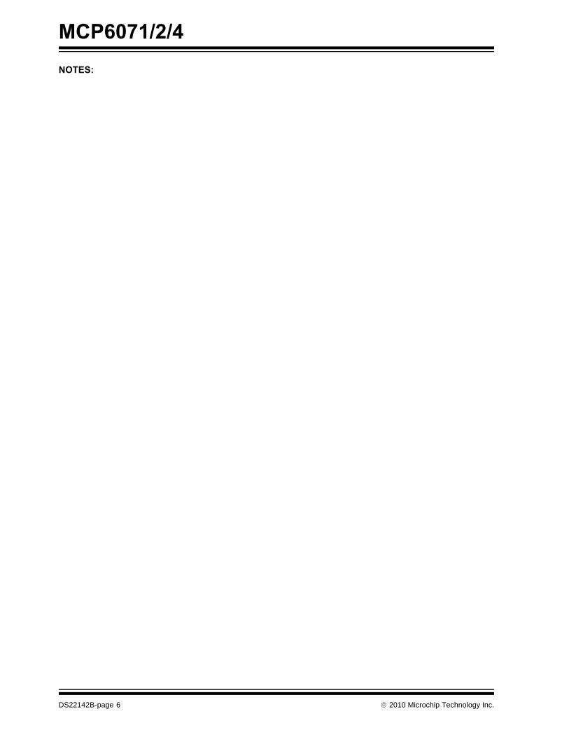
4.0 APPLICATION INFORMATIONThe MCP6071/2/4 family of op amps is manufacturedusing Microchip’s state-of-the-art CMOS process andis specifically designed for low-power, high precisionapplications.
4.1 Rail-to-Rail Input
4.1.1 PHASE REVERSALThe MCP6071/2/4 op amps are designed to preventphase reversal when the input pins exceed the supplyvoltages. Figure 2-34 shows the input voltageexceeding the supply voltage without any phasereversal.
4.1.2 INPUT VOLTAGE LIMITSIn order to prevent damage and/or improper operationof these amplifiers, the circuit must limit the voltages atthe input pins (see Section 1.1, Absolute MaximumRatings †).
The ESD protection on the inputs can be depicted asshown in Figure 4-1. This structure was chosen toprotect the input transistors and to minimize input biascurrent (IB).
FIGURE 4-1: Simplified Analog Input ESD Structures.The input ESD diodes clamp the inputs when they tryto go more than one diode drop below VSS. They alsoclamp any voltages that go well above VDD; their break-down voltage is high enough to allow normal operation,but not low enough to protect against slow over-voltage(beyond VDD) events. Very fast ESD events (that meetthe spec) are limited so that damage does not occur.
In some applications, it may be necessary to preventexcessive voltages from reaching the op amp inputs.Figure 4-2 shows one approach to protecting theseinputs.
FIGURE 4-2: Protecting the Analog Inputs.A significant amount of current can flow out of theinputs when the Common Mode voltage (VCM) is belowground (VSS). See Figure 2-36.
4.1.3 INPUT CURRENT LIMITSIn order to prevent damage and/or improper operationof these amplifiers, the circuit must limit the voltages atthe input pins (see Section 1.1, Absolute MaximumRatings †).
Figure 4-3 shows one approach to protecting theseinputs. The resistors R1 and R2 limit the possible cur-rents in or out of the input pins (and the ESD diodes, D1and D2). The diode currents will go through either VDDor VSS.
FIGURE 4-3: Protecting the Analog Inputs.
4.1.4 NORMAL OPERATIONThe input stage of the MCP6071/2/4 op amps use twodifferential input stages in parallel. One operates at alow common mode input voltage (VCM), while the otheroperates at a high VCM. With this topology, the deviceoperates with a VCM up to 300 mV above VDD and300 mV below VSS. (See Figure 2-13). The input offsetvoltage is measured at VCM = VSS – 0.3V andVDD + 0.3V to ensure proper operation.
The transition between the input stages occurs whenVCM is near VDD – 1.1V (See Figures 2-4, 2-5 andFigure 2-6). For the best distortion performance andgain linearity, with non-inverting gains, avoid this regionof operation.
BondPad
BondPad
BondPad
VDD
VIN+
VSS
InputStage
BondPad
VIN–
V1
VDD
D1
V2
D2
MCP607XVOUT
U1
V1R1
VDD
D1
min(R1,R2) >VSS – min (V1,V2)
2 mA
min(R1,R2) >max(V1,V2) – VDD
2 mA
V2R2
D2
MCP607XVOUT
U1
© 2010 Microchip Technology Inc. DS22142B-page 15
MCP6071/2/4
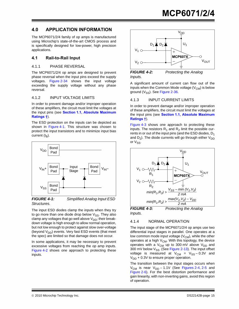
4.2 Rail-to-Rail OutputThe output voltage range of the MCP6071/2/4 op ampsis VSS + 15 mV (minimum) and VDD – 15 mV(maximum) when RL = 10 kΩ is connected to VDD/2and VDD = 6.0V. Refer to Figures 2-27 and 2-28 formore information.4.3 Capacitive LoadsDriving large capacitive loads can cause stabilityproblems for voltage feedback op amps. As the loadcapacitance increases, the feedback loop’s phasemargin decreases and the closed-loop bandwidth isreduced. This produces gain peaking in the frequencyresponse, with overshoot and ringing in the stepresponse. While a unity-gain buffer (G = +1) is the mostsensitive to capacitive loads, all gains show the samegeneral behavior.
When driving large capacitive loads with these opamps (e.g., > 100 pF when G = +1), a small seriesresistor at the output (RISO in Figure 4-4) improves thefeedback loop’s phase margin (stability) by making theoutput load resistive at higher frequencies. Thebandwidth will be generally lower than the bandwidthwith no capacitance load.
FIGURE 4-4: Output Resistor, RISO Stabilizes Large Capacitive Loads.Figure 4-5 gives recommended RISO values fordifferent capacitive loads and gains. The x-axis is thenormalized load capacitance (CL/GN), where GN is thecircuit's noise gain. For non-inverting gains, GN and theSignal Gain are equal. For inverting gains, GN is1+|Signal Gain| (e.g., -1 V/V gives GN = +2 V/V).
FIGURE 4-5: Recommended RISO Values for Capacitive Loads.
After selecting RISO for your circuit, double-check theresulting frequency response peaking and stepresponse overshoot. Modify RISO’s value until theresponse is reasonable. Bench evaluation andsimulations with the MCP6071/2/4 SPICE macromodel are very helpful.
4.4 Supply BypassWith this family of operational amplifiers, the powersupply pin (VDD for single-supply) should have a localbypass capacitor (i.e., 0.01 µF to 0.1 µF) within 2 mmfor good high frequency performance. It can use a bulkcapacitor (i.e., 1 µF or larger) within 100 mm to providelarge, slow currents. This bulk capacitor can be sharedwith other analog parts.
4.5 Unused Op AmpsAn unused op amp in a quad package (MCP6074)should be configured as shown in Figure 4-6. Thesecircuits prevent the output from toggling and causingcrosstalk. Circuit A sets the op amp at its minimumnoise gain. The resistor divider produces any desiredreference voltage within the output voltage range of theop amp; the op amp buffers that reference voltage.Circuit B uses the minimum number of componentsand operates as a comparator, but it may draw morecurrent.
FIGURE 4-6: Unused Op Amps.
VIN
RISOVOUTMCP607X
CL
–
+
1
10
100
1000
1.E-11 1.E-10 1.E-09 1.E-08 1.E-07 1.E-06Normalized Load Capacitance; CL/GN (F)
Rec
omm
ende
d R
ISO (Ω
)
GN: 1 V/V 2 V/V ≥ 5 V/V
VDD = 6.0 V RL = 10 kΩ
10p 100p 1n 10n 0.1µ 1µ
VDD
VDD
¼ MCP6074 (A) ¼ MCP6074 (B)
R1
R2
VDD
VREF
VREF VDDR2
R1 R2+--------------------×=
DS22142B-page 16 © 2010 Microchip Technology Inc.

MCP6071/2/4
4.6 PCB Surface LeakageIn applications where low input bias current is critical,Printed Circuit Board (PCB) surface leakage effectsneed to be considered. Surface leakage is caused byhumidity, dust or other contamination on the board.Under low humidity conditions, a typical resistancebetween nearby traces is 1012Ω. A 5V difference wouldcause 5 pA of current to flow; which is greater than theMCP6071/2/4 family’s bias current at +25°C (±1.0 pA,typical).The easiest way to reduce surface leakage is to use aguard ring around sensitive pins (or traces). The guardring is biased at the same voltage as the sensitive pin.An example of this type of layout is shown inFigure 4-7.
FIGURE 4-7: Example Guard Ring Layout for Inverting Gain.1. Non-inverting Gain and Unity-Gain Buffer:
a.Connect the non-inverting pin (VIN+) to theinput with a wire that does not touch thePCB surface.
b.Connect the guard ring to the inverting inputpin (VIN–). This biases the guard ring to thecommon mode input voltage.
2. Inverting Gain and Transimpedance GainAmplifiers (convert current to voltage, such asphoto detectors):a.Connect the guard ring to the non-inverting
input pin (VIN+). This biases the guard ringto the same reference voltage as the opamp (e.g., VDD/2 or ground).
b.Connect the inverting pin (VIN–) to the inputwith a wire that does not touch the PCBsurface.
Guard Ring VIN– VIN+ VSS
© 2010 Microchip Technology Inc. DS22142B-page 17

MCP6071/2/4
4.7 Application Circuits4.7.1 GYRATOR
The MCP6071/2/4 op amps can be used in gyratorapplications. The gyrator is an electric circuit which canmake a capacitive circuit behave inductively.
Figure 4-8 shows an example of a gyrator simulatinginductance, with an approximately equivalent circuitbelow. The two ZIN have similar values in typicalapplications. The primary application for a gyrator is toreduce the size and cost of a system by removing theneed for bulky, heavy and expensive inductors. Forexample, RLC bandpass filter characteristics can berealized with capacitors, resistors and operationalamplifiers without using inductors. Moreover, gyratorswill typically have higher accuracy than real inductors,due to the lower cost of precision capacitors thaninductors..
FIGURE 4-8: Gyrator.
4.7.2 INSTRUMENTATION AMPLIFIERThe MCP6071/2/4 op amps are well suited forconditioning sensor signals in battery-poweredapplications. Figure 4-9 shows a two op ampinstrumentation amplifier, using the MCP6072, thatworks well for applications requiring rejection ofcommon mode noise at higher gains. The referencevoltage (VREF) is supplied by a low impedance source.In single supply applications, VREF is typically VDD/2.
FIGURE 4-9: Two Op Amp Instrumentation Amplifier.To obtain the best CMRR possible, and not limit theperformance by the resistor tolerances, set a high gainwith the RG resistor.
4.7.3 PRECISION COMPARATORUse high gain before a comparator to improve thelatter’s input offset performance. Figure 4-10 shows again of 11 V/V placed before a comparator. Thereference voltage VREF can be any value between thesupply rails.
FIGURE 4-10: Precision, Non-inverting Comparator.
MCP6071
RL
VOUT
Gyrator
ZIN
R
C
ZIN RL jωL+=
L RLRC=
RL
L
ZIN
Equivalent Circuit
VOUT V1 V2–( ) 1R1R2------
2R1RG---------+ +⎝ ⎠
⎛ ⎞ VREF+=
VREF R1 R2 R2 R1 VOUT
RG
V2
V1
½MCP6072
½MCP6072
VIN
1 MΩ VOUT
MCP6071
100 kΩMCP6541
VREF
DS22142B-page 18 © 2010 Microchip Technology Inc.

MCP6071/2/4
5.0 DESIGN AIDSMicrochip provides the basic design tools needed forthe MCP6071/2/4 family of op amps.
5.1 SPICE Macro ModelThe latest SPICE macro model for the MCP6071/2/4op amps is available on the Microchip web site atwww.microchip.com. The model was written and testedin official Orcad (Cadence) owned PSPICE. For theother simulators, it may require translation.
The model covers a wide aspect of the op amp'selectrical specifications. Not only does the model covervoltage, current, and resistance of the op amp, but italso covers the temperature and noise effects on thebehavior of the op amp. The model has not beenverified outside of the specification range listed in theop amp data sheet. The model behaviors under theseconditions can not be guaranteed that it will match theactual op amp performance.
Moreover, the model is intended to be an initial designtool. Bench testing is a very important part of anydesign and cannot be replaced with simulations. Also,simulation results using this macro model need to bevalidated by comparing them to the data sheetspecifications and characteristic curves.
5.2 FilterLab® SoftwareMicrochip’s FilterLab® software is an innovativesoftware tool that simplifies analog active filter (usingop amps) design. Available at no cost from theMicrochip web site at www.microchip.com/filterlab, theFilterLab design tool provides full schematic diagramsof the filter circuit with component values. It alsooutputs the filter circuit in SPICE format, which can beused with the macro model to simulate actual filterperformance.
5.3 MAPS (Microchip Advanced Part Selector)
MAPS is a software tool that helps semiconductorprofessionals efficiently identify Microchip devices thatfit a particular design requirement. Available at no costfrom the Microchip website at www.microchip.com/maps, the MAPS is an overall selection tool forMicrochip’s product portfolio that includes Analog,Memory, MCUs and DSCs. Using this tool you candefine a filter to sort features for a parametric search ofdevices and export side-by-side technical comparisonreports. Helpful links are also provided for Data Sheets,purchase, and sampling of Microchip parts.
5.4 Analog Demonstration and Evaluation Boards
Microchip offers a broad spectrum of AnalogDemonstration and Evaluation Boards that aredesigned to help you achieve faster time to market. Fora complete listing of these boards and theircorresponding user’s guides and technical information,visit the Microchip web site at www.microchip.com/analogtools.
Some boards that are especially useful are:
• MCP6XXX Amplifier Evaluation Board 1• MCP6XXX Amplifier Evaluation Board 2• MCP6XXX Amplifier Evaluation Board 3• MCP6XXX Amplifier Evaluation Board 4• Active Filter Demo Board Kit• 5/6-Pin SOT-23 Evaluation Board, P/N VSUPEV2• 8-Pin SOIC/MSOP/TSSOP/DIP Evaluation Board,
P/N SOIC8EV• 14-Pin SOIC/TSSOP/DIP Evaluation Board, P/N
SOIC14EV
5.5 Application NotesThe following Microchip Analog Design Note andApplication Notes are available on the Microchip website at www.microchip. com/appnotes and arerecommended as supplemental reference resources.
• ADN003: “Select the Right Operational Amplifier for your Filtering Circuits”, DS21821
• AN722: “Operational Amplifier Topologies and DC Specifications”, DS00722
• AN723: “Operational Amplifier AC Specifications and Applications”, DS00723
• AN884: “Driving Capacitive Loads With Op Amps”, DS00884
• AN990: “Analog Sensor Conditioning Circuits –An Overview”, DS00990
• AN1177: “Op Amp Precision Design: DC Errors”, DS01177
• AN1228: “Op Amp Precision Design: Random Noise”, DS01228
• AN1332: “Current Sensing Circuit Concepts and Fundamentals”, DS01332
These application notes and others are listed in thedesign guide:
• “Signal Chain Design Guide”, DS21825
© 2010 Microchip Technology Inc. DS22142B-page 19

MCP6071/2/4
NOTES:DS22142B-page 20 © 2010 Microchip Technology Inc.

MCP6071/2/4
6.0 PACKAGING INFORMATION
6.1 Package Marking Information
Legend: XX...X Customer-specific informationY Year code (last digit of calendar year)YY Year code (last 2 digits of calendar year)WW Week code (week of January 1 is week ‘01’)NNN Alphanumeric traceability code Pb-free JEDEC designator for Matte Tin (Sn)* This package is Pb-free. The Pb-free JEDEC designator ( )
can be found on the outer packaging for this package.
Note: In the event the full Microchip part number cannot be marked on one line, it willbe carried over to the next line, thus limiting the number of availablecharacters for customer-specific information.
3e
3e
8-Lead SOIC (150 mil) (MCP6071, MCP6072) Example:
XXXXXXXXXXXXYYWW
NNN
MCP6071ESN^^ 1044
2563e
Example:
AHE04425
8-Lead 2x3 TDFN (MCP6071, MCP6072)
XXXYWWNN
5-Lead SOT-23 (MCP6071)
XXNN
Example:
YH25
© 2010 Microchip Technology Inc. DS22142B-page 21

MCP6071/2/4
Package Marking Information (Continuation)14-Lead TSSOP (MCP6074) Example:
14-Lead SOIC (150 mil) (MCP6074) Example:
XXXXXXXXXXX
YYWWNNN
XXXXXXXXYYWW
NNN
MCP6074E1044
256
XXXXXXXXXXXMCP6074
1044256E/SL 3e
DS22142B-page 22 © 2010 Microchip Technology Inc.

MCP6071/2/4
!"!#$! !% #$ !% #$ # & ! ! !# "'(
)*+ ) # &#,$ --#$##
.# #$ #/ !- 0 # 1/ %## !###+22---2/
3# 44"" 4# 5 56 7
5$8 %1 5 (4 !1# ()*6$# ! 4 !1# )*6, 9 # : (! !1/ / ; : #!%% : (6, <!# " : ! !1/ <!# " : ;6, 4 # : .#4 # 4 : =.## 4 ( : ;.# > : >4 !/ ; : =4 !<!# 8 : (
φ
Nb
E
E1
D
1 2 3
e
e1
A
A1
A2 c
L
L1
- *)
© 2010 Microchip Technology Inc. DS22142B-page 23

MCP6071/2/4
Note: For the most current package drawings, please see the Microchip Packaging Specification located at http://www.microchip.com/packaging
DS22142B-page 24 © 2010 Microchip Technology Inc.

MCP6071/2/4
Note: For the most current package drawings, please see the Microchip Packaging Specification located at http://www.microchip.com/packaging
© 2010 Microchip Technology Inc. DS22142B-page 25

MCP6071/2/4
Note: For the most current package drawings, please see the Microchip Packaging Specification located at http://www.microchip.com/packaging
DS22142B-page 26 © 2010 Microchip Technology Inc.

MCP6071/2/4
Note: For the most current package drawings, please see the Microchip Packaging Specification located at http://www.microchip.com/packaging
© 2010 Microchip Technology Inc. DS22142B-page 27

MCP6071/2/4
Note: For the most current package drawings, please see the Microchip Packaging Specification located at http://www.microchip.com/packaging
DS22142B-page 28 © 2010 Microchip Technology Inc.

MCP6071/2/4
!"#$%&''()*+, !
.# #$ #/ !- 0 # 1/ %## !###+22---2/
© 2010 Microchip Technology Inc. DS22142B-page 29

MCP6071/2/4
-. &/")0(+,12
1, $! &% #$ ,08$#$ #8 # !-## # ! R%#*# # !"!#$! !% #$ !% #$ # & !( ! !# "'(
)*+ ) # &#,$ --#$## ".+ % 0$ $-#$## 0%%#$
.# #$ #/ !- 0 # 1/ %## !###+22---2/
3# 44"" 4# 5 56 7
5$8 %1 5 1# )*6, 9 # : : (! !1/ / ( : :#!%%R : (6, <!# " =)*! !1/ <!# " )*6, 4 # ;=()**% U#V ( : (.#4 # 4 : .## 4 "..# > : ;>4 !/ : (4 !<!# 8 : (!%# (> : (>!%# )## (> : (>
NOTE 1
N
D
E
E1
1 2 3
b
e
A
A1
A2
L
L1
c
h
h α
β
φ
- *=()
DS22142B-page 30 © 2010 Microchip Technology Inc.

MCP6071/2/4
.# #$ #/ !- 0 # 1/ %## !###+22---2/
© 2010 Microchip Technology Inc. DS22142B-page 31

MCP6071/2/4
Note: For the most current package drawings, please see the Microchip Packaging Specification located at http://www.microchip.com/packaging
DS22142B-page 32 © 2010 Microchip Technology Inc.

MCP6071/2/4
Note: For the most current package drawings, please see the Microchip Packaging Specification located at http://www.microchip.com/packaging
© 2010 Microchip Technology Inc. DS22142B-page 33

MCP6071/2/4
Note: For the most current package drawings, please see the Microchip Packaging Specification located at http://www.microchip.com/packaging
DS22142B-page 34 © 2010 Microchip Technology Inc.

MCP6071/2/4
APPENDIX A: REVISION HISTORY
Revision B (December 2010)The following is the list of modifications:
1. Added new SOT-23-5 package type forMCP6071 device.
2. Corrected Figures 2-13, 2-22, 2-23, 2-24, 2-28,2-29 and 2-34 in Section 2.0 “Typical
Performance Curves”.3. Modified Table 3-1 to show the pin column for
MCP6071, SOT-23-5 package.4. Updated Section 4.1.2 “Input Voltage Limits”.5. Added Section 4.1.3 “Input Current Limits”.6. Added new document item in Section 5.5
“Application Notes”.7. Updated the Product Identification System
page.
Revision A (March 2009)• Original Release of this Document.
© 2010 Microchip Technology Inc. DS22142B-page 35

MCP6071/2/4
NOTES:DS22142B-page 36 © 2010 Microchip Technology Inc.

MCP6071/2/4
PRODUCT IDENTIFICATION SYSTEMTo order or obtain information, e.g., on pricing or delivery, refer to the factory or the listed sales office.
Device: MCP6071: Single Op AmpMCP6071T: Single Op Amp (Tape and Reel)
(SOIC, SOT-23 and 2x3 TDFN)MCP6072: Dual Op AmpMCP6072T: Dual Op Amp (Tape and Reel)
(SOIC and 2x3 TDFN)MCP6074: Quad Op AmpMCP6074T: Quad Op Amp (Tape and Reel)
(SOIC and TSSOP)
Temperature Range: E = -40°C to +125°C
Package: MNY * = Plastic Dual Flat, No Lead, (2x3 TDFN ) 8-leaddOT = Plastic Small Outline Transistor (SOT-23), 5-leadSL = Plastic SOIC (150 mil Body), 14-leadSN = Plastic SOIC, (150 mil Body), 8-leadST = Plastic TSSOP (4.4mm Body), 14-lead
* Y = Nickel palladium gold manufacturing designator. Only available on the TDFN package.
PART NO. -X /XX
PackageTemperatureRange
Device
Examples:
a) MCP6071T-E/OT: Tape and Reel,5LD SOT-23 pkg
b) MCP6071-E/SN: 8LD SOIC pkgc) MCP6071T-E/SN: Tape and Reel,
8LD SOIC pkgd) MCP6071T-E/MNY: Tape and Reel,
8LD 2x3 TDFN pkg
a) MCP6072-E/SN: 8LD SOIC pkgb) MCP6072T-E/SN: Tape and Reel,
8LD SOIC pkgc) MCP6072T-E/MNY: Tape and Reel
8LD 2x3 TDFN pkg
a) MCP6074-E/SL: 14LD SOIC pkgb) MCP6074T-E/SL: Tape and Reel,
14LD SOIC pkgc) MCP6074-E/ST: 14LD TSSOP pkgd) MCP6074T-E/ST: Tape and Reel,
14LD TSSOP pkg
© 2010 Microchip Technology Inc. DS22142B-page 37

MCP6071/2/4
NOTES:DS22142B-page 38 © 2010 Microchip Technology Inc.

Note the following details of the code protection feature on Microchip devices:• Microchip products meet the specification contained in their particular Microchip Data Sheet.
• Microchip believes that its family of products is one of the most secure families of its kind on the market today, when used in the intended manner and under normal conditions.
• There are dishonest and possibly illegal methods used to breach the code protection feature. All of these methods, to our knowledge, require using the Microchip products in a manner outside the operating specifications contained in Microchip’s Data Sheets. Most likely, the person doing so is engaged in theft of intellectual property.
• Microchip is willing to work with the customer who is concerned about the integrity of their code.
• Neither Microchip nor any other semiconductor manufacturer can guarantee the security of their code. Code protection does not mean that we are guaranteeing the product as “unbreakable.”
Code protection is constantly evolving. We at Microchip are committed to continuously improving the code protection features of ourproducts. Attempts to break Microchip’s code protection feature may be a violation of the Digital Millennium Copyright Act. If such actsallow unauthorized access to your software or other copyrighted work, you may have a right to sue for relief under that Act.
Information contained in this publication regarding deviceapplications and the like is provided only for your convenienceand may be superseded by updates. It is your responsibility toensure that your application meets with your specifications.MICROCHIP MAKES NO REPRESENTATIONS ORWARRANTIES OF ANY KIND WHETHER EXPRESS ORIMPLIED, WRITTEN OR ORAL, STATUTORY OROTHERWISE, RELATED TO THE INFORMATION,INCLUDING BUT NOT LIMITED TO ITS CONDITION,QUALITY, PERFORMANCE, MERCHANTABILITY ORFITNESS FOR PURPOSE. Microchip disclaims all liabilityarising from this information and its use. Use of Microchipdevices in life support and/or safety applications is entirely atthe buyer’s risk, and the buyer agrees to defend, indemnify andhold harmless Microchip from any and all damages, claims,suits, or expenses resulting from such use. No licenses areconveyed, implicitly or otherwise, under any Microchipintellectual property rights.
© 2010 Microchip Technology Inc.
Trademarks
The Microchip name and logo, the Microchip logo, dsPIC, KEELOQ, KEELOQ logo, MPLAB, PIC, PICmicro, PICSTART, PIC32 logo, rfPIC and UNI/O are registered trademarks of Microchip Technology Incorporated in the U.S.A. and other countries.
FilterLab, Hampshire, HI-TECH C, Linear Active Thermistor, MXDEV, MXLAB, SEEVAL and The Embedded Control Solutions Company are registered trademarks of Microchip Technology Incorporated in the U.S.A.
Analog-for-the-Digital Age, Application Maestro, CodeGuard, dsPICDEM, dsPICDEM.net, dsPICworks, dsSPEAK, ECAN, ECONOMONITOR, FanSense, HI-TIDE, In-Circuit Serial Programming, ICSP, Mindi, MiWi, MPASM, MPLAB Certified logo, MPLIB, MPLINK, mTouch, Omniscient Code Generation, PICC, PICC-18, PICDEM, PICDEM.net, PICkit, PICtail, REAL ICE, rfLAB, Select Mode, Total Endurance, TSHARC, UniWinDriver, WiperLock and ZENA are trademarks of Microchip Technology Incorporated in the U.S.A. and other countries.
SQTP is a service mark of Microchip Technology Incorporated in the U.S.A.
All other trademarks mentioned herein are property of their respective companies.
© 2010, Microchip Technology Incorporated, Printed in the U.S.A., All Rights Reserved.
Printed on recycled paper.
ISBN: 978-1-60932-732-3
DS22142B-page 39
Microchip received ISO/TS-16949:2002 certification for its worldwide headquarters, design and wafer fabrication facilities in Chandler and Tempe, Arizona; Gresham, Oregon and design centers in California and India. The Company’s quality system processes and procedures are for its PIC® MCUs and dsPIC® DSCs, KEELOQ® code hopping devices, Serial EEPROMs, microperipherals, nonvolatile memory and analog products. In addition, Microchip’s quality system for the design and manufacture of development systems is ISO 9001:2000 certified.

DS22142B-page 40 © 2010 Microchip Technology Inc.
AMERICASCorporate Office2355 West Chandler Blvd.Chandler, AZ 85224-6199Tel: 480-792-7200 Fax: 480-792-7277Technical Support: http://support.microchip.comWeb Address: www.microchip.comAtlantaDuluth, GA Tel: 678-957-9614 Fax: 678-957-1455BostonWestborough, MA Tel: 774-760-0087 Fax: 774-760-0088ChicagoItasca, IL Tel: 630-285-0071 Fax: 630-285-0075ClevelandIndependence, OH Tel: 216-447-0464 Fax: 216-447-0643DallasAddison, TX Tel: 972-818-7423 Fax: 972-818-2924DetroitFarmington Hills, MI Tel: 248-538-2250Fax: 248-538-2260KokomoKokomo, IN Tel: 765-864-8360Fax: 765-864-8387Los AngelesMission Viejo, CA Tel: 949-462-9523 Fax: 949-462-9608Santa ClaraSanta Clara, CA Tel: 408-961-6444Fax: 408-961-6445TorontoMississauga, Ontario, CanadaTel: 905-673-0699 Fax: 905-673-6509
ASIA/PACIFICAsia Pacific OfficeSuites 3707-14, 37th FloorTower 6, The GatewayHarbour City, KowloonHong KongTel: 852-2401-1200Fax: 852-2401-3431Australia - SydneyTel: 61-2-9868-6733Fax: 61-2-9868-6755China - BeijingTel: 86-10-8528-2100 Fax: 86-10-8528-2104China - ChengduTel: 86-28-8665-5511Fax: 86-28-8665-7889China - ChongqingTel: 86-23-8980-9588Fax: 86-23-8980-9500China - Hong Kong SARTel: 852-2401-1200 Fax: 852-2401-3431China - NanjingTel: 86-25-8473-2460Fax: 86-25-8473-2470China - QingdaoTel: 86-532-8502-7355Fax: 86-532-8502-7205China - ShanghaiTel: 86-21-5407-5533 Fax: 86-21-5407-5066China - ShenyangTel: 86-24-2334-2829Fax: 86-24-2334-2393China - ShenzhenTel: 86-755-8203-2660 Fax: 86-755-8203-1760China - WuhanTel: 86-27-5980-5300Fax: 86-27-5980-5118China - XianTel: 86-29-8833-7252Fax: 86-29-8833-7256China - XiamenTel: 86-592-2388138 Fax: 86-592-2388130China - ZhuhaiTel: 86-756-3210040 Fax: 86-756-3210049
ASIA/PACIFICIndia - BangaloreTel: 91-80-3090-4444 Fax: 91-80-3090-4123India - New DelhiTel: 91-11-4160-8631Fax: 91-11-4160-8632India - PuneTel: 91-20-2566-1512Fax: 91-20-2566-1513Japan - YokohamaTel: 81-45-471- 6166 Fax: 81-45-471-6122Korea - DaeguTel: 82-53-744-4301Fax: 82-53-744-4302Korea - SeoulTel: 82-2-554-7200Fax: 82-2-558-5932 or 82-2-558-5934Malaysia - Kuala LumpurTel: 60-3-6201-9857Fax: 60-3-6201-9859Malaysia - PenangTel: 60-4-227-8870Fax: 60-4-227-4068Philippines - ManilaTel: 63-2-634-9065Fax: 63-2-634-9069SingaporeTel: 65-6334-8870Fax: 65-6334-8850Taiwan - Hsin ChuTel: 886-3-6578-300Fax: 886-3-6578-370Taiwan - KaohsiungTel: 886-7-213-7830Fax: 886-7-330-9305Taiwan - TaipeiTel: 886-2-2500-6610 Fax: 886-2-2508-0102Thailand - BangkokTel: 66-2-694-1351Fax: 66-2-694-1350
EUROPEAustria - WelsTel: 43-7242-2244-39Fax: 43-7242-2244-393Denmark - CopenhagenTel: 45-4450-2828 Fax: 45-4485-2829France - ParisTel: 33-1-69-53-63-20 Fax: 33-1-69-30-90-79Germany - MunichTel: 49-89-627-144-0 Fax: 49-89-627-144-44Italy - Milan Tel: 39-0331-742611 Fax: 39-0331-466781Netherlands - DrunenTel: 31-416-690399 Fax: 31-416-690340Spain - MadridTel: 34-91-708-08-90Fax: 34-91-708-08-91UK - WokinghamTel: 44-118-921-5869Fax: 44-118-921-5820
Worldwide Sales and Service
08/04/10