10.7 - MEDIUM SPEED ANALOG-DIGITAL...
24
CMOS Analog IC Design Page 10.7-1 Chapter 10 - DA and AD Converters (6/4/01) © P.E. Allen, 2001 10.7 - MEDIUM SPEED ANALOG-DIGITAL CONVERTERS INTRODUCTION Successive Approximation Algorithm: 1.) Start with the MSB bit and work toward the LSB bit. 2.) Guess the MSB bit as 1. 3.) Apply the digital word 10000.... to a DAC. 4.) Compare the DAC output with the sampled analog input voltage. 5.) If the DAC output is greater, keep the guess of 1. If the DAC output is less, change the guess to 0. 6.) Repeat for the next MSB. If the number of bits is N, the time for conversion will be NT where T is the clock period. Illustration:
Transcript of 10.7 - MEDIUM SPEED ANALOG-DIGITAL...
CMOS Analog IC Design Page 10.7-1
Chapter 10 - DA and AD Converters (6/4/01) © P.E. Allen, 2001
10.7 - MEDIUM SPEED ANALOG-DIGITAL CONVERTERS INTRODUCTION
Successive Approximation Algorithm:
1.) Start with the MSB bit and work toward the LSB bit.
2.) Guess the MSB bit as 1.
3.) Apply the digital word 10000.... to a DAC.
4.) Compare the DAC output with the sampled analog input voltage.
5.) If the DAC output is greater, keep the guess of 1. If the DAC output is less, change the guess to 0.
6.) Repeat for the next MSB.
If the number of bits is N, the time for conversion will be NT where T is the clock period.
Illustration:
CMOS Analog IC Design Page 10.7-2
Chapter 10 - DA and AD Converters (6/4/01) © P.E. Allen, 2001
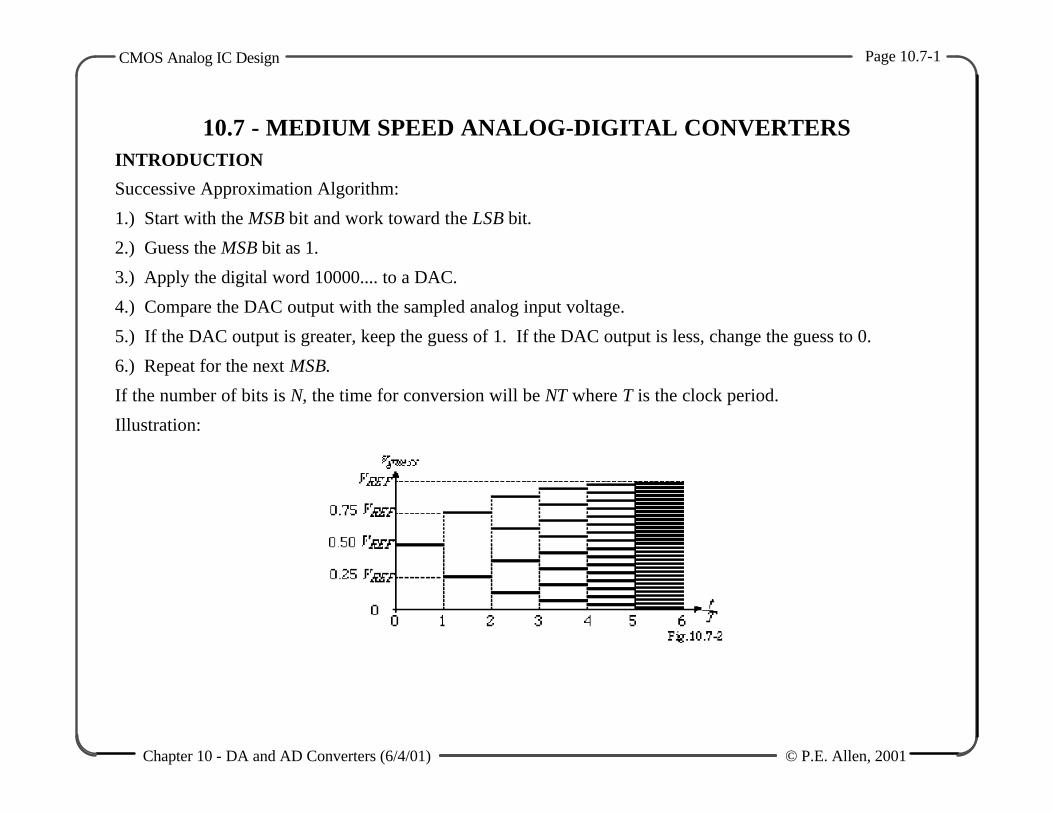
BLOCK DIAGRAM OF A SUCCESSIVE APPROXIMATION ADC†
† R. Hnatek, A User's Handbook of D/A and A/D Converters, JohnWiley and Sons, Inc., New York, NY, 1976.
CMOS Analog IC Design Page 10.7-3
Chapter 10 - DA and AD Converters (6/4/01) © P.E. Allen, 2001
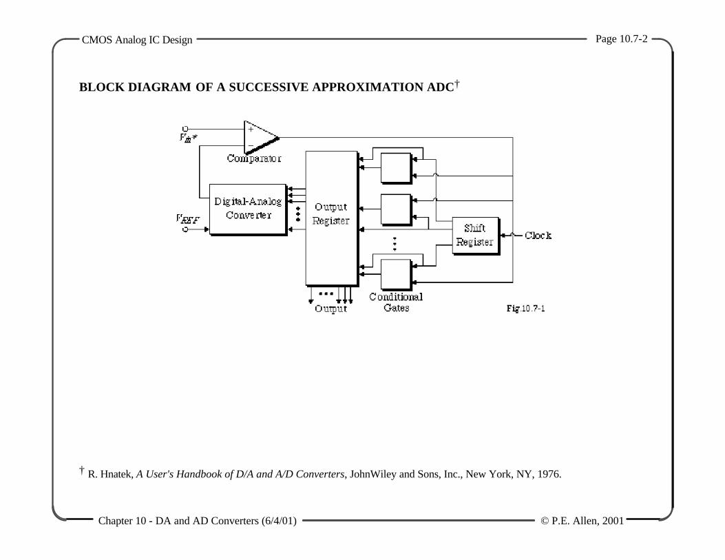
5-BIT SUCCESSIVE APPROXIMATION ADC
CMOS Analog IC Design Page 10.7-4
Chapter 10 - DA and AD Converters (6/4/01) © P.E. Allen, 2001
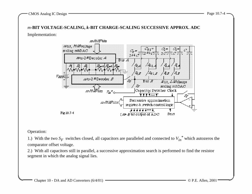
m-BIT VOLTAGE-SCALING, k-BIT CHARGE-SCALING SUCCESSIVE APPROX. ADC
Implementation:
Operation:
1.) With the two SF switches closed, all capacitors are paralleled and connected to Vin* which autozeros the
comparator offset voltage. 2.) With all capacitors still in parallel, a successive approximation search is performed to find the resistor segment in which the analog signal lies.
CMOS Analog IC Design Page 10.7-5
Chapter 10 - DA and AD Converters (6/4/01) © P.E. Allen, 2001
3.) Finally, a successive approximation search is performed on charge scaling subDAC to establish the analog output voltage.
CMOS Analog IC Design Page 10.7-6
Chapter 10 - DA and AD Converters (6/4/01) © P.E. Allen, 2001
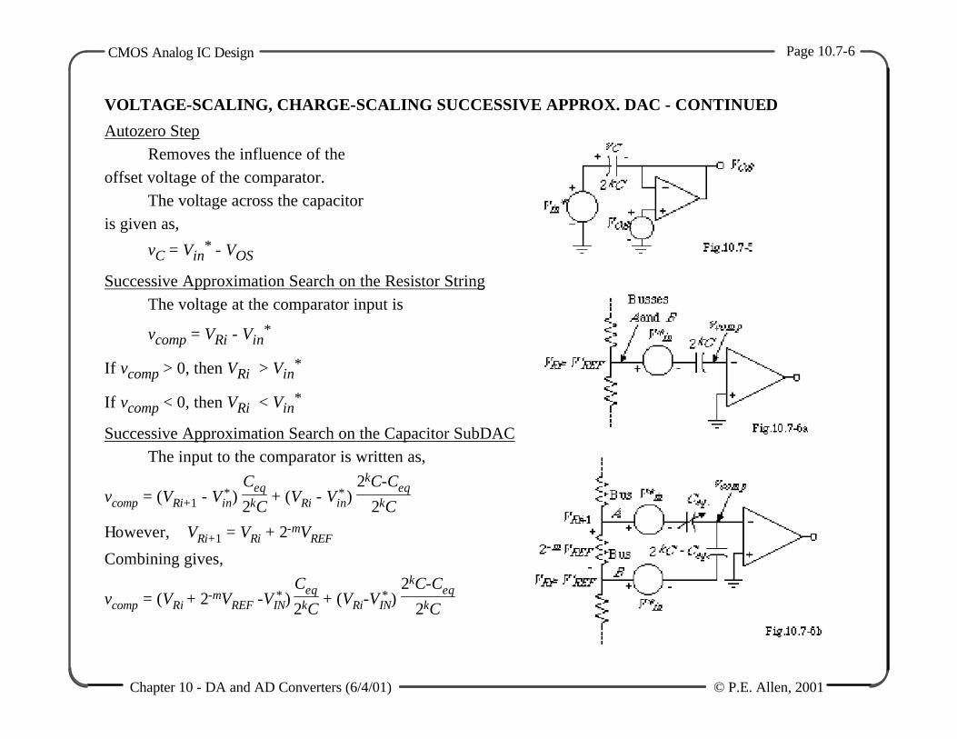
VOLTAGE-SCALING, CHARGE-SCALING SUCCESSIVE APPROX. DAC - CONTINUED
Autozero Step Removes the influence of the offset voltage of the comparator. The voltage across the capacitor is given as,
vC = Vin* - VOS
Successive Approximation Search on the Resistor String The voltage at the comparator input is
vcomp = VRi - Vin*
If vcomp > 0, then VRi > Vin*
If vcomp < 0, then VRi < Vin*
Successive Approximation Search on the Capacitor SubDAC The input to the comparator is written as,
vcomp = (VRi+1 - V*in)
Ceq
2kC + (VRi - V
*in)
2kC-Ceq
2kC
However, VRi+1 = VRi + 2-mVREF
Combining gives,
vcomp = (VRi + 2-mVREF -V *IN)
Ceq
2kC + (VRi-V
*IN)
2kC-Ceq
2kC
CMOS Analog IC Design Page 10.7-7
Chapter 10 - DA and AD Converters (6/4/01) © P.E. Allen, 2001
= VRi - V*IN + 2-mVREF
Ceq
2kC
CMOS Analog IC Design Page 10.7-8
Chapter 10 - DA and AD Converters (6/4/01) © P.E. Allen, 2001
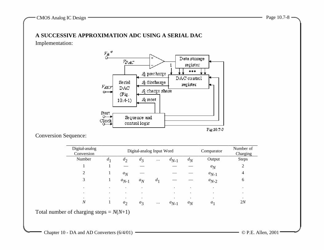
A SUCCESSIVE APPROXIMATION ADC USING A SERIAL DAC Implementation:
Conversion Sequence:
Digital-analog Conversion
Digital-analog Input Word Comparator Number of Charging
Number d1 d2 d3 ... dN-1 dN Output Steps
1 1 — — — — aN 2
2 1 aN — — — aN-1 4
3 1 aN-1 aN d1 — — aN-2 6
. . . . . . . .
. . . . . . . .
. . . . . . . . N 1 a2 a3 ... aN-1 aN a1 2N
Total number of charging steps = N(N+1)
CMOS Analog IC Design Page 10.7-9
Chapter 10 - DA and AD Converters (6/4/01) © P.E. Allen, 2001
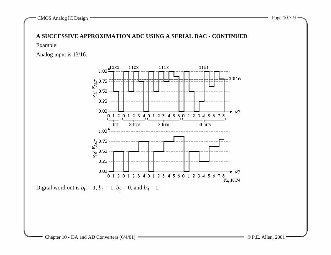
A SUCCESSIVE APPROXIMATION ADC USING A SERIAL DAC - CONTINUED
Example:
Analog input is 13/16.
Digital word out is b0 = 1, b1 = 1, b2 = 0, and b3 = 1.
CMOS Analog IC Design Page 10.7-10
Chapter 10 - DA and AD Converters (6/4/01) © P.E. Allen, 2001
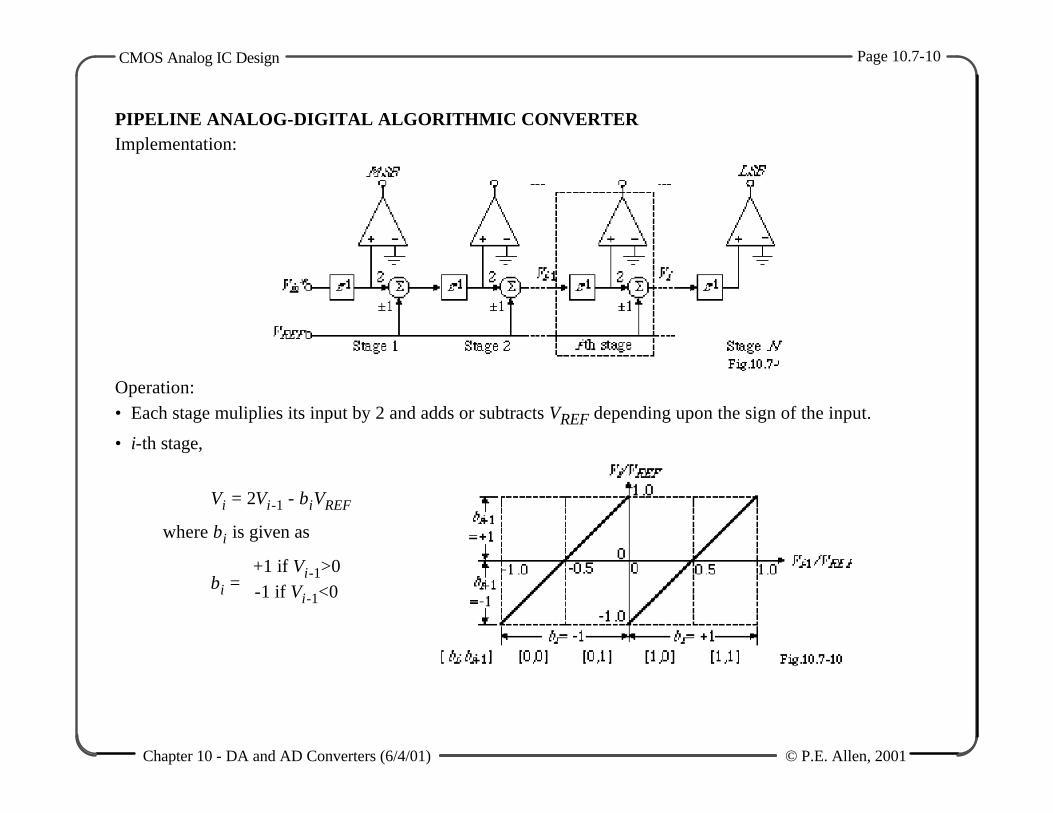
PIPELINE ANALOG-DIGITAL ALGORITHMIC CONVERTER Implementation:
Operation: • Each stage muliplies its input by 2 and adds or subtracts VREF depending upon the sign of the input.
• i-th stage,
Vi = 2Vi-1 - biVREF
where bi is given as
bi = +1 if Vi-1>0
-1 if Vi-1<0
CMOS Analog IC Design Page 10.7-11
Chapter 10 - DA and AD Converters (6/4/01) © P.E. Allen, 2001
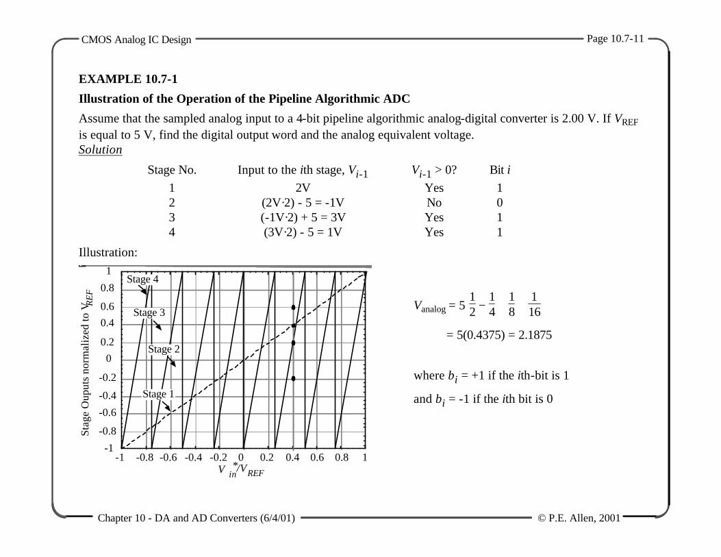
EXAMPLE 10.7-1
Illustration of the Operation of the Pipeline Algorithmic ADC
Assume that the sampled analog input to a 4-bit pipeline algorithmic analog-digital converter is 2.00 V. If VREF is equal to 5 V, find the digital output word and the analog equivalent voltage. Solution
Stage No. Input to the ith stage, Vi-1 Vi-1 > 0? Bit i 1 2V Yes 1 2 (2V·2) - 5 = -1V No 0 3 (-1V·2) + 5 = 3V Yes 1 4 (3V·2) - 5 = 1V Yes 1
Illustration:
Vanalog = 5
1
2 − 14 +
18 +
116
= 5(0.4375) = 2.1875
where bi = +1 if the ith-bit is 1
and bi = -1 if the ith bit is 0
-1
-0.8
-0.6
-0.4
-0.2
00.2
Stag
e O
uput
s no
rmal
ized
to V
0.40.6
0.8
1
-1 -0.8 -0.6 -0.4 -0.2 0 0.2 0.4 0.6 0.8 1
REF
Stage 1
Stage 2
Stage 3
Stage 4
V in*/VREF
CMOS Analog IC Design Page 10.7-12
Chapter 10 - DA and AD Converters (6/4/01) © P.E. Allen, 2001
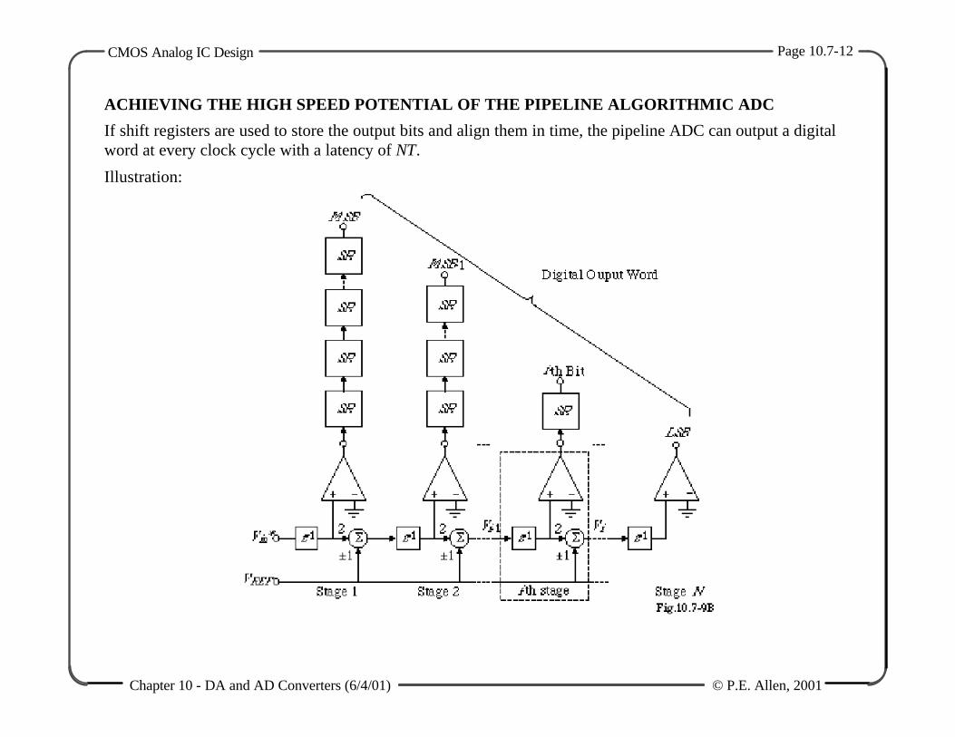
ACHIEVING THE HIGH SPEED POTENTIAL OF THE PIPELINE ALGORITHMIC ADC
If shift registers are used to store the output bits and align them in time, the pipeline ADC can output a digital word at every clock cycle with a latency of NT.
Illustration:
CMOS Analog IC Design Page 10.7-13
Chapter 10 - DA and AD Converters (6/4/01) © P.E. Allen, 2001
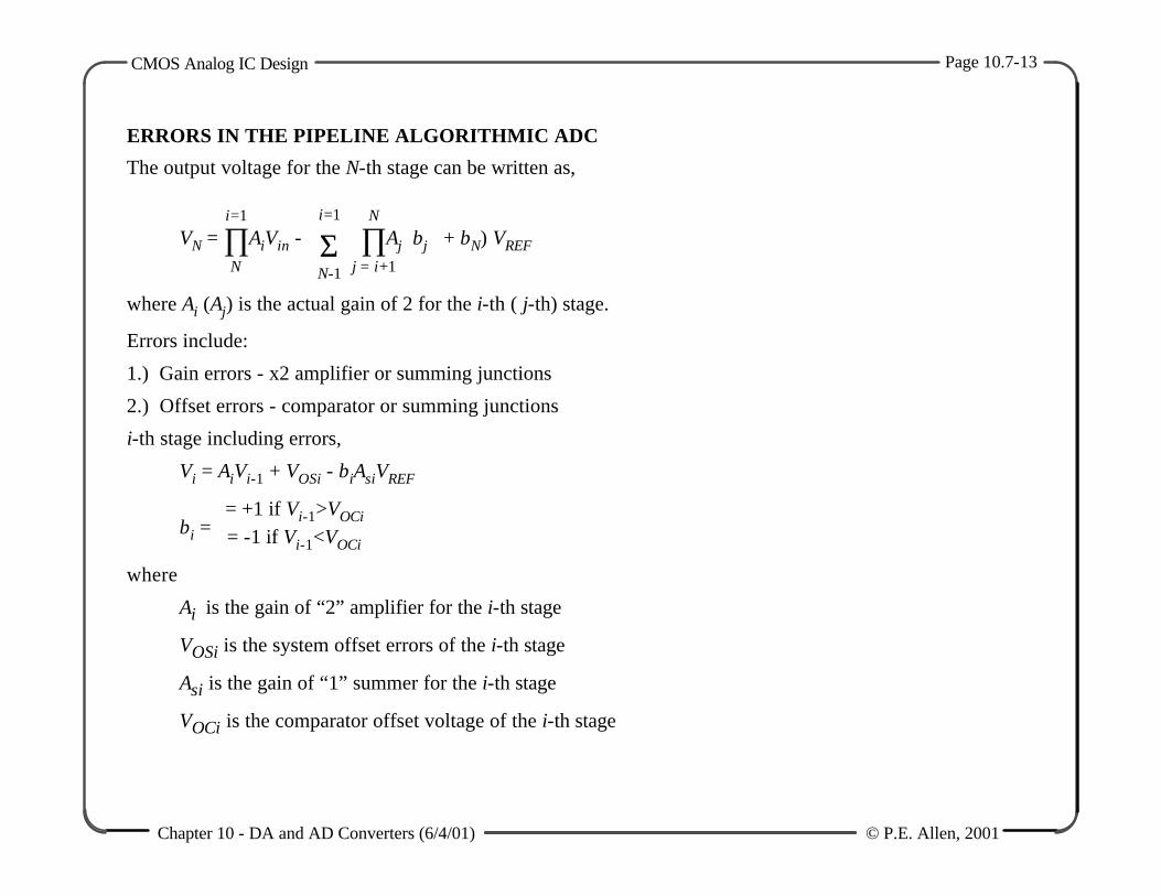
ERRORS IN THE PIPELINE ALGORITHMIC ADC
The output voltage for the N-th stage can be written as,
VN = ∏N
i=1AiVin -
i=1
ΣN-1
∏
j = i+1
NAj bj + bN) VREF
where Ai (Aj) is the actual gain of 2 for the i-th ( j-th) stage.
Errors include:
1.) Gain errors - x2 amplifier or summing junctions
2.) Offset errors - comparator or summing junctions
i-th stage including errors,
Vi = AiVi-1 + VOSi - biAsiVREF
bi = = +1 if Vi-1>VOCi
= -1 if Vi-1<VOCi
where
Ai is the gain of “2” amplifier for the i-th stage
VOSi is the system offset errors of the i-th stage
Asi is the gain of “1” summer for the i-th stage
VOCi is the comparator offset voltage of the i-th stage
CMOS Analog IC Design Page 10.7-14
Chapter 10 - DA and AD Converters (6/4/01) © P.E. Allen, 2001
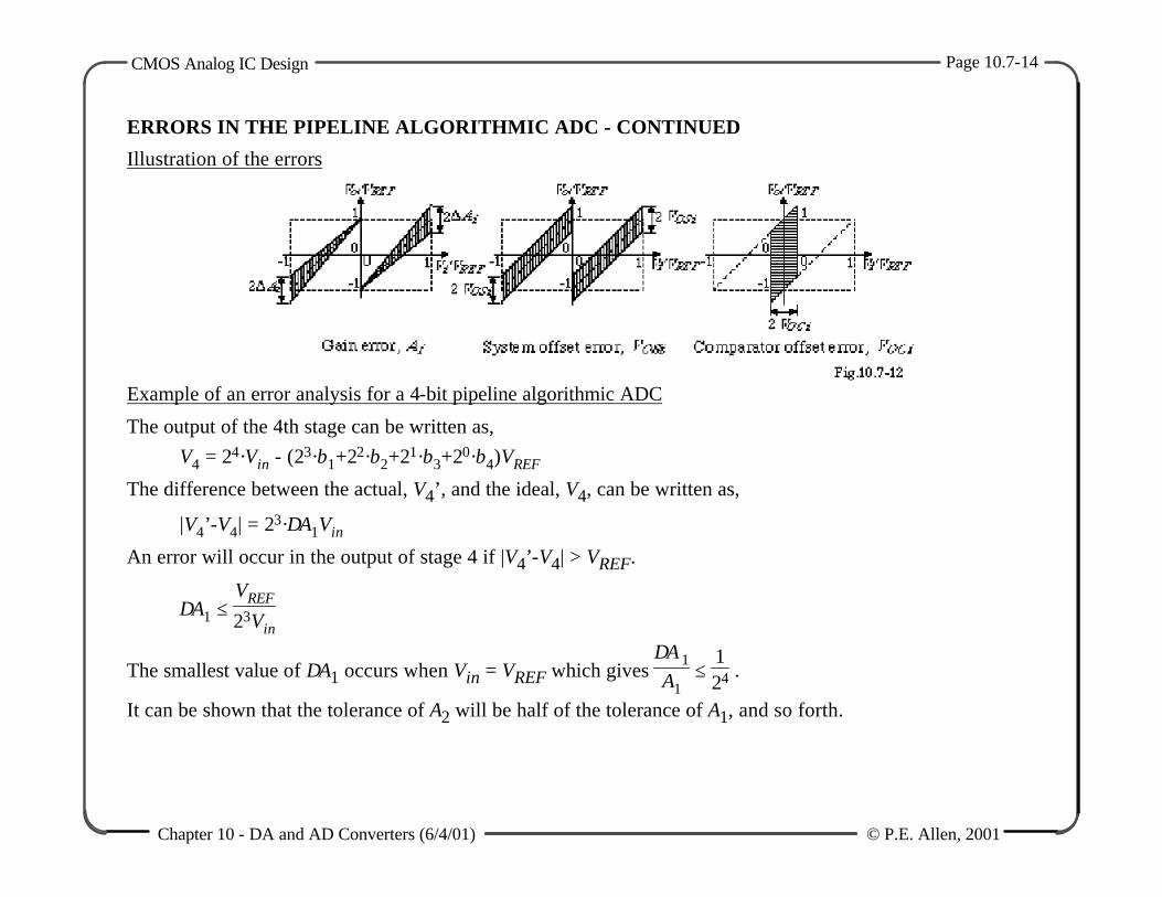
ERRORS IN THE PIPELINE ALGORITHMIC ADC - CONTINUED
Illustration of the errors
Example of an error analysis for a 4-bit pipeline algorithmic ADC
The output of the 4th stage can be written as, V4 = 24·Vin - (23·b1+22·b2+21·b3+20·b4)VREF
The difference between the actual, V4’, and the ideal, V4, can be written as,
|V4’-V4| = 23·∆A1Vin
An error will occur in the output of stage 4 if |V4’-V4| > VREF.
∴ ∆A1 ≤ VREF
23Vin
The smallest value of ∆A1 occurs when Vin = VREF which gives ∆Α1A1
≤ 124 .
It can be shown that the tolerance of A2 will be half of the tolerance of A1, and so forth.
CMOS Analog IC Design Page 10.7-15
Chapter 10 - DA and AD Converters (6/4/01) © P.E. Allen, 2001
Generally, ∆Α1A1
≤ 12N , VOS1 ≤
VREF
2N , and VOC1 ≤ VREF
2N

CMOS Analog IC Design Page 10.7-16
Chapter 10 - DA and AD Converters (6/4/01) © P.E. Allen, 2001
EXAMPLE 10.7-2 Accuracy requirements for a 5-bit pipeline algorithmic ADC
Show that if Vin = VREF, that the pipeline algorithmic ADC will have an error in the 5th bit if the gain of the first stage is 2-(1/8) =1.875 which corresponds to when an error will occur. Show the influence of Vin on this result for values of Vin of 0.65VREF and 0.22VREF.
Solution
For Vin = VREF, we get the following results shown in the table below. The input to the fifth stage is 0V which means that the bit is uncertain. If A1 was slightly less than 1.875, the fifth bit would be 0 which would be in error. This result of course assumes that all stages but the first are ideal.
i Vi(ideal) Bit i (ideal) Vi(A1=1.875) Bit i (A1=1.875) 1 1 1 1.000 1 2 1 1 0.875 1 3 1 1 0.750 1 4 1 1 0.500 1 5 1 1 0.000 ?
Now let us repeat the above results for Vin = 0.65VREF. The results are shown below. We see that now an error occurs in the fourth bit.
i Vi(ideal) Bit i (ideal) Vi(A1=1.875) Bit i (A1=1.875) 1 +0.65 1 0.6500 1 2 +0.30 1 0.2188 1 3 -0.40 0 -0.5625 0 4 +0.20 1 -0.1250 0 5 -0.60 0 0.7500 1
CMOS Analog IC Design Page 10.7-17
Chapter 10 - DA and AD Converters (6/4/01) © P.E. Allen, 2001
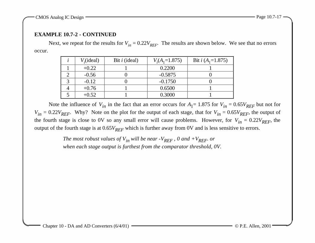
EXAMPLE 10.7-2 - CONTINUED
Next, we repeat for the results for Vin = 0.22VREF. The results are shown below. We see that no errors occur.
i Vi(ideal) Bit i (ideal) Vi(A1=1.875) Bit i (A1=1.875) 1 +0.22 1 0.2200 1 2 -0.56 0 -0.5875 0 3 -0.12 0 -0.1750 0 4 +0.76 1 0.6500 1 5 +0.52 1 0.3000 1
Note the influence of Vin in the fact that an error occurs for A1= 1.875 for Vin = 0.65VREF but not for Vin = 0.22VREF. Why? Note on the plot for the output of each stage, that for Vin = 0.65VREF, the output of the fourth stage is close to 0V so any small error will cause problems. However, for Vin = 0.22VREF, the output of the fourth stage is at 0.65VREF which is further away from 0V and is less sensitive to errors.
∴ The most robust values of Vin will be near -VREF , 0 and +VREF. or when each stage output is furthest from the comparator threshold, 0V.
CMOS Analog IC Design Page 10.7-18
Chapter 10 - DA and AD Converters (6/4/01) © P.E. Allen, 2001
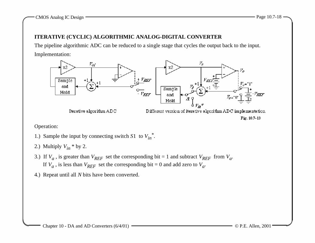
ITERATIVE (CYCLIC) ALGORITHMIC ANALOG-DIGITAL CONVERTER
The pipeline algorithmic ADC can be reduced to a single stage that cycles the output back to the input.
Implementation:
Operation:
1.) Sample the input by connecting switch S1 to Vin*.
2.) Multiply Vin * by 2.
3.) If Va , is greater than VREF set the corresponding bit = 1 and subtract VREF from Va. If Va , is less than VREF set the corresponding bit = 0 and add zero to Va.
4.) Repeat until all N bits have been converted.

CMOS Analog IC Design Page 10.7-19
Chapter 10 - DA and AD Converters (6/4/01) © P.E. Allen, 2001
EXAMPLE 10.7-3
Conversion Process of an Iterative, Algorithmic Analog-Digital Converter
The iterative, algorithmic analog-digital converter is to be used to convert an analog signal of 0.8VREF. The figure below shows the waveforms for Va and Vb during the process. T is the time for one iteration cycle.
1.) The analog input of 0.8VREF givesVa = 1.6VREF and a value of Vb = 0.6VREF and the MSB as 1.
2.) Vb is multiplied by two to give Va = 1.2VREF. Thus the next bit is also 1 and Vb = 0.2VREF..
3.) The third iteration givesVa = 0.4VREF, making the next bit 0 and Vb = 0.4VREF .
4.) The fourth iteration gives Va = 0.8VREF, which gives Vb = 0.8VREF and the fourth bit as 0.
5.) The fifth iteration gives Va = 1.6VREF, Vb = 0.6VREF and the fifth bit as 1.
The digital word after the fifth iteration is 11001 and is equivalent to an analog voltage of 0.78125VREF.

CMOS Analog IC Design Page 10.7-20
Chapter 10 - DA and AD Converters (6/4/01) © P.E. Allen, 2001
SELF-CALIBRATING ANALOG-DIGITAL CONVERTERS
Self-calibration architecture for a m-bit charge scaling, k-bit voltage scaling successive approximation ADC
Comments:
• Self-calibration can be accomplished during a calibration cycle or at start-up
• In the above scheme, the LSB bits are not calibrated
• Calibration can extend the resolution to 2-4 bits more that without calibration
CMOS Analog IC Design Page 10.7-21
Chapter 10 - DA and AD Converters (6/4/01) © P.E. Allen, 2001
CMOS Analog IC Design Page 10.7-22
Chapter 10 - DA and AD Converters (6/4/01) © P.E. Allen, 2001
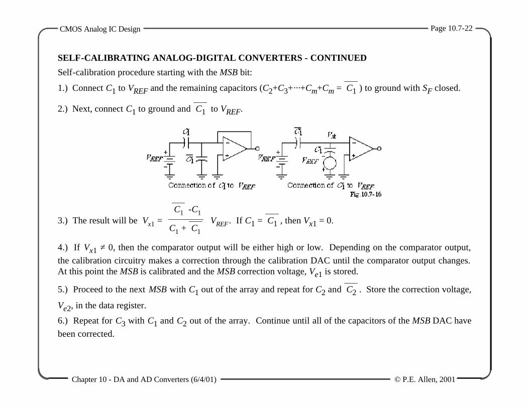
SELF-CALIBRATING ANALOG-DIGITAL CONVERTERS - CONTINUED
Self-calibration procedure starting with the MSB bit:
1.) Connect C1 to VREF and the remaining capacitors (C2+C3+···+Cm+Cm = C1 ) to ground with SF closed.
2.) Next, connect C1 to ground and C1 to VREF.
3.) The result will be Vx1 =
C1 -C1
C1 + C1
VREF. If C1 = C1 , then Vx1 = 0.
4.) If Vx1 ≠ 0, then the comparator output will be either high or low. Depending on the comparator output, the calibration circuitry makes a correction through the calibration DAC until the comparator output changes. At this point the MSB is calibrated and the MSB correction voltage, Vε1 is stored.
5.) Proceed to the next MSB with C1 out of the array and repeat for C2 and C2 . Store the correction voltage,
Vε2, in the data register.
6.) Repeat for C3 with C1 and C2 out of the array. Continue until all of the capacitors of the MSB DAC have been corrected.
CMOS Analog IC Design Page 10.7-23
Chapter 10 - DA and AD Converters (6/4/01) © P.E. Allen, 2001
Note that for any combination of MSB bits the calibration circuit adds the correct combined correction voltage during normal operation.
CMOS Analog IC Design Page 10.7-24
Chapter 10 - DA and AD Converters (6/4/01) © P.E. Allen, 2001
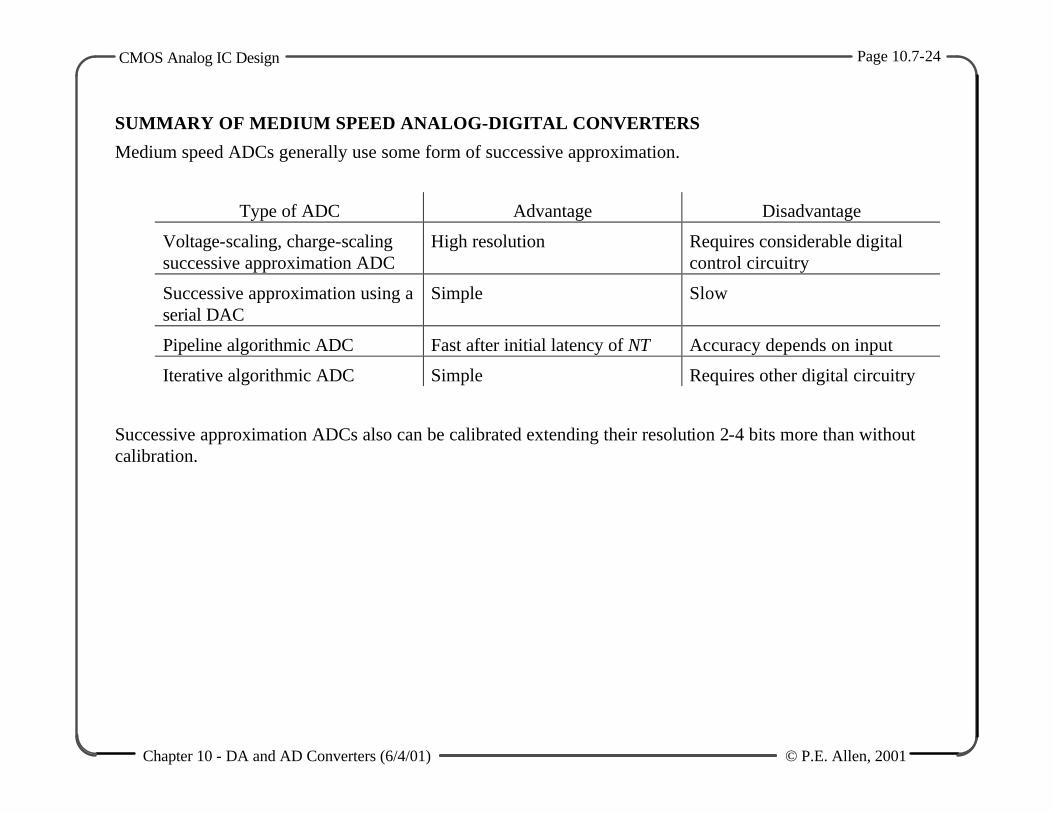
SUMMARY OF MEDIUM SPEED ANALOG-DIGITAL CONVERTERS
Medium speed ADCs generally use some form of successive approximation.
Type of ADC Advantage Disadvantage
Voltage-scaling, charge-scaling successive approximation ADC
High resolution Requires considerable digital control circuitry
Successive approximation using a serial DAC
Simple Slow
Pipeline algorithmic ADC Fast after initial latency of NT Accuracy depends on input
Iterative algorithmic ADC Simple Requires other digital circuitry
Successive approximation ADCs also can be calibrated extending their resolution 2-4 bits more than without calibration.