1 Interconnect and Packaging Lecture 7: Distortionless Communication Chung-Kuan Cheng UC San Diego.
date post
21-Dec-2015Category
view
213download
0
1
Interconnect and PackagingLecture 2: Scalability
Chung-Kuan ChengUC San Diego

2
Outlines
I. Trends of Interconnect and Packaging
II. Scalability
References

3
I. Trends of High Performance Interconnect and Packaging
Year 2005 2010 2015
D1/2 Pitch nm 80 45 25
Chip size (mm2) 310 310 310
Pin count 3,400 4,009 6,402Cents/pin 1.78 1.37 1.05
On-chip (MHz) 5,170 12,000 -
Off-chip (MHz) 3,125 - 29,103
Power Density (w/mm2)
0.54 0.64 -

4
I. Trends
• On-Chip Interconnect
• Delay (5-40 times of Speed of Light 5ps/mm)
• Power Density (> ½)
• Clock Skew: Variations (5GHz)
• Off-Chip Interconnect and Packaging• Number of pins (limited growth)
• Wire density (scalability)
• Speed and distance of interconnect

5
I. Trends
• On-chip Global Interconnect trend
• Concerns: Speed, Power, Cost, Reliability
0
40
80
120
160
200
180 150 130 100 90 80 70 65 57 50Process Technology Node (nm)
Dela
y (p
s)
1mm Global I nterconnect with Scattering(source: I TRS Roadmap 2004)
FO4 I nverter Delay (Estimated by0.36*Ldraw)
1mm distortionless Transmission Line (Speedof Light)
6
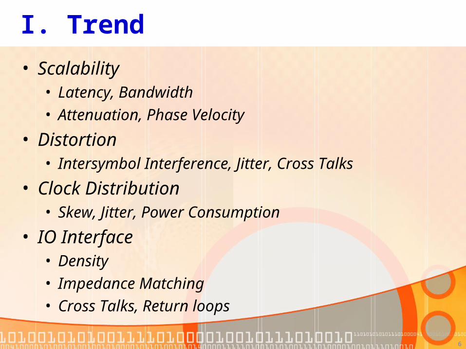
I. Trend
• Scalability• Latency, Bandwidth• Attenuation, Phase Velocity
• Distortion• Intersymbol Interference, Jitter, Cross Talks
• Clock Distribution• Skew, Jitter, Power Consumption
• IO Interface• Density• Impedance Matching• Cross Talks, Return loops

7
II. Scalability: Interconnect Models
RΔl LΔlCΔl
RΔl LΔl
CΔl …
i(z,t)
RΔl LΔl RΔl LΔl
Voltage drops through serial resistance and inductance
Current reduces through shunt capacitance
Resistance increases due to skin effect
Shunt conductance is caused by loss tangent

8
II. Scalability: Interconnect Models• Telegrapher’s equation:
),(),(),(
),(),(
),(
tzGVdt
tzdVC
dz
tzdIdt
tzdILtzRI
dz
tzdV
• Propagation Constant:
jCjGLjR ))((
• Wave Propagation:
//,),( 0 tzveVtzV tjzjz
• Characteristic Impedance
)/()( CjGLjRZ

9
II. Scalability of Physical Dimensions• R= p /A = p/(wt)• Z= ¼ (u/e)1/2 ln (b+w)/(t+w)• C= v Z• L= Z/v
b
w
t
p: resistivity of the conductoru: magnetic permeabilitye: dielectric permittivityv: speed of light in the medium

10
II. Scalability of Physical Dimensions • Resistance: Increases quadratically with
scaling, e.g. p=2um-cm
R=0.0002ohm/um at A=10umx10um
R=0.02ohm/um at A=1umx1um
R=2ohm/um at A=0.1umx0.1um
• Characteristic Impedance: No change
• Capacitance per unit length: No change
• Inductance per unit length: No change

11
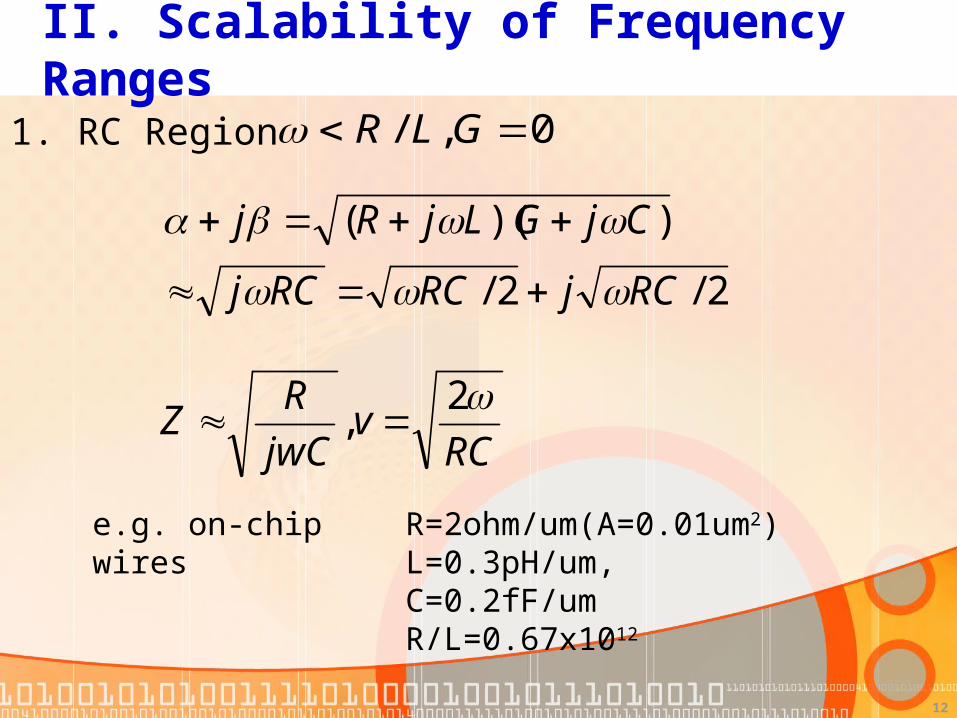
II. Scalability of Frequency Ranges
1. RC Region
2. LC Region
3. Skin Effect
4. Loss Tangent
12
II. Scalability of Frequency Ranges
2/2/
))((
RCjRCRCj
CjGLjRj
1. RC Region 0,/ GLR
RCv
jwC
RZ
2,
e.g. on-chip wires R=2ohm/um(A=0.01um2)L=0.3pH/um, C=0.2fF/umR/L=0.67x1012

13
II. Scalability of Frequency Ranges: RC Region
gw
w
wg
ns
sclcc
lrr
lcsfcc
srr
2/
2/
/
2
1
1
Elmore delay model with buffers inserted in intervals
ltr: length from transmitter to receiverl: interval between buffersrn: nmos resistancecn: nmos gate capacitancecg=(1+g)cn, g is pn ratio.rw: wire resistance/unit lengthcw: wire capacitance/unit lengthf: cd/cg
l
ltr
l
llscrl
crcfslc
s
rlDelay tr
gwww
gwn
tr }2
))1(({)( 2

14
II. Scalability of Frequency Ranges: RC Region
l
llscrl
crcfslc
s
rlDelay tr
gwww
gwn
tr }2
))1(({)( 2
ww
gn
cr
crfl
)1(2
gw
wn
cr
crs
Elmore delay model with buffers inserted in intervals
Optimal interval
wgwntrtr ccrrfllDelay ))1(22(/)(
Optimal buffer size
Optimal delay

15
II. Scalability of Frequency Ranges
mcr
crfl
ww
gn 242)1(2
41gw
wn
cr
crs
Example: w= 85nm, t= 145nm
Optimal interval
mmpsmfsccrrfllDelay wgwntrtr /194/194))1(22(/)(
Optimal buffer size
Optimal delay
rn= 10Kohm,cn=0.25fF,cg=2.34xcn=0.585fFrw=2ohm/um, cw=0.2fF/um

16
II. Scalability of Frequency Ranges: RC Region
Year
(On-Chip)
2005 2010 2015
rncn (ps) 0.86 0.39 0.18
rwcw (ps/mm)* 284 616 1510
l (um) 168 77 33
D (ps/um) 0.096 0.095 0.101
*no scattering, p=2.2uohm-cm

17
II. Scalability of Frequency Ranges: RC Region
• Device delay, rncn, decreases with scaling
• Wire delay, rwcw, increases with scaling
• Interval, l, between buffers decreases with scaling
• In order to increase the interval, we add the stages of each buffer.

18
II. Scalability of Frequency Ranges2. LC Region 0,/ GLR
LCjZ
RCjLjR
CjGLjRj
2)(
))((
LCvCLZ /1,
19
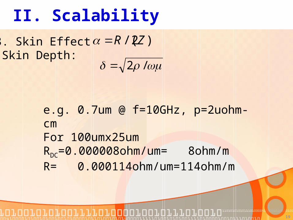
II. Scalability
3. Skin Effect Skin Depth:
/2
)2/( ZR
e.g. 0.7um @ f=10GHz, p=2uohm-cmFor 100umx25umRDC=0.000008ohm/um= 8ohm/mR= 0.000114ohm/um=114ohm/m

20
II. Scalability4. Loss Tangent
tan),tan1( 0,00 CGCCj
)(/62/,02.0tan polyimidemGZp
)(/6.02/,002.0tan glassmGZg )(/06.02/,0002.0tan quartzmGZq
LCjGZ
Z
R
CjGLjRj
22
))((

21
References• E. Lee, et al., “CMOS High-Speed I/Os – Present and Future,” ICCD
2003.• http://www.itrs.net/Common/2004Update/2004Update.htm• G.A. Sai-Halasz G.A. "Performance Trends in High-End Processors,“
IEEE Proceedings, pp. 20-36, Jan. 1995.• M.T. Bohr, “Interconnect scaling-the real limiter to high performance
ULSI” Electron Devices Meeting, 1995., International10-13 Dec. 1995 pp.241 – 244.