
1 Chapter 2. Basic Semiconductor Physics 9/12/2008.
76
1 Chapter 2. Basic Semiconductor Physics 9/12/2008
-
Upload
ralf-harmon -
Category
Documents
-
view
223 -
download
0
Transcript of 1 Chapter 2. Basic Semiconductor Physics 9/12/2008.

1
Chapter 2. Basic Semiconductor Physics
9/12/2008

2
2.1 Introduction
• Si, GaAs, InP: the published experimental and theoretical values of certain parameters differ considerably from reference to reference.
• Even worse for less matured materials (e.g., SiC or GaN), alloys and strained layers.
• The 11 basic semiconductors: the cubic crystal type (Ge, Si, GaAs, AlAs, InAs, InP, GaP), the hexagonal (wurtzite) crystal type (SiC (4H & 6H), GaN, AlN).
• A linear interpolation scheme used for approximating material parameters unavailable.

3
• If the material parameters are known for 2 basic binary compounds AC & BC, the composition-dependent material parameter TAxB1-xC(x) of the ternary compound (AxB1-xC) can be estimated by
• For a quaternary alloy of composition AxB1-xCyD1-y,
• This method is valid only when reliable data for the alloy of interest are not available.
• Although numerical device simulation accounts for more physical effects and is often more accurate, analytical approaches nonetheless enjoy great popularity.
BCACCBA BxxBxTxx
)1()(1
BDBCADACDCBA ByxyBxByxxyByxQyyxx
)1)(1()1()1(),(11

4
2.2 Free-Carrier Densities
2.2.1 Band diagrams and Band structure• Carrier density=the number of carriers/cm3
• Under the thermal equilibrium condition, heat is only energy applied to the semiconductor.
• If other types of energy are applied, the equilibrium may be perturbed. nonequilibrium
• EG = EC – EV (Energy state ≈ Energy level)

5

6
• Generation: the electron is lifted to the conduction band, leaving behind an unoccupied state in the valence band.
• Recombination: a free electron falls down from the conduction band to the valence band, thereby releasing energy (≥ the bandgap) and filling the hole.
• At T=0 K, all allowed states below EF are filled with electrons and all states above EF are empty.
• The density of electrons and holes can also be increased by intentionally incorporating impurities (dopants) into the semiconductor.

7
• Energy band structure

8
2.2.2 Carrier Statistics
• The density of states (the density of allowed energy states) in the conduction band, N(E):
mn,ds: the density-of-states effective electron mass.
• The effective density of states in the conduction band, NC, defined as
• Therefore,
2/1
2/3
2, )(
24)( c
dsn EEh
mEN
2/3
2
,22
h
TkmN Bdsn
C
TkTk
EENEN
BB
CC
12)(
2/1

9
• The probability that E is occupied by an electron is governed by the Fermi-Dirac distribution function f(E): (2-6)
At E = EF, f(E) is ½.
• The density of electrons at a certain energy: the density of states × the occupation probability =
(2-7)
Tk
EE
B
F
e
Ef
1
1)(
0
1/ 2
( ) ( )
2 1 1
1 exp
C
C
E
C F
EB BF
B
n N E f E dE
N E EdE
k T k TE Ek T

10
• Changing the variable from E to x with
(2-10)
Fermi integral of the order ½, which unfortunately cannot be solved analytically.
• Similarly, the hole density in valence band:
C
B
E Ex
k T
0 0
2
1 exp
C
F C
B
N xn dx
E Ex
k T
1/ 2
3/ 2
,
2
2 1( )
22
VV
B B
h ds BV
E Ep E N
k T k T
m k TN
h

11
• The probability that the energy state is empty, i.e., not occupied by and electron:
• After some algebraic manipulations,
(2-14)
1( ) 1 ( ) 1
1 exph
F
B
f E f EE E
k T
0 0
2 where
1 exp
V V
BV F
B
N E Exp dx x
k TE Ex
k T

12
2.2.3 Approximations for the Carrier Densities
• Boltzmann Statistics– For E-EF>3kBT, the exponential term in (2-6) is >>1,
(2-16)
– Similarly, for EF-E>3kBT
– f(E) and fh(E) are called the Boltzmann distribution functions. (2-5)&(2-16)(2-7):
(2-18)
( ) exp F
B
E Ef E
k T
( ) exp Fh
B
E Ef E
k T
0
0
exp
exp
C FC
B
F VV
B
E En N
k T
E Ep N
k T

13
– Semiconductors with above conditions are nondegenerate.
– For degenerate semiconductors (n-type with E-EF< 3kBT and p-type with EF-E<3kBT), the Fermi-Dirac statistics should be used.
– Nondegenerate and degenerate semiconductors correspond to lightly and heavily doped materials, respectively.
– The electron density = the hole density in an intrinsic semiconductor
0
0
exp
exp
C Fi C
B
F Vi V
B
E En n N
k T
E Ep n N
k T

14

15
– Solving the above equations for NC and NV, inserting the results into (2-18),
– Under thermal equilibrium mass action law
– The charge neutrality is maintained in any semiconductor device regardless of the doping. (Electrons and holes are mobile charges, whereas ionized dopants are fixed.)
0
0
exp
exp
F ii
B
i Fi
B
E En n
k T
E Ep n
k T
20 0 exp G
i C VB
En p n N N
k T
D Ap N n N

16
• Complete Dopant Ionization-Approximation 1– Assume all donors are ionized in an n-type material and
the dopant concentration>>ni n0 ≈ ND,
– Similarly, for a p-type, p0 ≈ NA,
• Complete Dopant Ionization-Approximation 2– Low doping or a large intrinsic carrier concentration
– In an n-type material,
(2-30)
2
0i
D
np
N
2
0i
A
nn
N
2
0 00
2 2 2 2
0 0
4 4,
2 2
iD D
D D i D i D
nn N p N
n
N N n N n Nn p

17
– Similarly, for a p-type,
• Incomplete Dopant Ionization– The dopant atoms are not 100% ionized. – ND>ND
+ in n-type, NA>NA- in p-type.
– This occurs either at low temperature or when the dopant’s activation energy is high.
– At room temperature, complete ionization can be assumed for most semiconductors, e.g., Si, GaAs, and InGaAs.
– In SiC, EDA and EAA are larger than those in the above-mentioned materials, and at room temperature only a portion of the dopants are ionized.
2 2 2 2
0 0
4 4,
2 2A A i A i AN N n N n N
p n

18
– For n-type, the density of ionized donors with EDA and ED is described using the Fermi-like distribution function:
ground state degeneracy factor g is added.
– The density of ionized donors (i.e., the density of donor states not occupied by an electron) can be:
(2-37)
1
11 exp
D
D F
B
fE E
g k T
1(1 ) 1
11 exp
D D D D
D F
B
N N f NE E
g k T

19
– Assuming the electron density ≈ the density of ionized donors, (2-37) (2-38)
– Rearranging (2-18)
– Insert this into (2-38) and solving a quadratic equation
– The density of ionized acceptors:
– The probability fA of an acceptor state occupied by an electron can be:
0
1
1 expD
F D
B
n NE E
gk T
0lnF B CC
nE k T E
N
0 exp 1 4 exp 12
C C D C DD
B C B
N E E E ENn g
g k T N k T
A A AN N f
1
1 expA
A F
B
fE E
gk T

20
– Finally, using (2-19)
• Joyce-Dixon Approximation
0 exp 1 4 exp 12
V A V A VA
B V B
N E E E ENp g
g k T N k T
2 3 4
0 0 0 0 01 2 3 4
2 3 4
0 0 0 0 01 2 3 4
ln
ln
F C
B C C C C C
V F
B V V V V V
E E n n n n na a a a
k T N N N N N
E E p p p p pa a a a
k T N N N N N

21

22
2.3 Carrier Transport
2.3.1 Introduction
• 2 driving forces for carrier transport: electric field and spatial variation of the carrier concentration.
• Both driving forces lead to a directional motion of carriers superimposed on the random thermal motion.
• To calculate the directional carrier motion and the currents in a semiconductor, classical & nonclassical models can be used.
• The classical models assume that variation of E-field in time is sufficiently slow so that the transport properties of carriers (mobility or diffusivity) can follow the changes of the field immediately.

23
• If carriers are exposed to a fast-varying field, they may not be able to adjust their transport properties instantaneously to variations of the field, and carrier mobility and diffusivity may be different from their steady-state values nonstationary
• Nonstationary carrier transport can occur in electron devices under both dc and ac bias conditions.
• Whether the field acting on the carrier is varying in time or nor is important.
• In III-V transistors, nonstationary transport plays an important role, but is much less important in Si transistors. In SiC transistors, it is entirely neglected.

24
2.3.2 Classical Description of Carrier Transport
A. Carrier Drift.
• Assume thermal equilibrium for a semiconductor having a spatially homogeneous carrier concentration with no applied E-field. No driving force for directional carrier motion. The carriers not in standstill condition but in continuous motion due to kinetic energy. For electron in the conduction band, where vth is the thermal velocity, mn* is the conductivity effective electron mass.
• The average time btw 2 scattering events is the mean free time and the average distance a carrier travels btw collisions is the mean free path. Fig. 2.5 (a)
• Applying V, the E-fields adds a directional component to the random motion of the electron. Fig. 2.5 (b)
*23
2 2n
kin B th
mE k T v

25
• The mean electron velocity: vn= -μnE
• The directed unilateral motion of carriers caused by E-field is drift velocity.
• Similarly, vp = μpE
• A change in E-field instantaneously results in a change of the drift velocity.

26
• Band diagram: qV=ΔEC= ΔEV= ΔEi= ΔEF

27
B. Low-Field Carrier Drift.
• The drift velocity is linearly dependent on the field.
• The low-field mobilities μ0n and μ0p depend on both the doping concentration and on the temperature.
• The dependence of the low-field mobility is modeled empirically
ref
minmaxmin0
1NN

28
• The mobility of minority carriers can be considerably higher than that of majority carriers.
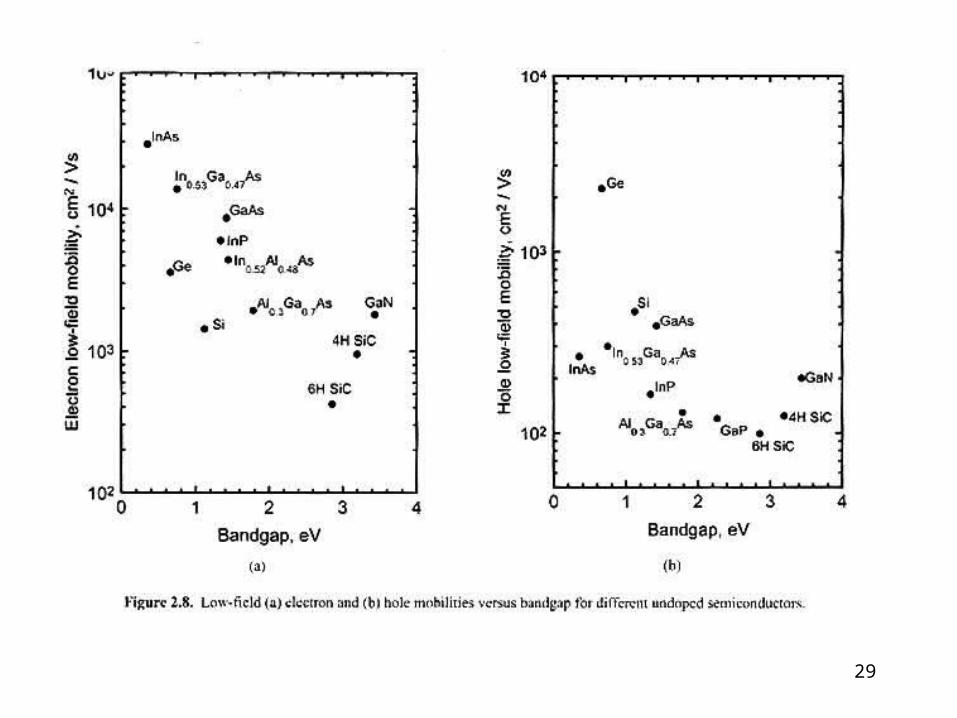
• The electron low-field mobilities for Si and GaAs in Fig 2.7
• The low-field electron and hole mobilities of different undoped semiconductors in Fig 2.8
29

30
• Temperature-dependent low-field mobility
n
K
TKT
300)300()( 00

31
C. High-Field Carrier Drift• v-E characteristics for Si and for semiconductors
with similar v-E characteristics can be modeled by the empirical expression
• The saturation velocity vsat is temperature-dependent and decreases with increasing temperature. For electrons and holes in Si,
1/
0
0
sat
1( )
1
v
v
E EE
scm
KT
v /
600exp8.01
104.2 7
sat

32

33
• In GaAs or InP, not only can a sublinear slope of the v-E characteristics be observed, but the velocity actually decreases after reaching a peak value at a certain critical field and approaches asymptotically to a saturation value.
• Fig 2.11 illustrates the electron population in the lower and upper valleys and the stationary v-E characteristics for GaAs.

34

35
D. Drift Current Densities
• The drift current density JDr is described by the product of the density, the charge, and the drift velocity of the drifting carriers.
• Under low-field conditions where v = μ0E holds,
• The total drift current density JDr = JDr,n +JDr,p.
Dr,
Dr,
( )
( )n n n
p p p
J qnv qn
J qnv qn
E E
E E
Dr, 0
Dr, 0
n n
p p
J qn
J qn
E
E
36
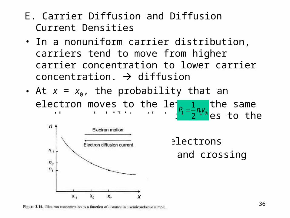
E. Carrier Diffusion and Diffusion Current Densities
• In a nonuniform carrier distribution, carriers tend to move from higher carrier concentration to lower carrier concentration. diffusion
• At x = x0, the probability that an electron moves to the left is the same as the probability that it moves to the right.
• The average rate P1 of electrons flowing from x1 toward x0 and crossing the plane x = x0 is
thvnP 11 2
1

37
• Approximating the concentration at x1,
• Analogously, the average rate of electrons flowing from x-1 toward x0 is
• The net rate P of electrons crossing the plane at x0 in +x direction is the difference btw P-1 and P1,
• Introducing the electron diffusion coefficient Dn=vthΔx,
• The electron diffusion current density JDi,n can be obtained from the net rate of electron diffusion by multiplying P with the charge of an electron, i.e., by –q, as
xnvP dxdn
th 01 2
1
xnvP dxdn
th 01 2
1
xvP dxdn
th
dx
dnDP n
dx
dnqDJ nn ,Di

38
• Similarly,
• JDi = JDi,n + JDi,p
• Driving force for a diffusion current is the gradient of the carrier concentration, whereas the driving force for a drift current is the electric field.
• The main difference btw these driving forces is that the field acts directly on the carriers and give rise to a directional motion of every carrier in the sample, whereas an individual carrier does not feel any force from a carrier concentration gradient.
• A relationship btw mobility and diffusion coefficient Einstein relation: (2-70)
dx
dpqDJ pp ,Di
pB
pnB
n q
TkD
q
TkD ,

39
F. Alternative Expressions for the Current Density
• Since ,
• Similarly,
• Therefore, the general driving force for a current is the gradient of the Fermi level, and it is impossible to identify from whether this driving force is caused by a field or a gradient of the carrier concentration.
Dr, Di, Dr, Di,
Dr, Di,
n n p p
n n n n n
J J J J J
dnJ J J qn qD
dx
E
, F
dE E q
dx
E
exp
n n n
F in n i
B
Fn
dnJ qn qD
dx
E Ed dqn qD n
dx dx k T
dEn
dx
E
dx
dEpJ F
pp

40
2.3.3 Nonclassical Description of Carrier Transport
• The basic assumption of the classical description of carrier drift a sudden change of the field results in an immediate change of carrier drift velocity: Not correct!!
• According to classical mechanics, a particle with a certain mass cannot change its velocity instantaneously because of inertia, even if the driving force for the motion does.
• Carriers possess a certain mass (the effective mass) and need a certain transition time to change their kinetic energy and their velocity after a sudden variation of the field.
• The behavior of carriers during the transition period is called carrier dynamics or nonstationary carrier transport.
• Such a transport was first investigated using Monte Carlo Simulation for Si and GaAs.

41
• It can also be described easily by the relaxation time approximation (RTA). The heart of the RTA is the energy and momentum balance equations, for a homogeneous semiconductor:where
τE and τp: the energy-dependent effective relaxation times
for carrier energy and momentum,
E0: the carrier energy at thermal equilibrium (E = 0),m*: the conductivity effective electron mass (the effective mass related to transport phenomena),m*×v : momentum P of the carrier.
• The balance btw the amount of energy and momentum that carriers gained from the applied field, and the energy and momentum loss caused by scattering. The effects of all different scattering events are combined in τE
and τp
0 ( * ) *,
E p
E EdE d m v m vq v q
dt dt
E E

42
• Stationary v-E, E-E, and m*-E are needed to simulate nonstationary transport.
• Let us consider an n-type GaAs sample, at time t, the electron possess E(t), P(t) and m*(t) and travel with v(t). Now assume that during the small time interval Δt after t the applied field changes from E(t) to E(t+Δt). The evolution of the electron velocity: – Calculate τE(t+Δt) and τP(t+Δt) by assuming stationary conditions
(d/dt=0)
– Calculate the electron energy and momentum at t+Δt. For this, the balance equations are discretized.
*0( ) ( )
( ) , ( )( ) ( ) ( )
st st stE p
st st st
E t E m t vt t t t
q t v t q t
E E
)(
)()()()(
)(
)()()()()( 0
tt
tPttqEttPttP
tt
EtEtvttqEttEttE
P
E

43

44
– Set Est(t+Δt) = E(t+Δt) and deduce the new stationary values Est(t+Δt), vst(t+Δt) and mst*(t+Δt) from Fig 2.15
– Calculate the electron velocity v(t+Δt) from
– Increase the time by another Δt and proceed with step 1.
)(
)()(
* ttm
ttPttv
st
45
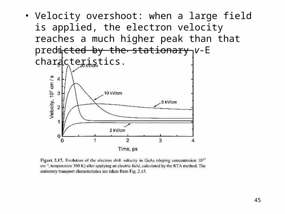
• Velocity overshoot: when a large field is applied, the electron velocity reaches a much higher peak than that predicted by the stationary v-E characteristics.

46
2.4 PN Junctions

47
• In Fig.2.18, the field is in –x direction and is the driving force for a drift current. This drift tendency is in the opposite direction of the diffusion tendency. With no bias applied to the pn junction, the diffusion and drift tendencies compensate each other, and no net carrier flow occurs.
• The electron affinity χ is the energy difference btw the vacuum level and the conduction band edge.
• The energy barrier btw the p- and n-type regions is the same for the conduction and valence bands built-in voltage Vbi of the pn junction.
• Derivation of Vbi: When no external voltage is applied, no net current flows across the junction.
(2-84)Dr, Di, 0n n n n n
dnJ J J q n qD
dx E

48
• Rearranging (2-84) and applying Einstein relation (2-70)
• Integrating across the space-charge region (-xp ~ xn),
• To find the thickness of the space-charge region, using Poisson equation, where ε = ε0εr
0 0n n n B n
B
q n dx qD dn q n dx k T dn
k T dnd dx
q n
E E
E
2 2
( )ln
( )
ln ln/
n n
p p
x xnB B
bi x xp
B D B D A
i A i
n xk T dn k TV d
q n q n x
k T N k T N N
q n N q n
2
2( )D A
d d qp n N N
dx dx
E

49
• In the space-charge region on the p-type side, simplified to
• Applying the boundary condition, i.e., E-field = 0 at x=-xp,
(2-89)
• Similarly, on the n-type side,
(2-90)
2
2 A
d qN
dx
( )A p
qN x x
E
( )A n
qN x x
E

50
• Integrating (2-89) & (2-90) gives the potential distribution, using B.C. (φ=0 at x=-xp, φ=Vbi at x=xn),
• Because the potential in a pn junction is continuous,
the thickness of the space-charge region under the thermal equilibrium (no voltage is applied)
2
2
( ) ( ) on the p-type side,2
( ) ( ) on the n-type side2
A p
bi D n
qx N x x
qx V N x x
(0 ) (0 ), (0 ) (0 )
2 2,
( ) ( )bi biD A
p nA D A D D A
V VN Nx x
q N N N q N N N
2 bi D Asc p n
D A
V N Nd x x
q N N

51
• For the case of a voltage applied,
• We next discuss the minority carrier concentrations at the edges of the space-charge region.
• If no external voltage is applied, n(-xp) = n0p, p(xn) = p0n.• Under forward-bias condition (Vpn>0), the drift and
diffusion currents no longer compensate each other.• The extrinsic field caused by the applied voltage is in the
opposite direction compared to the intrinsic field originated from the uncompensated acceptor and donor ions in s-c region.
2 ( ) 2 ( ),
( ) ( )bi pn bi pnD A
p nA D A D D A
V V V VN Nx x
q N N N q N N N
2 ( )bi pn D Asc p n
D A
V V N Nd x x
q N N

52
• Thus, the resulting field is smaller compared to that of the equilibrium case, the drift current is decreased, and the diffusion current becomes the dominant tendency. injection of electrons from n-type to p-type, and holes are injected into n-type region. minority carrier concentrations in the s-c region and at the edges of s-c region are increased.
• Fermi level is no longer a straight line across the pn junction. no longer single Fermi level, Eqs. (2-22)&(2-23) are not valid. quasi-Fermi levels are introduced. split into 2 separate quasi-Fermi levels for Efn and Efp.
(2-99)
(2-100)
exp
exp
Fn ii
B
i Fpi
B
E En n
k T
E Ep n
k T

53
• Multiplying above 2 eqs,
(2-101)
2 2 2exp , exp expFn Fp pn pni i i
B B T
E E qV Vnp n p n n
k T k T V

54
• For a forward bias applied to the pn junction, Eqs. (2-99)-(2-101) result in increased minority carrier densities in the entire space-charge region.
• In the p-type bulk region, electrically neutral Δn= Δp even true at the edge of s-c region.
• In most cases, n0p is much smaller compared to the other charge components.
0 0( ) ( )p p p pp x p n x n
0 0 20 0
0
4( ) 1 exp 1 since
2p p pn
p i p pp T
p n Vn x n n p
p V

55
• Similarly, for the minority carrier density at x=xn,
• For low-level injection, i.e., for small Vpn ((1+x)n≈1+nx) and low injected minority carrier densities,
• For high-level injection, (large Vpn)
0 0
0
4( ) 1 exp 1
2pnn n
nn T
Vn pp x
n V
2
0
2
0
( ) exp exp
( ) exp exp
pn pnip p
T A T
pn pnin n
T D T
V Vnn x n
V N V
V Vnp x p
V N V
( ) exp2
( ) exp2
pnp i
T
pnn i
T
Vn x n
V
Vp x n
V

56
• At x=-xp, E=0, assuming no recombination taking place,
(2-111)
Di, Di,
Di, Di,
( ) ( )
( ) ( )
p n
n p p p
n p p n
n px x
J J x J x
J x J x
dn dpqD qD
dx dx

57
• The characteristic lengths Ln and Lp are minority carrier diffusion lengths for electrons and holes. This is the average distance an excess minority carriers can move by diffusion in a sea of majority carriers before they disappear by recombination.
• Defined as
where Dn and Dp: the minority electron and hole diffusion coefficients, τn and τp : the minority electron and hole lifetimes.
• To determine (2-111), assume a 1st order approximation.
,n n n p p pL D L D
0 0( ) ( )p p n n
n pn n
n x n p p xJ qD qD
L L

58
• Assuming complete ionization, (2-27),(2-29), (2-105) and (2-106),
Valid for the long-base junction
• Junctions with quasineutral regions shorter than the minority carrier diffusion lengths are short-base junctions.
2 2
exp 1pni in p
A n D n T
Vn nJ q D D
N L N L V
2 2
exp 1 exp 1( ) ( )
pn pni in p s
A Bp p D Bn n T T
V Vn nJ q D D J
N x x N x x V V

59
• A rectifying junction formed by a metal and a semiconductor.
• For microwave transistors, the most important Schottky junction is the junction btw a metal and an n-type semiconductor serving as a gate electrode in MESFETs and HEMTs.
2.5 Schottky Junctions

60
• In real Schottky junctions, there are charged interface states located at the metal-semiconductor interface, and the effect of the interface states on the behavior of the Schottky junction is typically more significant compared to that of the work function difference itself.
• Although many theories for the Schottky junction have been proposed, commonly the Vbi is not calculated using an expression derived from a physical mode, but rather is taken from experimental data.
• A quantity closely related to Vbi is the Schottky barrier height φb. ( )bi b C FqV E E

61

62
• Thickness of the space-charge region: using Poisson equation,
– First, consider the zero applied voltage using the boundary conditions that at x = dsc, E =0, φ = Vbi.
– Since φ = 0 at x = 0,
– With Vapp,
2
2
( ) Dd x qN
dx
2( ) ( )2
Dbi sc
qNx V x d
2 bisc
D
Vd
qN
2 ( )bi appsc
D
V Vd
qN

63
2.6 Impact Ionization
• Carriers in a semiconductor are accelerated and pick up energy when E-field is applied.
• During the scattering process, they transfer part of the energy to the lattice.
• If the field is sufficiently high, a carrier can gain so much energy that during a collision with the lattice it can break a bond and create a free electron. Due to the energy transfer, a valence electron is moved to the conduction band, thereby creating a free electron and a free hole.
• As a result, an electron-hole pair is generated and we have 3 carriers after the scattering event compared to only 1 carrier before the process. Impact ionization

64
• The sum of the energies of the 3 carriers after scattering = the energy of the original carrier before scattering.
• The same holds for the momentum.• After impact ionization, all 3 carriers are
accelerated by the field. If the field remains high enough, they can create further electron-hole pairs, which are again accelerated and create more electron-hole pairs. An enormous increase in the total number of carriers is the avalanche multiplication.
• Avalanche can lead to device breakdown, and, if the currents are not limited, may destroy the device.

65
• The voltage at which avalanche becomes noticeable is the breakdown voltage BV.
• Obviously the minimum kinetic energy a carrier must gain to cause impact ionization is slightly larger than the bandgap energy.
• The increase in carrier concentration by impact ionization is described by the electron-hole pair generation rate GII defined by
where αn and αp: the electron and hole ionization rates = the number of electron-hole pairs generated by an electron (hole) per unit distance traveled.
II n n p pG nv pv

66
• Local E-field model proposed by Selbeherr
exp , exppn
pnn n p p
bba a
E E

67

68

69
• 2 conclusions– The ionization coefficients increase considerably with increasing
field.
– Semiconductors with larger bandgaps show lower ionization coefficients for a given field.
• Not the E-field but the kinetic energy of traveling electrons and holes is the main reason for impact ionization. Impact ionization model should not be a function of the local field but rather than the carrier energy.
• It is extremely difficult to obtain realistic field and carrier energy distributions by analytical means.
• The largest E-fields and the highest probabilities for impact ionization in microwave transistors occur in the space-charge regions of pn junction.

70
• In bipolar transistors, the critical region is the c-b space-charge region, in MOSFETS it is the drain-bulk pn junction, in MESFETs and HEMTs, it is the Schottky junction of the gate near the drain region. Concerning breakdown, all these junctions behave like a one-sided abrupt junction.

71
• The breakdown voltage BV can be estimated
where N is the ionized background concentration in the lightly doped side of the pn junction or in the semiconductor side of the Schottky junction.
2 1
2CBVq N
E

72
• The probability of impact ionization is related to the bandgap. From the values of the critical fields in Fig.2.26 and the bandgaps in Table 2.1, a polynomial fit of the form EC=f(EG) can be made.
• Using fitting, one can calculate the approximate critical fields for a semiconductor not given in Fig.2.26.
• The approximated critical field and Eq.(2-126) then lead to the breakdown voltage for any semiconductor device of interest. In general, a large bandgap and a large breakdown voltage are desirable for microwave transistors.

73
2.7 Self Heating
• When a voltage is applied to a semiconductor device and thereby a current passes through it, electric power is dissipated into heat, or in other words, electric energy is transformed into thermal energy. In the case of dc operation, the power dissipated, Pth is given by Pth = VIwhere V is the dc voltage drop across the device and I is the dc current flowing through it. The heat spreads throughout the semiconductor and finally leaves the semiconductor chip, i.e., it is transferred to the surroundings. Furthermore, the heat leads to an increase in the temperature inside the device. self heating
• Because all the material parameters of semiconductors are temperature dependent, the knowledge of the temperature inside the device is critical for the accurate modeling of device behavior.

74
• This is especially true for power transistors, in which a large amount of heat is generated. For the analysis of self-heating and for the thermal design of power transistors, the temperature rise in the transistor, the temperature distribution, and the thermal resistance of the transistor are of primary concern.
• 3 mechanisms by which heat can leave the device and the chip: convection, radiation, conduction

75

76
HW2
• Derive the Einstein relation between mobility and diffusion coefficient.
• Derive the energy and the momentum balance equations.
• Explain the following – Brillouin zone
– Plasma oscillation
– Plasma frequency


![Semiconductor physics and devices: basic principles [solutions manual]](https://static.fdocuments.in/doc/165x107/613c89c0a9aa48668d4a29c6/semiconductor-physics-and-devices-basic-principles-solutions-manual.jpg)