10 Metal–Semiconductor Contacts - University of Florida · Metal–Semiconductor Contacts 10.1....
50
P1: OTE/SPH P2: OTE SVNY085-Sheng S. Li October 20, 2005 16:19 10 Metal–Semiconductor Contacts 10.1. Introduction In this chapter, the basic device physics, the electrical and transport properties, the formation and characterization of various metal–semiconductor contacts are pre- sented. It is well known that the quality of metal–semiconductor contacts plays an important role in the performance of various semiconductor devices and integrated circuits. For example, good ohmic contacts are essential for achieving excellent performance of a semiconductor device, while Schottky (i.e., rectifying) contacts can be used for a wide variety of device applications. In addition to different de- vice and circuit applications, Schottky contacts can also be used as test vehicles for investigating the physical and electrical properties of a semiconductor material and its surfaces. For example, a Schottky diode can be used to study bulk defects and interface properties of a metal–semiconductor system. Therefore, it is essen- tial to obtain a better understanding of the fundamental physical and electrical properties of the metal–semiconductor systems so that technologies for preparing good ohmic and Schottky contacts can be developed for a wide variety of device applications. Two types of metal–semiconductor contacts are commonly used in the fabri- cation of semiconductor devices and integrated circuits. They are the Schottky and ohmic contacts. A Schottky barrier contact exhibits an asymmetrical current– voltage (I–V) characteristic when the polarity of a bias voltage applied to the metal–semiconductor contacts is changed. The ohmic contact, on the other hand, shows a linear I–V characteristic regardless of the polarity of the external bias voltage. A good ohmic contact is referred to the case that the voltage drop across a metal–semiconductor contact is negligible compared to that of the bulk semicon- ductor material. The Schottky barrier diode is actually a variation of the point-contact diode in which the metal–semiconductor junction is a surface rather than a point con- tact. In fact a large contact area between the metal and the semiconductor in a Schottky barrier diode provides some advantages over the point-contact diode. Lower forward resistance and lower noise generation are the most important 284
Transcript of 10 Metal–Semiconductor Contacts - University of Florida · Metal–Semiconductor Contacts 10.1....

P1: OTE/SPH P2: OTE
SVNY085-Sheng S. Li October 20, 2005 16:19
10Metal–Semiconductor Contacts
10.1. Introduction
In this chapter, the basic device physics, the electrical and transport properties, theformation and characterization of various metal–semiconductor contacts are pre-sented. It is well known that the quality of metal–semiconductor contacts plays animportant role in the performance of various semiconductor devices and integratedcircuits. For example, good ohmic contacts are essential for achieving excellentperformance of a semiconductor device, while Schottky (i.e., rectifying) contactscan be used for a wide variety of device applications. In addition to different de-vice and circuit applications, Schottky contacts can also be used as test vehiclesfor investigating the physical and electrical properties of a semiconductor materialand its surfaces. For example, a Schottky diode can be used to study bulk defectsand interface properties of a metal–semiconductor system. Therefore, it is essen-tial to obtain a better understanding of the fundamental physical and electricalproperties of the metal–semiconductor systems so that technologies for preparinggood ohmic and Schottky contacts can be developed for a wide variety of deviceapplications.
Two types of metal–semiconductor contacts are commonly used in the fabri-cation of semiconductor devices and integrated circuits. They are the Schottkyand ohmic contacts. A Schottky barrier contact exhibits an asymmetrical current–voltage (I–V) characteristic when the polarity of a bias voltage applied to themetal–semiconductor contacts is changed. The ohmic contact, on the other hand,shows a linear I–V characteristic regardless of the polarity of the external biasvoltage. A good ohmic contact is referred to the case that the voltage drop across ametal–semiconductor contact is negligible compared to that of the bulk semicon-ductor material.
The Schottky barrier diode is actually a variation of the point-contact diodein which the metal–semiconductor junction is a surface rather than a point con-tact. In fact a large contact area between the metal and the semiconductor in aSchottky barrier diode provides some advantages over the point-contact diode.Lower forward resistance and lower noise generation are the most important
284

P1: OTE/SPH P2: OTE
SVNY085-Sheng S. Li October 20, 2005 16:19
10.2. Metal Work Function and Schottky Effect 285
advantages of the Schottky barrier diode. The applications of a Schottky bar-rier diode are identical to similar to the point-contact diode. The low noise levelgenerated by Schottky diodes makes them especially suitable for the microwavereceiver detectors and mixers. The Schottky barrier diode is sometimes called thehot electron or hot carrier diode because the electrons flowing from the semicon-ductor to the metal have a higher energy level than electrons in the metal. The effectis the same as it would be if the metals were heated to a higher temperature thannormal.
Section 10.2 describes the metal work function and the Schottky effect at ametal–vacuum interface. Thermionic emission theory, used to describe carriertransport in a metal–semiconductor contact, is presented in Section 10.3. In Sec-tion 10.4, the energy band diagram, the spatial distributions of the space charge,potential, and electric field across the depletion layer of a Schottky barrier diodeare derived. Section 10.5 presents the diffusion and thermionic emission mod-els for carrier transport in a Schottky barrier diode. Section 10.6 depicts the I–Vcharacteristics and fabrication schemes for a metal-Si and metal-GaAs Schottkybarrier diode. Section 10.7 describes three common methods for determining thebarrier height of a Schottky diode. Methods for the effective barrier height en-hancement of a metal–semiconductor Schottky contact are discussed in Section10.8. In Section 10.9, applications of Schottky barrier diodes for photodetectors,microwave mixers, clamped transistors, metal-gate field-effect transistors (MES-FETs), and solar cells are depicted. Finally, the conventional and novel approachesfor forming ohmic contacts on semiconductors are depicted in Section 10.10.
10.2. Metal Work Function and Schottky Effect
The schematic energy band diagram under equilibrium condition for a metal in freespace is shown in Figure 10.1. The energy difference between the vacuum level andthe Fermi level is known as the work function of a metal. The work function, φm,is defined as the minimum kinetic energy required for an electron to escape fromthe metal surface (or the Fermi level) into free space at T = 0 K. The probabilityfor an electron to escape from the metal surface into the vacuum depends on thevelocity of electrons perpendicular to the metal surface. The minimum kineticenergy required for an electron to escape from the metal surface into vacuum is
Figure 10.1. Energy banddiagram at a metal–vacuuminterface: φm is the metal workfunction and Ef is the Fermilevel.
P1: OTE/SPH P2: OTE
SVNY085-Sheng S. Li October 20, 2005 16:19
286 10. Metal–Semiconductor Contacts
Figure 10.2. Schottky (or image lowering) effect at the metal–vacuum interface in thepresence of an applied electric field: (a) energy band diagram, showing the applied field(gx ), the image potential Vi(x), and the image lowering potential δφm; (b) the induced imagecharge (positive) inside the metal.
given by
1
2
(m0v
21
) ≥ qφm , (10.1)
where v1 is the electron velocity normal to the metal surface and m0 is the freeelectron mass. The Schottky effect or image lowering effect occurs when an exter-nal electric field is applied to the metal surface. To understand the Schottky effect,consider the energy band diagram shown in Figure 10.2a. When an electric fieldis applied to the metal surface, electrons that escape from the metal surface willexperience two external forces: the image force that arises from the Coulombicattractive force as a result of the positive image charges induced inside the metalby the escaping electrons, and the Lorentz force due to the applied electric field.The positive image charges create a Coulombic attractive force, which tends topull the escaping electrons back into the metal. The image force can be expressedby
Fi = q2
16πε0x2, (10.2)
where x is the distance from the metal surface. The potential energy associatedwith this image force is given by
Vi(x) = −∫ x
∞Fi dx = − q2
16πε0x. (10.3)
The potential energy due to the applied electric field can be written as
Va(x) = −qEx . (10.4)
The total potential energy of the electron is equal to the sum of Eqs. (10.3) and

P1: OTE/SPH P2: OTE
SVNY085-Sheng S. Li October 20, 2005 16:19
10.2. Metal Work Function and Schottky Effect 287
(10.4), namely,
V (x) = Vi(x) + Va(x) = − q2
16πε0x− qEx . (10.5)
The distance at which the maximum potential energy occurs is obtained by dif-ferentiating Eq. (10.5) with respect to x and then sets the result equal to 0, whichyields
xm =√
q
16πε0E. (10.6)
Now, substituting Eq. (10.6) into Eq. (10.5), one obtains the maximum potentialenergy for the electron, which is
Vm(xm) = −qE√
q
4πε0E= −2qExm = −q�φm. (10.7)
As shown in Figure 10.2, the effect of the image force and the applied electricfield is to lower the work function of a metal. Therefore, the effective metal workfunction under the applied electric field can be obtained from Figure 10.2, and theresult yields
qφ′m = qφm + Vm = qφm − q�φm
= qφm − q
√qE
4πε0, (10.8)
where q�φm = −Vm is the image lowering potential energy. To see the effect ofimage lowering effect, one can consider two electric field strengths. If the appliedelectric field E is equal to 105 V/cm, then xm is equal to 60 A and q�φm = 0.12eV. On the other hand, if E = 107 V/cm, then xm = 6 A and q�φm = 1.2 eV.Therefore, it is obvious that the effective metal work function is greatly reducedat high electric fields as a result of the image lowering effect. Figure 10.3 showsthe image lowering potential versus square root of the applied electric field with
Figure 10.3. Image lowering poten-tial versus square root of the appliedelectric field with dielectric constantεs as parameter

P1: OTE/SPH P2: OTE
SVNY085-Sheng S. Li October 20, 2005 16:19
288 10. Metal–Semiconductor Contacts
Table 10.1. Metal work functions for a clean metal surface in vacuum.
Work Work WorkMetal(s) function (eV) Metal (s) function (eV) Metal Function (eV)
Ti, Al, Ta, Ag 4.33 Sn 4.4 Ir 5.3Au, Pd 5.10 W, Mo, Sb 4.63 T1 3.9
Pt 5.65 Ga, Cd 4.28 In 4.2Cr, Hg 4.5 Ni 5.15 Zn 4.4
Mg 3.65 Rh 5.05 Fe 4.45Cu 4.65 In 4.2 Mn 4.15Si 4.85 Se 5.9 Co 5.0
dielectric constant εs as a parameter. Table 10.1 lists the work function data forsome metals.
10.3. Thermionic Emission Theory
Thermionic emission usually refers to the emission of electrons from a hot metalsurface. If the metal is used as a cathode, and all the emitted electrons from themetal surface are collected at the anode of a vacuum diode, then the cathodeis in a saturation emission condition. The emitted current density is then calledthe saturation current density, Js, and the equation, which relates Js to the cath-ode temperature and the work function of a metal, is known as the Richardsonequation.
The Richardson equation is derived using the geometry of metal surface asshown in Figure 10.4. The surface is assumed infinite in the x–y plane and theelectron emission is normal to the metal surface along the z-axis. The free electron
Figure 10.4. Thermionicemission of electrons from ametal surface.

P1: OTE/SPH P2: OTE
SVNY085-Sheng S. Li October 20, 2005 16:19
10.3. Thermionic Emission Theory 289
density in the metal with velocity between (vx , vy, vz) and (vx + dvx , vy + dvy ,vz + dvz) is given by
dn = 2
(1
2π
)3
f (k) d3k =(
2m30
h3
)f (v) dvx dvy dvz, (10.9)
where m0 is the free electron mass and hk = m0v. Using Maxwell-Boltzmannstatistics, the electron distribution function f (v) is given by
f (v) = exp
[−m0(v2
x + v2y + v2
z )
2kBT
]. (10.10)
Now substituting Eq. (10.10) into Eq. (10.9) one obtains the thermionic emissioncurrent density in the z-direction, which is given by
Js =∫
qvz dn =(
2qm30
h3
) ∫ ∞
−∞exp
(− m0v
2x
2kBT
)dvx
×∫ ∞
−∞exp
(− m0v
2y
2kBT
)dvy
∫ ∞
vzmvz exp
(− m0v
2z
2kBT
)dvz
= A0T 2 exp
(−qφm
kBT
), (10.11)
where A0 = 4πqm0k2B/h3 is the Richardson constant, which is equal to 120
A/(cm2 · K2) for electrons in free space. In Eq. (10.11), it is noted that only elec-trons with kinetic energies greater than the metal work function (i.e., 1/2(m0v
2zm) ≥
qφm) can escape from the metal surface along the z-direction.It is noted from Eq. (10.11) that both the Richardson constant A0 and the metal
work function φm can be determined from the plot of ln(Js/T 2) versus 1/T , as isillustrated in Figure 10.5. The intercept of this plot with the ordinate yields A0,while the slope gives the value of metal work function φm.
The image lowering effect should be considered in deriving the thermionicemission current density when an electric field is applied to the metal surface. In
Figure 10.5. Plot of ln(Js/T 2) versus 1/Tusing Eq. (10.11). The Richardson con-stant A0 and the metal work function φm
can be determined from this plot.

P1: OTE/SPH P2: OTE
SVNY085-Sheng S. Li October 20, 2005 16:19
290 10. Metal–Semiconductor Contacts
Figure 10.6. Plot of ln J ′s versus E1/2
for a thoriated tungsten metal, assumingJs = 1 A/cm2 at T = 1873 K.
this case, φm in the exponent of Eq. (10.11) is replaced by an effective metal workfunction φ′
m given by Eq. (10.8). By replacing φ′m for φm in Eq. (10.11), one obtains
an expression of the effective thermionic current density, which is given by
J ′s = A0T 2 exp
(−qφ′
m
kBT
)
= A0T 2 exp
(−qφm
kBT
)exp
[(q
2kBT
) (qEπε0
)1/2]
= Js exp
(4.39E1/2
T
). (10.12)
It is noted that the exponential term in Eq. (10.12) is due to the image loweringeffect. In general, a plot of ln(J ′
s ) versus E1/2 yields a straight line over a widerange of the electric field. However, deviation from linearity is expected at verylow electric fields. Figure 10.6 shows the plot of ln(J ′
s ) versus E1/2 for the thoriatedtungsten metal. Using Eq. (10.11) and assuming that Js = 1 A/cm2, T = 1873 K,and A0 = 120 A/(cm2· K2), one obtains a value of φm = 3.2 eV for the thoriatedtungsten metal.
10.4. Ideal Schottky Contact
According to the Schottky–Mott model, the barrier height of an ideal metal/n-typesemiconductor Schottky contact is equal to the difference between the metal workfunction φm and the electron affinity χs of a semiconductor, which can be written as
φBn = φm − χs. (10.13)
Figure 10.7 shows the schematic energy band diagrams for a metal/n-typesemiconductor system before and after contact and under various conditions.Figures 10.7a, b, and c denote the cases for φm > φs, and Figures 10.7d, e, and

P1: OTE/SPH P2: OTE
SVNY085-Sheng S. Li October 20, 2005 16:19
10.4. Ideal Schottky Contact 291
Figure 10.7. Energy band diagrams for an ideal metal/n-type semiconductor contact. (a)to (c) φm > φs: (a) before contact, (b) in contact with a small air gap and interface states,(c) in intimate contact (rectifying contact), with no interface states; (d) to (f) φm < φs,(d) before contact, (e) in contact with a small air gap, and (f) in intimate contact (ohmiccontact).
f denote the cases with φm < φs. Figures 10.7a and d are before the contact, andFigures 10.7b and e are after the contact, assuming that a thin insulating interfaciallayer (e.g., 20–30 A) exists between the metal and semiconductor. Figures 10.7cand f pertain to intimate contact without the insulating interfacial layer. From Fig-ure 10.7c it is seen that for φm > φs, there exists a potential barrier for electrons tocross from the metal to the semiconductor, and the metal–semiconductor contactexhibits a rectifying behavior. However, an ohmic contact is obtained if φm < φs,as shown in Figure 10.7f. For a metal/p-type semiconductor contact, the oppositebehavior results. It should be noted that the measured barrier heights for most of the

P1: OTE/SPH P2: OTE
SVNY085-Sheng S. Li October 20, 2005 16:19
292 10. Metal–Semiconductor Contacts
metal/n-type semiconductor contacts do not always follow the simple predictiongiven by Eq. (10.13) owing to the fact that it does not consider the interface statedensity and the image lowering effect. In fact, for many III-V compound semicon-ductors, because of the high surface state density and Fermi-level pinning at theinterface states, the barrier height for the Schottky contacts formed on the III-Vsemiconductor materials was found independent of the metals used. A detailedexplanation of this result will be given in Section 10.7.
Similarly, the barrier height for an ideal metal/p-type semiconductor Schottkycontact can be expressed by
φBp = Eg
q− (φm − χs) = Eg
q− φBn, (10.14)
where Eg is the energy band gap and q is the electronic charge. Equation (10.14)shows that for a given metal–semiconductor system, the sum of barrier heightsfor a metal on n- and p-type semiconductor contacts is equal to the band gapenergy of the semiconductor (i.e., qφBn + qφBp = Eg). As shown in Figure 10.7c,the potential difference, q(φm − χs − Vn), known as the contact potential or thediffusion potential, VD, can be expressed by
VD = φm − �s = φBn − Vn, (10.15)
where φBn is the barrier height and Vn = (Ec − Ef)/q = (kBT/q) ln(Nc/ND) isthe Fermi (or chemical) potential of an n-type semiconductor.
Equation (10.15) shows that the contact (or diffusion) potential for an idealmetal/n-type Schottky barrier diode is equal to the difference between the metalwork function and the semiconductor work function, or the difference between theSchottky barrier height and the Fermi potential of an n-type semiconductor.
To find the spatial distributions of potential and electric fields, the depletion layerwidth, and the junction capacitance of a Schottky diode, one needs to solve thePoisson’s equation in the space-charge region using proper boundary conditions.The one-dimensional (1-D) Poisson’s equation in the depletion region of a Schottkydiode is given by
d2V (x)
dx2= − ρ
ε0εs, (10.16)
where εs is the dielectric constant of the semiconductor and ε0 is the permittivityof free space. The charge density for 0 ≤ x ≤ W is given by
ρ = q[ND − n(x)], (10.17)
where n(x) is the electron density in the space-charge region, which is equal ton0 exp(−qVD/kBT ) at the edge of depletion layer (i.e., at x = W ). It is notedthat n(x) decreases exponentially with distance from the depletion layer edge (atx = W ) into the space-charge region.
By using a one-sided abrupt junction approximation and assuming that n(x) = 0for 0 < x < W , one can obtain the spatial distribution of the electric field by

P1: OTE/SPH P2: OTE
SVNY085-Sheng S. Li October 20, 2005 16:19
10.4. Ideal Schottky Contact 293
integrating Eq. (10.16) once, and the result yields
E(x) = −dV (x)
dx=
(q ND
ε0εs
)x + C1, (10.18)
where C1 is a constant to be determined by the boundary conditions.The potential distribution can be obtained by integrating Eq. (10.18) once more,
which yields
V (x) = −(
q ND
2ε0εs
)x2 − C1x + C2, (10.19)
where C2 is another constant of integration. The constants C1 and C2 can bedetermined by using the following boundary conditions:
V (0) = −φBn at x = 0,
E(x) = −dV (x)
dx= 0 at x = W. (10.20)
Solving Eqs. (10.18), (10.19), and (10.20) one obtains
C1 = −q NDW
ε0εs, C2 = −φBn. (10.21)
Now substituting C1 and C2 given by Eqs. (10.20) and (10.21) into Eqs. (10.18)and (10.19), one obtains the spatial distributions of the electric field and potentialinside the depletion region, which are given respectively by
E(x) =(
q ND
ε0εs
)(x − W ), (10.22)
V (x) = −(
q ND
ε0εs
) (x2
2− W x
)− φBn. (10.23)
The depletion layer width W can be expressed in terms of ND, VD, and Va acrossthe barrier. From Figure 10.8a and Eq. (10.23) one obtains the potential at x = Was
V (W ) = (VD − Va) − φBn =(
q NDW 2
2ε0εs
)− φBn. (10.24)
From Eq. (10.24), the depletion layer width W is given by
W =√
2ε0εs(VD − Va)
q ND. (10.25)
It is seen from Eq. (10.25) that the depletion layer width is directly proportional tothe square root of the applied voltage, and is inversely proportional to the squareroot of the dopant density of the semiconductor. Furthermore, Eq. (10.25) showsthat the depletion layer width decreases with the square root of the forward-biasvoltage (i.e., for Va ≥ 0), and increases with the square root of the reverse-biasvoltage (i.e., for Va < 0).

P1: OTE/SPH P2: OTE
SVNY085-Sheng S. Li October 20, 2005 16:19
294 10. Metal–Semiconductor Contacts
Figure 10.8. (a) Energy band diagram, (b) electric field, (c) potential distribution, and (d)space-charge distribution for a metal/n-type semiconductor Schottky barrier diode.
To find the depletion layer capacitance, it is noted in Figure 10.8d that the spacecharge per unit area, Qs, in the depletion region is given by
Qs = q NDW =√
2q NDε0εs(VD − Va) (10.26)
The depletion layer capacitance per unit area can be obtained by differentiatingEq. (10.26) with respect to the applied voltage Va, which yields
Cd = dQs
dVa=
√q NDε0εs
2(VD − Va). (10.27)
Equation (10.27) shows that the depletion layer capacitance is inversely propor-tional to the square root of the applied voltage. Figure 10.8a shows the energyband diagram for a metal/n-type semiconductor Schottky barrier diode in thermalequilibrium (solid line) and under forward-bias conditions (dashed line). Figure10.8b illustrates the spatial dependence of the electric field in the depletion region.From Eq. (10.22), the maximum electric field, which occurs at x = 0, is given by
Em = −q NDW
ε0εs(10.28)
The spatial distributions of potential and space charge in the depletion region areshown in Figures 10.8c and d, respectively. In Figure 10.8d the dashed line denotesthe actual charge distribution, which shows that at x = W the free electron densityn0 decreases exponentially with distance as it spreads into the depletion region.

P1: OTE/SPH P2: OTE
SVNY085-Sheng S. Li October 20, 2005 16:19
10.5. Current Flow in a Schottky Diode 295
Figure 10.9. Square of the inverse capaci-tance versus the applied voltage for a metal/n-type semiconductor Schottky barrier contact.
The solid line is the abrupt junction approximation, which was used in the presentderivation. The above analysis is valid only for an ideal Schottky diode in whichboth the surface states and the image lowering effect are neglected. Figure 10.9shows a plot of 1/C2
d versus the applied bias voltage Va. A linear relation is obtainedif ND is constant throughout the depletion region, and ND can be determined fromthe slope of this plot while the intercept at the horizontal axis yields VD. From themeasured VD, the value of barrier height φBn can be calculated from Eq. (10.15).
10.5. Current Flow in a Schottky Diode
A metal–semiconductor Schottky barrier diode is a majority-carrier device, be-cause the current flow in such a device is due to the majority carriers (e.g., electronsin an n-type semiconductor). This is in contrast to a p-n junction diode in whichboth the majority and minority carriers are participated in the current conduc-tion. To illustrate the current flow in a Schottky diode, the energy band diagramsand current components for an ideal metal/n-type semiconductor Schottky bar-rier diode under zero-bias, forward-bias, and reverse-bias conditions are shown inFigures 10.10a, b, and c, respectively. The potential barrier for electrons moving
Figure 10.10. Energy band diagrams and current components for a Schottky barrier diodeunder (a) zero bias, (b) forward bias, and (c) reverse bias. Jsm denotes the current flowfrom semiconductor to metal, Jms is the current density from metal to semiconductor, andJ0 = Jms is the saturation current density.

P1: OTE/SPH P2: OTE
SVNY085-Sheng S. Li October 20, 2005 16:19
296 10. Metal–Semiconductor Contacts
from the semiconductor side to the metal side is designated as VD, while the po-tential barrier for electrons moving from the metal side to the semiconductor sideis defined as φBn.
If a forward-bias voltage Va is applied to the Schottky diode, then the potentialbarrier on the semiconductor side of the diode is reduced to VD − Va, as is shownin Figure 10.10b. It is noted that the barrier height remains relatively unaffectedby the applied bias voltage or the doping density of the semiconductor. Thus,the current flow from the semiconductor to the metal increases dramatically underforward-bias condition, while the current flow from the metal to the semiconductorremains essentially the same. Under forward-bias condition, the net current flowis controlled by the electron current flow from the semiconductor to the metal,as is shown in Figure 10.10b. Under reverse-bias condition, the potential barrieron the semiconductor side increases to VD + Va, and the current flow from thesemiconductor to the metal becomes negligibly small compared to the current flowfrom the metal to the semiconductor. Thus, the net current flow under reverse-bias condition is controlled by the thermionic emission from the metal to thesemiconductor, as is shown in Figure 10.10c.
The carrier transport and current flow in a Schottky barrier diode can be analyzedby using the thermionic emission, the diffusion, or the combined thermionic–diffusion model. The current–voltage (I–V) equation derived from these modelsmay be used to predict the current versus temperature or voltage behavior ina Schottky barrier diode. The simple thermionic emission model developed byBethe and the diffusion model developed by Schottky are the most widely usedphysical models for predicting the I –V characteristics of a Schottky barrier diode.In this section, the current density equations are derived from both the thermionicemission and diffusion models. In addition, the current density expression obtainedfrom the combined thermionic–diffusion model developed by Sze and Crowell willbe given. Finally, the tunneling phenomenon in a highly doped Schottky contactwill also be depicted.
10.5.1. The Thermionic Emission Model
The thermionic emission model described in Section 10.3 for electron emis-sion from a hot metal surface into free space can be easily modified for ametal–semiconductor system. The current flow from semiconductor to metal ina Schottky diode is determined mainly by the barrier potential (VD − Va) undera forward-bias condition. To overcome this potential barrier, the minimum ki-netic energy of electrons in the semiconductor side along the x-direction is givenby
1
2
(m∗
nv2xm
) ≥ q(VD − Va). (10.29)
Therefore, the electron current density component flowing from semi-conductor to metal side, Jsm, can be obtained by modifying Eq. (10.11) for the

P1: OTE/SPH P2: OTE
SVNY085-Sheng S. Li October 20, 2005 16:19
10.5. Current Flow in a Schottky Diode 297
metal–semiconductor contacts, and the result yields
Jsm =(
2qm∗3
h3
) ∫ ∞
−∞exp
[−m∗v2z
2kBT
]dvz
∫ ∞
−∞exp
[−m∗v2y
2kBT
]dvy
×∫ ∞
vxm
vx exp
[−m∗v2x
2kBT
]dνx
= A∗T 2 exp
(−qφBn
kBT
)exp
(qVa
kBT
)
= J0 exp
(qVa
kBT
), (10.30)
where
J0 = A∗T 2 exp
(−qφBn
kBT
)(10.31)
is the saturation current density. In Eq. (10.31), A∗ = 4πm∗nqk2
B/h3 is the effectiveRichardson constant, m∗
n is the electron effective mass, and φBn is the barrier height.The current flow from metal to semiconductor side can be obtained from Eq. (10.30)by using the fact that in thermal equilibrium Va = 0 and
Jms = −Jsm = −J0. (10.32)
Thus, the total current flow under forward-bias condition is equal to the sum ofEqs. (10.30) and (10.32), which reads
J = Jsm + Jms = J0
[exp
(qVa
kBT
)− 1
]. (10.33)
Equation (10.33) is the well-known Schottky diode equation, which predicts anexponential dependence of the current density on both the temperature and appliedbias voltage. Since the saturation current density J0 depends exponentially on thebarrier height, a large barrier height is needed in order to reduce the value of J0 ina Schottky diode. Methods of increasing the effective barrier height of a Schottkybarrier diode will be discussed in Section 10.8.
10.5.2. Image Lowering Effect
Similar to the case of a metal–vacuum interface, the image lowering effect alsoexists in the metal–semiconductor interface, as is shown in Figure 10.11. Takinginto account the image lowering effect in Eq. (10.31), the saturation current densitycan be expressed as
J0 = A∗T 2 exp
[−q(φBn − �φm)
kBT
]
= A∗T 2 exp
(−qφBn
kBT
)exp
(q3Em
4πε0εsk2BT 2
)1/2
(10.34)

P1: OTE/SPH P2: OTE
SVNY085-Sheng S. Li October 20, 2005 16:19
298 10. Metal–Semiconductor Contacts
Figure 10.11. Energy banddiagram for a metal/n-typesemiconductor Schottky barrierdiode showing the imagelowering effect; q�φ is theimage lowering potential.
In the depletion region, the maximum field strength Em at the metal–semiconductorinterface can be obtained from solving Eqs. (10.25) and (10.28), and the resultyields
Em =√
2q ND(VD − Va)
ε0εs. (10.35)
As shown in Figure 10.8b, the maximum electric field occurs at x = 0, anddecreases linearly with distance from the metal–semiconductor interface (i.e., x =0) to the edge of depletion layer (i.e., x = W ) in the bulk semiconductor. FromEqs. (10.34) and (10.35) it is noted that ln(J0) is directly proportional to (Em)1/2 or(VD − Va)1/4 when the image lowering effect is considered. This current–voltage(I–V) behavior has indeed been observed in many metal–semiconductor Schottkybarrier diodes.
10.5.3. The Diffusion Model
The Schottky diffusion model is based on the assumption that the barrier heightis greater than a few kBT and that the semiconductor is lightly doped so thatthe depletion layer width is larger than the carrier diffusion length. Based onthis model, both the drift and diffusion current components are considered in thedepletion region, and the electron current density Jn can be written as
Jn = qn(x)µnEx + q Dndn(x)
dx
= q Dn
[(qn(x)
kBT
) (−dV (x)
dx
)+ dn(x)
dx
]. (10.36)
It is noted that the Einstein relation µn = (q/kBT )Dn and Ex = −dV (x)/dx wereused in Eq. (10.36). Since the total current density Jn in the depletion regionis constant and independent of x , one can multiply both sides of Eq. (10.36) byexp[−qV (x)/kBT ] and then integrate the equation over the entire depletion region

P1: OTE/SPH P2: OTE
SVNY085-Sheng S. Li October 20, 2005 16:19
10.5. Current Flow in a Schottky Diode 299
from x = 0 to x = W , which yields
Jn
∫ W
0e−qV (x)/kBT dx = q Dn
∫ W
0
[−
(qn(x)
kBT
)dV (x)
dxe−qV (x)/kBT
+ dn(x)
dxe−qV (x)/kBT
]dx (10.37)
or
Jn
∫ W
0e−qV (x)/kBT dx = q Dnn(x) e−qV (x)/kBT
∣∣∣W
0. (10.38)
The boundary conditions for Eq. (10.38) at x = 0 and x = W are given by
qV (0) = −qφBn, and qV (W ) = −q(Vn + Va), (10.39)
where qVn = Ec − Ef and Va is the applied voltage. The electron densities at x = 0and x = W are given by
n(0) = Nc exp
{− [Ec(0) − Ef]
kBT
}= Nc exp
(−qφBn
kBT
), (10.40a)
n(W ) = Nc exp
(− qVn
kBT
). (10.40b)
Now substituting Eqs. (10.39) and (10.40) into Eq. (10.38), one obtains
Jn = (q Dn NC)[exp(qVa/kBT ) − 1
]∫ W
0 exp [−qV (x)/kBT ] dx. (10.41)
The integral in the denominator of Eq. (10.41) can be carried out by substitutingV (x) given in Eq. (10.23) (neglecting the x2 term) and W given in Eq. (10.25) intoEq. (10.41), and the result yields
Jn =(
q2 Dn Nc
kBT
) √2q(VD − Va)ND
ε0εsexp
(−qφBn
kBT
) [exp
(qVa
kBT
)− 1
]
= J ′0
[exp
(qVa
kBT
)− 1
], (10.42)
where
J ′0 =
(q2 Dn Nc
k ′BT
) √2q(VD − Va)ND
ε0εsexp
(−qφBn
kBT
)(10.43)
is the saturation current density derived from the diffusion model.A comparison of Eqs. (10.43) and (10.31) reveals that the saturation current
density derived from the thermionic emission model is more sensitive to temper-ature than that from the diffusion model. However, the latter shows a strongerdependence on the applied-bias voltage than the former. It is noted that the image

P1: OTE/SPH P2: OTE
SVNY085-Sheng S. Li October 20, 2005 16:19
300 10. Metal–Semiconductor Contacts
lowering effect is neglected in Eq. (10.43). Both models predict the same expo-nential dependence of the saturation current density on the barrier height and thetemperature.
Finally, a synthesis of the diffusion and thermionic emission models has been re-ported by Crowell and Sze.(1) The so-called thermionic-emission diffusion modeluses the boundary conditions of the thermionic recombination velocity nearthe metal–semiconductor interface and considers the effects of electron-opticalphonon scattering and quantum-mechanical reflection at the metal–semiconductorinterface. The current density equation derived from the thermionic-emission dif-fusion model is given by (1)
J = q NcvR
(1 + vR/vD)exp
(−qφBn
kBT
) [exp
(qV
kBT
)− 1
], (10.44)
where vR is the recombination velocity at the interface and vD is the diffusionvelocity associated with electron transport from the depletion layer edge at Wto the potential energy maximum at xm. If vR is much greater than vD, then thediffusion process is dominant. On the other hand, if vD is much greater than vR,then the preexponential factor in Eq. (10.44) is dominated by vR and the thermionicemission current becomes the predominant current component.
Finally, it should be noted that if a metal–semiconductor Schottky contact isformed on a degenerate semiconductor, the barrier width becomes very thin thatthe flow of current through the Schottky contact is dominated by tunneling process.In this case, the current flow in the diode is determined by the quantum-mechanicaltunneling transmission coefficient, and the tunneling current density is proportionalto the exponential function of the barrier height and doping density, which is givenby
Jt ∼ exp(−qφBn/E00), (10.45)
where E00 = (qh/2)√
ND/m∗ε0εs. From Eq. (10.45), it is seen that the tunnelingcurrent density will increase exponentially with the square root of dopant densityand decreases exponentially with increasing barrier height. Equation (10.45) maybe applied to analyze the specific contact resistance for the ohmic contact on aheavily doped semiconductor. This will be discussed further in Section 10.10.
10.6. Current–Voltage Characteristics of a Siand a GaAs Schottky Diode
In this section, the current–voltage (I–V) characteristics of an Au/n-type Si Schot-tky diode and an Au/n-type GaAs Schottky diode are depicted. The experimentalresults for both diodes under forward-bias conditions are shown in Figures 10.12and 10.14, respectively.(1) In a practical Schottky barrier diode the slope of I–Vcurve under forward-bias conditions is usually greater than unity; a diode idealityfactor “n” is incorporated in Eq. (10.33). A semiempirical formula for predicting

P1: OTE/SPH P2: OTE
SVNY085-Sheng S. Li October 20, 2005 16:19
10.6. Current–Voltage Characteristics of a Siand a GaAs Schottky Diode 301
Figure 10.12. Forward I–V curve and the energy band diagram for an A1/n-type Si Schottkydiode with a field-plate structure. After Yu and Mead,(2) by permission.
the I–V characteristics of a practical Schottky diode is given by
J = J0
[exp
(qVa
nkBT
)− 1
], (10.46)
where J0 is the saturation current density given by Eq. (10.31). Under forward-biasconditions and for qVa ≥ 3kBT , Eq. (10.46) becomes
JF∼= J0 exp
(qVa
nkBT
), (10.47)
For an ideal metal–semiconductor Schottky diode, the diode ideality factor n isequal to 1. Deviation of n from unity may be attributed to a number of factors suchas large surface leakage current, high density of bulk recombination centers in thedepletion region, and high interface state density as well as high series resistance.
The metal/n-type Si Schottky barrier diode with diode ideality factor n varyingfrom 1.01 to 1.12 has been reported in the literature. To achieve near-ideal I–Vcharacteristics for the Si Schottky barrier diodes, various fabrication techniqueshave been developed in the past. The two most widely used techniques to achievenear-ideal Schottky contacts are the field-plate and guard-ring structures. Figure10.12 shows an Al/n-type Si Schottky barrier diode with a field-plate structure.As shown in Figure 10.12, a field oxide (e.g., SiO2) is grown underneath theedge of an Al Schottky contact. The Al film is overlaid on top of this field oxideto serve as a field plate. When the Schottky diode is reverse-biased, this field

P1: OTE/SPH P2: OTE
SVNY085-Sheng S. Li October 20, 2005 16:19
302 10. Metal–Semiconductor Contacts
Figure 10.13. Reverse I–Vcurves for the A1/n-type siliconSchottky barrier diode with twodifferent substrate resistivities.Al overlaid on SiO2 is used tocontrol the soft breakdown dueto the edge effect. After Yu andMead,(2) by permission.
plate keeps the underlying contact surface fully depleted so that soft breakdownarising from the surface accumulation layer formed around the edge of the metalplate does not occur in this structure. As can be seen in Figure 10.12, the I–Vcharacteristics for this diode closely follows the theoretical prediction given bythe thermionic emission model for about six decades of current with values of nvery close to unity. The intercept of the forward current at zero bias gives a barrierheight of φBn = 0.70 V. The barrier height deduced from the activation energyplot of ln(JF) versus 1/T at a fixed forward bias is found equal to 0.69 V. Thisvalue is in good agreement with the value determined by using the photoemissionexcitation of electrons from metal into the semiconductor. The reverse I–V curvesfor an Al/n-type Si Schottky barrier diode are also displayed in Figure 10.13 fortwo different substrate resistivities (i.e., ρ = 0.4 and 1.0 · cm). The breakdownvoltages for both diodes are presumably limited by the metal edge curvature in thedepletion region. Figure 10.14 shows the near-ideal forward I–V characteristicsfor three Au/n-type GaAs Schottky barrier diodes formed on the GaAs substrateswith different crystal orientations.(3)
Another Schottky barrier diode structure with near-ideal I–V characteristicsis obtained by using a p-type diffused guard-ring structure on an n-type siliconsubstrate, as is shown in Figure 10.15.(4) A p-type diffused guard-ring structure isextended in the normal planar fashion under the oxide. The PtSi Schottky barriercontact formed on the n-type silicon inside the p+ guard ring is in electrical contactwith the p-type Si substrate. The doping profile of the p+ guard ring is tailoredin such a way that the breakdown voltage of the p-n junction in the guard-ringregion is higher than that of the Schottky barrier contact. In this structure, theregion of maximum electric field depends on the depth and profile of the diffusedjunction. For an ideal linearly graded junction, the breakdown voltage is higher

P1: OTE/SPH P2: OTE
SVNY085-Sheng S. Li October 20, 2005 16:19
10.6. Current–Voltage Characteristics of a Siand a GaAs Schottky Diode 303
Figure 10.14. Forward I–V curvesfor Au/n-type GaAs diodes fabri-cated on different substrate orienta-tions. After Kahng,(3) by permission.
than that of a planar junction. Figure 10.16 shows the reverse I–V characteristicsof a PtSi/n-Si Schottky diode with a diffused guard-ring structure.(4) The solid lineis for the experimental data, while the dashed line is calculated from Eq. (10.34)by including the image lowering effect.
In silicon integrated circuits, aluminum and its alloy (Al–Cu) have been widelyused for ohmic contacts and interconnects for silicon devices and silicon integratedcircuits. In addition, aluminum is also widely used as a gate metal for silicon MOSdevices and as Schottky contacts for bipolar transistor circuits. Unfortunately, thealuminum/silicon system has low eutectic temperature (577◦C) and interdiffusionoccurs at a relatively low temperature (i.e., approximately 400◦C). As a result,large leakage current is often observed in the silicon shallow junction bipolartransistors and the n-p junction diodes when aluminum is used for interconnectsand ohmic contacts. To overcome this problem, metal silicides with low resistivityand high-temperature stability are required for contacts in silicon integrated circuits(ICs). Silicide is a metal–silicon compound, which can be formed with a specific
Figure 10.15. A PtSi-n-Si Schot-tky barrier diode with a diffusedguard-ring structure. After Lepsel-ter and Sze,(4) by permission.

P1: OTE/SPH P2: OTE
SVNY085-Sheng S. Li October 20, 2005 16:19
304 10. Metal–Semiconductor Contacts
Figure 10.16. Comparison of theoreti-cal and measured reverse I–V character-istics for a PtSi/n-type Si Schottky bar-rier diode shown in Figure 10.15. AfterLepselter and Sze,(4) by permission.
ratio of metal–silicon composition. Important silicides for silicon are those of therefractory metals such as Mo, Ti, Ta, and W and the near-noble metals such asCo, Ni, Pt, and Pd. Silicides formed from these metals have low resistivity, higheutectic temperature, good adhesive characteristics, and stability. Furthermore,they are easy to form and etch, and can be formed an oxide layer. The most stablesilicides are the silicon-rich metal disilicides (e.g., CoSi2, MoSi2, TiSi2, and WSi2),which have eutectic temperatures ranging from 1195 to 1440◦C and a resistivityof 2 to 4 × 10⁻⁵ · cm. The reaction temperatures for these silicides may varyfrom 350 to 650◦C. Schottky barrier diodes formed on these silicides have barrierheights varying between 0.58 and 0.67 eV on n-type silicon. The most widely usedmetal silicide Schottky barrier contact in bipolar circuit applications is the PtSi/n-Sisystem. The barrier height for a PtSi/n-Si Schottky barrier diode is around 0.90 eV,which is probably the highest barrier height (without barrier height enhancement)for a silicon Schottky barrier diode. In addition, high-quality PtSi/p-type siliconSchottky barrier diodes with low barrier height of 0.2 eV have been developed formid-IR (3–5 µm) photodetector array applications.
In recent years, metal silicides have been widely used at the source or draincontact region of silicon MOS transistors. In processing technology, the silicideis formed by depositing the metal onto the exposed silicon area and followedby annealing to form the silicide film. The annealing occurs at temperatures wellbelow the melting point of the silicon, but solid-state interdiffusion takes place anda silicide film is formed. For metals deposited on Si, different silicide compoundsare formed under different annealing conditions. For example, Pt deposited on Si,a Pt2Si film will form at around 300◦C, and it transforms into PtSi with furtherannealing at 450◦C. Although PtSi has been widely used in silicon ICs, the PtSifilms are not very stable under high-temperature operation and hence require furtherprocessing steps. The group of refractory metal silicides of titanium (Ti), tantalum(Ta), molybdenum (Mo), and tungsten (W) has proved stable at high-temperature

P1: OTE/SPH P2: OTE
SVNY085-Sheng S. Li October 20, 2005 16:19
10.7. Determination of Schottky Barrier Height 305
operation. For example, Ti film deposited on Si forms stable TiSi2 compoundfollowed a 650◦C annealing. TiSi2 has been widely used in VLSI device contacts.In addition, silicide films can also be formed by epitaxial growth. For example,epitaxial silicides, such as CoSi2 and NiSi2, which have cubic crystal structure, havebeen used as low-resistivity contacts and in novel high-speed device structures,such as metal-based transistors. More recently, epitaxial silicide film of TiSi2 hasalso been reported for use in VLSI circuits and devices.
10.7. Determination of Schottky Barrier Height
Expressions of the barrier height for an ideal metal on n- and p-type semiconductorSchottky barrier diode are given by Eqs. (10.13) and (10.14), respectively. How-ever, these expressions are valid only when the image lowering effect is negligibleand the surface state density is small. However, in most III-V compound semicon-ductors, the surface state density is usually very high. As a result, it is necessaryto include the interface state effect in the barrier height expression. As shown inFigure 10.7b, the effect of the surface states is represented by the energy level,qφ0. This energy level coincides with the Fermi level at the semiconductor surfacebefore the metal–semiconductor contact is formed. In fact, qφ0 could be consid-ered as a demarcation level in which the surface states below it must be filled inorder to satisfy the charge-neutrality condition at the surface. If the surface statesbecome very large, then the Fermi level at the surface will be pinned at qφ0, and thebarrier height for metal–semiconductor contact becomes independent of the metalwork function. This has indeed been observed in many Schottky barrier contactsformed on the III-V compound semiconductors. Cowley and Sze have derived ageneral expression for the barrier height by taking into account the effects of imagelowering and surface state density. This is given by(5)
φBn = c2(φm − χs) + (1 − c2)(Eg/q − φ0) − �φ = c2φm + c3 (10.48)
where
c2 = εiε0
εiε0 + q2δDs. (10.49)
Here, εi is the dielectric constant of the interfacial layer and δ is the thickness ofthis interfacial layer (see Fig. 10.7b). Equation (10.48) is obtained by assumingthat δ is only a few A thick, and hence εi is roughly equal to unity. Since c2 and c3
are determined experimentally, one can express qφ0 and Ds in terms of these twoquantities:
qφ0 = Eg − q
(c2χs + c3 + �φ
1 − c2
)(10.50)
and the interface state density Ds is given by
Ds = (1 − c2)εiε0
c2δq2. (10.51)

P1: OTE/SPH P2: OTE
SVNY085-Sheng S. Li October 20, 2005 16:19
306 10. Metal–Semiconductor Contacts
It is noted that the value of qφ0 for a wide variety of metals on III-V compoundsemiconductor Schottky contacts was found to be about one third of the band gapenergy above the valence band edge. Therefore, the barrier height for a Schottkydiode formed on n-type semiconductors with very high surface state density isroughly equal to two thirds of the band gap energy (i.e., qφBn ∼ (2/3)Eg). Mea-surements of barrier heights for many metal/III-V semiconductor Schottky diodeswith high surface state density are found in good agreement with this prediction.Theoretical calculations and experimental data reveal that the surface state densitiesfor many III-V semiconductors such as GaAs and GaN are indeed very high (e.g.,Qss ≥ 1013 states/cm2) and the barrier height was found to be independent of themetal work function for Schottky diodes formed on these semiconductor materials.
If the interfacial layer is assumed only a few A thick and εi = 1, then the interfacestate density given by Eq. (10.51) is reduced to
Ds = 1.1 × 10¹³(1 − c2)/c2 states/(cm2 · eV). (10.52)
For infinite interface state density, Ds → ∞ and c2 → 0, Eq. (10.48) becomes
φBn = Eg/q − φ0 − �φ ≈ 2
3Eg. (10.53)
If the interface state density is negligible and only the image lowering effect isconsidered, then the barrier height is given by
φBn = (φm − χs) − �φ, (10.54)
which reduces to the ideal Schottky barrier height given by Eq. (10.13) when theimage lowering effect is neglected.
Experimental results reveal that values of c2 for Si, GaAs, and GaP are equal to0.27, 0.09, and 0.27 eV, respectively. The calculated values of qφ0 for Si, GaAs,and GaP are found to be 0.30, 0.54, and 0.67 eV, respectively. Figure 10.17 showsthe experimental results of the barrier height versus metal work function for n-type Si, GaAs, GaP, and CdS Schottky contacts.(5) The results clearly show thatfor GaAs Schottky contacts, the barrier height is nearly independent of the metalwork function. This is due to the very high interface state density for GaAs crystal,and the barrier height is determined by Eq. (10.53).
The three most commonly used methods for determining the barrier height ofan Schottky barrier diode are discussed next. These are (i) current–voltage (I–V),(ii) capacitance–voltage (C–V), and (iii) photoemission (I–E) methods, which aredepicted as follows.
(i) The current–voltage method A semi-empirical formula for the current densityof a practical Schottky barrier diode can be expressed as
J = C exp
(−qφBn
kBT
) [exp
(qVa
nkBT
)− 1
], (10.55)
where C is a preexponential factor; its value depends on the model employed (i.e.,thermionic emission or diffusion model). Typical plots of ln(J ) versus appliedvoltage Va and inverse temperature 1/T for a Schottky barrier diode are shown

P1: OTE/SPH P2: OTE
SVNY085-Sheng S. Li October 20, 2005 16:19
10.7. Determination of Schottky Barrier Height 307
Figure 10.17. Schottky barrier heights versus metal work function for metal–Si GaAs,GaP, and CdS Schottky contacts. After Cowley and Sze,(5) by permission.
in Figures 10.18a and b, respectively. The barrier height can be determined eitherfrom the saturation current density J0, as shown in Figure 10.18a, or from the ln(J )versus 1/T plot at a fixed-bias voltage, as shown in Figure 10.18b. To increasethe accuracy of the barrier height determined from the ln(JF/T 2) versus 1/T plotat a fixed forward-bias voltage, it is important to choose a bias voltage in whichthe diode ideality factor is nearly equal at different temperatures (i.e., the slope ofln(JF) vs. VF plots at T1, T2, T3, and T4 should be identical), as shown in Figure10.18a.
Figure 10.18. (a) ln J versus Va for a Schottky barrier diode at four different temperature;(b) ln J versus 1/T for four different forward-bias voltages.

P1: OTE/SPH P2: OTE
SVNY085-Sheng S. Li October 20, 2005 16:19
308 10. Metal–Semiconductor Contacts
Figure 10.19. (a) Illumination from the top surface of a Schottky photodiode. (b) Photoex-citation of electrons: (i) from the metal into the semiconductor with qφBn < hν < Eg, (ii)inside the semiconductor with hν > Eg.
(ii) The photoemission method The barrier height of a Schottky diode can bedetermined by measuring the photocurrent versus wavelength of the incident pho-tons near the fundamental absorption edge, as is illustrated in Figure 10.19a. Whenphotons with energies falling between the barrier height and the band gap energyof the semiconductor (i.e., qφBn < hv < Eg) impinge on the Schottky contact,electrons are excited from the metal and injected into the semiconductor. This isillustrated in process (i) of Figure 10.19b. If the energy of the incident photonsexceeds the band gap energy of the semiconductor (i.e., hv > Eg), then directband-to-band excitation occurs and electron-hole pairs are generated in the semi-conductor. This is illustrated in process (ii) of Figure 10.19b. When process (ii)becomes dominant, a sharp increase in photoresponse near the absorption edge isobserved, and intrinsic photoconduction becomes the dominant process.
In the photoemission method, the energies of the incident photons are limitedbetween the barrier height and the band gap energy of the semiconductor. Accord-ing to Fowler’s theory, the photocurrent of a Schottky barrier diode produced byphotogenerated electrons in the metal [i.e., process (i)] is given by (6)
Iph = C(hv − qφBn)2, (10.56)
which is valid for (hv − qφBn) ≥ 3kBT and qφBn < hv < Eg. From Eq. (10.56),it is seen that the photocurrent is directly proportional to the square of the photonenergy. Therefore, a plot of the square root of the photocurrent versus photon energyshould yield a straight line. Extrapolation of this straight line to the intercept ofthe horizontal axis yields the barrier height φBn. Figure 10.20 shows values of thebarrier heights determined by the photoemission method for a W/Si and a W/GaAsSchottky diode.
(iii) The capacitance–voltage method Another method of determining the barrierheight of a Schottky diode is by using the capacitance versus voltage (C–V) mea-surement. From Eq. (10.27), it is seen that for a uniformly doped semiconductor,a plot of C−2
d versus V should yield a straight line and its intercept with the volt-age axis is equal to the diffusion potential VD. This is illustrated in Figure 10.21for a W/n-Si and a W/n-GaAs Schottky barrier diode.(7) The diffusion potentialdetermined by the C–V measurements is directly related to the barrier height bythe expression
φBn = VD + Vn − �φ + kBT/q, (10.57)

P1: OTE/SPH P2: OTE
SVNY085-Sheng S. Li October 20, 2005 16:19
10.7. Determination of Schottky Barrier Height 309
Figure 10.20. Square root of pho-tocurrent (in arbitrary units) ver-sus photon energy for a W–Si anda W–GaAs Schottky diode. Theintercept of the curves with thehorizontal axis yields the barrierheight. After Crowell et al.,(7) bypermission.
where
�φ =√
qεm
4πε0εs, (10.58)
and
Vn =(
kBT
q
)ln
(Nc
ND
)(10.59)
Figure 10.21. 1/C2 versusapplied voltage for a W–Siand a W–GaAs Schottkydiode. After Crowell et al.,(7)
by permission.

P1: OTE/SPH P2: OTE
SVNY085-Sheng S. Li October 20, 2005 16:19
310 10. Metal–Semiconductor Contacts
Table 10.2. Barrier heights, φBn (eV), at 300 K for some metal/n-typesemiconductor Schottky diodes.
Metal Si Ge GaAs GaP InP GaN InSb
Al 0.55–0.77 0.48 0.80 1.05 – 0.6, 0.8 –Ag 0.56–0.79 – 0.88 1.20 0.54 – 0.18Au 0.76–0.81 0.45 0.90 1.30 0.49 0.94 0.17Cu 0.69–0.79 0.48 0.82 1.20 – – –Mo 0.68 – – – – – –Ni 0.67–0.70 – – 1.27 – 1.13 2.2–2.4Pd 0.71 – – – – 0.93 –Pt 0.90 – 0.86 1.45 – 0.8–1.60 –
PtSi 0.85 – – – – – –W 0.66 0.48 0.71–0.80 – – – –Ti 0.60 – 0.82 – – 1.12 –
Ti/Ai – – – – – Ohmic –
is the depth of the Fermi level below the condution band edge. Thus, knowingVD, Vn, and �φ, the barrier height φBn can be determined from the C–V measure-ment. Table 10.2 lists values of the barrier heights for some metal/n-type semicon-ductor Schottky contacts determined by using the three methods described above.Table 10.3 lists values of the barrier heights for some metal/p-type semiconductorSchottky contacts.
The Schottky barrier energy (φB) for Al, Ni, Pd, Co, Au, and Ag contacts onchemically etched < 100 > surfaces of both n-and p-type InP was measured andthe metallurgical behavior of the contact structures was studied using the Auger-electron spectroscopy (AES) by E. Hokelek and G. Y. Robinson.(8) In their study,they found two distinct Fermi-level pinning positions located at Ef = Ec − 0.50 eVand Ef = Ec − 0.40 eV and correlated them to the metallurgical state of the contactstructures. Their findings strongly suggested that the Schottky barrier formationon InP is controlled by the chemical reaction between the contact metal and the InPsubstrate, with the degree of chemical reactivity appearing to determine the Fermi-level pinning position at the interface. No simple linear relationship could be foundbetween the measured Schottky barrier height on InP and the work function or theelectron negativities of the contact metals. Thus, the results could not be explainedin terms of the traditional Schottky(9) and Bardeen theories.(10) Table 10.4 lists
Table 10.3. Barrier heights, φBp (eV), at 300 K for somemetal/p-type semiconductor Schottky barrier diodes.
Metal Si Ge GaAs InP GaN
Al 0.58 0.48 – 0.92 OhmicAg 0.54 0.50 0.63 0.81 –Au 0.34 0.30 0.42 0.81 0.57Ti 0.61 0.48 – – 0.65Hf 0.54 – 0.68 – –Ni 0.51 – – 0.90 0.50Pt 0.20 – – – 0.50

P1: OTE/SPH P2: OTE
SVNY085-Sheng S. Li October 20, 2005 16:19
10.8. Enhancement of Effective Barrier Height 311
Table 10.4. Schottky barrier heights for metal/p-type InP Schottky diodescalculated from the photoemission, C–V, and I–V measurements.(8)
φBp(I –E) φBp(I –V ) φBp(C–V )Metal (meV) (meV) (meV) �φ (meV) φm (eV) χ (eV)
Al 915 ± 25 889 ± 11 1118 ± 68 229 ± 79 4.17 1.5Ni 895 ± 5 897 ± 5 1140 ± 10 243 ± 15 5.10 1.8Co 780 ± 0 803 ± 8 865 ± 23 62 ± 31 4.97 1.8Ag 810 ± 10 788 ± 27 862 ± 4 74 ± 31 4.41 1.9Au 810 ± 10 794 ± 4 930 ± 10 136 ± 14 5.10 2.4Pd 810 ± 15 823 ± 3 895 ± 16 72 ± 19 5.17 2.2
the Schottky barrier heights for several metal/p-type InP Schottky barrier diodesdetermined by using the photoemission, C–V, and I–V measurements.
Recent study of Schottky barrier contacts on n-and p-type GaN have been re-ported by Rickert et al.(11) using X-ray photoemission technique to determine thebarrier heights of Au, Al, Ni, Ti, Pt, and Pd on n-and p-type GaN Schottky con-tacts. Two different behaviors were observed for the six metals studied. For Au,Ti, and Pt, the surface Fermi-level position lies about 0.5 eV higher in the bandgap for n-type than for the p-type GaN. For Ni, Al, and Pd, the surface Fermi-levelposition is independent of doping, but varies from one metal to the other. Resultsfor Ni, Pd, and Al fit a modified Schottky–Mott theory, while Au, Ti, and Pt show amore complex behavior. Table 10.5 lists the Schottky barrier heights for six metalscontact to n-and p-type GaN determined by using X-ray photoemission method.(11)
It should be noted that for metals (e.g., Ni, Al, and Pd) that exhibit a singleFermi-level pinning position, the sum of φBn and φBp values shown in Table 10.5is very close to the GaN band gap (Eg = 3.4 eV). In this respect, Ni, Al, and Pdcould be considered to follow the Schottky–Mott theory.
10.8. Enhancement of Effective Barrier Height
As discussed in the previous section, the barrier height of an ideal metal–semiconductor Schottky diode is equal to the difference between the metal work
Table 10.5. The schottky barrier heights and Fermi-level positions for metalson n- and p-type GaN as determined by the X-ray photoemission method.(11)
Barrier height (eV)n-GaN: position
Metal φm(eV) χm(eV) of EF (above Ev) φBn φBp
Al 4.28 1.61 2.6 ± 01 0.8 ± 01 2.5 ± 01Ti 4.33 1.54 2.8 ± 01 0.6 ± 01 2.3 ± 01Au 5.10 2.54 2.5 ± 01 0.9 ± 01 1.9 ± 01Pd 5.12 2.20 1.5 ± 01 1.9 ± 01 1.5 ± 01Ni 5.15 1.91 2.0 ± 01 1.4 ± 01 1.9 ± 01Pt 5.65 2.28 1.8 ± 01 1.6 ± 01 1.4 ± 01

P1: OTE/SPH P2: OTE
SVNY085-Sheng S. Li October 20, 2005 16:19
312 10. Metal–Semiconductor Contacts
function and the electron affinity of the semiconductor. In reality, however, thesurface state density of a semiconductor plays an important role in determiningthe effective barrier height of a Schottky diode. Since only a limited number ofmetals are suitable for forming Schottky contacts on the semiconductor, it is im-portant to explore alternative methods for enhancing the effective barrier height ofa Schottky diode.
It is noted that the effective barrier height of a Schottky diode can be stronglyaffected by the electric field distribution near the metal–semiconductor interface.Therefore, the barrier height of a Schottky contact can be modified by altering thebuilt-in electric field distribution (e.g., through creating a concentration gradientnear the semiconductor surface) in a thin region below the metal–semiconductor in-terface. Evidence of such dependence has indeed been observed in various Schottkybarrier contacts. In fact, the barrier height will decrease if a heavily doped n+ orp+ layer is grown on the n or p semiconductor to form a metal-n+/n or metal-p+/pstructure. This technique is widely used for making good ohmic contacts in varioussemiconductor devices and integrated circuits. On the other hand, if a thin surfacelayer of opposite dopant to the substrate is deposited onto it to form a metal-p+/nor metal–n+/p structure, the effective barrier height can be significantly enhancedby using such a structure.
In this section, three different barrier height enhancement methods are described.In the first approach, the effective barrier height of a Schottky diode can be en-hanced by depositing a very thin epilayer of opposite dopant on the semiconductorsubstrate. In such a structure, the barrier height of a metal/p+-n or a metal/n+-pSchottky barrier contact is controlled by the thickness and dopant density of thethin epilayer grown on top of the semiconductor substrate. This thin surface layercan be deposited by using low-energy ion implantation, molecular beam epitaxy(MBE), or metal-organic chemical vapor deposition (MOCVD) technique. Theo-retical and experimental results for the metal/p+-n and metal/n+-p silicon Schottkybarrier diodes are discussed next.
Figure 10.22a shows the cross-sectional view and Figure 10.22b the energyband diagram of a metal/p+-n GaAs Schottky barrier diode. It is noted that thep+-n junction shown in Figure 10.22a is an abrupt junction structure, and thethickness (Wp) of the p region is treated as an adjustable parameter. As long as thisp layer remains very thin, the entire p layer will be fully depleted even at zero-bias conditions. The potential distribution in such a structure can be evaluatedusing the depletion approximation. However, if the p layer becomes too thick,then it will be partially depleted. As a result, a quasineutral p region will exist,and the structure becomes a conventional metal/p-type Schottky barrier diodein series with a p-n junction diode. Such a structure will be avoided from thepresent analysis. Therefore, it is important to keep in mind that the metal/n+-por metal/p+-n structure will work as a Schottky diode only if the thin n+ or p+
surface layer remains fully depleted.To analyze the barrier height enhancement in a metal/p+-n or metal/n+-p Schot-
tky barrier structure, the abrupt junction approximation will be used. The ba-sic device parameters are defined as follows: χs as the electron affinity of the

P1: OTE/SPH P2: OTE
SVNY085-Sheng S. Li October 20, 2005 16:19
10.8. Enhancement of Effective Barrier Height 313
Figure 10.22. Schematic diagram of a metal/p-n Schottky barrier diode: (a) cross-sectionalview, and (b) energy band diagram showing barrier height enhancement of qVm.
semiconductor, and φm, φp, and φn as the work functions of the metal, p semi-conductor, and n semiconductor, respectively. If a voltage V is applied to themetal contact, then a potential maximum Vm will appear in front of the metalcontact. In this case, φ′
Bn = φm − χs + Vm(V ) is the barrier height seen by elec-trons in the metal, and φ′
Bn = φm − φn − V + Vm(V ) is the barrier height seenby electrons in the n-type semiconductor side. If Wn is the width of the space-charge region that extends into the n region and x = 0 at the metal contact,then by using the depletion approximation, Poisson’s equation can be writtenas
d2V (x)
dx2= q Na
ε0εsfor 0 < x < Wp, (10.60)
d2V (x)
dx2= −q Nd
ε0εsfor Wp < x < Wp + Wn, (10.61)
with boundary conditions given by
V (x) = 0 at x = 0,
V (x) = φm − φn + Vn at x = Wp + Wn. (10.62)

P1: OTE/SPH P2: OTE
SVNY085-Sheng S. Li October 20, 2005 16:19
314 10. Metal–Semiconductor Contacts
It is noted that φ(x) and dφ(x)/dx are continuous at x = Wp, and
dV (x)
dx
∣∣∣∣x=0
= q(NdWn − NaWp)
ε0εs
dV (x)
dx
∣∣∣∣x = Wp+Wn
= 0. (10.63)
It can be shown that the solution of V (x) for 0 ≤ x ≤ Wp is given by
V (x) = V1(x) =(
q Na
ε0εs
) (x2
2− xWp
)+
(q Nd
ε0εs
)Wnx . (10.64)
And the solution of φ(x) for Wp < x < Wp + Wn is given by
V (x) = V2(x) = −(
q Nd
ε0εs
) [x2
2− x(Wp + Wn)
]− q(Nd + Na)W 2
p
ε0εs. (10.65)
The width of the n region can be obtained by using the second boundary condition(10.62), namely,
φm − φn + Vn = 1
2
[q Nd(Wn + Wp)2
ε0εs
]− 1
2
[q(Nd + Na)W 2
p
ε0εs
]. (10.66)
If NdWn � NaWp, then a potential maximum exists inside the space-charge regionof the semiconductor and in front of the metal contact. The position of this potentialmaximum, xm, can be determined by setting dV (x)/dx = 0 at x = xm, which yields
q Na(xm − Wp)
ε0εs+ q NdWn
ε0εs= 0. (10.67)
or
xm = Wp −(
Nd
Na
)Wn. (10.68)
Note that Vm can be obtained by substituting xm given by Eq. (10.68) into Eq.(10.64), and the result yields
Vm = −�φ =(
q
2ε0εs Na
)(NaWp − NdWn)2. (10.69)
Therefore, the effective barrier height for a metal/p+-n Schottky barrier diodeshown in Figure 10.22a is given by
φ′Bn = φm − χs + Vm, (10.70)
where Vm is given by Eq. (10.69), and Wp is the thickness of p layer. The depletionlayer width in the n region, Wn, can be calculated by using the expression
Wn = −Wp + (W 2p + C)1/2, (10.71)

P1: OTE/SPH P2: OTE
SVNY085-Sheng S. Li October 20, 2005 16:19
10.8. Enhancement of Effective Barrier Height 315
Figure 10.23. Calculated barrier heights of an Au/p-n GaAs Schottky barrier diode versusdopant density, NA, of the p-layer for different p-layer thicknesses. Note: Nd of the n-substrate is fixed at 1016 cm−3. After Li,(12) by permission.
where
C =(
Na
Nd
)W 2
p + 2ε0εs(φm − φn)
q Nd, (10.72)
φn = χs + Vn = χs +(
kBT
q
)ln
(Nc
Nd
). (10.73)
From the results discussed above, the barrier height enhancement for ametal/p+-n Schottky barrier diode can be calculated by using Eq. (10.69) throughEq. (10.73). Figures 10.23 and 10.24 show the theoretical calculations of barrierheight enhancement versus dopant density of the p+ and n+ layers for an Au/p+-nGaAs Schottky barrier diode with p-layer thickness as parameter.(12) Figure 10.25ashows a plot of the effective barrier height for a Ti/n+-p silicon Schottky bar-rier diode, and Figure 10.25b shows the forward I–V characteristics for severalTi/n+-p silicon Schottky diodes with different phosphorus implant doses in then+-implanted layer.(13) The barrier height was found to increase from φBo =0.60 eV for a conventional Ti/p-silicon Schottky diode to φBp = 0.93 eV for aTi/n+-p silicon Schottky diode fabricated by using a phosphorus implant dose of1.2 × 1012 cm−2 on the p-type silicon substrate. The results show that a significant(>50%) increase in barrier height was obtained by using this approach. In princi-ple, an effective barrier height equal to the band gap energy of the semiconductorcan be achieved by using the structure described in this section, provided that thethickness and dopant density of the thin surface layer are properly chosen for sucha Schottky barrier structure. For silicon Schottky barrier diodes, incorporation ofsuch a thin surface layer can be achieved by using the epitaxial growth, or ion im-plantation technique, while for Schottky barrier diodes formed on III-V compound

P1: OTE/SPH P2: OTE
SVNY085-Sheng S. Li October 20, 2005 16:19
316 10. Metal–Semiconductor Contacts
Figure 10.24. Calculated barrier heights of an Au/p-n Schottky barrier diode versus dopantdensity, Nd, of the n-substrate for different p-layer thicknesses and for NA = 5 × 1016 cm−3.After Li,(12) by permission.
semiconductors the thin epilayer can be deposited by using either the molecularbeam epitaxy (MBE), atomic layer epitaxy (ALE), or the metal-organic chemicalvapor deposition (MOCVD) growth technique. Layer thickness from a few tens ofA to a few hundreds or thousands of A can be readily deposited onto the GaAs orInP substrates by using either the MBE or MOCVD growth technique. Therefore,
Figure 10.25. (a) Calculated barrier heights versus density of the phosphorous implantedlayer for different layer thicknesses of a Ti/n-p silicon Schottky barrier diode. Solid dotsdenote experimental data. (b) Forward-biased I–V curves for a controlled Ti/p-silicon Schot-tky diode (577) and four other Ti/n-p silicon Schottky barrier diodes with different implantdoses. After Li et al.,(13) by permission, c© IEEE–1980.

P1: OTE/SPH P2: OTE
SVNY085-Sheng S. Li October 20, 2005 16:19
10.9. Applications of Schottky Diodes 317
the metal/p+-n or metal/n+-p Schottky barrier structure described in this sectioncan be considered as a viable approach for enhancing the effective barrier heightof a conventional metal–semiconductor Schottky diode.
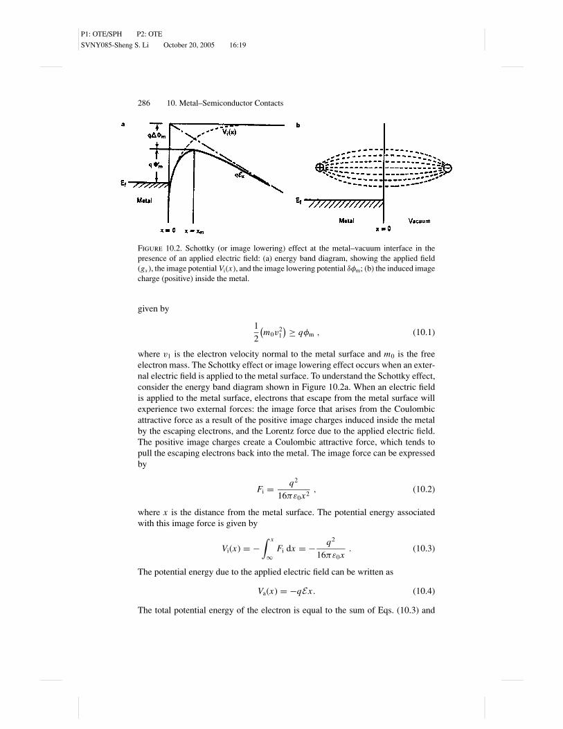
Another barrier height enhancement technique using the band gap engineeringapproach on a small band gap semiconductor such as In0.53Ga0.47As has been re-ported recently.(14) The technique involves the growth of n periods of thin gradedsuperlattices consisting of a larger band gap material and a smaller band gapepilayer of variable thickness to create a larger band gap surface layer so thatthe effective barrier height can be enhanced in such a Schottky barrier diode.For example, a high-quality In0.53Ga0.47As Schottky barrier diode has been fab-ricated by using a novel graded superlattice structure consisting of 10 periodsof n-In0.52Al0.48As/In0.53Ga0.47As graded superlattice deposited on top of the n-type In0.53Ga0.47As epilayer grown by MBE technique on the InP substrate. Theresult shows a barrier height enhancement of 0.41 eV (i.e., from φB0 = 0.3 eVto φBn = 0.71 eV), and near-ideal I–V and C–V characteristics are obtained forthis novel Schottky diode. Figure 10.26a shows the energy band diagram ofthis n-In0.52Al0.48As/In0.53Ga0.47As graded superlattice structure formed on an In-GaAs Schottky diode, and Figure 10.26b shows the dimensions of this gradedInAlAs/InGaAs superlattice layer structure and doping densities in each region.The composition of InAlAs/InGaAs and total thickness of each period remain thesame in the superlattice layer. The graded composition is achieved by changingthe thickness ratio of InAlAs/InGaAs superlattice in each period (i.e., each periodis 60 A and the thickness ratio of InAlAs/InGaAs superlattice varied from 55/5,50/10, . . . ,30/30, . . . ,5/55 A from top to the bottom layers). Figure 10.26c showsthe reverse leakage current for a Schottky barrier diode formed on the gradedsuperlattice structure shown in Figure 10.26b. It is noted that very low leakagecurrent was obtained in this InAlAs/InGaAs superlattice Schottky diode.
The third method of barrier height enhancement is to employ an MIS structure.In this approach a very thin insulating layer of a few nanometers thick is insertedbetween the metal and semiconductor to achieve barrier height enhancement. Theeffective barrier height in an MIS Schottky diode can be calculated using theexpression given by Author: The
last sentence ofthis paragraphis incomplete.Please providethe missingtext.
10.9. Applications of Schottky Diodes
Schottky diodes have been widely used for a wide variety of applications such assolar cells, photodetectors, Schottky-clamped transistors, metal gate field-effecttransistors (MESFETs), modulation-doped field-effect transistors (MODFETS orHEMTs), microwave mixers, RF attenuators, rectifiers, varactors, Zener diodes,Schottky transistor logic (STL) gate arrays, and various integrated circuits. For ex-ample, the exact logarithmic relationship displayed by the I–V curve of a Schottkydiode under forward-bias conditions over several decades of current change en-ables it to be used in the logarithmic converter circuits. A metal–semiconductorSchottky diode can also be used as a variable capacitor in parametric circuits for
P1: OTE/SPH P2: OTE
SVNY085-Sheng S. Li October 20, 2005 16:19
Figure 10.26. (a) Energy diagram of an Au/n-InAlAs/n-InGaAs Schottky barrier diodewith a 600 Å graded superlattice of InAlAs/InGaAs for barrier height enhancement, (b) di-mensions and dopant densities of the structure shown, and (c) the reverse I–V characteristicsfor this Schottky barrier diode. After Lee et al.,(14) by permission.
318

P1: OTE/SPH P2: OTE
SVNY085-Sheng S. Li October 20, 2005 16:19
10.9. Applications of Schottky Diodes 319
frequency multiplication. The Schottky barrier solar cell has the potential for use asa low-cost photovoltaic power conversion device for large-scale terrestrial powergeneration. High-speed Schottky barrier photodiodes covering a broad wavelengthrange from ultraviolet to visible and into far-IR spectral regimes have been reportedusing different metal–semiconductor materials. In this section, some practical ap-plications of Schottky barrier diodes are depicted.
10.9.1. Photodetectors and Solar Cells
A Schottky barrier diode can be used as a high-speed photodetector for low-levellight detection or as a solar cell for conversion of sun energy into electricity. Toreduce absorption loss in the metal contact of a Schottky barrier photodiode, it isa common practice to use either a thin metal film (100 A or less) or a grating-type (metal grids) structure for the Schottky contact. The reflection loss on asemiconductor surface is minimized by using an antireflection (AR) coating in thefront side of a Schottky barrier photodiode, as illustrated in Figure 10.27a. Fora grating-type Schottky barrier photodiode shown in Figure 10.27b, the patternof metal-grating structure for the Schottky contact can be defined and producedby using the photolithography technique. Selection of the metal-grid spacing isdetermined by the operating bias voltage and the substrate doping concentrationof the diode to ensure that spacing between the metal grids is fully depleted underoperating conditions. For example, in the case of an Au/n-Si Schottky diode witha doping density ND of 1014 cm−3, a spacing of around 10 µm between the metalgrids is adequate for creating a fully depleted region between the metal grids of sucha Schottky contact. A photodetector using a semitransparent Schottky contact ora grating-type Schottky contact structure has shown excellent quantum efficiencyand high responsivity.
In general, there are three detection modes that are commonly used in a Schottkybarrier photodiode; these are illustrated in Figures 10.28a, b, and c. The operationof each of these detection modes depends greatly on the incident photon energies,the applied bias voltage, and the breakdown voltage of the photodiode. These arediscussed as follows.
Figure 10.27. Schematic diagrams of (a) conventional Schottky barrier photodiode and (b)a grating-type Schottky barrier photodiode.

P1: OTE/SPH P2: OTE
SVNY085-Sheng S. Li October 20, 2005 16:19
320 10. Metal–Semiconductor Contacts
Figure 10.28. Different detection modes of a Schottky barrier photodiode: (a) qφBn ≤hν ≤ Eg, (b) hν ≥ Eg, Va � VB, (c) hν ≥ Eg, Va ∼ VB.
(i) qφBn < hv < Eg and Va � VB. In this detection mode, electrons are excitedfrom the metal and injected into the semiconductor, as illustrated in Figure 10.28.In this case, the Schottky barrier photodiode may be used for a wide variety ofapplications, which include (1) IR detector, (2) as a test structure to determinethe barrier height by the photoemission (I–E) technique, and (3) test device forstudying the bulk defects and interface states in a semiconductor, and hot elec-tron transport in a metal film. The reason that a Schottky diode can be used forlong-wavelength infrared (LWIR) detection is because the barrier height for mostSchottky diodes is smaller than the band gap energy of the semiconductor. As aresult, photons with energy equal to the barrier height absorbed inside the metalfilm of a Schottky diode usually fall in the infrared regime. Since the barrier heightfor an IR Schottky barrier photodiode is low, the reverse leakage current in such

P1: OTE/SPH P2: OTE
SVNY085-Sheng S. Li October 20, 2005 16:19
10.9. Applications of Schottky Diodes 321
a device is expected to be very large at room temperature. Therefore, in order toreduce the reverse leakage current, an IR Schottky barrier photodetector is usuallyoperated at cryogenic temperatures (e.g., T < 77 K). For example, a PtSi/p-SiSchottky barrier photodiode (with barrier height φBp = 0.2 eV) arrays integratedwith CCD (charge-couple devices) arrays have been developed for 3- to 5-µmIR image-sensor array applications. Extending the detection wavelength to 10 µmis possible if the operating temperature for the low-barrier (∼ 0.1 eV) Schottkybarrier photodiode is lowered to 4.2 K.
(ii) hv ≥ Eg and Va � VB. It is shown in Figure 10.28b that in this detectionmode, electron-hole pairs are generated inside the depletion region of the semi-conductor, and the Schottky diode may be operating as a high-speed photodetector.Since the Schottky diode is a majority carrier device, its response speed is limitedmainly by the RC time constant and the carrier transit time across the depletion re-gion of the detector. The grating-type Au/n-Si Schottky barrier photodiode shownin Figure 10.27b has a responsivity of 0.63 A/W at 0.9 µm and a bandwidth of1 GHz. The Au/n-GaAs Schottky barrier photodiode shown in Figure 10.27a has aresponse speed of less than 100 ps at 0.85 µm. In fact, a high-speed GaAs Schottkybarrier photodiode with a 3-dB bandwidth greater than 100 GHz has been reportedrecently. Further discussion of high-speed photodetectors using Schottky barrierstructures will be given in Chapter 12.
(iii) hv ≥ Eg and Va = VB. In this mode of operation, the Schottky barrier pho-todiode is in the avalanche mode of detection; this is shown in Figure 10.28c.When a Schottky diode is operating in the avalanche regime (Va = VB), an inter-nal current gain is obtained. Thus, a Schottky barrier avalanche photodiode (APD)can provide both high-speed and high-sensitivity detection. A diffused guard-ringstructure is usually employed in a Schottky barrier APD to eliminate the possibleedge breakdown effect.
A Schottky barrier photodiode can also be used as an efficient ultraviolet (UV)photon detector. For example, in the UV regime the absorption coefficient formost semiconductors is greater than 105 cm−1, which corresponds to an effec-tive absorption depth of 0.1 µm or less. Thus, by using a thin metal film andan AR coating film simultaneously on the Schottky barrier structure, efficientcollection of photons in the UV spectrum can be achieved. For example, bothAg/ZnS and Au/ZnSe Schottky barrier photodiodes have been developed forUV light detection. More recently, Schottky barrier photodiodes formed on GaNand SiC wide band gap materials have shown superior performance characteris-tics in the UV and solar blind spectral regions. This will be depicted further inChapter 12.
Finally, Schottky barrier solar cells have also been developed for photovoltaicconversion of sunlight into electricity. The Schottky barrier solar cell is easy tofabricate, and has the potential for low-cost and large-scale production. However,because of the low barrier height, Schottky barrier solar cells in general have loweropen-circuit voltage and lower conversion efficiency than most p-n junction solarcells. This will be discussed in Chapter 12.

P1: OTE/SPH P2: OTE
SVNY085-Sheng S. Li October 20, 2005 16:19
322 10. Metal–Semiconductor Contacts
Figure 10.29. A Schottky-barrier clampedbipolar transistor. The Schottky diode is con-nected between the base and collector of abipolar junction transistor.
10.9.2. Schottky-Clamped Transistors
In the saturated switching process of a conventional n-p-n or p-n-p bipolar junctiontransistor (BJT), the turnoff speed is limited by the minority carrier storage time inthe collector region of the transistor. For a Si switching transistor, the conventionalmethod of reducing the storage time is to shorten the minority carrier lifetimeby doping the Si transistors with gold impurity. However, since current gain isalso proportional to the minority carrier lifetime, the gold-doped Sil transistorwill also have a lower current gain. Therefore, it is generally not desirable todope silicon transistors with gold impurity. To overcome this problem a Schottkybarrier diode is usually added to the base–collector junction of the transistor.As shown in Figure 10.29, the minority carrier storage problem can be virtuallyeliminated if a Schottky barrier diode is connected between the base–collectorjunction of the transistor to form a Schottky-clamped transistor. The switchingtime constant is drastically shortened in this case, since the minority carrier storagein the collector is greatly reduced by the Schottky diode connecting in parallelwith the base–collector junction. In the saturation region, the collector junction ofthe transistor is slightly forward-biased instead of reverse-biased. If the forwardvoltage drop in the Schottky diode is much smaller than the base–collector voltageof the transistor, then most of the excess base current will flow through the Schottkydiode. Therefore, the minority carriers are not stored in the collector. Furthermore,the saturation time is greatly reduced when compared to a transistor without aSchottky diode connecting to the base–collector junction. A switching time ofless than 1 ns for a silicon Schottky-clamped BJT has been reported. Recently,low-power and high-speed Schottky-clamped transistor logic (STL) gate arrayshave been developed for computer and other custom IC applications. In an STLgate array, two Schottky barrier diodes with different barrier heights are used. Forexample, in the Sil STL gate array one Schottky diode (e.g., PtSi/n-Si) with largebarrier height is connected to the base–collector junction, while another Schottkydiode with low barrier height (e.g., TiW/p-Si) is connected in the collector region

P1: OTE/SPH P2: OTE
SVNY085-Sheng S. Li October 20, 2005 16:19
10.9. Applications of Schottky Diodes 323
of the transistor. The Si STL gate arrays with propagation delay times of less than1 ns and voltage swings of a few hundred millivolts or less have been achieved. TheSTL gate arrays fabricated from III-V compound semiconductors such as GaAs,InP, and InGaAs with propagation delay times of a few tens of picoseconds havealso been reported.
10.9.3. Microwave Mixers
High-frequency applications of Schottky barrier diodes deal with low-level signaldetection and mixing at microwave frequencies. It has been shown that burnoutresistance and noise performance of a Schottky diode is usually superior to that ofa point-contact mixer diode.
The frequency response of a Schottky diode is generally superior to that of ap-n junction diode, since it is limited by the RC time constant of the Schottkydiode rather than by the minority carrier lifetime as in the case of a p-n junctiondiode. Using an n-n+ epitaxial wafer for Schottky contact fabrication, both junctioncapacitance (e.g., C < 0.1 pF at Va = 0 and Nd = 1017 cm−3) and series resistanceof the diode can be reduced to a very low value. This is a direct result of usinga very thin n-type epitaxial layer on an n+-silicon substrate, and the resistancedrop across the n+ region is negligibly small. A point-contact Schottky diode withbarrier contact area of 5–10 µm in diameter has been reported. Figure 10.30 showsthe geometry of a microwave Schottky barrier diode mixer using a microstripline configuration. This Schottky diode is capable of excellent mixer performance,either as a discrete component in a waveguide or as a balanced mixer in a microstripline at carrier frequencies as high as several tens of GHz.
The RC time constant of a Schottky barrier diode can be calculated by usingan n-n+ structure with a barrier contact of radius r , which is large compared tothe epilayer thickness. The series resistance of a Schottky diode can be calculatedusing the expression
Rs = ρd
πr2=
(1
q NDµn
) (d
πr2
). (10.74)
Figure 10.30. Cross-section viewof an Au/n-type GaAs microwavemixer using a Schottky barrierstructure.

P1: OTE/SPH P2: OTE
SVNY085-Sheng S. Li October 20, 2005 16:19
324 10. Metal–Semiconductor Contacts
The depletion layer capacitance can be calculated from the expression
Cd = (πr2)
(q NDε0εs
2VD
)1/2
, (10.75)
where ND is the doping density of the n-epitaxial layer and VD is the diffusionpotential. Thus, the RC time constant for such a Schottky diode is given by
RsCd =(
d
µn
) (ε0εs
2q NDVD
)1/2
. (10.76)
To achieve high-frequency performance in a Schottky diode, the RC time con-stant of the diode must be kept as small as possible. This requires the use of a verythin epitaxial layer with high carrier mobility and doping density. Other importantapplications of the Schottky barrier structure include metal gate (i.e., Schottky gate)field-effect transistors (MESFETs) and modulation-doped field-effect transistors(MODFETs) formed on III-V compound semiconductors such as GaAs/AlGaAs,InGaAs/AlGaAs, InGaAs/InAlAs, and GaN/InGaN, and the metal–semiconductorIMPATT diodes for microwave power generation.
10.10. Ohmic Contacts in Semiconductors
Formation of good ohmic contact between metal and semiconductor is an extremelyimportant process for fabricating high-performance semiconductor devices and in-tegrated circuits. Table 10.6 gives a list of metals that are used in forming the ohmiccontacts on a wide variety of semiconductors. Good ohmic contacts are necessaryin order to effectively extract electric current and power from a semiconductor de-vice. In general, an ohmic contact is referred to a noninjecting contact in which thecurrent–voltage (I–V) relationship under both the reverse- and forward-bias condi-tions is linear and symmetrical. However, in reality, a contact is considered ohmicif the voltage drop across the metal–semiconductor interface is small compared tothe voltage-drop across the bulk semiconductor.
Ohmic contacts can be characterized in terms of the specific contact resistanceRc, which is defined as the reciprocal of the derivative of the current density withrespect to the applied voltage. An expression for the specific contact resistanceevaluated at zero bias is given by
Rc =(
dJ
dV
)−1∣∣∣∣∣V =0
. (10.77)
The specific contact resistance defined by Eq. (10.77) is an important figure ofmerit for evaluating ohmic contacts. In general, the current conduction in theohmic contact region of a metal/moderately doped n-type semiconductor contactis usually dominated by the thermionic emission process. Therefore, the expression

P1: OTE/SPH P2: OTE
SVNY085-Sheng S. Li October 20, 2005 16:19
10.10. Ohmic Contacts in Semiconductors 325
Table 10.6. Metals for forming ohmic contacts in varioussemiconductors.
Semiconductor Metals
Ge (N) Ag-Al-Sb, Al, Au, Bi, Ai-Au-P, Sb, Sn, Pb-SnGe (P) Ag-Al, Au, Cu, Ga, Ga-In, In, Al-Pd, Ni, Pt, SnSi (N) Ag-Al, Al-Au, Au, Ni, Pt, Cu, In, Ge-Sn, Au-Sb, Al-Cu,Si (P) Ag, Al, Al-Au, Au, Ni, Pt, Sn, In, Pb, Ga, Ge, Al-Cu
GaAs (N) Au-Ge (88%, 12%)-Ni, Ag-In (95%, 5%)-Ge, Ag-SnGaAs (P) Au-Zn (84%, 16%), Ag-In-Zn, Ag-ZnGaP (N) Ag-Te-Ni, Al, Au-Si, Au-Sn, In-SnGaP (P) Au-In, Au-Zn, Ga, In-Zn, Zn, Ag-Zn
GaAsP (N) Au-SnGaAsP (P) Au-Zn
GaAlAs (N) Au-Ge-NiGaAlAs (P) Au-Zn
InAs (N) Au-Ge, Au-Sn-Ni, SnInGaAs (N) Au-Ge, NiInGaAs (P) Au-Zn, Ni
InP (N) Au-Ge, In, Ni, SnInSb (N) Au-Sn, Au-In, Ni, SnInSb (P) Au-GeCdS (N) Ag, Al, Au, Au-In, Ga, In, Ga-InCdTe (N) InCdTe (P) Au, In-Ni, Pt, RhZnSe (N) In, In-Ga, Pt, In-HgSiC (N) W, NiSiC (P) Al-Si, Si, NiGaN (P) Pd-Ni, Au-NiGaN (N) Ti-Al, Ti-Al-Ni-Au
of Rc can be derived directly from Eqs. (10.33) and (10.77), which yields
Rc =(
kB
q A∗T
)exp
(qφBn
kBT
). (10.78)
Equation (10.78) shows that in order to achieve a small specific contact resistance,the barrier height of the metal–semiconductor contact should be as small as pos-sible. A smaller decrease in the barrier height will result in a very large reductionin the specific contact resistance in the Schottky contact.
For the ohmic contact on a heavily doped semiconductor, the field-emissionprocess (i.e., tunneling) dominates the current transport, and hence the specificcontact resistance Rc can be expressed by(15)
Rc ∼ exp
[(2φBn
h
) √ε0εsm∗
ND
], (10.79)
which shows that in the tunneling process, Rc depends strongly on the dopingdensity and varies exponentially with (φBn/N 1/2
D ). The specific contact resistancefor n-type GaAs may vary between 10−4 and 10−7 · cm2, while values of specificcontact resistance for GaN ranged from 10−4 to 10−8 · cm2 have been reported.

P1: OTE/SPH P2: OTE
SVNY085-Sheng S. Li October 20, 2005 16:19
326 10. Metal–Semiconductor Contacts
Figure 10.31. (a) Energy band dia-gram for a low-barrier Schottky con-tact, (b) a metal–n++–n–semiconductorohmic contact, and (c) the I–V curvefor the ohmic contact structure shownin (b).
Figures 10.31a and b show the energy band diagrams for a low barrier height contactand an ohmic contact on a heavily doped n++/n-type semiconductor, respectively.Figure 10.31c shows the I–V characteristics of a metal/n++-n-type semiconductorohmic contact. It is noted that the specific contact resistance calculated from Eq.(10.79) agrees well with the measured value for the MBE doped ohmic contacts.However, alloyed contacts usually exhibit a linear dependence of ln(Rc) on N−1/2
D ,and the simple formula given by Eq. (10.79) cannot adequately explain the I–Vbehavior of the alloyed ohmic contacts.
Formation of ohmic contacts can be achieved in a number of ways. Theseinclude (1) choosing a metal with a lower work function than that of an n-typesemiconductor (i.e., φm < φs) such that the potential barrier between the metaland the semiconductor is small enough for the thermionic emission electrons to

P1: OTE/SPH P2: OTE
SVNY085-Sheng S. Li October 20, 2005 16:19
10.10. Ohmic Contacts in Semiconductors 327
tunnel through both directions of the metal–semiconductor contact; (2) depositionof a thin and heavily doped epilayer of the same doping type as the substrate toform an n++/n or p++/p high–low junction structure on the semiconductor surface.This will reduce the barrier width of the metal–semiconductor contact such thatcurrent flow can be achieved by quantum-mechanical tunneling through the thinbarrier with low contact resistance; (3) using a graded heterojunction approach byusing a small band gap material for ohmic contact (e.g., form an n+-InAs/n-GaAsor n+Ge/n-GaAs heterojunction structure by using MBE technique); (4) using anonalloyed short-period superlattice (SPS), composed of GaN and narrow bandgap InN, sandwiched between the GaN channel and the InN cap layer to formohmic contacts on GaN; and (5) increasing the density of recombination centersat the semiconductor surface (e.g., by surface roughening) so that the surface willserve as an infinite sink for the majority carriers at the contact.
Techniques for forming ohmic contacts on the semiconductor devices includealloying, electroplating, thermal or E-beam evaporation, sputtering, ion implanta-tion, and MBE techniques. In principle, an ohmic contact is formed if the potentialbarrier between the metal and semiconductor contact is very small. It is seenin Figures 10.7c and f that in order to obtain good ohmic contact on an n-typesemiconductor, the metal work function should be less than that of the n-typesemiconductor. Conversely, to form ohmic contact on a p-type semiconductor, themetal work function must be larger than that of the p-type semiconductor. Un-fortunately, for covalent semiconductors such as Ge, Si, and GaAs, formation ofohmic contacts does not always follow the simple rule cited above. For example,the barrier height of an n-GaAs Schottky barrier contact tends to remain nearlyconstant regardless of the metals used. This is because the surface state densityfor GaAs is usually very high (e.g., ≥ 1013 cm−2 · eV−1). As a result the Fermi-level at the interface is pinned at the level where the peak interface state densityoccurs. In this case, the barrier height of the Schottky contact is determined by theFermi-level pinning at the surface and is independent of the metal work function.
The most widely used technique for forming ohmic contact on a semiconduc-tor is by first growing a heavily doped thin surface layer to form an n++/n orp++/p high–low junction structure on an n-or p-type semiconductor substrate be-fore making ohmic contact. By using such a structure, the barrier width betweenthe metal and the heavily doped n++ or p++ layer can be greatly reduced, andhence quantum-mechanical tunneling of charge carriers through such a thin bar-rier becomes possible. In this case, the barrier becomes essentially transparent tothe charge carriers, and the specific contact resistance is usually very small. Theheavily doped layer can be readily grown using alloying, thermal diffusion, ionimplantation, or epitaxial growth with a suitable dopant impurity on the growthlayer. This approach of forming ohmic contact has been quite successful for boththe silicon and GaAs IC technologies. However, it is not as successful for manylarge band gap semiconductors such as CdS, AlN, and SiC materials because thesecrystals have a tendency to compensate the foreign dopant impurities. This is dueto the large density of native defects created by the nonstoichiometric crystal struc-tures in these crystals. Finally, it should be pointed out that good ohmic contacts

P1: OTE/SPH P2: OTE
SVNY085-Sheng S. Li October 20, 2005 16:19
328 10. Metal–Semiconductor Contacts
on p-type III-V compound semiconductors are in general more difficult to achievethan their n-type counterparts. This is due to the fact that p-type III-V compoundsemiconductor surface (e.g., p-type AlGaAs) is much easier to oxidize than ann-type surface during metallization or simple exposure in the air.
Another approach that has also been employed for forming the ohmic contactson a semiconductor is introducing a large density of recombination centers at thesemiconductor surface before making ohmic contact. The recombination centersat the semiconductor surface may be created by damaging or straining the surfaceusing mechanical lapping and polishing, or by introducing impurities at the semi-conductor surface region to create large recombination centers. Plating of metalsto such a damaged surface usually results in adequate ohmic contact.
The procedures for forming ohmic contacts on a semiconductor are discussednext. Various contact-forming techniques, such as alloying, thermal or E-beamevaporation, sputtering, ion implantation, plating, and liquid regrowth have beenemployed. The alloying process can be achieved by first placing the metal pelletsor a thin metal foil on the semiconductor surface and then heating the specimen tothe eutectic temperature of metal such that a small portion of the semiconductor isdissolved with the metal. The contact is then cooled, and semiconductor regrowthtakes place. This regrowth results in the incorporation of some metal and resid-ual impurities into the metal–semiconductor interface. In this method, impuritiesin the metal form a heavily doped interfacial layer of the same dopant type asthe bulk semiconductor, and hence good ohmic contact on the semiconductor canbe obtained. However, many large band gap semiconductors have contact prob-lems because they cannot be doped heavily enough to form good ohmic contact.Another technique for making ohmic contact is to wet the semiconductor with ametal. In order to promote wetting and good ohmic contact, both the metal andsemiconductor surface must be ultraclean. A flux is often used during alloying inorder to remove any residual impurities or oxide film such that surface wetting canbe enhanced. Care must be taken to identify the difference in thermal expansioncoefficients between the semiconductor and metal so that residual stress does notdevelop in the semiconductor upon cooling from the alloying temperature to roomtemperature. Liquid regrowth can also be used to form a high–low junction (i.e.,n+/n or p+/p) on a semiconductor substrate before forming ohmic contact. Thistechnique has been used to form ohmic contact on GaAs Gunn-effect devices.
Ohmic contacts on semiconductors can also be achieved by using electrodelessplating. This method involves the use of a metallic salt (such as AuCl3), whichis reduced to a metal at the semiconductor surface by a chemical reducing agentpresent in the plating solution. Solutions of nickel, gold, and platinum are the mostwidely used metals for electrodeless plating in semiconductors. It has been foundthat a nickel film adheres better on a mechanically lapped semiconductor surfacethan on a chemically polished semiconductor surface.
In the traditional silicon IC technology, the most commonly used techniquefor depositing metal films on silicon devices in IC chips is by using thermal orelectron-beam (E-beam) evaporation. The E-beam evaporation is particularly at-tractive for integrated circuits in which complex contact patterns are formed byusing a photolithography technique. The metal contact is deposited by using a

P1: OTE/SPH P2: OTE
SVNY085-Sheng S. Li October 20, 2005 16:19
10.10. Ohmic Contacts in Semiconductors 329
heated filament, an E-beam gun, or by using sputtering. The heated boat or fila-ment technique is the simplest method, but suffers from the disadvantage of beingcontaminated by the heated container (e.g., tungsten basket or graphite boat). Ashutter mechanism is often used to block the initial vapor that may be contaminatedwith the more volatile impurities. If multiple boats or filaments are used, two ormore metals may be evaporated simultaneously with independent control of eachevaporating source. In the E-beam system, the E-beam gun melts the evaporantalone, which serves as its own crucible. This eliminates contamination from thecrucible and gives purer deposited metal films. In the sputtering system, positivegas ions bombard the source (cathode), emitting metal atoms. These ejected atomstraverse the vacuum chamber and are deposited onto the semiconductor substrate.The sputtering system has the advantage that the polarity of the system may bereversed so that sputtering may occur from the substrate to a remote anode, therebycleaning the substrate surface. The back-sputtering approach is particularly usefulfor removing any residual thin oxide films or other impurities on the substratesurface while it is in the vacuum, and can be followed immediately by depositingmetal contact on the substrate.
The standard procedure for making ohmic contacts in silicon IC fabrication isusually accomplished by a two-step process. In general, ion implantation is firstemployed to create a thin, heavily doped layer of the same dopant type as that ofthe bulk material to form a p+/p or n+/n high–low junction, and is then followed bydeposition of metal contacts using either thermal or E-beam evaporation. Finally,thermal annealing is performed on the implanted region to achieve good ohmiccontact. In this procedure, careful cleaning of the semiconductor surface is essentialto ensure good ohmic contact prior to metal deposition.
The wire bonding in semiconductor devices is usually carried out using either thethermal compression or ultrasonic wire bonder. In thermal compression bonding,both heat and pressure are applied simultaneously to the ball bonder (using 1-milgold or aluminum wires) and the contact pad. In ultrasonic bonding, a combinationof pressure and 60 kHz ultrasonic vibrations is employed. The ultrasonic vibrationgives rise to a scrubbing action that breaks up any thin surface insulating film,and hence intimate contacts between the metal and semiconductor can be made.The advantage of using ultrasonic bonding is that heating is not required, and anyprevious bondings will not be affected.
In conventional silicon IC technologies, interconnects are incorporated afterfront-end processing. The front-end processing refers to the sequence of fabri-cation steps, typically at very high temperatures (700–1100◦C), that form theMOS transistors in the active regions, the pockets of thick isolation in the fieldregions that separate adjacent transistors, and the silicidation of the transistor ter-minals for low-resistance contacts. The back-end processing, which refers to theinterconnection of transistors, is subsequently formed by contacting the transistorterminals and then vertically stacking layers of metal wires and vias encased inthe dielectric materials. Backend processing temperatures typically do not exceed450◦C to avoid melting of metals and to control stress. Integration success in theconventional silicon IC technology is largely attributed to the processes that main-tain excellent planarity after fabricating each and every via and wire level. The

P1: OTE/SPH P2: OTE
SVNY085-Sheng S. Li October 20, 2005 16:19
330 10. Metal–Semiconductor Contacts
state-of-the-art 0.25-µm backend processing uses the integration of conventionalAl metallization and Al alloy (Al/Cu) wires and W vias (plugs or studs), whichserves as a blocking barrier to the Al for diffusing into silicon transistors andoxides.
In 1999, IBM Corp. introduced a new chip manufacturing technique to themainstream to boost the performance of Power PC microprocessor by more than30% using a combination of the SOI (silicon-on-insulator) technology and thecopper-interconnect wiring scheme. The high-performance copper-interconnectstechnique offers lower contact resistance to the transistors, lower wiring parasiticcapacitance, and significantly higher electromigration resistance over the standardAl or Al alloy interconnnects. It improves the overall chip performance includinghigher speed, higher packing density, and lower power consumption for the mi-croprocessor. In silicon IC industry, the method of embedding metal structures indielectrics (known as the Damascene process) is widely used for metal wire inter-connects. The copper interconnects are usually deposited using electrochemicalplating instead of the physical vapor deposition (PVD) process. Since the PVDprocess could not fill the Damascene features, and is more expensive than theelectroplating technique, tungsten (W) via (plug) technology has matured to thepoint where void-free and untapered vias with aggressive aspect ratios exceeding3:1 are routinely formed, thus enabling increases in wiring density and reductionof capacitive parasitics to under- and overlying wires. Advances in lithographyalignment have also enabled borderless vias to be formed, thereby permitting evenfurther improvement in wiring density. In addition, Damascence tungsten has beenadapted as planar local interconnects for strapping source/drain and gate contacts.Although this process is more difficult to control, successful implementation ofW-local interconnects can reduce the cell size of SRAMs used as microprocessorcache memories by 20–30%.
Problems
10.1. The saturation current density for a thoriated tungsten metal is 1 A/cm2 at1873 K, and the work function computed from Eq. (10.11) for this metalis 3.2 eV. Assume that A0 = 120 A/cm2 · K2.(a) Plot ln(J ′
s ) versusE1/2 for T = 1873 K and for 104 < E1/2 < 107 V/cm.(b) Repeat (a) for T = 873 K and 1500 K.
10.2. (a) Draw the energy band diagram for an ideal metal/p-type semiconductorSchottky barrier diode and show that the barrier height for a metal/p-type semiconductor is given by Eq. (10.14).
(b) Plot the energy band diagrams for an ideal metal/p-type semiconductorSchottky barrier diode for
(i) φm > φs.(ii) φm < φs.
(iii) Explain which of the above cases would yield an ohmic or a Schot-tky contact.

P1: OTE/SPH P2: OTE
SVNY085-Sheng S. Li October 20, 2005 16:19
10.10. Ohmic Contacts in Semiconductors 331
10.3. Using Eq. (10.25), plot the depletion layer width versus reverse-biasvoltage (VR = 0 to 20 V) for an Au/n-type silicon Schottky barrierdiode for ND = 1014, 1016, and 1018 cm−3. Given εs = 11.7, VD = φBn −(kBT/q), ln(NC/ND), and qφBn = 0.81 eV at T = 300 K.
10.4. Taking into account the image lowering effect by using Eq. (10.34), plotthe saturation current density versus reverse-bias voltage for an Au/n-Siand Pt/n-Si Schottky diode. Assume that qφBn = 0.81 eV for an Au/n-SiSchottky diode, qφBn = 0.90 eV for a Pt/n-Si Schottky diode, and A∗ =110 A/cm2 · K2.
10.5. Derive Eqs. (10.30) and (10.42), and compare the results with the currentdensity equation derived from the thermionic–diffusion model by C. R.Crowell and S. M. Sze.(1)
10.6. Design an Au/n-type GaAs Schottky barrier photodiode for detecting a 20-GHz modulated optical signal with center wavelength at 0.84 µm. Showthe Schottky barrier structure, and calculate the thickness of the AR coatinglayer (e.g., SiO2), the diode area, and the RC time constant of this pho-todiode. If the incident photosignal has a power intensity of 2 mW/cm2,what is the responsivity of this photodiode? (Hint: Choose your own designparameters.)
10.7. If the barrier height of a TiW/p-type Si Schottky barrier diode is equal to0.55 eV, use Eqs. (10.65) and (10.66) and Eqs. (69) through (73) to design aTiW/n+-p Schottky barrier diode structure to enhance the effective barrierheight to 0.90 eV. Assuming that the p substrate has a dopant density of1 × 1016 cm−3, calculate the required dopant density and thickness of then+ surface layer.
10.8. Assuming that the diode ideality factor n for a Schottky barrier diode isdefined by
n =(
q
kBT
)∂V
∂(ln J ),
(a) Show that
n ={
1 +(
∂�φ
∂V
)+
(kBT
q
) [∂(ln A∗)
∂V
]}−1
.
(b) What are the possible physical mechanisms that may cause the n valueto deviate from unity?
10.9. Using the general expressions of the barrier height for a Schottky barrierdiode given by Eqs. (10.48) and Eqs. (10.49) to (10.51), with Ds
∼= 1.1 ×10¹³(1 − c2)/c2 states/cm2-eV, where Ds is the interface state density,(a) What is the barrier height if Ds is approaching to infinity? Explain the
Fermi-level pinning effect under this condition.(b) If Ds → 0, what is the value of c2 and the expression for φBn?

P1: OTE/SPH P2: OTE
SVNY085-Sheng S. Li October 20, 2005 16:19
332 10. Metal–Semiconductor Contacts
(c) If the values of c2, c3, and χs for Si, GaAs, and GaP Schottky contactsare given by:
c2 = 0.27, 0.09, and 0.27 for Si, GaAs, and GaP, respectively,c3 = −0.66, −0.61, and
−0.07V for Si, GaAs, and GaP, respectively,χs = 4.05, 4.07, and 4.0 V for Si, GaAs, and GaP, respectively,
calculate the values of Ds, qφ0, and qφBn for the above Schottky diodes.10.10. Using Eqs. (10.69) to (10.73), calculate the barrier height enhancement for
an Au/p-n GaAs Schottky barrier diode for the following cases:(a) Nd = 1016 cm−3, plot φBn versus Na(1015 to 5 × 1018 cm−3) for
Wp = 0.3, 0.2, 0.1, 0.05, and 0.02 µm; qφBn = 0.9 eV for an Au/n-GaAs Schottky contact.
(b) Na = 2 × 1017 cm−3, calculate and plot φBn versus Nd and Wn for thevalues given in (a).
References
1. C. R. Crowell and S. M. Sze, Solid-State Electron. 8, 979 (1966).2. A. Y. C. Yu and C. A. Mead, Solid-State Electron. 13, 97 (1970).3. D. Kahng, Bell Syst. Tech. J. 43, 215 (1964).4. M. P. Lepselter and S. M. Sze, Bell Syst. Tech. J. 47, 195 (1968).5. A. M. Cowley and S. M. Sze, J. Appl. Phys. 36, 3212 (1965).6. R. H. Fowler, Phys. Rev. 38, 45 (1931).7. C. R. Crowell, J. C. Sarace, and S. M. Sze, Trans. Metall. Soc. AIME 233, 478 (1965).8. E. Hokelek and G. Y. Robinson, J. Appl. Phys. 54(9), 5199 (1983).9. W. Schottky, Naturwissenschoften 26, 843 (1938).
10. J. Bardeen, Phys. Rev., 71,171 (1947).11. K. A. Rickert, A. B. Ellis, J. K. Kim, J. Lee, F. J. Himpsel, F. Dwikusuma, and T. F.
Kuech, J. Appl. Phys. 92, 6671 (2002).12. S. S. Li, Solid-State Electron. 21, 435–438 (1977).13. S. S. Li, C. S. Kim, and K. L. Wang, IEEE Trans. Electron Devices ED-27, 1310–1312
(1980).14. D. H. Lee, S. S. Li, N. J. Sauer, and T. Y. Chang, Appl. Phys. Lett. 54(19), 1863 (1989).
Author: Pleasecite Refs. 16–19in the text.
15. F. A. Padovani and R. Stratton, Solid-State Electron. 9, 695 (1966).16. A. R. Vearey-Roberts and D. A. Evans, Appl. Phys. Lett. 86 (7), (Feb. 14 2005).Author: Please
provide pagerange.
17. A. Haluk, Appl. Surf. Sci. 242 (3/4), 412 (2005).18. Tredgold et al., J. Appl. Phys. 103–109 (Jan.14 1985).
Author:Pleaseprovide thenames of allauthors withtheir initials.Also providethe vol. no.
19. C. Y. Wu, J. Appl. Phys. 51(7), 3786 (1980).
Bibliography
E. H. Rhoderick and R. H. William, Metal–Semiconductor Contacts, Vol. 19, 2nd ed.,Oxford University Press, Oxford (1988).
N. Braslau, Thin Solid Films 104, 391 (1983).P. Chattopadhyay and A. N. Daw, Solid-State Electron. 28, 831 (1985).M. Heiblum, M. I. Nathan, and C. A. Chang, Solid-State Electron. 25, 185 (1982).

P1: OTE/SPH P2: OTE
SVNY085-Sheng S. Li October 20, 2005 16:19
10.10. Ohmic Contacts in Semiconductors 333
H. K. Henisch, Semiconductor Contacts: An Approach to Ideas and Models, ClarendonPress, Oxford (1984).
V. G. Keramidas, Inst. Phys. Conf. Ser. No. 45, 396 (1979).R. S. Muller and T. I. Kamins, Device Electronics for Integrated Circuits, Wiley, New York
(1977).A. Piotrowska et al., Solid-State Electron. 26, 179 (1983). Author: Please
provide thenames of all theauthors.
E. H. Rhoderick, Metal–Semiconductor Contacts, Clarendon Press, Oxford (1978).V. L. Rideout, Solid-State Electron. 18, 541 (1975).B. L. Sharma, in: Semiconductors and Semimetals, Vol. 15, Academic Press, New York
(1981), p. 1.B. L. Sharma, Metal–Semiconductor Schottky Barrier Junctions and Their Applications,
Plenum Press, New York (1984).W. E. Spicer, P. W. Chyre, C. M. Garner, I. Lindau, and P. Pianetta, Surf. Sci. 86, 763 (1979).W. E. Spicer, I. Lindau, P. Skeath, C. Y. Su, and P. W. Chyre, Phys. Rev. Lett. 44, 420 (1980).S. M. Sze, Physics of Semiconductor Devices, 2nd ed., Wiley, New York (1982).A. Van der Ziel, Solid State Physical Electronics, 3rd ed., Prentice Hall, New York (1976).C. W. Wilmsen, Physics and Chemistry of III-V Compound Semiconductor Interfaces,
Plenum Press, New York (1985).D. A. Neamen, Semiconductor Physics and Devices, McGraw-Hill Publishing, New York
(2003).


![Influence of Metal–Graphene Contact on the Operation and ......metal-induced gap states in conventional metal–semiconductor contacts [25]. Experiments have also confirmed that](https://static.fdocuments.in/doc/165x107/5f9826031cd51e799d443f86/iniuence-of-metalagraphene-contact-on-the-operation-and-metal-induced.jpg)