
![Dist-GAN: AnImproved GAN using Distance Constraints...Dist-GAN: AnImproved GAN using Distance Constraints Ngoc-Trung Tran[0000−0002−1308−9142], Tuan-Anh Bui[0000−0003−4123−262],](https://static.fdocuments.in/doc/165x107/60aad22afa8ec440d64b3f4c/dist-gan-animproved-gan-using-distance-constraints-dist-gan-animproved-gan.jpg)


Languages
Pages
Legal


WHITEPAPER
See, Feel, and Hear the Difference with GaNClass-D Amplifier and Companion SMPS
LEARN MORE AT GANSYSTEMS.COM

Table of Contents
3
4
5
6
12
16
17
Introduction
Amplifier and SMPS designs
Performance Test and Validation
Performance Characterization Results
Efficiency and Thermal Performance Results
Benefits of GaN-based Class-D Audio Hardware
Summary

IntroductionAs engineers within the design community read and learn about new products and topologies,
they become skeptical about the promises for improved operating characteristics. The promise of
a step-function improvement with GaN in audio systems could be classified as one of these
scenarios. However, with the GaN Systems Stereo Class-D Amplifier system solution, the audio
industry is pleasantly surprised to see that GaN is keeping its promise.
The GaN Systems solution consists of a GaN FET-based LLC SMPS with PFC and Stereo
200W/8-ohm Class-D Amplifier. The SMPS uses the GaN Systems GS66506T for both PFC
Front-End and LLC Half-Bridge Back-End and the GaN Systems GS61008P for each of the four
Half-Bridge Output Stages of the Class-D Amplifier.
This whitepaper reviews the GaN Systems audio evaluation kit using the standard set of industry
performance and validation tests. These tests include, but were not limited to:
• Performance Specification Testing – Power Output and Efficiency
• Performance Characterization Testing – THD vs Power, Frequency; Frequency Response; Noise Floor
• Efficiency and Thermal Performance Testing – Amplifier and SMPS
• Amplifier Robustness Testing – 4-ohm, 8-ohm Performance; 200W into 8 ohms, 300W into 4 ohms; Current-Limit Functionality
• Amplifier Sonic Quality Testing - Listening Test, Sonic Quality Assessment
See, Feel, and Hear the Difference with GaN Class-D Amplifier and Companion SMPS Design
- 3 -

Amplifier and SMPS designsThe Class-D Amplifier is a two-channel Bridge-Tied-Load (BTL) design, composed of four
ground-referenced Half-Bridge Output Stages with evident support for scalability and
expandability. The design of the companion SMPS is a high-efficiency LLC design with PFC and
Universal Input support. These architectures and topologies are the most scalable. The Amplifier
and SMPS platforms are also readily modified to a wide variety of cost-effective Controllers.
AMPLIFIER DESIGNThe user guide for the Class-D evaluation kit shows the following specifications.
Power Output 200Wrms into an 8-ohm load
300Wrms into a 4-ohm load
THD+N (open loop) < 0.2% into an 8-ohm load, 1kHz
< 0.3% into a 4-ohm load, 1kHz
THD+N (closed loop) < 0.02% into an 8-ohm load, 1kHz
< 0.03% into a 4-ohm load, 1kHz
SNR > 115dB (open loop)
> 105dB (closed loop)
Frequency Response 20Hz to 20kHz, +/- 0.5dB, 6-ohm
Switching Frequency 400kHz (closed loop)
384kHz (open loop)
Efficiency > 95%
Power Supply Voltage < +/- 32VDC for 2x BTL and Ground-Referenced Output
The Amplifier provides the following interfaces which support the application and evaluation
requirements.
Input/Source
Analog 3.5mm Stereo Mini-Plug
Single-ended RCA Phono x 2, Unbalanced, 1Vrms
Digital Coaxial Digital (S/PDIF)
Optical Digital (S/PDIF)
Volume Control Encoder Digital – On Board
Power Supply input 6-Pin JST Latching Connector (+HV, -HV, Ground)
Output Power 4-Pin Phoenix Connector x 2 (+L, -L, +R, -R)
See, Feel, and Hear the Difference with GaN Class-D Amplifier and Companion SMPS Design
- 4 -
SMPS DESIGNThe SMPS design includes an existing and proven high-efficiency LLC architecture and
universal PFC input with the following specifications.
AC Voltage Input 85VAC to 265VAC
50Hz/60Hz
DC Output +/- 32VDC @ 12A
The SMPS platform provides the following connectivity.
Input Power 5-Pin JST Latching Connector (Line, Neutral, Ground)
Output Power 6-pin JST Latching Connector (+HV, -HV, Ground)
See, Feel, and Hear the Difference with GaN Class-D Amplifier and Companion SMPS Design
- 5 -

See, Feel, and Hear the Difference with GaN Class-D Amplifier and Companion SMPS Design
- 6 -
Performance Test and ValidationThe GaN Systems Class-D evaluation kit is tested and validated using industry-standard
measurements with recognized techniques and equipment. The Test Bench utilizes the following
equipment for bring-up, test, and evaluation:
• Tektronix DPO3034 Digital Oscilloscope (or equivalent)
• Audio Precision AP2700 System Two Cascade or APx555B w/Switcher & AES-17 Filter
The standard set of industry performance and validation tests were run using this Test
Bench. These tests include, but were not limited to:
Performance Specification Testing
Power Output (200W into 8 ohms)
Power Output (300W into 4 ohms)
Efficiency
Performance Characterization Testing
THD+N vs. Power/Level
THD+N vs. Frequency
Frequency Response (8-ohm, 4-ohm)
Limited by Audio Precision AES-17 Brick-Wall Filter
Noise Floor (SNR)
Efficiency and Thermal Performance Testing
Amplifier Efficiency Measurements
SMPS Thermal Performance
Amplifier Robustness Testing
4-ohm, 8-ohm Performance
200W into 8 ohms
300W into 4 ohms
Current-Limit Functionality
Amplifier Sonic Quality Testing
Listening Test/Sonic Quality Assessment
See, Feel, and Hear the Difference with GaN Class-D Amplifier and Companion SMPS Design
- 7 -
Performance Characterization ResultsThe system characterization was performed on the complete Class-D Amplifier/SMPS evaluation
platform combination. To follow are the results of both the initial Characterization and the
Thermal Performance measurements that were performed on the GaN FET Class-D Amplifier
platform. Unless otherwise noted, the Characterization was performed with the companion GaN
Systems GaN FET LLC SMPS that allow for the specification of 200W/8-ohms and 300W/4-ohms.
This requirement resulted in Power Supply Voltage rails of +/-32VDC. The companion GaN
Systems LLC Power Supply provides up to 350W of clean power into 8 ohms. This Power Supply
was only altered in the Thermal Performance testing to allow for a more exact comparison with
other Class-D Amplifier Platforms.
This reference design accommodates both Open-Loop and Closed-Loop operation. Many Class D
amplifiers in the market utilize negative feedback from the PWM output back to the input of the
device. These Class D amplifiers typically use silicon MOSFETs which cause non-linearities in the
system. A closed-loop approach not only improves linearity, but also allows the system to have
power supply rejection. This contrasts with an open-loop amplifier, which inherently has minimal
(if any) supply rejection. Because the output waveform is sensed and fed back to the input of the
amplifier in a closed-loop topology, deviations in the supply rail are detected at the output and
corrected by the control loop. The advantages of a closed-loop design come at the price of
possible stability issues as is the case with all systems utilizing feedback.
GaN FETs have changed the paradigm. No longer do the assumptions above need to apply to
amplifier design. In the following figures, measurements with the system in both open-loop and
closed-loop are measured. From the THD+N vs. Power plot (Figure 1), it can be readily determined
that the low signal level THD performance for the Open-Loop amplifier exceeds that of the
Closed-Loop approach.
This is mainly due to the increase Noise contribution of the feedback and can easily be
understood by comparing this data to the Noise Floor performance illustrated below in Figure 3.
As the audio signal level is increased, and hence the output power increased, the benefit of the
Closed-Loop architecture is evident. However, the THD+N of the Open-Loop architecture
compares very favorably, mainly due to the excellent switch characteristics of the GaN Systems
transistors in the output stage.

See, Feel, and Hear the Difference with GaN Class-D Amplifier and Companion SMPS Design
- 8 -
By using an Open-Loop architecture with the ability to tightly control the switching deadtime,
near Closed-Loop THD performance can be achieved. This is apparent in the THD+N vs. Frequency
figures below as well. The increase in THD+N with the Open-Loop architecture, and at the lower
frequencies is mainly due to the lack of Power Supply Rejection, and the contribution to the
system-level performance by the SMPS. However, as with the THD+N vs. Power measurements,
the Open-Loop architecture very quickly approaches the performance of the Closed-Loop
architecture in the upper-mid-range.
The THD vs. Level performance capture in Figure 1 indicates both Open-Loop and Closed-
Loop results for a 1kHz Sine Wave and an 8-ohm, non-inductive load.
Figure 1: THD+N vs. Power (Level) into 8 Ohms @ +/-32VDC

See, Feel, and Hear the Difference with GaN Class-D Amplifier and Companion SMPS Design
- 9 -
Figure 2: THD+N vs. Frequency into 8 Ohms @ -9dBFS
Figure 2 illustrates the THD+N vs. Frequency at a measurement level of -9dBFS – once again into
an 8-ohm, non-inductive load. Both Open-Loop and Closed-Loop performances are captured
under the same SMPS measurement conditions.

See, Feel, and Hear the Difference with GaN Class-D Amplifier and Companion SMPS Design
- 10 -
Figure 3: Noise Floor Relative to 0dBFS
Figure 3 provides a capture of the Noise Floor for both Open-Loop and Closed-Loop
configurations.

See, Feel, and Hear the Difference with GaN Class-D Amplifier and Companion SMPS Design
- 11 -
Figure 4: Frequency Response into an 8-ohm Load @ -9dBFS
Figure 4 provides a capture of the Frequency Response of the GaN Systems Class-D Amplifier into
an 8-ohm load.
The slight peaking in the response is due to the alignment of the Output L/C Reconstruction
Filter. In this design, to allow the best trade-off between both 8-ohm and 4-ohm loads, the Output
Filter is optimized for a 6-ohm load. This optimization results in this small peak in the Frequency
Response for an 8-ohm load, and a corresponding mild roll-off into a 4-ohm load.

See, Feel, and Hear the Difference with GaN Class-D Amplifier and Companion SMPS Design
- 12 -
Figure 5: Class-D Amplifier FFT With and Without Input Signal @ -60dBFS
To illustrate the content of the measured Noise contribution for the above plots, Figure 5 provides
a snapshot of the Fast Fourier Transform (FFT), both with and without Audio Input Signal.
Efficiency and Thermal PerformanceThe Efficiency and Thermal Performance characterization was performed on the complete
Class-D Amplifier/SMPS Demonstration platform combination and on the individual PCBAs to
assure the best capture of performance.
To capture correct and accurate efficiency measurements, it is first necessary to characterize the
‘idle’ current/power usage of the entire Amplifier, since most of this ‘idle’ dissipation is not
associated with the GaN FET Amplifier Power Stage, but is associated with the other peripheral
circuitry on the Amplifier PCBA. This ‘idle’ current requirement is usually reflected in a significant
reduction in efficiency as the output power level is reduced to the point where this ‘idle’
dissipation becomes an appreciable percentage of the overall dissipation. This resultant “Idle
Dissipation” was captured to assure an accurate measurement of amplifier efficiency.

See, Feel, and Hear the Difference with GaN Class-D Amplifier and Companion SMPS Design
- 13 -
Figure 6: Closed-Loop Amplifier Efficiency vs. Output Power @ 8 Ohms
Figure 7: Open-Loop Amplifier Efficiency vs. Output Power @ 8 Ohms
In Figure 6 and Figure 7, the blue line is this “Idle Dissipation” which was subtracted from the
overall dissipation. This is the appropriate approach, as this “Idle Dissipation” does not factor into
the “Efficiency” of the GaN FET Power Stage. It also does not prove to be a significant contributor
to the overall efficiency at the power levels which would create the need for costly components
such as heat sinks and large copper mounting tabs. For comparison purposes, the red plot line of
Figure 6 and Figure 7 adds back the additional power loss that is characteristic of the total Class-D
Amplifier Test Platform, but does not include the peripheral dissipation associated with
components that are not a part of the Amplifier Platform.

See, Feel, and Hear the Difference with GaN Class-D Amplifier and Companion SMPS Design
- 14 -
Hence, the blue curve in each plot indicates the efficiency of the Power Stage and should be used
when comparing the GaN FET Efficiency with other MOSFET or Integrated Power Device
solutions. The red curve in each plot indicates the efficiency of the GaN-based Class-D Amplifier
and should be used in comparison with other complete MOSFET Reference Designs (that are
measured equivalently) or Integrated Power Amplifiers (with equivalent Power Output
capability).
“Blue” Curve (Heat Sink consideration): With the 8-ohm Power Stage Efficiency, measured at 95%
to 96% efficient, this places the GaN FET Power Stage at 6% - 10% higher than a similar MOSFET
Class-D Power Stage of the same Power Output capability. For compact system solutions, this
increase in efficiency allows for the complete removal of any classical or historical heat sink
requirement. This elimination of the heat sink also reduces the potential contribution to radiated
EMI/EMC emissions. These two combined characteristics make the GaN FET Class-D Amplifier a
very desirable alternative to the incumbent MOSFET Class-D Amplifier architectures.
“Red” Curve (Power Supply consideration): With the 8-ohm Amplifier efficiency measured at 90%
to 96% efficient, this places the GaN FET Amplifier from 3% - 10% higher than a similar MOSFET
Class-D Amplifier of the same Power Output capability. An additional item of interest is that the
category of Integrated Power Amplifier could NOT play in the 8-ohm application that is defined
by this performance.
Since the companion SMPS is also based on GaN Systems devices, it is also desirable to consider
the increase efficiency and resulting cost reduction of this application. One of the driving factors
in this particular design is the desire for reduced size and complexity, even at the potential
sacrifice of some amount of efficiency. Other topologies are available for both the PFC
implementation and the LLC implementation. However, for this Class-D Amplifier SMPS targeted
performance, the additional complexity was not warranted.
A simple, single GaN FET design was used for the Front-End PFC, and a simple, dual-GaN FET
Half-Bridge was used for the Back-End LLC. This allows for a very low cost, 3-FET design that does
not need any massive external heat sink for full-power operation. As an illustration of the
Operating Temperature of the SMPS under the Load conditions, the following Thermal Data was
captured.
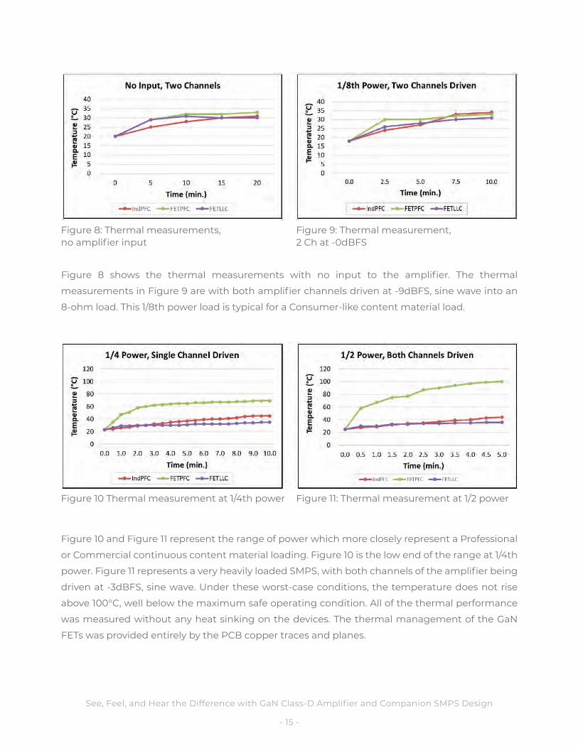
Figures 8 through 11 capture the thermal performance of the GaN Systems SMPS design under
varying amplifier load conditions, all continuous sine wave driven. These figures show the
temperature of the PFC Inductor (IndPFC), PFC GaN FET (FETPFC) and LLC Half-Bridge GaN FET
(FETLLC).
See, Feel, and Hear the Difference with GaN Class-D Amplifier and Companion SMPS Design
- 15 -
Figure 8: Thermal measurements, no amplifier input
Figure 9: Thermal measurement, 2 Ch at -0dBFS
Figure 10 Thermal measurement at 1/4th power Figure 11: Thermal measurement at 1/2 power
Figure 8 shows the thermal measurements with no input to the amplifier. The thermal
measurements in Figure 9 are with both amplifier channels driven at -9dBFS, sine wave into an
8-ohm load. This 1/8th power load is typical for a Consumer-like content material load.
Figure 10 and Figure 11 represent the range of power which more closely represent a Professional
or Commercial continuous content material loading. Figure 10 is the low end of the range at 1/4th
power. Figure 11 represents a very heavily loaded SMPS, with both channels of the amplifier being
driven at -3dBFS, sine wave. Under these worst-case conditions, the temperature does not rise
above 100°C, well below the maximum safe operating condition. All of the thermal performance
was measured without any heat sinking on the devices. The thermal management of the GaN
FETs was provided entirely by the PCB copper traces and planes.

See, Feel, and Hear the Difference with GaN Class-D Amplifier and Companion SMPS Design
- 16 -
Benefits of GaN-based Class-D Audio HardwareWhen it comes to implementing the best sounding, most efficient Class-D audio hardware, the
most compelling transistor switching platform choice is GaN Systems power transistors. In this
audio reference design evaluation kit from GaN Systems, the system features:
AUDIO AMPLIFIER
The GaN Systems design with GaN FETs provides the right combination of performance, size, and
power consumption for Class-D audio applications. With the selected design topology and
resulting thermal and sonic performance, the design is scalable in many ways. Derivative designs
include: increasing power by using a heatsink on the GaN Systems top-side cooled devices or
tying the two outputs together, or reducing power by going to half bridge without BTL or a single
rail design.
Complete Class-D Amplifier
• Multi Audio Signal Inputs
• Bridge-Tied Load Output
• On-Board Power Management
High-Performance Audio
• 200W/Ch (8Ω), 300W/Ch (4Ω)
• > 108dB SNR & Dynamic Range
• < 0.01% THD+N (8Ω, 1W)
• +/- 0.5dB Freq. Response (8Ω)
High-Performance Output
• 96% Efficiency
• Reduced thermals
Complete Audio LLC SMPS
• Universal AC Line Input
• Easy Integration w/GaN Amplifier
• Common-Mode AC Filter
High-Performance Audio
• 400W Continuous, 550W Peak
• +/-32VDC Dual-Rail Output
High-Performance Output
• No heatsinking, no cooling
• High efficiency, 40% loss decrease
• EMI/EMC friendly

LEARN MORE AT GANSYSTEMS.COM
SummaryThe measurements indicate that the performance
of this reference design is very good and system
designers now have a choice between Open-Loop and
Closed-Loop designs. The use of good Open-Loop topologies
allows for the elimination of complexities associated with a
Closed-Loop design counterpart. Additionally, the Open-Loop topology
allows for both “static” and “real-time” optimization of audio performance
vs. EMI/EMC profile vs. thermal performance. Lastly, for the Open-Loop design,
the Power Supply becomes an even more important component in the overall
audio system solution and the companion SMPS in this evaluation kit is a good pairing
with the amplifier.
Audio quality has become an important part of nearly every interaction people
have today. Ranging from your phone to your car to your home, everyone
wants good sound quality and can have it. No longer is good sound only
affordable for the audiophiles, expensive cars, or elaborate home sound
systems. GaN devices provide the performance, size, and cost benefits
to allow everyone to enjoy Class-D audio sound.
Visit Our Website:
Download Evaluation Kits >
Find Out Where to Buy >
Contact Us >
Top Related