
Applications for GaN Power...
22
1 Applications for GaN Power Semiconductors Eric Persson GaN Applications & Marketing October 2014
Transcript of Applications for GaN Power...

1
Applications for GaN
Power Semiconductors
Eric Persson
GaN Applications & Marketing
October 2014

Why GaN for Power Electronics?
Today’s Silicon Options for 600 V Switch:
SuperJunction FET (CoolMOS, MDMesh)
• Pro: Low Rds(on) per area; reasonable cost
• Con: Very poor body diode; nonlinear Qoss
• Typical applications: Power Supplies
Traditional Planar FET (FREDFET)
• Pro: low cost process; performance similar to superjunction
• Con: large die area for a given Rds(on)
• Typical applications: Legacy power supplies
IGBT (with co-packaged diode)
• Pro: Very low $/A; short-circuit capable
• Con: High Vce(on); no sync rect; switching loss limits freq.
• Typical applications: Motor drives, UPS inverters
2
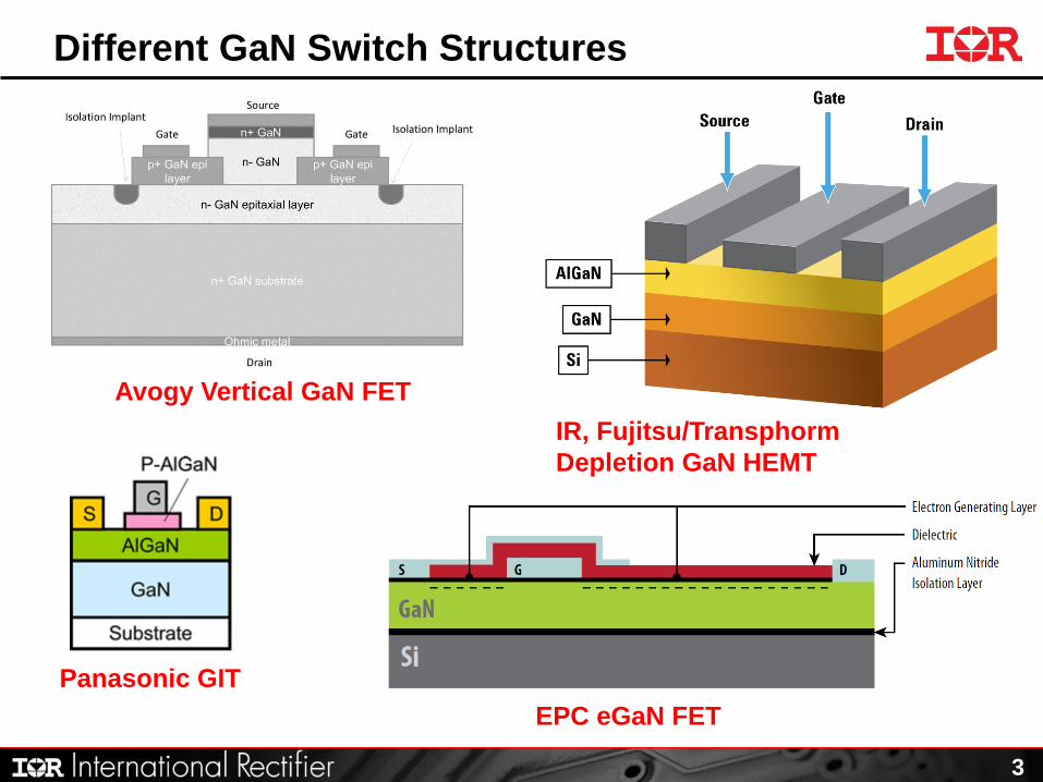
Different GaN Switch Structures
3
Avogy Vertical GaN FET
Panasonic GIT
EPC eGaN FET
IR, Fujitsu/Transphorm
Depletion GaN HEMT

The “Normally Off” Cascode
Native GaN HEMT (depletion mode) has best performance
• Performance is compromised to shift threshold positive
Cascode has easy gate drive
Cascode includes excellent body diode
2-chip solution no more difficult than IGBT
4
D
S
G
Low Voltage Si FET
SK
GaN HEMT

GaN: First Generation 600 V Cascode
5
Parameter IRGAN
60S002HTR
IPP65R150CFD
CoolMOS™ CFDII
STB25NM60ND
FDMesh II™
Package 6x8 mm PQFN TO-220 TO-220
Vdss 600 V 650 V 600 V
Rdson typ 25°C 135 mΩ 135 mΩ ƒ(ID) 130 mΩ ƒ(ID)
Rdson typ 125°C 225 mΩ +67% 300 mΩ +122% 244 mΩ +88%
Qg (10 V Vgs, 480 V Vds) 7.9 nC 86 nC 80 nC
Qrr (100A/µs, 25°C) 49 nC 700 nC 1,000 nC
Qrr (100A/µs, 125°C) 51 nC 1,600 nC 2,000 nC
• Better Rds(on) characteristic in much smaller footprint
• 10X lower Qg than best superjunction
• 40X lower Qrr than best superjunction
• 3-4X lower Coss (nonlinear, depends on measurement method)
Best SuperJunction Available
CoolMOS is a registered trademark of Infineon Corp. FSMesh is a registered Trademark of ST Microelectronics Corp.

Comparing Qoss of GaN vs SuperJunction
6
REF: M. Treu, E. Vecino, M. Pippan, O. Häberlen, G. Curatola, G. Deboy, M. Kutschak, U. Kirchner,” The role of silicon,
silicon carbide and gallium nitride in power electronics,” IEEE International Electron Devices Meeting, December, 2012

Why GaN Cascode - Summary
• Outstanding body diode performance
• Much lower turn-on (switching) loss
• Much lower conducted EMI (-45 dB measured)
• Enables many more half-bridge applications
• Low, linear output capacitance Coss
• Enables much higher soft-switching frequency
• Well-behaved dv/dt further mitigates EMI
• Low gate charge
• 5-10X lower gate driver power loss
• Bidirectional conduction (sync. rect. capable)
7
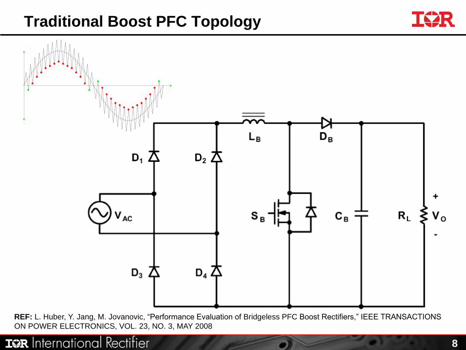
Traditional Boost PFC Topology
8
REF: L. Huber, Y. Jang, M. Jovanovic, “Performance Evaluation of Bridgeless PFC Boost Rectifiers,” IEEE TRANSACTIONS
ON POWER ELECTRONICS, VOL. 23, NO. 3, MAY 2008

Qoss Stored Energy versus Vds
9
0
5
10
15
20
25
30
35
40
0 100 200 300 400 500 600
Sto
red
En
erg
y (
µJ)
Vds (Volts)
IPW65R045C7
18.6µJ @ 400V
IPW60R045CP
25.7µJ @ 400V
50mΩ GaN Cascode
17.1µJ @ 400V
Company Confidential
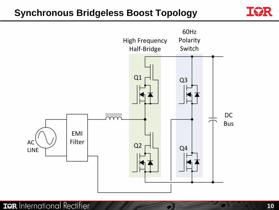
Synchronous Bridgeless Boost Topology
10
ACLINE
EMI Filter
High Frequency Half-Bridge
60Hz Polarity Switch
DC Bus
Q1
Q2
Q3
Q4

600 V Device Trr Performance Comparison
GaN Qrr independent of temperature
Pulse
Switching
FET
DUT
vS
coaxial
DC
Bus
+
–
shunt
L
iS
iDiL
11
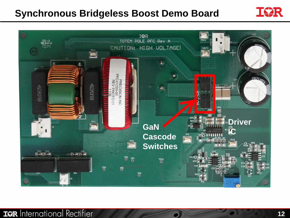
Synchronous Bridgeless Boost Demo Board
12
Driver
IC GaN
Cascode
Switches
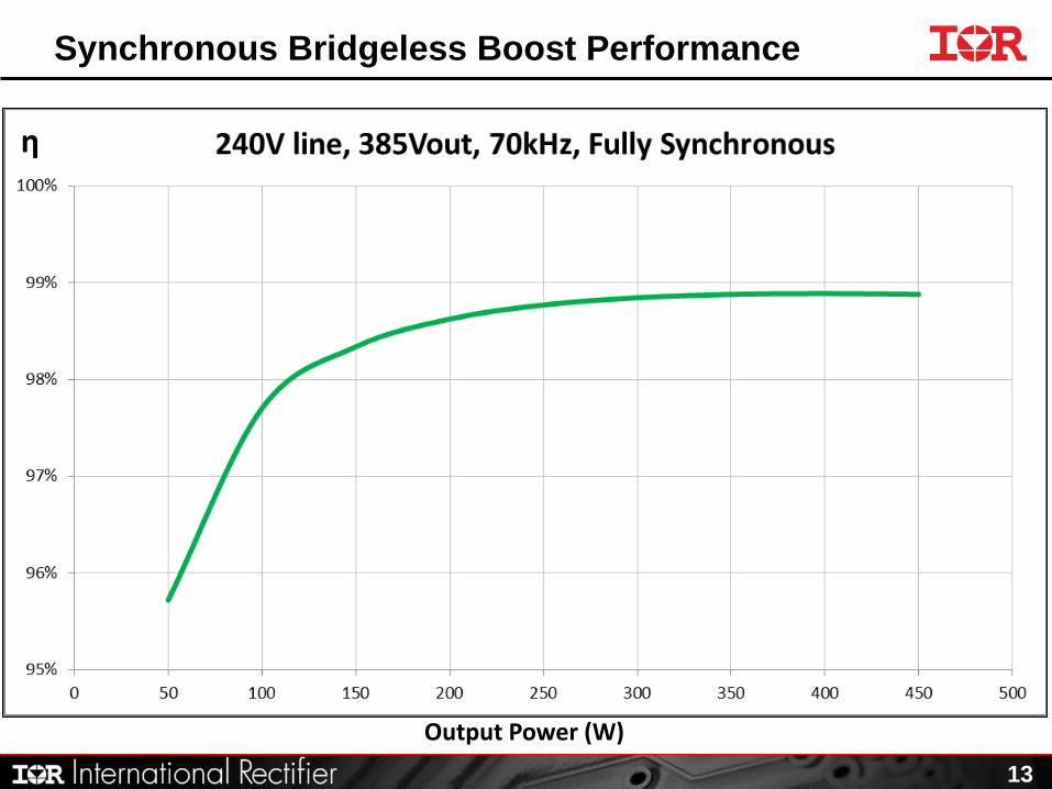
Synchronous Bridgeless Boost Performance
13
Output Power (W)
η
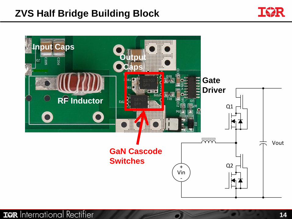
ZVS Half Bridge Building Block
14
Vout
Q1
Q2+
-Vin
Input Caps
Output
Caps
RF Inductor
Gate
Driver
GaN Cascode
Switches

Half-Bridge Voltage and Current @ 3.3 MHz
15
+6 A
+4 A
+2 A
0 A
-2 A
0 V
100 V
200 V
300 V
400 V
Inductor Current
Switch Voltage

Performance of Half-Bridge Boost
16
80%
82%
84%
86%
88%
90%
92%
94%
96%
98%
100%
0 100 200 300 400 500
Eff
icie
ncy
Po [W]
Boost Converter Efficiency, No Heatsink, 400 V Out
2.5 MHz
3.3 MHz
High Efficiency Possible by Frequency Control

High-Frequency ZVS Boost Summary
17
• 500 W, 2.5 MHz, 97% efficiency – NOT Possible with Silicon
• Very small magnetic – 18 mm toroid inductor
• No heatsink – convection cooled
• Very low gate drive power – 0.72 W consumed by gate driver
• Enables ZVS Boost PFC

LLC Resonant DC-DC Power Supply
18

Nonlinear Qoss Causes Time Delay
19
0
50
100
150
200
250
300
350
400
450
500
0 10 20 30 40 50 60 70 80 90 100 110 120 130 140 150
Vo
lts
Time (µs)
3.3X longer charge-up time
Qoss Measurement Circuit
Company Confidential

LLC – GaN vs SuperJunction @ 1 MHz
20
• GaN losses are significantly lower than SuperJunction
IPP65R150CFD2 GaN Vds
Vgs
iprim
icentertap
I2 Primary I2 Secondary Gate Drive
GaN 3.84 A2 48.0 A2 0.24 W
SuperJunction 4.93 A2 64.6 A2 1.88 W
Difference +28.3% +34.6% +685%

Conducted EMI Benefits of GaN
21
GaN IR 20 kHz IGBT 20 kHz Rg = 2 Ω
• Test condition: single half-bridge 1.5 A phase current 20 kHz
• No EMI filter
• GaN is up to 45 dB improvement over Si IGBT
45 dB Improvement at 1.5 MHz
Test data courtesy of Schneider Electronic ,Technology & Strategy Department

The Future?
22
• Integration – IPMs
• Multiphase Architectures
• Short-circuit capability
• 900 V GaN
• VHF Optimized 30 MHz+


