


Languages
Pages
Legal


10p PhD Course 18 Lectures Nov-Dec 2011 and Jan – Feb 2012 Literature Semiconductor Physics – K. Seeger The Physics of Semiconductors – Grundmann Basic Semiconductors Physics - Hamaguchi Electronic and Optoelectronic Properties of Semiconductors - Singh Quantum Well Wires and Dots – Hartmann Wave Mechanics Applied to Semiconductor Heterostructures - Bastard Fundamentals of Semiconductor Physics and Devices – Enderlein & Horing Examination Homework Problems (6p) Written Exam (4p) Additionally Your own research area. Background courses (Solid State Physics, SC Physics, Sc Devices)
Semiconductor Physics
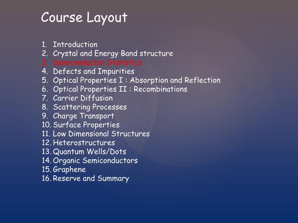
1. Introduction 2. Crystal and Energy Band structure 3. Semiconductor Statistics 4. Defects and Impurities 5. Optical Properties I : Absorption and Reflection 6. Optical Properties II : Recombinations 7. Carrier Diffusion 8. Scattering Processes 9. Charge Transport 10. Surface Properties 11. Low Dimensional Structures 12. Heterostructures 13. Quantum Wells/Dots 14. Organic Semiconductors 15. Graphene 16. Reserve and Summary
Course Layout
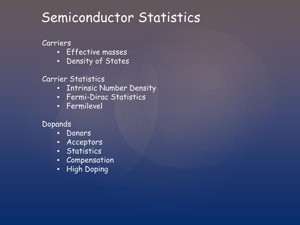
Carriers • Effective masses • Density of States
Carrier Statistics
• Intrinsic Number Density • Fermi-Dirac Statistics • Fermilevel
Dopands
• Donors • Acceptors • Statistics • Compensation • High Doping
Semiconductor Statistics

Bandstructure
Reciprocal Space Real Space Constant Energy Surdaces
For free electron
For electron in a crystal

Effective Mass Effective mass are anistropic Strongly in materials with diamond like structure, such as Si Weakly for semiconductor with wurtzite structure, such as GaAs Polaronic effect: In crystals with ionic binding a moving electron polarizes
the Ions.
Nonparabolocity: Energy momentum dispersion is only parabolic for small k-values. Deviates at higher energies.
α Fröhlich Coupling Constant
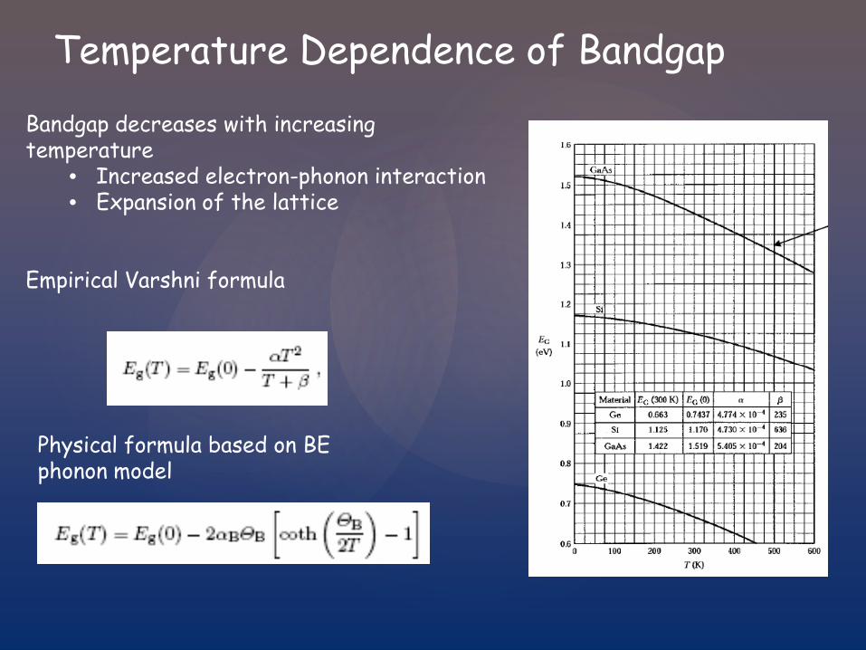
Temperature Dependence of Bandgap Bandgap decreases with increasing temperature
• Increased electron-phonon interaction • Expansion of the lattice
Empirical Varshni formula
Physical formula based on BE phonon model
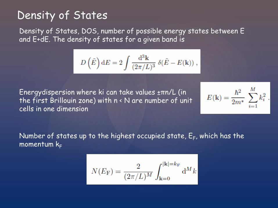
Density of States Density of States, DOS, number of possible energy states between E and E+dE. The density of states for a given band is
Energydispersion where ki can take values ±πn/L (in the first Brillouin zone) with n < N are number of unit cells in one dimension
Number of states up to the highest occupied state, EF, which has the momentum kF
Density of States
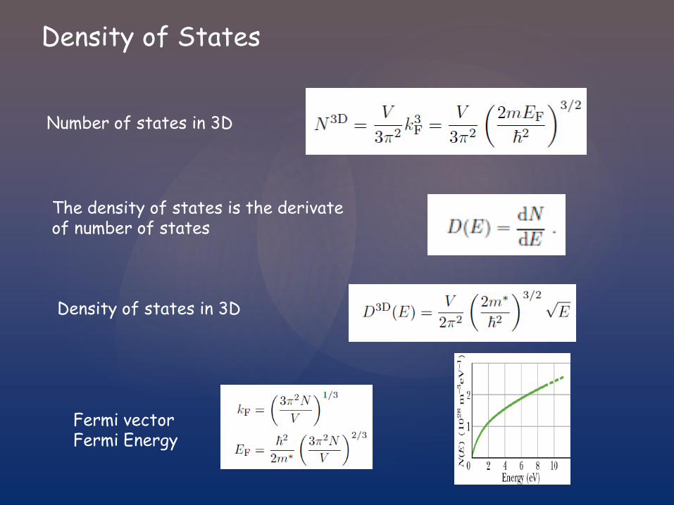
Number of states in 3D
Fermi vector Fermi Energy
Density of states in 3D
The density of states is the derivate of number of states
Fermi-Dirac Statistics
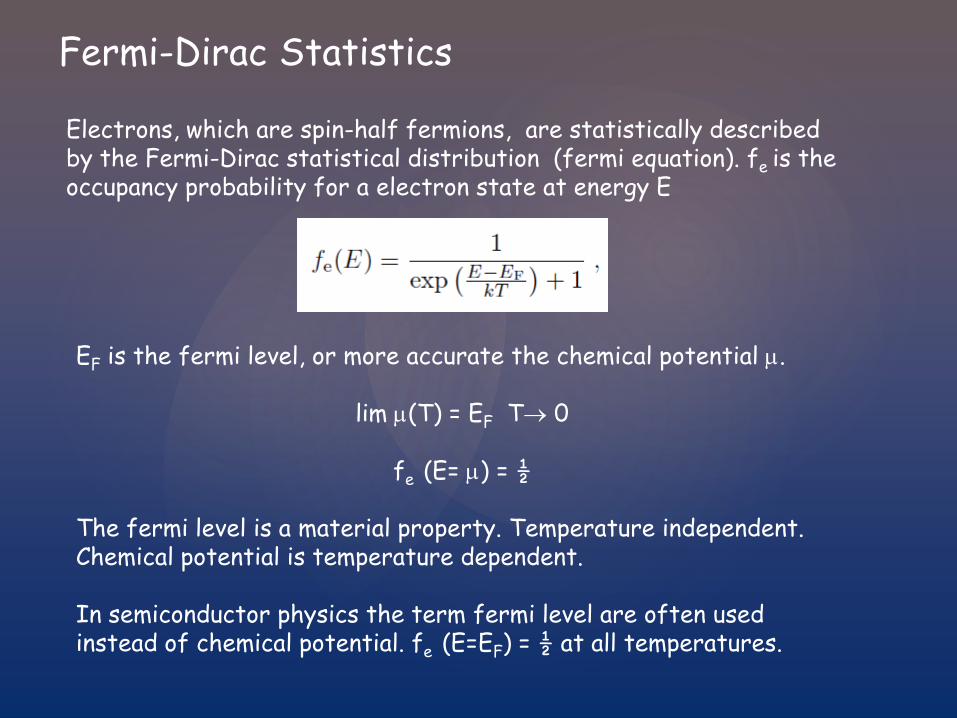
Electrons, which are spin-half fermions, are statistically described by the Fermi-Dirac statistical distribution (fermi equation). fe is the occupancy probability for a electron state at energy E
EF is the fermi level, or more accurate the chemical potential µ.
lim µ(T) = EF T→ 0
fe (E= µ) = ½
The fermi level is a material property. Temperature independent. Chemical potential is temperature dependent. In semiconductor physics the term fermi level are often used instead of chemical potential. fe (E=EF) = ½ at all temperatures.
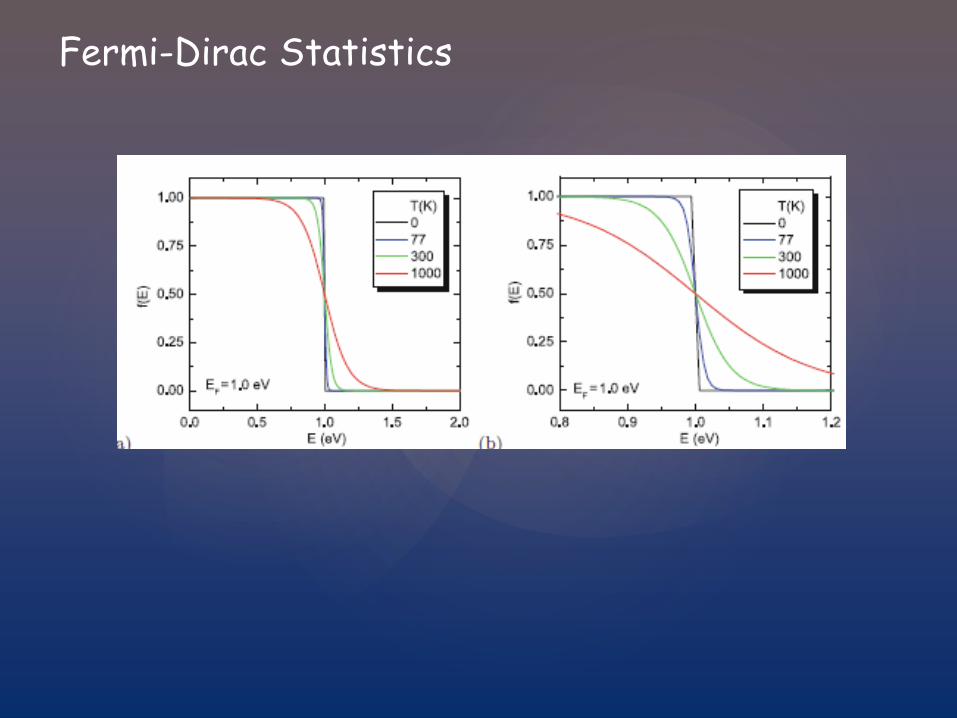
Fermi-Dirac Statistics

Boltzmann approximation
The fermi-dirac distribution are often approximated by the Boltzmann distribution.
Boltzmann approximation not possible: • At high temperatures • Low bandgaps • Close to bandedges.
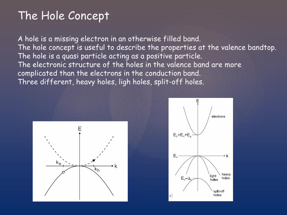
The Hole Concept
A hole is a missing electron in an otherwise filled band. The hole concept is useful to describe the properties at the valence bandtop. The hole is a quasi particle acting as a positive particle. The electronic structure of the holes in the valence band are more complicated than the electrons in the conduction band. Three different, heavy holes, ligh holes, split-off holes.
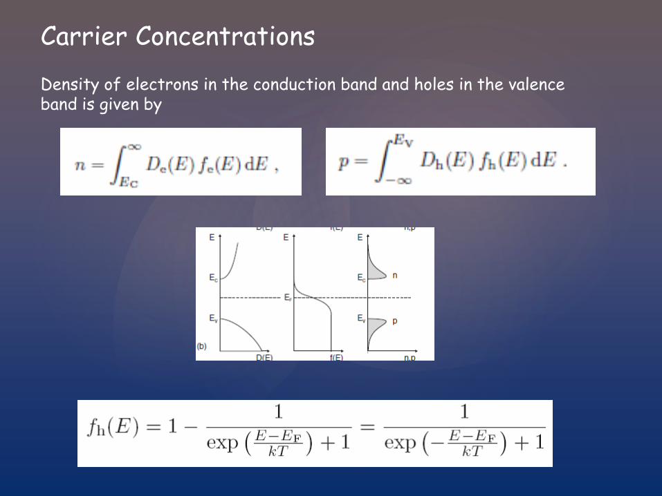
Carrier Concentrations Density of electrons in the conduction band and holes in the valence band is given by

Carrier Concentrations With the Boltzmann approximation this can be analytically solved to give electron density in the conduction band as
And hole density in the valence band as
With and an effective hole mass mh as
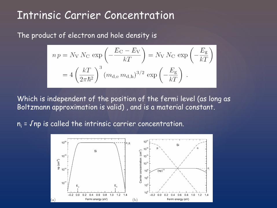
Intrinsic Carrier Concentration The product of electron and hole density is
Which is independent of the position of the fermi level (as long as Boltzmann approximation is valid) , and is a material constant. ni = √np is called the intrinsic carrier concentration.
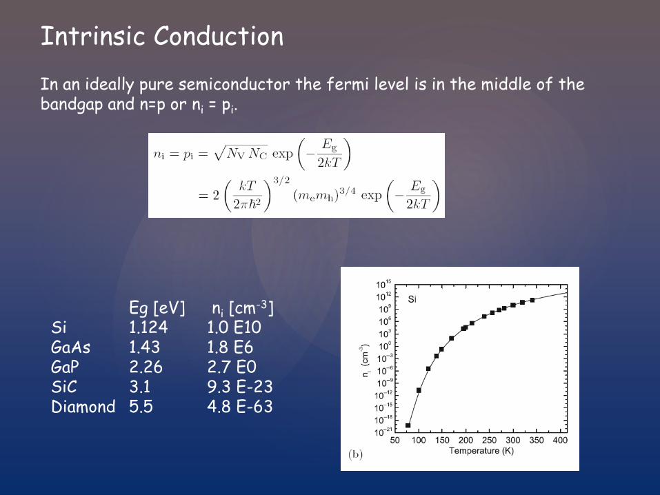
Intrinsic Conduction In an ideally pure semiconductor the fermi level is in the middle of the bandgap and n=p or ni = pi.
Eg [eV] ni [cm-3] Si 1.124 1.0 E10 GaAs 1.43 1.8 E6 GaP 2.26 2.7 E0 SiC 3.1 9.3 E-23 Diamond 5.5 4.8 E-63

Defects Point Defects Vacancy – The vacancy created by a missing atom A is denoted VA. Interstitial – An atom occupying an insterstitional site is denoted IA. Substitutional – An atom C replacing a host atom A is denoted CA. Antisite – When a host atom B occupies the site of another host atom A Intrinsic Defects – Defects involving host atoms. Extrinsic Defects – Defects including foreign impurities. Shallow defects
• Energylevels close to the valence or conduction band • The coulomb part of the ion-core determines the energy level • The defect wavefunction is given by the Bohr radius • Actings as dopands
Deep defects • Energylevel away from the bandedges • Short range part of the potential determines energylevel • Wavefunction in the order of the lattice constant • Normally non-wanted defects

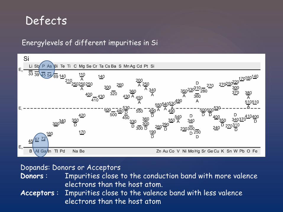
Defects
Energylevels of different impurities in Si
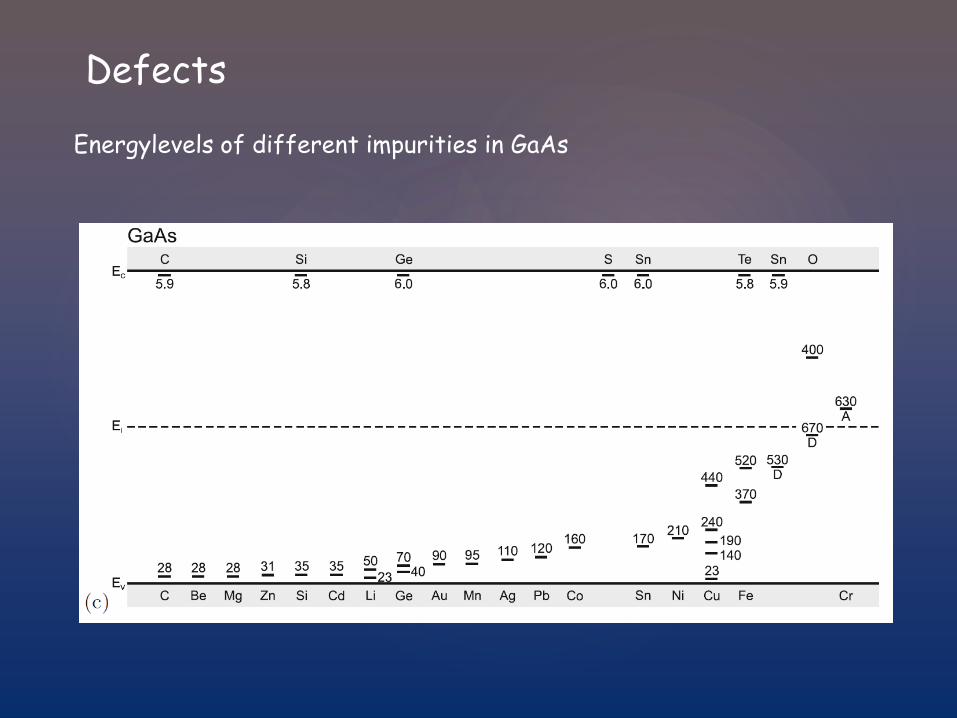
Defects
Energylevels of different impurities in GaAs
Defects
Energylevels of different impurities in Si
Dopands: Donors or Acceptors Donors : Impurities close to the conduction band with more valence
electrons than the host atom. Acceptors : Impurities close to the valence band with less valence
electrons than the host atom
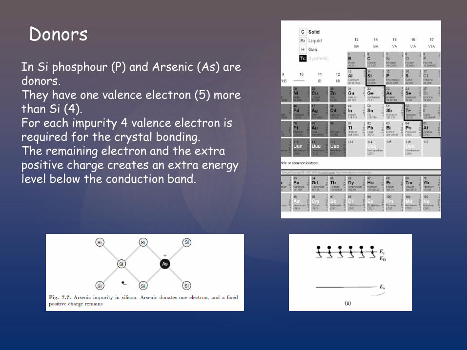
Donors In Si phosphour (P) and Arsenic (As) are donors. They have one valence electron (5) more than Si (4). For each impurity 4 valence electron is required for the crystal bonding. The remaining electron and the extra positive charge creates an extra energy level below the conduction band.
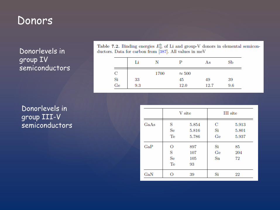
Donors
Donorlevels in group IV semiconductors
Donorlevels in group III-V semiconductors

Effective Mass Theory
In Effective-Mass Theory (EMT) the energy levels of the donor is obtained from Bohr’s theory for the hydrogen atom. The energy level for the electron in hydrogen is scaled with the ratio of the effective mass to the free electron mass and with the relative dielectric constant. For Si the EMT energy level is 6 meV, below The conduction band edge (hydrogen continuum) More detailed calculation using the Anisotropic effective mass gives 9.05 meV.
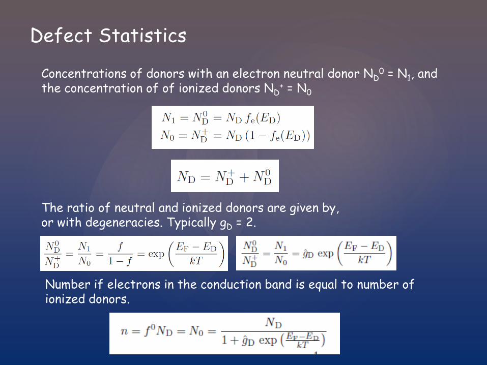
Defect Statistics
Concentrations of donors with an electron neutral donor ND0 = N1, and
the concentration of of ionized donors ND+ = N0
The ratio of neutral and ionized donors are given by, or with degeneracies. Typically gD = 2.
Number if electrons in the conduction band is equal to number of ionized donors.
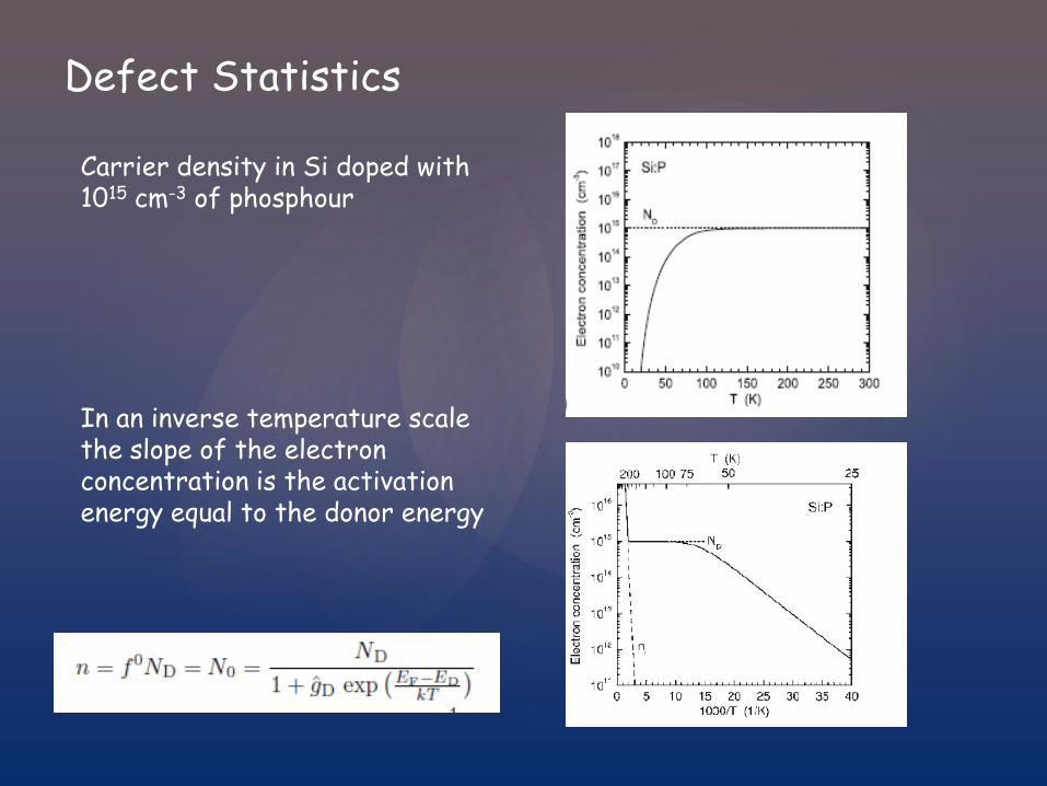
Defect Statistics
Carrier density in Si doped with 1015 cm-3 of phosphour In an inverse temperature scale the slope of the electron concentration is the activation energy equal to the donor energy
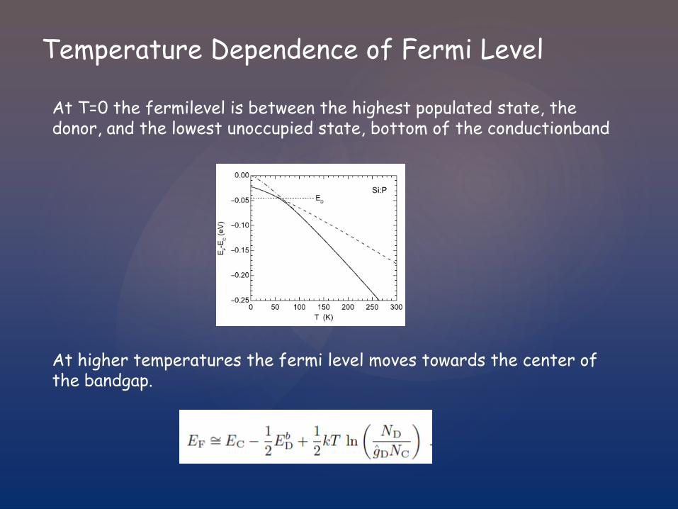
Temperature Dependence of Fermi Level
At T=0 the fermilevel is between the highest populated state, the donor, and the lowest unoccupied state, bottom of the conductionband
At higher temperatures the fermi level moves towards the center of the bandgap.

Semiconductor Conductivity
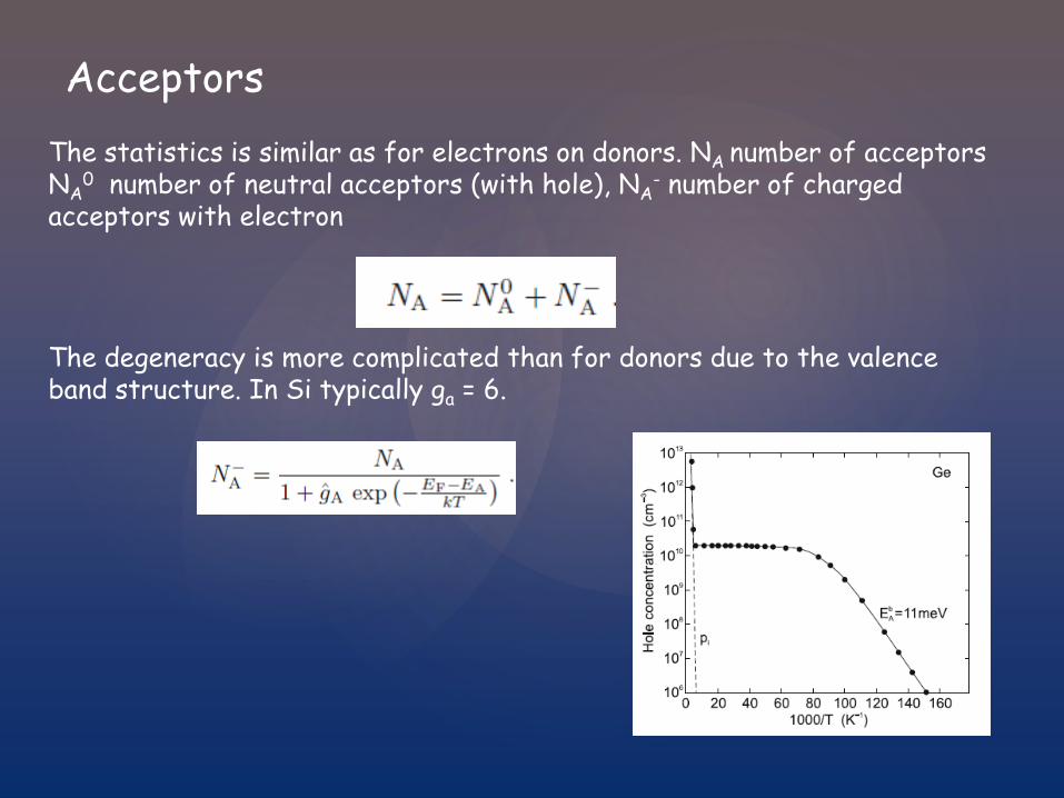
Acceptors The statistics is similar as for electrons on donors. NA number of acceptors NA
0 number of neutral acceptors (with hole), NA- number of charged
acceptors with electron
The degeneracy is more complicated than for donors due to the valence band structure. In Si typically ga = 6.

Acceptors An acceptor has less valence electrons than the host. In Si Bor (B) and Aluminum (Al) are acceptors. They have one valence electron (3) less than Si (4). One electron is missing to make the bonds, which is captured from the valence band, leaving a hole. Alternatively, the hole on the acceptor is excited into the valence band.

Acceptors Some acceptors have levels close to the effective mass value while some are much higher. Semiconductors where the conductivity is by holes are labelled p-type materials.

Temperature Dependence of Fermi Level
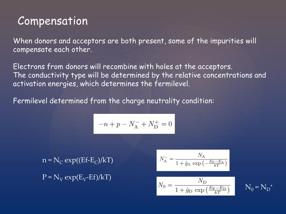
Compensation When donors and acceptors are both present, some of the impurities will compensate each other. Electrons from donors will recombine with holes at the acceptors. The conductivity type will be determined by the relative concentrations and activation energies, which determines the fermilevel. Fermilevel determined from the charge neutrality condition:
N0 = ND+
n = NC exp((Ef-EC)/kT) P = NV exp(EV-Ef)/kT)

Compensation We assume Boltzmann statistics ND > NA material will be n-type p = 0 and NA
- = NA The charge neutrality simplifies to: After some algebra:
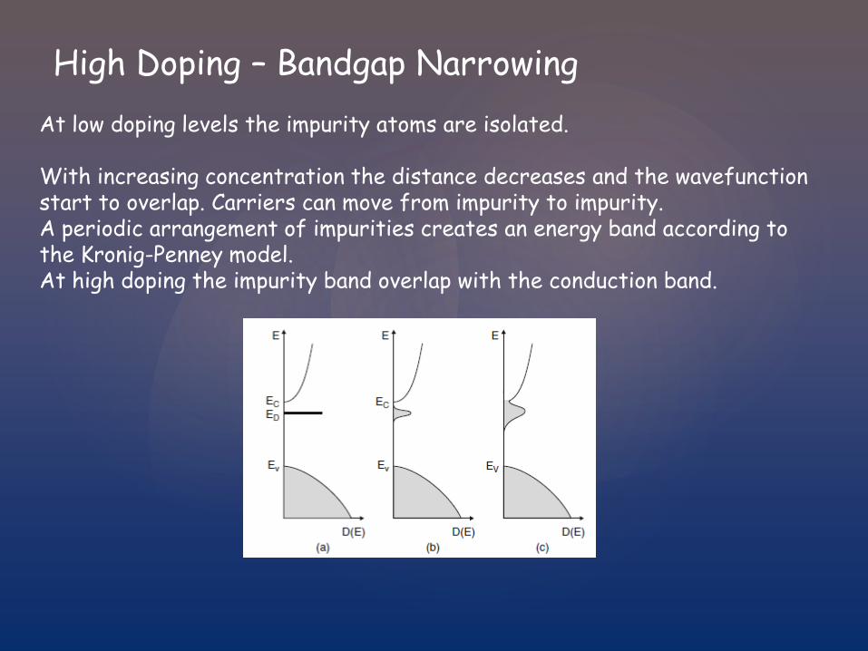
High Doping – Bandgap Narrowing At low doping levels the impurity atoms are isolated. With increasing concentration the distance decreases and the wavefunction start to overlap. Carriers can move from impurity to impurity. A periodic arrangement of impurities creates an energy band according to the Kronig-Penney model. At high doping the impurity band overlap with the conduction band.
High Doping – Bandgap Narrowing
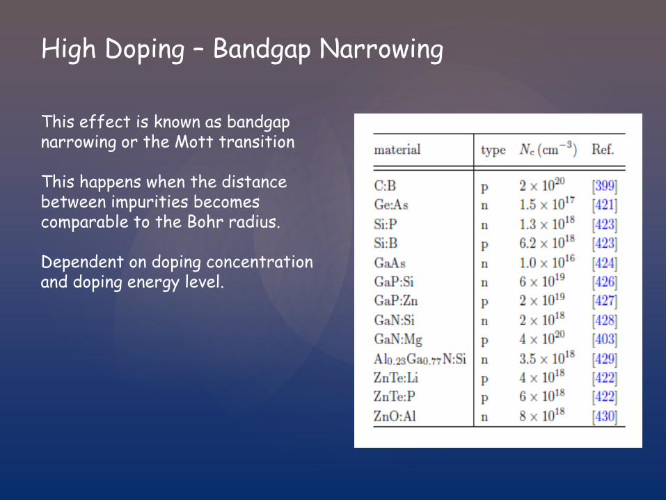
This effect is known as bandgap narrowing or the Mott transition This happens when the distance between impurities becomes comparable to the Bohr radius. Dependent on doping concentration and doping energy level.

Quasi Fermi Levels
The statistics has sofar only considered semiconductors in thermal equilibrium. During non-equilibrium conditions, e.g. external excitation or carrier injection, the electron and hole densities can take arbitrarily forms. The fermi level is not constant through the structure. There will instead be separate quasi-fermi levels for electrons and holes, respectively. F½ is the Fermi function, and Fn(r) and Fp(r) the quasi fermi levels.
Top Related