![Process Optimization for Flexible Printed Circuit Board ...129-135).pdf · Process Optimization for Flexible Printed Circuit Board ... ing was applied to the electronic products [4].](https://static.fdocuments.in/doc/165x107/5a87aba37f8b9a9f1b8dec9f/process-optimization-for-flexible-printed-circuit-board-129-135pdfprocess.jpg)


Languages
Pages
Legal

National Aeronautics and Space Administration
www.nasa.govS a f e l y A c h i e v e A m a z i n g S c i e n c e
T h r o u g h M i s s i o n S u c c e s s
S A F E T Y a n d M I S S I O N A S S U R A N C E
D I R E C T O R A T E C o d e 3 0 0
Printed Circuit Board Quality
Assurance
Bhanu Sood
Reliability and Risk Assessment Branch
Quality and Reliability Division
https://ntrs.nasa.gov/search.jsp?R=20170005671 2020-04-06T15:01:05+00:00Z
S A F E T Y a n d M I S S I O N A S S U R A N C E D I R E C T O R AT E C o d e 3 0 0 2
Outline
•Introduction to PCBs
•PCB requirements and quality verification
•Risk assessment
•Example
S A F E T Y a n d M I S S I O N A S S U R A N C E D I R E C T O R AT E C o d e 3 0 0
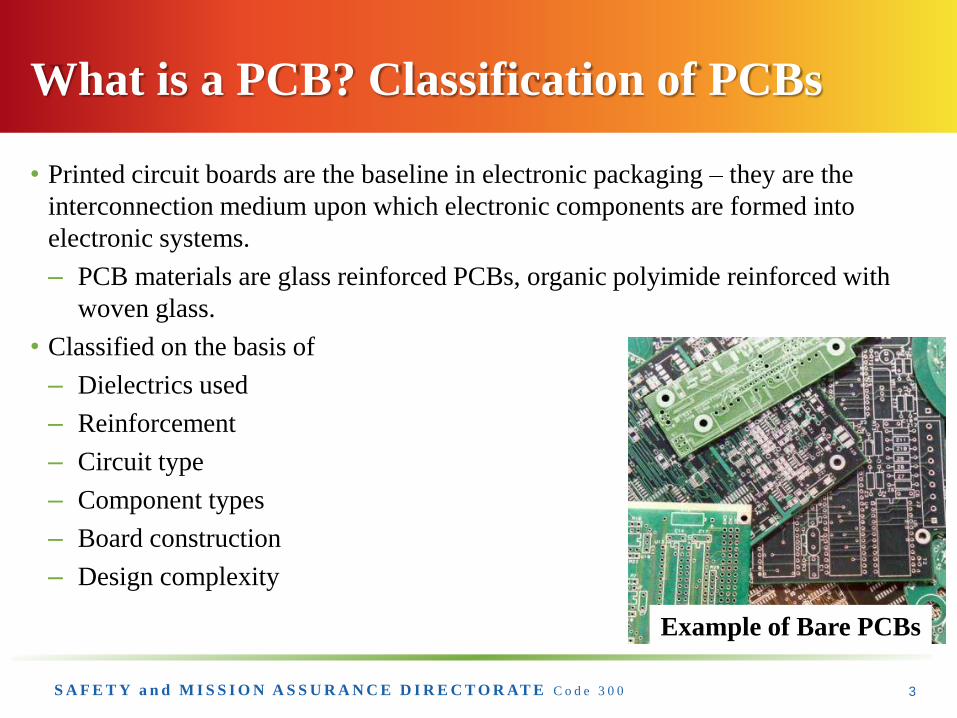
• Printed circuit boards are the baseline in electronic packaging – they are the
interconnection medium upon which electronic components are formed into
electronic systems.
– PCB materials are glass reinforced PCBs, organic polyimide reinforced with
woven glass.
• Classified on the basis of
– Dielectrics used
– Reinforcement
– Circuit type
– Component types
– Board construction
– Design complexity
What is a PCB? Classification of PCBs
Example of Bare PCBs
3
S A F E T Y a n d M I S S I O N A S S U R A N C E D I R E C T O R AT E C o d e 3 0 0
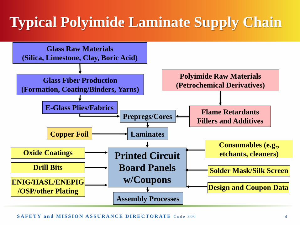
Typical Polyimide Laminate Supply Chain
Drill Bits
Glass Raw Materials
(Silica, Limestone, Clay, Boric Acid)
Design and Coupon Data
Glass Fiber Production
(Formation, Coating/Binders, Yarns)
E-Glass Plies/Fabrics
Polyimide Raw Materials
(Petrochemical Derivatives)
Prepregs/Cores
Laminates
Solder Mask/Silk Screen
ENIG/HASL/ENEPIG
/OSP/other Plating
Printed Circuit
Board Panels
w/Coupons
Copper Foil
Oxide CoatingsConsumables (e.g.,
etchants, cleaners)
Flame Retardants
Fillers and Additives
Assembly Processes
4
S A F E T Y a n d M I S S I O N A S S U R A N C E D I R E C T O R AT E C o d e 3 0 0
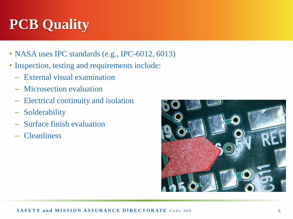
• NASA uses IPC standards (e.g., IPC-6012, 6013)
• Inspection, testing and requirements include:
– External visual examination
– Microsection evaluation
– Electrical continuity and isolation
– Solderability
– Surface finish evaluation
– Cleanliness
PCB Quality
5
S A F E T Y a n d M I S S I O N A S S U R A N C E D I R E C T O R AT E C o d e 3 0 0
Significance of Board Requirements
6
• The requirements and coupons are a “front door”.
• Examples:
– Internal Annular Ring:
• Egregious violations indicate there may have been a serious
problem in development of the board.
• Minor violations don’t likely indicate any risk at all (IPC-6012DS)
– Negative etchback:
• With modern cleaning processes and flight experience can result in
higher reliability with negative etchback.
– Wicking of copper:
• Requirements are conservative based on broad statistics.
• A basic analysis of the board layout can indicate directly if there is
risk or not, regardless of requirements violations.
S A F E T Y a n d M I S S I O N A S S U R A N C E D I R E C T O R AT E C o d e 3 0 0
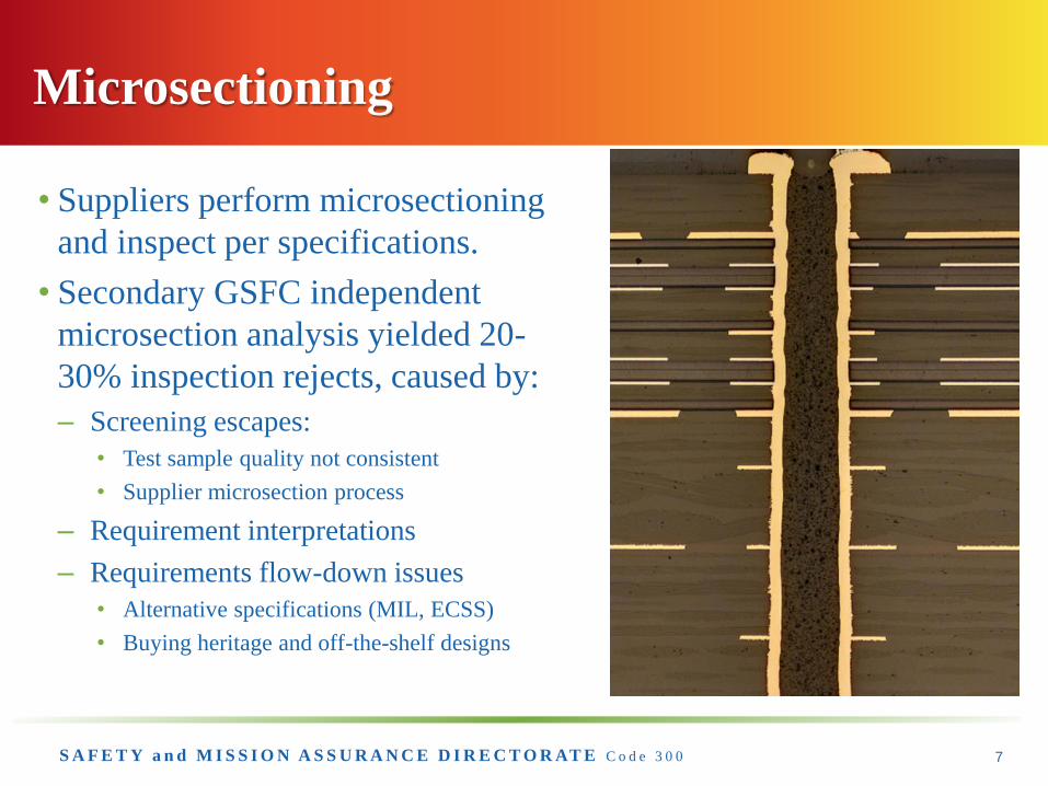
Microsectioning
7
• Suppliers perform microsectioning
and inspect per specifications.
• Secondary GSFC independent
microsection analysis yielded 20-
30% inspection rejects, caused by:
– Screening escapes:
• Test sample quality not consistent
• Supplier microsection process
– Requirement interpretations
– Requirements flow-down issues
• Alternative specifications (MIL, ECSS)
• Buying heritage and off-the-shelf designs
S A F E T Y a n d M I S S I O N A S S U R A N C E D I R E C T O R AT E C o d e 3 0 0
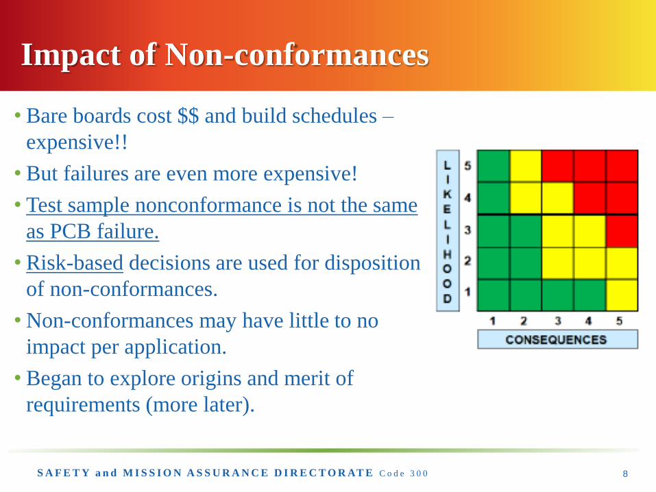
Impact of Non-conformances
8
• Bare boards cost $$ and build schedules –
expensive!!
• But failures are even more expensive!
• Test sample nonconformance is not the same
as PCB failure.
• Risk-based decisions are used for disposition
of non-conformances.
• Non-conformances may have little to no
impact per application.
• Began to explore origins and merit of
requirements (more later).
S A F E T Y a n d M I S S I O N A S S U R A N C E D I R E C T O R AT E C o d e 3 0 0
• Traceable PCB test coupons (designed per specs. such as IPC-2221B)
are submitted to GSFC or to a GSFC-assessed laboratory.
• Reports that indicate nonconformance are dispositioned by risk
assessment performed prior to refabricating or populating the PCB.
– If risk assessment indicates elevated risk due to the
nonconformance, then use is dispositioned by MRB.
• More than a 100 PCB lots assessed for risk since 2014, 95%
dispositioned as UAI, significant cost and schedule savings.
• Risk assessment process eliminates waste and saves money and
schedule, lowers overall risk for the project.
• The process reduces the need for repeated attempts to refabricate.
Risk Assessment
9

S A F E T Y a n d M I S S I O N A S S U R A N C E D I R E C T O R AT E C o d e 3 0 0
Example: PTH Copper Wrap Thickness
Requirement
10
Per IPC-6012D for through-holes:
AABUS = As Agreed Between User and Supplier
Class 1 AABUS
Class 2 5 µm [197 µin]
Class 3 & 3/A 12 µm [472 µin]
•Thermal cycle stresses
act on interfaces, outer
layers experience the
greatest stress.
•Reason: materials
selection and geometry.
S A F E T Y a n d M I S S I O N A S S U R A N C E D I R E C T O R AT E C o d e 3 0 0 11
PTH Copper Wrap Thickness: Disposition
• Mission had populated and integrated board with zero wrap, wrap planarization can cause
0.3mil or more variance in panel; manufacturers must target more wrap.
– Wrap cannot be achieved at required thickness for designs with tight line-width spacing
and/or with multiple lamination/plating steps
• Requirement was introduced to IPC with minimal data
– Reliability reported to be better with wrap vs. butt joint
– Half of barrel plating thought to be “good enough”
– Higher quality limit used as safety margin against manufacturing variation during
planarization
• GSFC Studies: Determined the impact of copper wrap plating thickness on PCB reliability,
as characterized by thermal cycles to failure.
– Able to determine acceptability of wrap defect based on reliability testing and analysis in
context of mission environment and duration.
– IPC voted to change the requirement (amendment in Rev. D and revisions in Rev. E).
S A F E T Y a n d M I S S I O N A S S U R A N C E D I R E C T O R AT E C o d e 3 0 0
• PCB assurance actives are informed by risk in context of the
Project.
• Lessons are being applied across Projects for continuous
improvements.
• Newer component technologies, smaller/high pitch devices:
tighter and more demanding PCB designs:
– Identifying new research areas.
– New materials, designs, structures and test methods.
PCB Assurance: Summary
12
S A F E T Y a n d M I S S I O N A S S U R A N C E D I R E C T O R AT E C o d e 3 0 0
Bhanu Sood
Commodity Risk Assessment Engineer
Code 371 – Reliability and Risk Assessment Branch
NASA Goddard Space Flight Center
Phone: (301) 286-5584
Thank you!
13

S A F E T Y a n d M I S S I O N A S S U R A N C E D I R E C T O R AT E C o d e 3 0 0 14
Top Related