Printed Circuit Board Quality Assurance - NASA · •Printed circuit boards are the baseline in...
14
National Aeronautics and Space Administration www.nasa.gov Safely Achieve Amazing Science Through Mission Success SAFETY and MISSION ASSURANCE DIRECTORATE Code 300 Printed Circuit Board Quality Assurance Bhanu Sood Reliability and Risk Assessment Branch Quality and Reliability Division https://ntrs.nasa.gov/search.jsp?R=20170005671 2020-04-06T15:01:05+00:00Z
Transcript of Printed Circuit Board Quality Assurance - NASA · •Printed circuit boards are the baseline in...
National Aeronautics and Space Administration
www.nasa.govS a f e l y A c h i e v e A m a z i n g S c i e n c e
T h r o u g h M i s s i o n S u c c e s s
S A F E T Y a n d M I S S I O N A S S U R A N C E
D I R E C T O R A T E C o d e 3 0 0
Printed Circuit Board Quality
Assurance
Bhanu Sood
Reliability and Risk Assessment Branch
Quality and Reliability Division
https://ntrs.nasa.gov/search.jsp?R=20170005671 2020-04-06T15:01:05+00:00Z
S A F E T Y a n d M I S S I O N A S S U R A N C E D I R E C T O R AT E C o d e 3 0 0 2
Outline
•Introduction to PCBs
•PCB requirements and quality verification
•Risk assessment
•Example
S A F E T Y a n d M I S S I O N A S S U R A N C E D I R E C T O R AT E C o d e 3 0 0
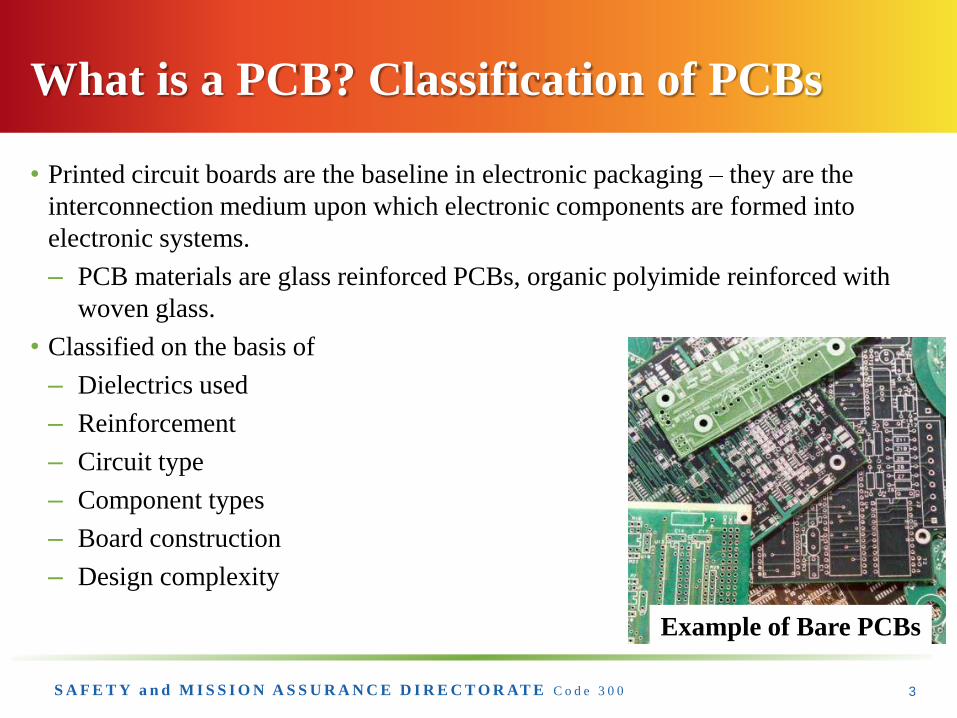
• Printed circuit boards are the baseline in electronic packaging – they are the
interconnection medium upon which electronic components are formed into
electronic systems.
– PCB materials are glass reinforced PCBs, organic polyimide reinforced with
woven glass.
• Classified on the basis of
– Dielectrics used
– Reinforcement
– Circuit type
– Component types
– Board construction
– Design complexity
What is a PCB? Classification of PCBs
Example of Bare PCBs
3
S A F E T Y a n d M I S S I O N A S S U R A N C E D I R E C T O R AT E C o d e 3 0 0
Typical Polyimide Laminate Supply Chain
Drill Bits
Glass Raw Materials
(Silica, Limestone, Clay, Boric Acid)
Design and Coupon Data
Glass Fiber Production
(Formation, Coating/Binders, Yarns)
E-Glass Plies/Fabrics
Polyimide Raw Materials
(Petrochemical Derivatives)
Prepregs/Cores
Laminates
Solder Mask/Silk Screen
ENIG/HASL/ENEPIG
/OSP/other Plating
Printed Circuit
Board Panels
w/Coupons
Copper Foil
Oxide CoatingsConsumables (e.g.,
etchants, cleaners)
Flame Retardants
Fillers and Additives
Assembly Processes
4
S A F E T Y a n d M I S S I O N A S S U R A N C E D I R E C T O R AT E C o d e 3 0 0
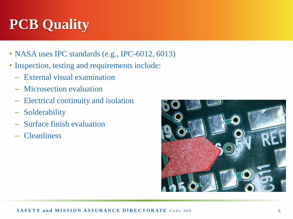
• NASA uses IPC standards (e.g., IPC-6012, 6013)
• Inspection, testing and requirements include:
– External visual examination
– Microsection evaluation
– Electrical continuity and isolation
– Solderability
– Surface finish evaluation
– Cleanliness
PCB Quality
5
S A F E T Y a n d M I S S I O N A S S U R A N C E D I R E C T O R AT E C o d e 3 0 0
Significance of Board Requirements
6
• The requirements and coupons are a “front door”.
• Examples:
– Internal Annular Ring:
• Egregious violations indicate there may have been a serious
problem in development of the board.
• Minor violations don’t likely indicate any risk at all (IPC-6012DS)
– Negative etchback:
• With modern cleaning processes and flight experience can result in
higher reliability with negative etchback.
– Wicking of copper:
• Requirements are conservative based on broad statistics.
• A basic analysis of the board layout can indicate directly if there is
risk or not, regardless of requirements violations.
S A F E T Y a n d M I S S I O N A S S U R A N C E D I R E C T O R AT E C o d e 3 0 0
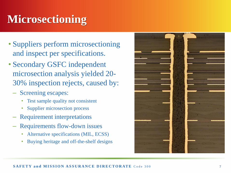
Microsectioning
7
• Suppliers perform microsectioning
and inspect per specifications.
• Secondary GSFC independent
microsection analysis yielded 20-
30% inspection rejects, caused by:
– Screening escapes:
• Test sample quality not consistent
• Supplier microsection process
– Requirement interpretations
– Requirements flow-down issues
• Alternative specifications (MIL, ECSS)
• Buying heritage and off-the-shelf designs
S A F E T Y a n d M I S S I O N A S S U R A N C E D I R E C T O R AT E C o d e 3 0 0
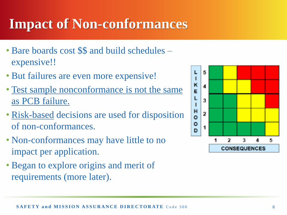
Impact of Non-conformances
8
• Bare boards cost $$ and build schedules –
expensive!!
• But failures are even more expensive!
• Test sample nonconformance is not the same
as PCB failure.
• Risk-based decisions are used for disposition
of non-conformances.
• Non-conformances may have little to no
impact per application.
• Began to explore origins and merit of
requirements (more later).
S A F E T Y a n d M I S S I O N A S S U R A N C E D I R E C T O R AT E C o d e 3 0 0
• Traceable PCB test coupons (designed per specs. such as IPC-2221B)
are submitted to GSFC or to a GSFC-assessed laboratory.
• Reports that indicate nonconformance are dispositioned by risk
assessment performed prior to refabricating or populating the PCB.
– If risk assessment indicates elevated risk due to the
nonconformance, then use is dispositioned by MRB.
• More than a 100 PCB lots assessed for risk since 2014, 95%
dispositioned as UAI, significant cost and schedule savings.
• Risk assessment process eliminates waste and saves money and
schedule, lowers overall risk for the project.
• The process reduces the need for repeated attempts to refabricate.
Risk Assessment
9

S A F E T Y a n d M I S S I O N A S S U R A N C E D I R E C T O R AT E C o d e 3 0 0
Example: PTH Copper Wrap Thickness
Requirement
10
Per IPC-6012D for through-holes:
AABUS = As Agreed Between User and Supplier
Class 1 AABUS
Class 2 5 µm [197 µin]
Class 3 & 3/A 12 µm [472 µin]
•Thermal cycle stresses
act on interfaces, outer
layers experience the
greatest stress.
•Reason: materials
selection and geometry.
S A F E T Y a n d M I S S I O N A S S U R A N C E D I R E C T O R AT E C o d e 3 0 0 11
PTH Copper Wrap Thickness: Disposition
• Mission had populated and integrated board with zero wrap, wrap planarization can cause
0.3mil or more variance in panel; manufacturers must target more wrap.
– Wrap cannot be achieved at required thickness for designs with tight line-width spacing
and/or with multiple lamination/plating steps
• Requirement was introduced to IPC with minimal data
– Reliability reported to be better with wrap vs. butt joint
– Half of barrel plating thought to be “good enough”
– Higher quality limit used as safety margin against manufacturing variation during
planarization
• GSFC Studies: Determined the impact of copper wrap plating thickness on PCB reliability,
as characterized by thermal cycles to failure.
– Able to determine acceptability of wrap defect based on reliability testing and analysis in
context of mission environment and duration.
– IPC voted to change the requirement (amendment in Rev. D and revisions in Rev. E).
S A F E T Y a n d M I S S I O N A S S U R A N C E D I R E C T O R AT E C o d e 3 0 0
• PCB assurance actives are informed by risk in context of the
Project.
• Lessons are being applied across Projects for continuous
improvements.
• Newer component technologies, smaller/high pitch devices:
tighter and more demanding PCB designs:
– Identifying new research areas.
– New materials, designs, structures and test methods.
PCB Assurance: Summary
12
S A F E T Y a n d M I S S I O N A S S U R A N C E D I R E C T O R AT E C o d e 3 0 0
Bhanu Sood
Commodity Risk Assessment Engineer
Code 371 – Reliability and Risk Assessment Branch
NASA Goddard Space Flight Center
Phone: (301) 286-5584
Thank you!
13

S A F E T Y a n d M I S S I O N A S S U R A N C E D I R E C T O R AT E C o d e 3 0 0 14


![Process Optimization for Flexible Printed Circuit Board ...129-135).pdf · Process Optimization for Flexible Printed Circuit Board ... ing was applied to the electronic products [4].](https://static.fdocuments.in/doc/165x107/5a87aba37f8b9a9f1b8dec9f/process-optimization-for-flexible-printed-circuit-board-129-135pdfprocess.jpg)