


Languages
Pages
Legal


Modern VLSI Design 2e: Chapter 3 Copyright 1998 Prentice Hall PTR
Topics
Electrical properties of static combinational gates:– transfer characteristics;– delay;– power.
Effects of parasitics on gate. Driving large loads.

Modern VLSI Design 2e: Chapter 3 Copyright 1998 Prentice Hall PTR
Logic levels
Solid logic 0/1 defined by VSS/VDD.
Inner bounds of logic values VL/VH are not directly determined by circuit properties, as in some other logic families.
logic 1
logic 0
unknown
VDD
VSS
VH
VL

Modern VLSI Design 2e: Chapter 3 Copyright 1998 Prentice Hall PTR
Logic level matching
Levels at output of one gate must be sufficient to drive next gate.

Modern VLSI Design 2e: Chapter 3 Copyright 1998 Prentice Hall PTR
Transfer characteristics
Transfer curve shows static input/output relationship - hold input voltage, measure output voltage.

Modern VLSI Design 2e: Chapter 3 Copyright 1998 Prentice Hall PTR
Inverter transfer curve

Modern VLSI Design 2e: Chapter 3 Copyright 1998 Prentice Hall PTR
Logic thresholds
Choose threshold voltages at points where slope of transfer curve = -1.
Inverter has a high gain between VIL and VIH points, low gain at outer regions of transfer curve.
Note that logic 0 and 1 regions are not equal sized, in this case, high pullup resistance leads to smaller logic 0 range.

Modern VLSI Design 2e: Chapter 3 Copyright 1998 Prentice Hall PTR
Logic threshold example

Modern VLSI Design 2e: Chapter 3 Copyright 1998 Prentice Hall PTR
Noise margin
Noise margin = voltage difference between output of one gate and input of next. Noise must exceed noise margin to make second gate produce wrong output.
In static gates, t= voltages are VDD and VSS, so noise margins are VDD-VIH and VIL-VSS.

Modern VLSI Design 2e: Chapter 3 Copyright 1998 Prentice Hall PTR
Delay
Assume ideal input (step), RC load.

Modern VLSI Design 2e: Chapter 3 Copyright 1998 Prentice Hall PTR
Delay assumptions
Assume that only one transistor is on at a time. This gives two cases:– rise time, pullup on;– fall time, pullup off.
Assume resistor model for transistor. Ignores saturation region and mischaracterizes linear region, but results are acceptable.

Modern VLSI Design 2e: Chapter 3 Copyright 1998 Prentice Hall PTR
Current through transistor
Transistor starts in saturation region, then moves to linear region.

Modern VLSI Design 2e: Chapter 3 Copyright 1998 Prentice Hall PTR
Resistive model for transistor
Average V/I at two voltages:– maximum output voltage– middle of linear region
Voltage is Vds, current is given Id at that drain voltage. Step input means that Vgs = VDD always.

Modern VLSI Design 2e: Chapter 3 Copyright 1998 Prentice Hall PTR
Resistive approximation

Modern VLSI Design 2e: Chapter 3 Copyright 1998 Prentice Hall PTR
Effective resistance
0.5m process, minimum-sized type Vdd-Vss = 5V Vdd - Vss = 3.3V
Rn 3.9k 6.8kRp 14k 25k
effective resistance of P-type is about 3.5 times effective resistance of N-type
effective resistance increases as the power supply voltage goes down

Modern VLSI Design 2e: Chapter 3 Copyright 1998 Prentice Hall PTR
Inverter delay circuit
Load is resistor + capacitor, driver is resistor.

Modern VLSI Design 2e: Chapter 3 Copyright 1998 Prentice Hall PTR
Inverter delay
Vout(t) = VDD exp{-t/(Rn+RL)/ CL}
tf = 2.2 R CL
For pullup time, use pullup resistance.
Modern VLSI Design 2e: Chapter 3 Copyright 1998 Prentice Hall PTR
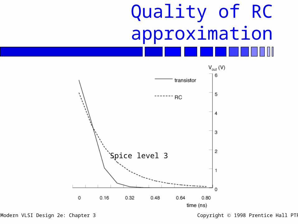
Quality of RC approximation
Spice level 3

Modern VLSI Design 2e: Chapter 3 Copyright 1998 Prentice Hall PTR
Quality of step input approximation

Modern VLSI Design 2e: Chapter 3 Copyright 1998 Prentice Hall PTR
Results of using small pullup

Modern VLSI Design 2e: Chapter 3 Copyright 1998 Prentice Hall PTR
Transistor sizing
Effective resistance depends on transistor W/L - less delay means wider transistors.
For equal pullup and pulldown times, W/L of pullup and pulldown obey Kp/Kn.

Modern VLSI Design 2e: Chapter 3 Copyright 1998 Prentice Hall PTR
Complex gates
Effective resistance of gate depends on complete pullup or pulldown network.
When evaluating NAND gate delay:– pullups are in parallel– pulldowns are in series

Modern VLSI Design 2e: Chapter 3 Copyright 1998 Prentice Hall PTR
Body effect & signal ordering
Early - arriving signal

Modern VLSI Design 2e: Chapter 3 Copyright 1998 Prentice Hall PTR
Power consumption circuit
Input is square wave.

Modern VLSI Design 2e: Chapter 3 Copyright 1998 Prentice Hall PTR
Power consumption analysis
Almost all power consumption comes from switching behavior.
Static power dissipation comes from leakage currents.
Surprising result: power consumption is independent of the sizes of the pullups and pulldowns.

Modern VLSI Design 2e: Chapter 3 Copyright 1998 Prentice Hall PTR
Leakage currents
Flow from source or drain to the substrate due to diode formed by junction.
General form of leakage current is given by diode law:– Il = Il0(eVd/kt - 1)

Modern VLSI Design 2e: Chapter 3 Copyright 1998 Prentice Hall PTR
Power consumption
A single cycle requires one charge and one discharge of capacitor: E = CL(VDD - VSS)2 .
Clock frequency f = 1/t. Power = E f = f CL(VDD - VSS)2.
Resistance of pullup/pulldown drops out of energy calculation.

Modern VLSI Design 2e: Chapter 3 Copyright 1998 Prentice Hall PTR
Parasitics and performance
b
a
c

Modern VLSI Design 2e: Chapter 3 Copyright 1998 Prentice Hall PTR
Effect of parasitics
a: Capacitance on power supply is not bad, can be good in absence of inductance. Resistance slows down static gates, may cause pseudo-nMOS circuits to fail.

Modern VLSI Design 2e: Chapter 3 Copyright 1998 Prentice Hall PTR
Effects of parasitics, cont
b: Increasing capacitance/resistance reduces input slope.
c: Similar to parasitics at b, but resistance near source is more damaging, since it must charge more capacitance.

Modern VLSI Design 2e: Chapter 3 Copyright 1998 Prentice Hall PTR
Driving large loads
Sometimes, large loads must be driven:– off-chip;– long wires on-chip.
Sizing up the driver transistors only pushes back the problem - driver now presents larger capacitance to earlier stage.

Modern VLSI Design 2e: Chapter 3 Copyright 1998 Prentice Hall PTR
Cascaded driver circuit

Modern VLSI Design 2e: Chapter 3 Copyright 1998 Prentice Hall PTR
Optimal sizing
Use a chain of inverters, each stage has transistors a larger than previous stage.
Optimal number of stages nopt = ln(Cbig/Cg).
Driver sizes are exponentially tapered.
Top Related