


Languages
Pages
Legal

ECEN 4517 1
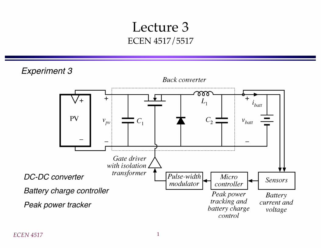
Lecture 3ECEN 4517/5517
DC-DC converterBattery charge controller
Peak power tracker
Experiment 3

ECEN 4517 2
Due dates
Tomorrow by noon, in D2L dropbox:Exp. 3 prelab assignment (one from every student)
This Friday at 5 pm:Exp. 2 scoresheet, completed (one per group)
Next week in lecture:10 minute quiz on Exp. 2. See Exp. 2 web page for a sample
ECEN 4517 3
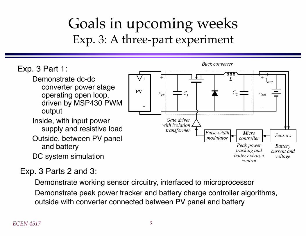
Goals in upcoming weeksExp. 3: A three-part experiment
Exp. 3 Part 1:Demonstrate dc-dc
converter power stage operating open loop, driven by MSP430 PWM output
Inside, with input power supply and resistive load
Outside, between PV panel and battery
DC system simulation
Exp. 3 Parts 2 and 3:Demonstrate working sensor circuitry, interfaced to microprocessorDemonstrate peak power tracker and battery charge controller algorithms, outside with converter connected between PV panel and battery
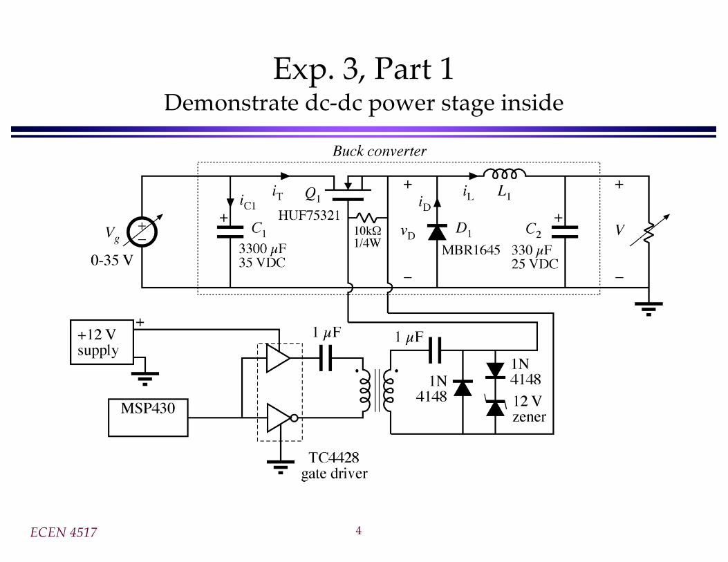
ECEN 4517 4
Exp. 3, Part 1Demonstrate dc-dc power stage inside
ECEN 4517 5
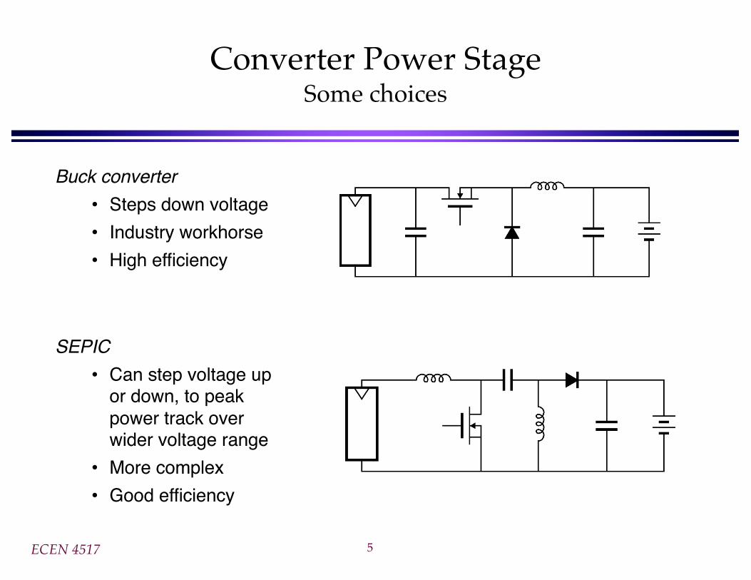
Converter Power StageSome choices
Buck converter• Steps down voltage• Industry workhorse• High efficiency
SEPIC• Can step voltage up
or down, to peak power track over wider voltage range
• More complex• Good efficiency

ECEN 4517 6
Gate drive circuitwith transformer isolation
• Gate driver output vd(t) has a dc component when d ≠ 0.5
• Transformer will saturate if we apply dc
• Primary blocking capacitor removes dc component
• Secondary capacitor and diodes form a diode clamp circuit that restores the dc component
ECEN 4517 7
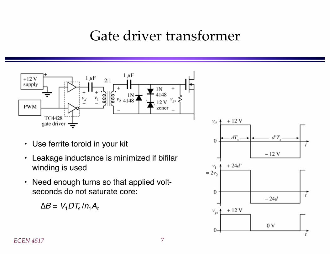
Gate driver transformer
• Use ferrite toroid in your kit• Leakage inductance is minimized if bifilar
winding is used
• Need enough turns so that applied volt-seconds do not saturate core:
∆B = V1DTs /n1Ac

ECEN 4517 8
Alternate smaller version of gate driver
• Uses only one gate driver instead of two, to produce half the voltage swing on primary
• Transformer turns ratio is 1:1• Produces half as much gate current• Suitable for smaller MOSFETs

ECEN 4517 9
Exp. 3, Part 1Test open-loop converter, outside
Basic control characteristics:How does the duty cycle control the PV and battery voltages and currents?

ECEN 4517 10
Prelab assignmentExp. 3, Part 1
Design your buck converter power stage1. Work out the current waveforms of each component: MOSFET,
diode, inductor, capacitors2. Design your inductor
• Use Kg method explained in ECEN 4797/5797• You decide how much ripple to allow, how much power loss to allow, etc.• Use one of the ferrite cores in your kit
3. Check the voltage and current stresses on each power component and make sure the components operate within their datasheet ratings
Contents of parts kit, with links to datasheets, is on web athttp://ecee.colorado.edu/~ecen4517/components/kit.html

ECEN 4517 11
Component stresses
Sketch the waveform for each power component and choose components that operate within their datasheet specified ratings:
MOSFETs: peak voltage, average currentDiodes: peak inverse voltage, average currentCapacitors: maximum working voltage, rms current
Most companies will apply derating factors to many of the datasheet limitsExample: 60% to 80% of datasheet max voltage value is
allowed for power semiconductors. This value includes worst-case peak transient voltages.
ECEN 4517 12
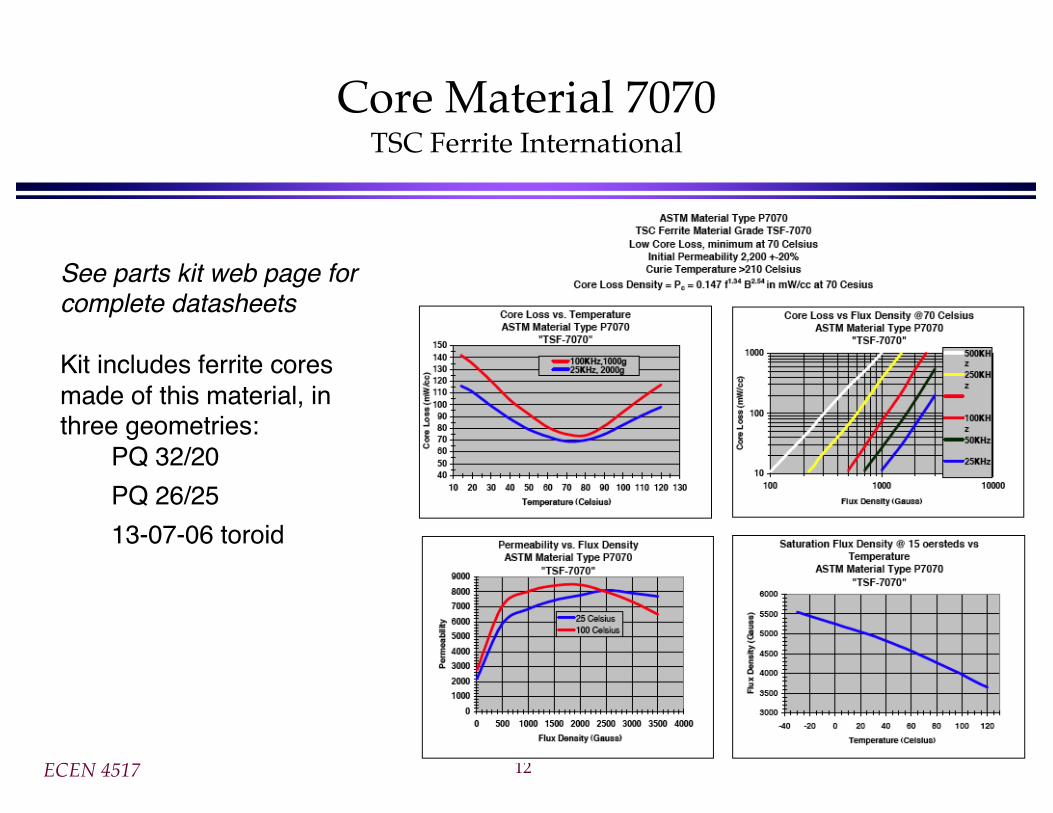
Core Material 7070TSC Ferrite International
See parts kit web page for complete datasheets
Kit includes ferrite cores made of this material, in three geometries:
PQ 32/20PQ 26/2513-07-06 toroid
ECEN 4517 13
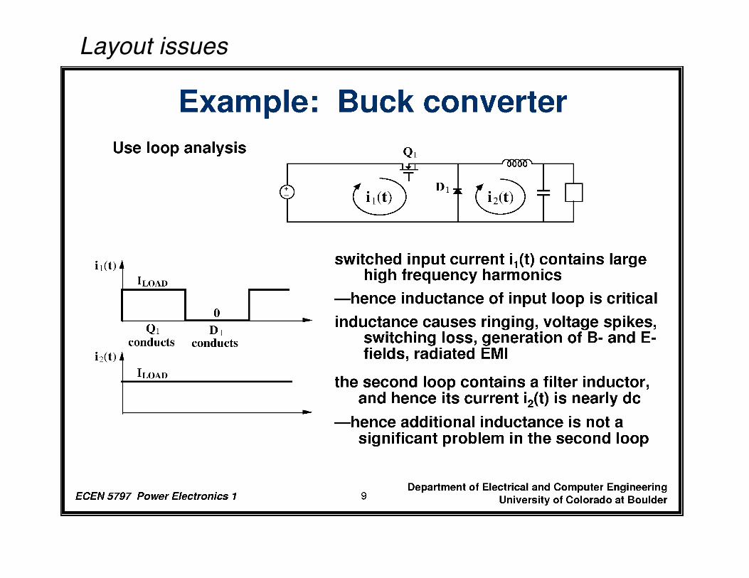
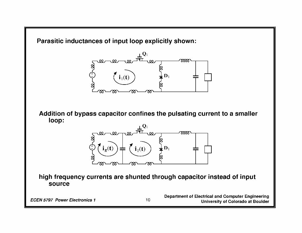
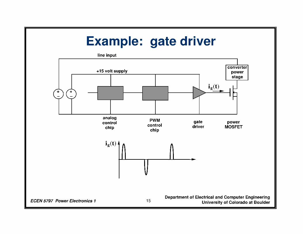
Layout issues
ECEN 4517 14

ECEN 4517 15
ECEN 4517 16

ECEN 4517 17
Top Related