


Languages
Pages
Legal

1
Lecture 7 1
Lecture 7
Electron mean free pathMicroscopy principles of SEM, TEM
Nanofabrication and Lithography
References:1) L. Reimer, “Scanning Electron Microscopy - Physics of Image Formation and Microanalysis”, 1985.2) R.E. Lee, “Scanning electron microscopy and X-Ray microanalysis, 1993.3) Woodruff & Delchar, Chapter 2 and pp. 449-460.4) Attard and Barnes, pp,25-28, 47-62.5) Kolasinski, pp.84-91, 107-108.6) LEEM: http://www.research.ibm.com/leem/#item2
7.1 Electron Mean Free Path
7.2 Scanning Electron Microscopy (SEM)
-SEM design; Secondary electron imaging; Backscattered electron Imaging7.3 Transmission Electron Microscopy (TEM)
- TEM/STEM design; spectroscopy (EELS)
7.4 Nanofabrication and Lithography
Lecture 7 2
Electron beam interactions with the sample
Lecture 7 3
7.1 Electron Scattering
Short inelastic mean free path for electrons means that elastic scattering of electrons is very surface sensitive
e
Electron diffraction and microscopy:
Elastic backscattered e-, ~ few % at 100eV
“Universal curve” for electrons
II: Interaction with plasmons
III: Inelastic electrons, Auger
IV: Secondary e-s, <50eV
2
Lecture 7 4
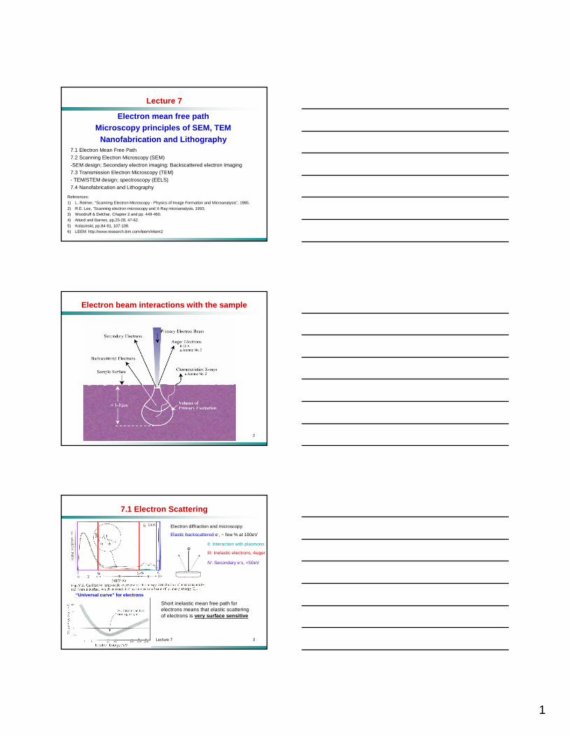
History of the Electron Microscope
1937: grad students J. Hillier and A. Prebus at U of Toronto built an electron microscope that magnified 7000x
1940 Hillier hired by RCA to build an electron microscope to sell (and pay back his salary!) (Electron microscope, U.S. Patent No. 2,354,263; 1944)
From Hillier’s patent
Lecture 7 5
7.2 Scanning Electron Microscopy (SEM)
Scanning electron microscopy (SEM)
- topology, morphology, chemical information (BSE and EDX)
• 0.5-1000keV electron energy
• field of view 0.1 - 100 µm
• 5 nm resolution in plane
• Magnification 10x – 300,000x• Typical operating pressure <1atms
• Non-destructive nature: though sometimes electron beam irradiation can cause sample damage
• Advantages : surface, common technique
• Disadvantages : vacuum compatibility; coating non-conductive specimens, typical cost: US$50,000 to 300,000
by Eric Barbagiovanni
Lecture 7 6
Electron beam-solid interactions
Backscattered electrons (BSEs) : are primary e’s leaving the specimen after a few large angle elastic scattering events
Secondary electrons (SEs) : are produced by the interactions between energetic e’s and weakly bonded valence e’s of the sample
Auger electron: incident e- kicks out an inner shell e-, a vacant e- state is formed; this inner shell vacant state is then filled by another e- from a higher shell, and simultaneously the energy is transferred to another e- that leaves the sample
Characteristic X-rays : emitted when a hole is created in the inner shell of an atom in the specimen due to inelastic e- scattering, as it can recombine with an outer shell e- (EDX)
Cathodoluminescene (CL) : light emission arising from the recombination of e-h pairs induced by excitation of e’s in the valence band during inelastic scattering in a semiconducting sample

3
Lecture 7 7
SEM/e-beam lithography in the Nanofab
The e-beam lithography system (right) is a LEO 1530 field emission scanning electron microscope (FE-SEM) fitted with a laser interferometer controlled stage (middle right).
The micrograph (bottom right) shows a square array of 300nm holes on 700nm pitch written in PMMA on Si. Also shown is an array of Cr dots on Si patterned by e-beam lithography and liftoff (below).
http://www.uwo.ca/fab/
Lecture 7 8
Schematic diagram of SEM
Filament (cathode) : free e’s by thermionic emission of W, LaB6
Wehnelt Cylinder: focuses the e-beam and stabilizes beam current
Anode Plate : maintains the HV difference between the anode and the cathode, and accelerates the free electrons down the column
Condenser Lens : reduces the diameter of the electron beam to produce a smaller spot size
Scan Coils: electromagnetically raster the e-beam on the surface
Final Objective Lens: focuses the e-beam on the surface; the smallest spot is about 5 nm (~ 1nm with a FI source)
Detectors : within the scope chamber, but not part of the column are the detectors
Lecture 7 9
Electron Sources: Thermionic Emission
• Richardson’s Equation : (derivation – aside)
Current density, j:
r = reflection coefficient;
• Richardson plot :
ln(j/T2) vs 1/T ⇒⇒ straight line
)exp()1( 2
kT
eTrAj o
φ−−=
223
2
deg4.120
4
cm
Amp
h
mekAo == π
Thermionic emission occurs when sufficient heat is supplied to the emitter so that e’s can overcome the work function, the energy barrier of the filament, Ew, and escape from it

4
Lecture 7 10
SEM Detectors
Everhart-Thornley (E-T) detectorEDX spectrometer
Lecture 7 11
Contrast of secondary electron micrograph
Contributions from (a) sample topography and (b) compositional contrast
Q: Why do the backscattered electron micrographs, rather than secondary electron micrographs reveal the compositional contrast?
Lecture 7 12
7.3 Transmission Electron Microscope (TEM)
Multipurpose machine!
Elastic scattering:• atomic structure (lattice parameters, orientation) (~1pm)
• microstructure and defects (~1nm-1µm) Inelastic scattering• Chemistry EDX (~ 1nm) and EELS
• Advantages : atomic resolution and depth resolution
• Disadvantages : difficult sample preparation, need UHV
• 100-3000keV electron energy
• resolution in plane 1nm (TEM) 0.6Å (HRTEM, current record)
http://videolectures.net/kolokviji_gloter_tem/http://www.ccmr.cornell.edu/igert/modular/docs/1_electron_microscopy.pdfhttp://www.rodenburg.org/RODENBURG.pdf
http://www.thebiotron.ca/modules-imaging.php
http://www.brockhouse.mcmaster.ca/facilities/tem.html
5
Lecture 7 13
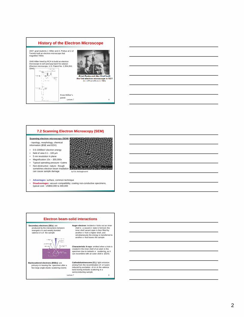
Inside HRTEM
Lecture 7 14
Sample preparation
Cross-section preparation (1-1.5 days)- gluing face-to-face
- cutting a slice
- mechanical polishing down to a thickness of 30µm- ion milling until perforation
FIB: a bit faster…
Lecture 7 15
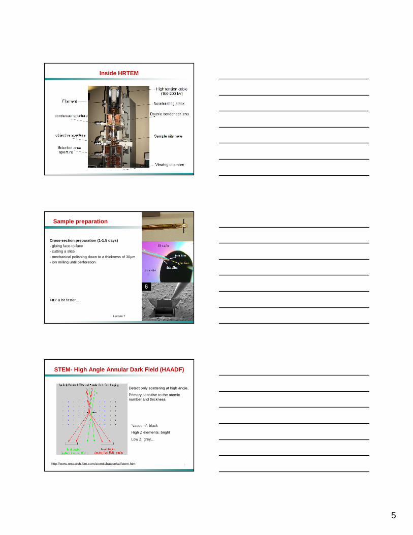
STEM- High Angle Annular Dark Field (HAADF)
http://www.research.ibm.com/atomic/batson/adfstem.htm
Detect only scattering at high angle,
Primary sensitive to the atomic number and thickness
“vacuum”: black
High Z elements: bright
Low Z: grey…
6
Lecture 7 16
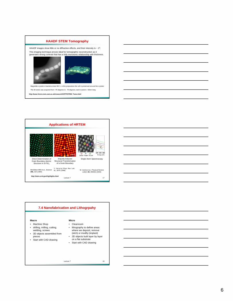
HAADF STEM Tomography
http://www-hrem.msm.cam.ac.uk/research/CETP/STEM_To mo.html
Magnetite crystals in bacteria strain MV-1, in this preparation the cell is preserved around the crystals.
The tilt series was acquired from +76 degrees to - 76 degrees; each crystal is ~60nm long.
HAADF images show little or no diffraction effects, and their intensity is ~ Z2.
This imaging technique proves ideal for tomographic reconstruction as it generates strong contrast that has a fully monotonic relationship with thickness.
Lecture 7 17
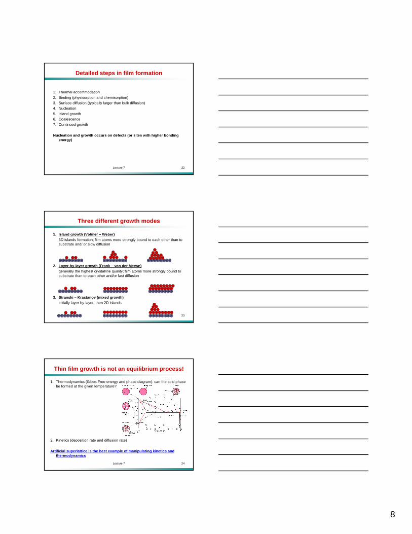
Applications of HRTEM
Impurity-Induced Structural Transformation
of a Grain Boundary
Y. Yan et al, Phys. Rev. Lett.81, 3675 (1998)
Direct Determination of Grain Boundary Atomic
Structure In SrTiO3
McGibbon MM et al., Science266, 102 (1994)
http://stem.ornl.gov/highlights.html
Single Atom Spectroscopy
M. Varela et al., Physical Review Letters 92, 095502 (2004)
Lecture 7 18
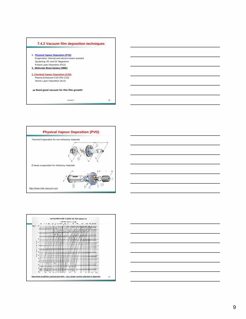
7.4 Nanofabrication and Lithogrpahy
Macro
• Machine Shop• drilling, milling, cutting,
welding, screws
• 3D objects assembled from pieces
• Start with CAD drawing
Micro
• Cleanroom• lithography to define areas
where we deposit, remove (etch) or modify (implant)
• 3D objects built layer by layer on a flat substrate
• Start with CAD drawing

7
Lecture 7 19
Cleanroom
Lecture 7 20
Lecture 7 21
7.4.1 Thermodynamics and kinetics of thin film grow th
What is a “thin film”?
How thin films are different from the bulk material s?Thin films may be:• Lower in density (compared to bulk analog)• Under stress• Different defect structures from bulk• Ultra-thin films (<10-20nm): quasi two dimensional• Strongly influenced by surface and interface effects
Steps in thin film growth• Separation of particles from source (heating, high voltage)• Transport• Condensation on substrate
8
Lecture 7 22
Detailed steps in film formation
1. Thermal accommodation
2. Binding (physisorption and chemisorption)
3. Surface diffusion (typically larger than bulk diffusion)
4. Nucleation5. Island growth
6. Coalescence
7. Continued growth
Nucleation and growth occurs on defects (or sites w ith higher bonding energy)
Lecture 7 23
Three different growth modes
1. Island growth (Volmer – Weber)3D islands formation; film atoms more strongly bound to each other than to substrate and/ or slow diffusion
2. Layer-by-layer growth (Frank – van der Merwe)generally the highest crystalline quality; film atoms more strongly bound to substrate than to each other and/or fast diffusion
3. Stranski – Krastanov (mixed growth)initially layer-by-layer, then 2D islands
Lecture 7 24
Thin film growth is not an equilibrium process!
1. Thermodynamics (Gibbs Free energy and phase diagram): can the sold phase be formed at the given temperature?
2. Kinetics (deposition rate and diffusion rate)
Artificial superlattice is the best example of manip ulating kinetics and thermodynamics
9
Lecture 7 25
7.4.2 Vacuum film deposition techniques
1. Physical Vapour Deposition (PVD)Evaporation: thermal and electron-beam assisted
Sputtering: RF and DC Magnetron
Pulsed Laser Deposition (PLD)3. Molecular Beam Epitaxy (MBE)
2. Chemical Vapour Deposition (CVD)Plasma-Enhanced CVD (PE-CVD)Atomic Layer Deposition (ALD)
⇒⇒⇒⇒ Need good vacuum for thin film growth!
Lecture 7 26
Physical Vapour Deposition (PVD)
Thermal Evaporation for non-refractory materials
E-beam evaporation for refractory materials
http://www.mdc-vacuum.com
Lecture 7 27http://www.mcallister.com/vacuum.html – see a larger version attached in Appendix

10
Lecture 7 28
Sputtering Deposition
• DC for conducting materials
• RF for insulating materialsMagnetron sputtering is most popular due to high rate and low operation
pressure
Lecture 7 29
Pulsed Laser Deposition (PLD)
• Good for multielemental materials (P < 1 Torr)
Lecture 7 30
Molecular Beam Epitaxy (MBE)
Molecular Beam Epitaxy
(p < 10-8Torr)
1. Elemental Superlattices: Giant Magneto-Resistiance (GMR) Devices
2. Binary III-V Superlattices
3. Complex Oxide Superlattices
11
Lecture 7 31
Complex oxides are not that complex:
Most of them are based on the ABO3 cubic perovskite structure
Ex.:: SrTiO3, LaTiO3, LaMnO3, LaAlO3, …
⇒ Favorable to atomically smooth layered heterostructures
ABO3A: M2+ (Ca, Sr, Ba, La)B: M4+ (Ti, Zr, Mn)
Lecture 7 32
Superlattices grown by MBE
M. Warusawithana, J. Zuo, H. Chen and J. N. Eckstein
A. Ohtomo, H. Y. Hwang, Nature 419, 378 (2002)
LaTiO 3/SrTiO 3 (PLD)SrTiO 3/BaTiO 3/CaTiO3
Lecture 7 33
Epitaxial oxide material integrated with Si
5nm
Si
SrTiO3
Epitaxial vs amorphous or polycrystalline1. Sc2O3/Si(111)
2. SrTiO3/Si(001)
• Epitaxial structures may afford controllable interfaces (no dangling bonds…)• Demonstration of interface stability and identification of potential stability problems under oxidizing/reducing conditions
SrTiOSi
?
12
Lecture 7 34
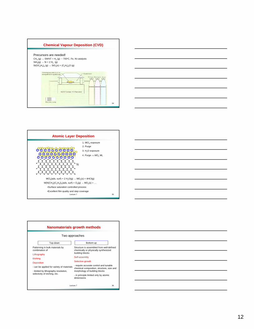
Chemical Vapour Deposition (CVD)
Precursors are needed!CH4 (g) → SWNT + H2 (g) ~ 700oC, Fe, Ni catalysts
SiH4(g) → Si + 2 H2 (g)
Si(OC2H5)4 (g) → SiO2(s) + (C2H5)2O (g)
Lecture 7 35
Atomic Layer Deposition
MCl4(ads, surf) + 2 H2O(g) → MO2(s) + 4HCl(g)
M(N(CH3)(C2H5))4(ads, surf) + O3(g) → MO2(s) + …
•Surface saturation controlled process
•Excellent film quality and step coverage
1. MCl4 exposure
2. Purge
3. H2O exposureHCl
H2O
4. Purge ⇒ MO2 ML
Si
Lecture 7 36
Nanomaterials growth methods
Two approaches
Top-down Bottom-up
Patterning in bulk materials by combination of
Lithography
Etching
Deposition
- can be applied for variety of materials
- limited by lithography resolution, selectivity of etching, etc.
Structure is assembled from well-defined chemically or physically synthesized building blocks
Self-assembly
Selective growth
- require accurate control and tunable chemical composition, structure, size and morphology of building blocks
- in principle limited only by atomic dimensions

13
Lecture 7 37
Mechanical Methods (Mechanosynthesis)
Low cost fabrication: ball milling or shaker milling
Kinetic energy from a rotating or vibrating canister is imparted to hard spherical ball bearings (under controlled atmosphere)
(1) Compaction and rearrangement of particles
(2) First elastic and then severe plastic deformation of the sample material ⇒ formation of defects and dislocations
(3) Particle fracture and fragmentation with continuous size reduction ⇒ formation of nanograined material
σF – stress level, when crack propagation leads to fracture; γ - surface energy of the particle; a - length of a crack
-material with defects with a wide distribution of size
aYK FIC πσ=a
E
a
K
YIC
F
γσ ~1
~
Lecture 7 38
High-Energy Methods: Discharge Plasma Method
Application of high energy electric current (monochromatic radiation – laser ablation)
Can be used for fullerenes and C nanotubes
Process depend on:
-Pressure of He, process temperature, applied current
final product requires extensive purification
Lecture 7 39
Chemical Fabrication Methods
Anodizing (and electropolishing)
Insulating porous oxide layer is created on a conductive metal anode in electrolytic solution
Porous Al2O3 membranes can be considered as ultimate template material
Anodic reaction 2Al0(s) → 2 Al3+ + 6e
Oxide-electrolyte interface 2 Al3+ + 3H2O → 2 Al2O3 + 6H+
Cathodic reaction 6H+ + 6e → 3 H2 (g)
Overall oxide formation reaction:
2Al0(s) + 3H2O → Al2O3 + 3 H2

14
Lecture 7 40
Lithographic Methods
Lecture 7 41
Top-bottom: High-Aspect Aspect-Ratio Si Structures
nanotextured Si surface dense silicon pillar array
Lecture 7 42
Bottom-up: vapor-liquid-solid growth
• Metal particle catalyzed the decomposition of a gaseous species containing the semiconductor components, e.g. Ge, or Ga and As
• Metal catalyst particles absorb species, becoming saturated with them at eutectic point (relatively low temperature)
• When semiconductor reaches supersaturation, it precipitates out of the eutectic
• Metal prepared and deposited/grown on surface
• Metal droplet size determines eventual wire diameter
VLS growth of Ge NWsw/Au (from E. Garfunkel)

15
Lecture 7 43
Cartoon of growth
Metallic catalyst
nanocluster
Eutectic (AuGe alloy)Temperature is
controlled to keep it in the liquid state
Nanowirenucleation begins
when the liquid become saturated
with Ge
Nanowire growthcontinues as long
as Au-Ge alloy stays liquid and Ge
concentration is high enough
Lecture 7 44
Electrochemical step decoration
- minimization surface energy of the step- metal oxide electrochemical deposition + reduction (H2)- metal electrochemical deposition
Lecture 7 45
Designed Synthesis of Hierarchical Structures
The evolution of nanowire structural and compositional complexity enabled today by controlled synthesis
(a) from homogeneous materials(b) axial and radial heterostructures(c) branched heterostructures
The colors indicate regions with distinct chemical composition and/or doping
16
Lecture 7 46
Organization and Assembly of Nanowires
Using a patterned catalyst, NWs can be directly grown on a solid substrate in a designed configuration
NW materials produced under synthetic conditions optimized for their growth can be organized into arrays by several techniques
(1) electric - field – directed (highly anisotropic structures and large polarization)
(2) fluidic - flow – directed (passing a suspension of NWs through microfluidicchannel structure)
(3) Langmuir–Blodgett (ordered monolayer is formed on water and transferred to a substrate)
(4) patterned chemical assembly or imprint
Lecture 7 47
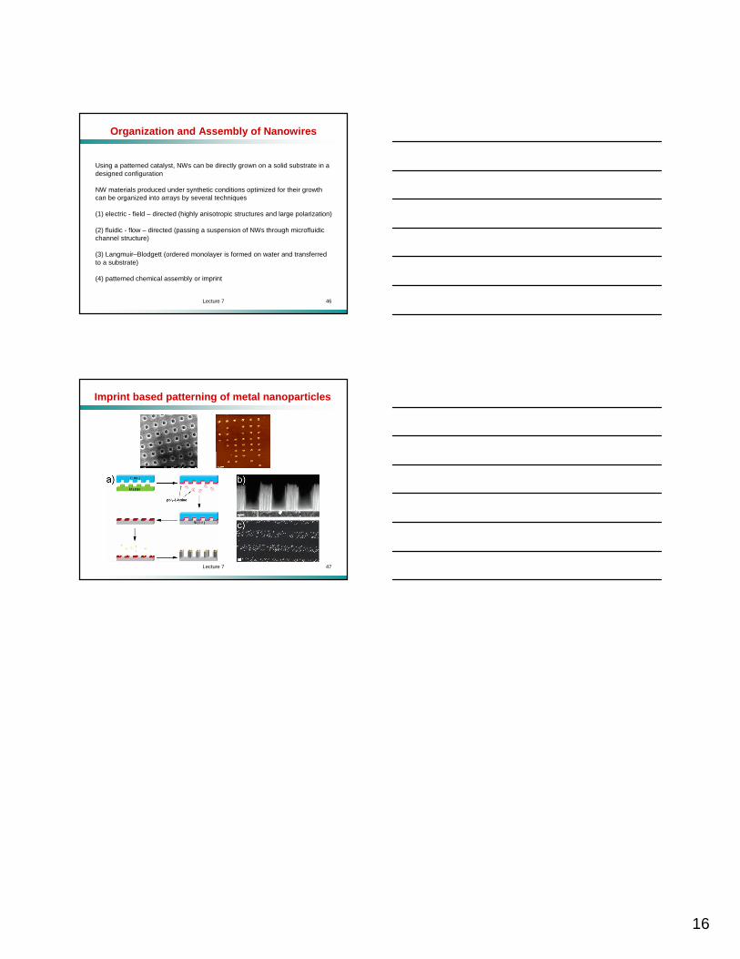
Imprint based patterning of metal nanoparticles
Top Related