Chapter 9 Electron mean free path Microscopy principles...
10
1 Chapter 9 1 Chapter 9 Electron mean free path Microscopy principles of SEM, TEM, LEEM References: 1) L. Reimer, “Scanning Electron Microscopy - Physics of Image Formation and Microanalysis”, 1985. 2) R.E. Lee, “Scanning electron microscopy and X-Ray microanalysis, 1993 3) D.P. Woodruff, T.A. Delchar, “Modern Techniques of Surface Science”, Chapter 2 and pp. 449-460 4) K. Kolasinski, “Surface Science: Foundations of Catalysis and Nanoscience. 2nd ed.; Wiley & Sons, 2008; pp.84-91, 107-108 5) LEEM: http://www.research.ibm.com/leem/#item2 9.1 Electron Mean Free Path 9.2 Scanning Electron Microscopy (SEM) -SEM design; Secondary electron imaging; Backscattered electron Imaging 9.3 Transmission Electron Microscopy (TEM) - TEM/STEM design; High Angle Annular Dark Field (HAADF) 9.4 Low Energy Electron Microscopy (LEEM) Chapter 9 2 Electron beam interactions with the sample
Transcript of Chapter 9 Electron mean free path Microscopy principles...

1
Chapter 9 1
Chapter 9
Electron mean free pathMicroscopy principles of SEM, TEM, LEEM
References:
1) L. Reimer, “Scanning Electron Microscopy - Physics of Image Formation and Microanalysis”, 1985.
2) R.E. Lee, “Scanning electron microscopy and X-Ray microanalysis, 1993
3) D.P. Woodruff, T.A. Delchar, “Modern Techniques of Surface Science”, Chapter 2 and pp. 449-460
4) K. Kolasinski, “Surface Science: Foundations of Catalysis and Nanoscience. 2nd ed.; Wiley & Sons, 2008; pp.84-91, 107-108
5) LEEM: http://www.research.ibm.com/leem/#item2
9.1 Electron Mean Free Path9.2 Scanning Electron Microscopy (SEM)-SEM design; Secondary electron imaging; Backscattered electron Imaging
9.3 Transmission Electron Microscopy (TEM)- TEM/STEM design; High Angle Annular Dark Field (HAADF) 9.4 Low Energy Electron Microscopy (LEEM)
Chapter 9 2
Electron beam interactions with the sample
2
Chapter 9 3
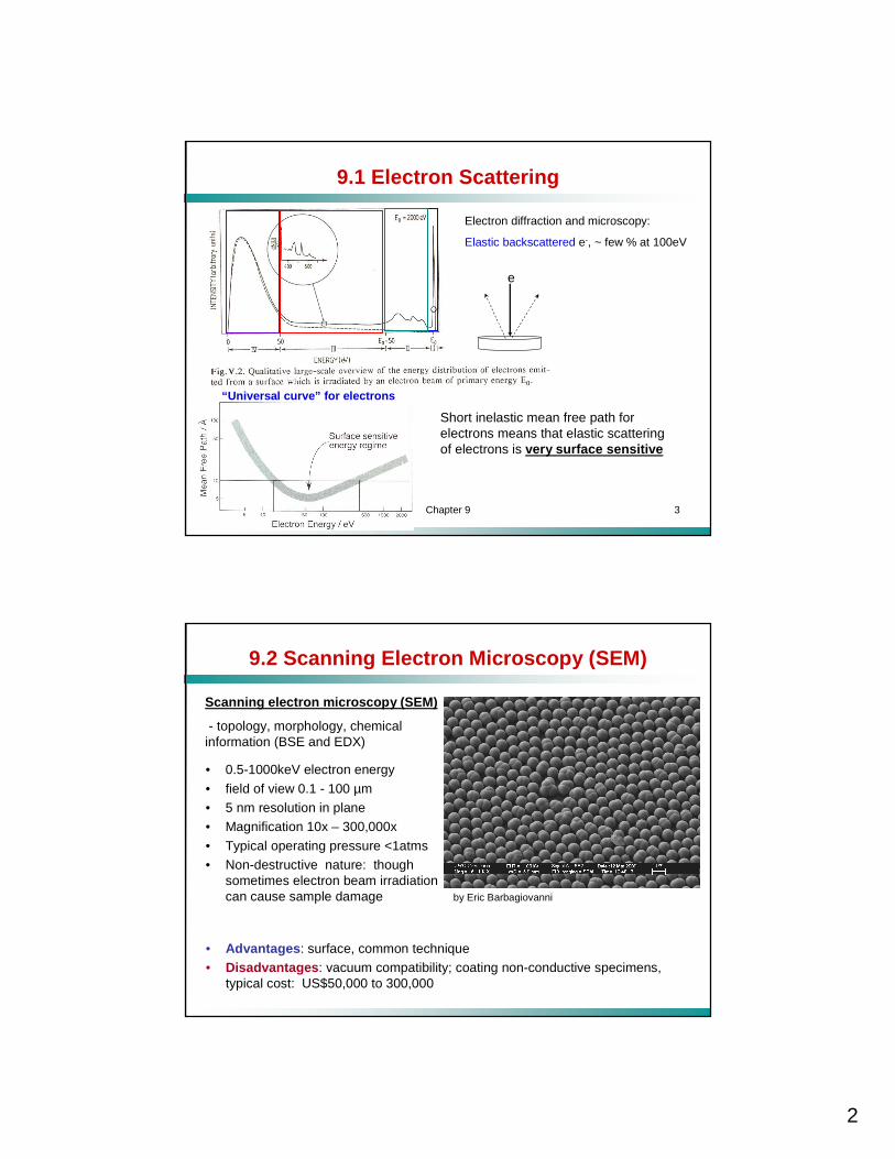
9.1 Electron Scattering
Short inelastic mean free path for electrons means that elastic scattering of electrons is very surface sensitive
e
Electron diffraction and microscopy:
Elastic backscattered e-, ~ few % at 100eV
“Universal curve” for electrons
Chapter 9 4
9.2 Scanning Electron Microscopy (SEM)
Scanning electron microscopy (SEM)
- topology, morphology, chemical information (BSE and EDX)
• 0.5-1000keV electron energy
• field of view 0.1 - 100 µm• 5 nm resolution in plane• Magnification 10x – 300,000x
• Typical operating pressure <1atms• Non-destructive nature: though
sometimes electron beam irradiation can cause sample damage
• Advantages : surface, common technique• Disadvantages : vacuum compatibility; coating non-conductive specimens,
typical cost: US$50,000 to 300,000
by Eric Barbagiovanni

3
Chapter 9 5
Electron beam solid interaction
Backscattered electrons (BSEs) : are primary e’s leaving the specimen after a few large angle elastic scattering events
Secondary electrons (SEs) : are produced by the interactions between energetic e’s and weakly bonded valence e’s of the sample
Auger electron: incident e- kicks out an inner shell e-, a vacant e- state is formed; this inner shell vacant state is then filled by another e- from a higher shell, and simultaneously the energy is transferred to another e- that leaves the sample
Characteristic X-rays : emitted when a hole is created in the inner shell of an atom in the specimen due to inelastic e- scattering, as it can recombine with an outer shell e- (EDX)
Cathodoluminescene (CL) : light emission arising from the recombination of e-h pairs induced by excitation of e’s in the valence band during inelastic scattering in a semiconducting sample
Chapter 9 6
SEM/e-beam lithography in the Nanofab
The e-beam lithography system (right) is a LEO 1530 field emission scanning electron microscope (FE-SEM) fitted with a laser interferometer controlled stage (middle right).
The micrograph (bottom right) shows a square array of 300nm holes on 700nm pitch written in PMMA on Si. Also shown is an array of Cr dots on Si patterned by e-beam lithography and liftoff (below).
http://www.uwo.ca/fab/
4
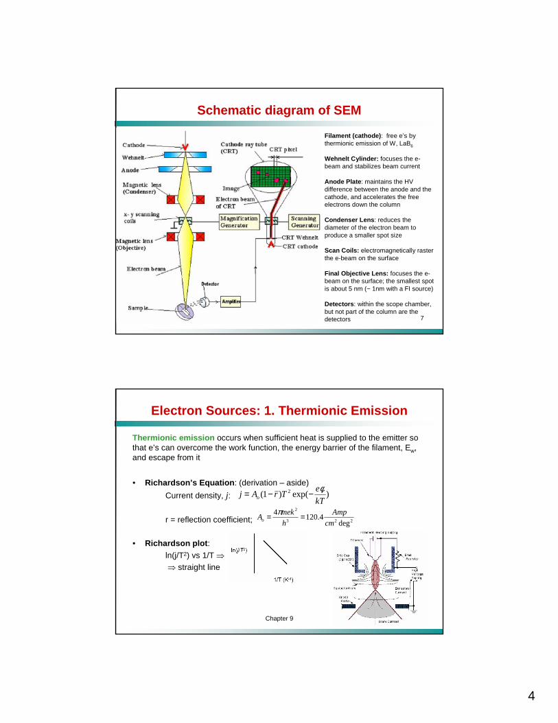
Chapter 9 7
Schematic diagram of SEM
Filament (cathode) : free e’s by thermionic emission of W, LaB6
Wehnelt Cylinder: focuses the e-beam and stabilizes beam current
Anode Plate : maintains the HV difference between the anode and the cathode, and accelerates the free electrons down the column
Condenser Lens : reduces the diameter of the electron beam to produce a smaller spot size
Scan Coils: electromagnetically raster the e-beam on the surface
Final Objective Lens: focuses the e-beam on the surface; the smallest spot is about 5 nm (~ 1nm with a FI source)
Detectors : within the scope chamber, but not part of the column are the detectors
Chapter 9 8
Electron Sources: 1. Thermionic Emission
• Richardson’s Equation : (derivation – aside)
Current density, j:
r = reflection coefficient;
• Richardson plot :
ln(j/T2) vs 1/T ⇒⇒ straight line
)exp()1( 2
kT
eTrAj o
φ−−=
223
2
deg4.120
4
cm
Amp
h
mekAo == π
Thermionic emission occurs when sufficient heat is supplied to the emitter so that e’s can overcome the work function, the energy barrier of the filament, Ew, and escape from it

5
Chapter 9 9
Field Electron Emission
• Electron tunneling through low, thin barrier
– Field emission, when F>3×10⁷ V/cm ~ 0.3 V/Å• General relation for electron emission in high field:
• P is given by WKB approximation
• If approximate barrier by triangle:
• Fowler – Nordheim eqn, including potential barrier:
ZZZ dEEvFEPej )(),(0∫∞
=
−−×= ∫
l
Z dzEVm
constP0
2/12/13/2
)(2
exph
FF
2/32/1
2
1~
2
1~
φφφ∫
−×=
F
mconstP
2/32/13/22exp
φh
φφ
φ
2/12/32/372
26 where;
)(1083.6exp)(1054.1
Fey
F
yfyt
Fj =
×−×= −
Chapter 9 10
SEM Detectors
Everhart-Thornley (E-T) detector EDX spectrometer
6
Chapter 9 11
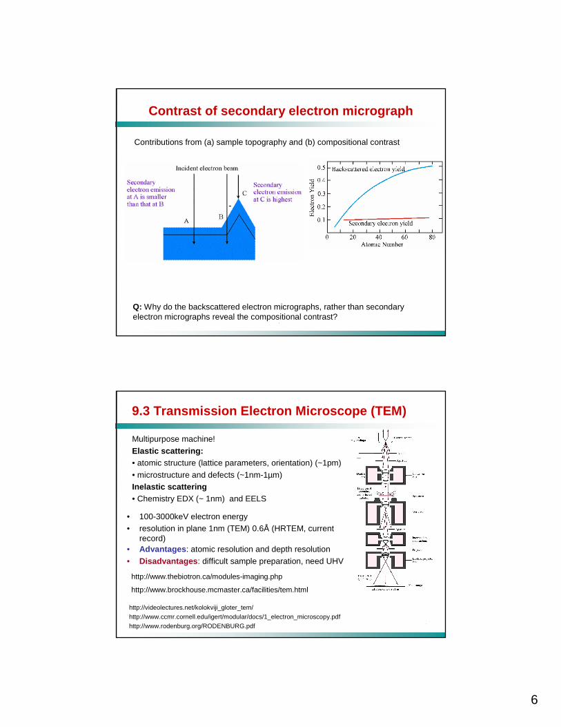
Contrast of secondary electron micrograph
Contributions from (a) sample topography and (b) compositional contrast
Q: Why do the backscattered electron micrographs, rather than secondary electron micrographs reveal the compositional contrast?
Chapter 9 12
9.3 Transmission Electron Microscope (TEM)
Multipurpose machine!
Elastic scattering:• atomic structure (lattice parameters, orientation) (~1pm)
• microstructure and defects (~1nm-1µm) Inelastic scattering• Chemistry EDX (~ 1nm) and EELS
• Advantages : atomic resolution and depth resolution
• Disadvantages : difficult sample preparation, need UHV
• 100-3000keV electron energy• resolution in plane 1nm (TEM) 0.6Å (HRTEM, current
record)
http://videolectures.net/kolokviji_gloter_tem/
http://www.ccmr.cornell.edu/igert/modular/docs/1_electron_microscopy.pdf
http://www.rodenburg.org/RODENBURG.pdf
http://www.thebiotron.ca/modules-imaging.php
http://www.brockhouse.mcmaster.ca/facilities/tem.html

7
Chapter 9 13
Sample preparation
Cross-section preparation (1-1.5 days)- gluing face-to-face- cutting a slice
- mechanical polishing down to a thickness of 30µm- ion milling until perforation
FIB (see Appendix I): a bit faster…
Chapter 9 14
STEM- High Angle Annular Dark Field (HAADF)
http://www.research.ibm.com/atomic/batson/adfstem.htm
Detect only scattering at high angle, primary sensitive to the atomic number and thickness
“vacuum”: black
High Z elements: bright
Low Z: grey…

8
Chapter 9 15
HAADF STEM Tomography
http://www-hrem.msm.cam.ac.uk/research/CETP/STEM_Tomo.html
Magnetite crystals in bacteria strain MV-1, in this preperation the cell is preserved around the crystals.
The tilt series was acquired from +76 degrees to - 76 degrees; each crystal is ~60nm long.
HAADF images show little or no diffraction effects, and their intensity is ~ Z2.
This imaging technique proves ideal for tomographic reconstruction as it generates strong contrast that has a fully monotonic relationship with thickness.
Chapter 9 16
Applications of HRTEM
Impurity-Induced Structural Transformation
of a Grain Boundary
Y. Yan et al, Phys. Rev. Lett.81, 3675 (1998)
Direct Determination of Grain Boundary Atomic
Structure In SrTiO3
McGibbon MM et al., Science266, 102 (1994)
http://stem.ornl.gov/highlights.html
Single Atom Spectroscopy
M. Varela et al., Physical Review Letters 92, 095502 (2004)
9
Chapter 9 17
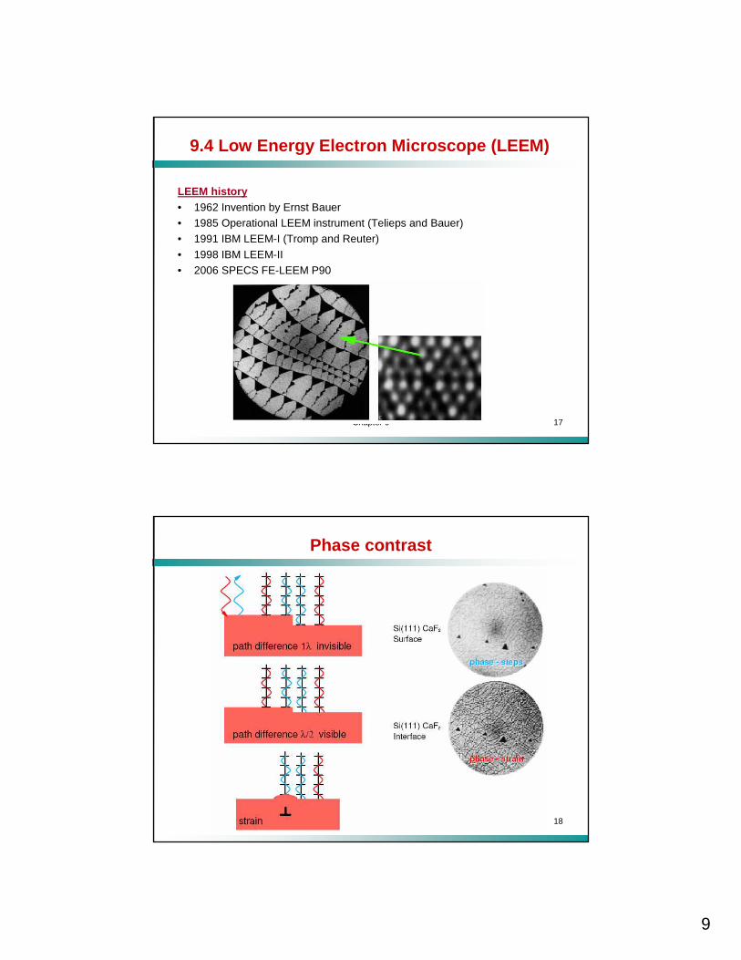
9.4 Low Energy Electron Microscope (LEEM)
LEEM history• 1962 Invention by Ernst Bauer• 1985 Operational LEEM instrument (Telieps and Bauer)• 1991 IBM LEEM-I (Tromp and Reuter)
• 1998 IBM LEEM-II• 2006 SPECS FE-LEEM P90
Chapter 9 18
Phase contrast

10
Chapter 9 19
IBM LEEM II
Surf. Reviews and Lett. 5 (1998) 1189
After diffraction, electrons are accelerated from ~ 1 eV to ~ 10,000 eV
Chapter 9 20
LEEM operating parameters
• 0 - 100 eV electron energy• field of view 1 - 100 µm
• 5 nm resolution in plane• vertical resolution: atomic steps, 0.1 nm• in situ growth, etching
• RT – 1200oC
⇒ extremely useful tool to study crystal growth in situ
* From R.M Tromp