


Languages
Pages
Legal


Development of a Hardware and Software Redundant Cube Satellite Flight Computer
by
Steven Richard Peeples
A thesis submitted to the Graduate Faculty of
Auburn University
in partial fulfillment of the
requirements for the Degree of
Master of Science
Auburn, Alabama
August 4, 2018
Keywords: fault-tolerant, flight computer, cube satellite,
robust computing, fault recovery
Copyright 2018 by Steven Peeples
Approved by
Dr. Sanjeev Baskiyar, Chair, Professor of Computer Science & Software Engineering
Dr. Bhattacharya, Assistant Professor of Computer Science & Software Engineering
Dr. Zhou, Assistant Professor of Computer Science & Software Engineering

ii
Abstract
Flight computers (FCs) for cube satellites, or cubeSats, have been unreliable in the harsh
environment of space. Radiation single event effects (SEE) and total ionization dose (TID) cause
significant failure in spacecraft. Radiation hardened parts can reduce the probability of failure
but are two orders of magnitude more costly than commercial parts, placing them beyond the
budget of most cubeSat missions. A commonly used alternate method is to use commercial parts
and redundancy. Past work in this area offers robustness but is still vulnerable to system-wide
failure. The proposed system, the Quatara flight computer system, improves upon past work
using three redundant strings of processing elements with majority voting to operate and control
a satellite. Although the system requires FC software, the focus of this work is the hardware
architecture and FPGA algorithms. The Quatara flight computer system is a recoverable,
redundant, single fault-tolerant system with increased robustness for cubeSats to serve low-cost,
big data missions for NASA, Department of Defense (DoD), industry, and universities. It
contains no proprietary components or software, making alterability and updateability relatively
simple.

iii
Table of Contents
Chapter 1 Introduction ............................................................................................................... 1
1.1 Single Event Effects ......................................................................................................... 3
1.2 Total Ionizing Dose .......................................................................................................... 4
1.3 Field Programmable Gate Arrays ..................................................................................... 4
1.4 Triple Modular Redundancy ............................................................................................ 6
1.5 Related Work.................................................................................................................... 7
1.5.1 TREMOR .................................................................................................................. 7
1.5.2 RadSat ....................................................................................................................... 8
1.5.3 Dependable Multiprocessor (DM) ............................................................................ 9
1.6 Summary .......................................................................................................................... 9
1.7 Goals............................................................................................................................... 11
Chapter 2 Architecture............................................................................................................. 12
Chapter 3 Hardware ................................................................................................................. 18
Chapter 4 Algorithms .............................................................................................................. 25
Chapter 5 Testing..................................................................................................................... 47
5.1 PPS Period ...................................................................................................................... 47
5.2 Synchronization Accuracy ............................................................................................. 49

iv
5.3 Interruption of Normal Start Sequence .......................................................................... 51
5.4 Random String Reset ...................................................................................................... 52
5.5 Voting Logic .................................................................................................................. 53
Chapter 6 Flight Computer ...................................................................................................... 59
Chapter 7 Conclusion .............................................................................................................. 62
Chapter 8 Future Work ............................................................................................................ 63
Chapter 9 Bibliography ........................................................................................................... 64

v
List of Tables
Table 1 ProASIC3 Compile Report – No TMR............................................................................ 21
Table 2 ProASIC3 Compile Report – C-C ................................................................................... 22
Table 3 ProASIC3 Compile Report – TMR ................................................................................. 23
Table 4 Propagation Comparison.................................................................................................. 23
Table 5 Period Test Data............................................................................................................... 48
Table 6 Synchronization Accuracy Test Data .............................................................................. 50
Table 7 Maximum Divergence on Reset Test Data ...................................................................... 53

vi
List of Figures
Figure 1 Basic Architecture ............................................................................................................ 2
Figure 2 FPGA Internal Block Diagram ......................................................................................... 5
Figure 3 TMR Voter ....................................................................................................................... 7
Figure 4 TREMOR Flight Computer Block Diagram .................................................................... 8
Figure 5 RadSat Flight Computer ................................................................................................... 8
Figure 6 DM Payload Processing Architecture .............................................................................. 9
Figure 7 String Hardware .............................................................................................................. 13
Figure 8 FPGA to FPGA Communication .................................................................................... 14
Figure 9 Data Transfer .................................................................................................................. 15
Figure 10 Block Data .................................................................................................................... 16
Figure 11 Data Transfer Windows ................................................................................................ 17
Figure 12 Breadboard Prototype ................................................................................................... 18
Figure 13 PCB Prototype .............................................................................................................. 19
Figure 14 FPGA Code Block Diagram ......................................................................................... 26
Figure 15 FPGA Code Block Diagram for Synchronization Control ........................................... 27
Figure 16 Synchronization Timing ............................................................................................... 28
Figure 17 Pulse Detector Flow Diagram ...................................................................................... 29
Figure 18 Pseudocode for Pulse Detector Algorithm ................................................................... 31
Figure 19 Pseudocode for PID Algorithm .................................................................................... 32
Figure 20 Sync Flow Diagram ...................................................................................................... 34

vii
Figure 21 Pseudocode for Sync Algorithm ................................................................................... 36
Figure 22 Primary Behavior Flow Diagram ................................................................................. 38
Figure 23 Pseudocode for Primary Behavior Sync Algorithm ..................................................... 39
Figure 24 Secondary Behavior Flow Diagram ............................................................................. 41
Figure 25 Pseudocode for Secondary Behavior Sync Algorithm ................................................. 43
Figure 26 Tertiary Behavior Flow Diagram ................................................................................. 44
Figure 27 Pseudocode for Tertiary Behavior ................................................................................ 46
Figure 28 PPS Period Measurement ............................................................................................. 47
Figure 29 PPS Synchronization Accuracy .................................................................................... 49
Figure 30 Synchronization Accuracy Testing............................................................................... 50
Figure 31 Maximum Divergence on Restart ................................................................................. 52
Figure 32 Voting Logic Test Setup ............................................................................................... 54
Figure 33 Voting Logic Test Hardware ........................................................................................ 54
Figure 34 Voting Logic Test1 ....................................................................................................... 55
Figure 35 Voting Logic Test2 ....................................................................................................... 55
Figure 36 Voting Logic Test3 ....................................................................................................... 56
Figure 37 Voting Logic Test4 ....................................................................................................... 56
Figure 38 Voting Logic Test5 ....................................................................................................... 57
Figure 39 Voting Logic Test6 ....................................................................................................... 57
Figure 40 FC Software Flow Diagram.......................................................................................... 60

viii
List of Abbreviations
ALU Arithmetic Logic Unit
CMOS Complementary Metal-Oxide-Semiconductor
COTS Commercial Off The Shelf
DM Dependable Multiprocessor
DoD Department of Defense
FC Flight Computer
FCR Fault Containment Region
FPGA Field Programmable Gate Array
HDL Hardware Description Language
IC Integrated Circuit
LED Light-Emitting Diode
LEO Low Earth Orbit
PCB Printed Circuit Board
PID Proportional Integral Derivative
PPS Pulse Per Second
SEE Singe Event Effects
SEL Single Event Latch
SEU Single Event Upset
SPI Serial Peripheral Interface

ix
SRAM Static Random Access Memory
TID Total Ionization Dose
TMR Triple Modular Redundancy
TREMOR TRiplE MOdular Redundant Flight Computer
UART Universal Asynchronous Receiver-Transmitter

1
Chapter 1 Introduction
Cube Satellites are a class of small, low-cost satellites. Due to the size/mass limitations of the
satellites, little redundancy is allowed to increase the robustness and thus the quality of science
returned from missions. Space is an unforgiving wasteland to operate in. Radiation, single event
effects (SEEs), temperature swings, as well as limits on power, heat dissipation and
communication make flight computers react unreliably. Nearly half of all cubeSats launched fail
to function [1]. Two common methods are used to increase robustness: single string radiation
hardened parts or multi-string redundant hardware schemes. The focus of this thesis is the latter.
Radiation hardened parts are expensive and lack the performance of today’s commercial
components [2]. In fact, radiation hardened parts are two orders of magnitude more expensive [3]
[4] than commercial ones and delivery lead time is commonly six months [5] [6] or more.
Commercial electronic components continue to become smaller, faster and more power efficient
than their radiation hardened counterparts. Flying COTS in space is a long-held desire of DoD and
NASA [7]. Even in triples, the cost and size are much smaller than radiation hardened components.
The comparatively small market for radiation parts limits their evolution. The Quatara flight
computer uses three redundant strings of single board computers with a majority voting scheme to
operate and control a satellite. The basic architecture is an “E” configuration. The block diagram
is shown Figure 1.

2
FC1 FC2 FC3
FPGA1 FPGA2 FPGA3
String 1 String 2 String 3
Figure 1 Basic Architecture
In the proposed scheme, the flight computers each transfer input information to an external
memory (inside the FPGA). Next, the FPGA transmits the data to the other FPGAs as well and
receiving and storing other FPGAs’ transmitted data. The FC is notified that the process is
complete and can access data from all three FCs in the memory. The entire set of data is compared
and voted upon. Erroneous data is discarded and a hardware reboot of that string (the entire
redundant element) is initiated to attempt recovery. A power cycle clears any type of single event
upset (SEU) or single event latchup (SEL) [8]. While it is possible for the FCs to interchange data
directly, FPGAs are used in this system to reduce overhead and to accurately control timing and
synchronization. From the FC’s perspective, once the local data is saved, other FCs’ local data
appears in memory with it a short time later.
The proposed system consists of a redundant FC only. A truly redundant spacecraft would require
backup power, instrumentation, and effectors, e.g. thrusters and reaction wheels, but such is not
possible given the mass and space constraints of cubeSats. Even with non-redundant element

3
failure and a healthy FC, telemetry may still be able to be sent to ground control about the problem
so workarounds can be initiated. The key is to maintain control of the spacecraft. Graceful
degradation is preferred over total loss.
The state vector is updated and shared continuously so when the primary FC goes down or is forced
to restart, seamless transfer of control can occur to backups. Restarted FCs receive the “live” state
vector and can resume where they left off.
1.1 Single Event Effects
SEEs are anomalies in electronics caused by energetic particles in space radiation [2] [8] [9]. These
effects are typically not seen on the earth’s surface due to our magnetosphere. Various types of
SEE exist, but the most common is SEU and SEL [10]. In an SEU, an energetic particle travels
through a P-N junction in such a way as to cause electron-hole pairs to form resulting in temporary
current flow across the junction. If the flow is high enough it will cause a bit flip, corrupting data
[8] [9]. In an SEL, the particle travels through a NAND gate causing a self-amplifying short circuit
to occur. This causes increased power consumption, heat dissipation, and possibly permanent
damage to the digital circuit [8] [9] [11]. For complementary metal-oxide-semiconductor (CMOS)
integrated circuits (IC)s, which is a common manufacturing technology, SELs are a common cause
of failure and many space systems cannot tolerate even one of them [12]. The most important
attribute of latchup and SEL in particular is that the latched state can only be released by turning
off the device [10] [11] [12]. Statistics have shown that at 380km, which is in the range of low

4
earth orbit (LEO), SEEs can be expected at a rate of one every 15 minutes on average in a typical
flight computer [9].
1.2 Total Ionizing Dose
The total ionizing dose (TID) is the measure of the cumulative ionizing radiation that electronics
receive over a period of time [13] [10]. In LEO the main source of radiation is from the Van Allen
Radiation belts surrounding the earth [14]. The common unit is krad(Si) which equals 103 rad(Si)
or 10 milligray where the parenthetical represents the material, silicon [10]. Radiation accelerates
the aging of electronic parts and can lead to degradation of electrical performance [15]. At doses
higher than 20 krad switching speed is affected and finally the device fails to function [10].
Redundancy is an effective technique for tolerating total ionizing dose [16].
1.3 Field Programmable Gate Arrays
An FPGA is a general purpose digital device that implements digital logic however the designer
wants [17] [18] [19]. Standard “off-the-shelf” ICs have a fixed, predesigned circuit operation from
the manufacturer; an FPGA does not. Its function is designed by the end user for a particular
application. It can be reconfigured as many times as needed [18]. An FPGA is completely
manufactured but remains design independent. Internal switching matrices are programmed to
connect the logic gates, e.g. AND, OR, NOT, for the desired function [20]. The basic block
diagram of an FPGA is shown in Figure 2.

5
CLB
IOB PSM
IOBIOB
CLB
PSM
IOB
CLB
PSM
IOB
CLB
PSM
IOB
CLB
IOB PSM
PSM
CLB
PSM
PSM
CLB
PSM
PSM
CLB
PSM
PSM
CLB
IOB PSM
PSM
CLB
PSM
PSM
CLB
PSM
PSM
CLB
PSM
PSM
CLB
IOB IOB
PSM
CLB
IOB
PSM
CLB
IOB
PSM
CLB
IOB
PSM
PSM
CLB
IOB
IOB
PSM
PSM
CLB
IOB
PSM
PSM
CLB
IOBPSM
CLB
IOB
IOB - Input/Output Block
CLB - Configurable Logic Block
PSM - Programmable Switch Matrix
FPGA
Figure 2 FPGA Internal Block Diagram
FPGAs are generally used with an external clock source, making the logic circuits edge-triggered.
This allows predictable timing characteristics. As a result, FPGAs are ideal in instances when tasks
need to occur due to an event or where tasks need to occur on a repeating basis. It is for this reason
that FPGAs were chosen to control timing and synchronization in the Quatara system.
In the most basic sense FPGAs do not contain processors, an arithmetic logic unit (ALU), or
program instructions, i.e., software. A hardware description language (HDL) is used to program
the interconnections between the gates creating a functional logic circuit. FPGAs are thus
hardware, not software [18]. Processors are made of logic elements, however, so one could be

6
implemented in an FPGA that runs software [17]. This is called a soft-core processor. Since FPGAs
are interconnected logic elements and not processors, they can perform tasks in parallel; i.e.,
several state machines can operate at once. This inherent parallelism is the most important feature
of the FPGA [21].
The classic single core processor runs instructions sequentially. The same processor with an
operating system runs multiple tasks, context switching from one task to another, sharing time on
the processor. This process happens so fast that the tasks appear to occur in parallel, e.g. typing
and listening to music. These systems have indeterminate timing characteristics which are
unsuitable for the proposed system.
A simple analogy best describes the difference between FPGAs and processors. Processors are like
people; they can do almost anything, but they can only do one thing at a time. FPGAs are more
like assembly lines. They can be designed to do a specific set of jobs and can do many different
tasks at the same time independent of one another [18].
1.4 Triple Modular Redundancy
FPGAs are susceptible to SEUs, but there are several methods to mitigate the effects. The most
common methods include power cycling, triple modular redundancy (TMR), redundant devices,
and active configuration memory scrubbing [22]. The first three of these methods are employed
by the Quatara system. In simplest terms, TMR involves triplicating the logic function of the
device and includes a set of voter circuits to determine the majority output for the proper operation.

7
In majority voting, the best two of three wins the vote and is considered the correct output [11]
[12]. TMR can increase the FPGA resources required three to six times and can affect the
maximum speed [11]. A basic TMR voter is shown in Figure 3.
A
B
C
majority
output
Figure 3 TMR Voter
1.5 Related Work
Although there has been much research on redundant flight computers, it has mostly been focused
on large satellites and launch vehicles. The following will explore prior work on redundant cubeSat
flight computers.
1.5.1 TREMOR
Worcester Polytechnic Institute developed a TRiplE MOdular Redundant Flight Computer
(TREMOR) [9]. This system has discrete FCs and employs a single TMR enhanced FPGA voter.
It resets faulty FCs but also saves the states of the healthy FCs, resetting them as well. All FCs
then resynchronize. The block diagram for the TREMOR Flight computer is shown in Figure 4.
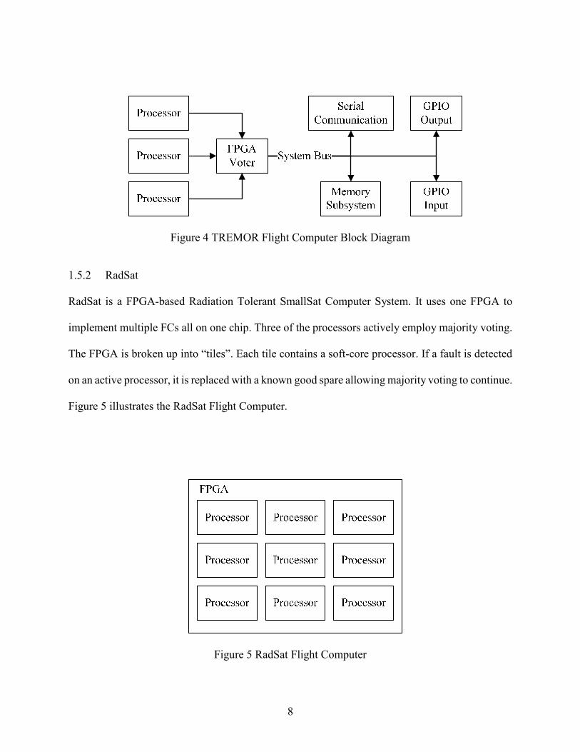
8
Figure 4 TREMOR Flight Computer Block Diagram
1.5.2 RadSat
RadSat is a FPGA-based Radiation Tolerant SmallSat Computer System. It uses one FPGA to
implement multiple FCs all on one chip. Three of the processors actively employ majority voting.
The FPGA is broken up into “tiles”. Each tile contains a soft-core processor. If a fault is detected
on an active processor, it is replaced with a known good spare allowing majority voting to continue.
Figure 5 illustrates the RadSat Flight Computer.
Figure 5 RadSat Flight Computer

9
1.5.3 Dependable Multiprocessor (DM)
The DM system is a cluster of high performance commercial off-the-shelf (COTS) processors
connected with a high speed interconnect. It operates under the control of a reliable, possibly
radiation hardened, system controller. The system controller provides a highly-reliable and SEE-
immune host to support recovery from radiation-induced events in the COTS hardware. A block
diagram of the DM is shown in Figure 6.
System
Controller
COTS
Processor
COTS
Processor………. COTS
Processor
Mass Data
Storage
High Speed Interconnect (Ethernet)
Sensor
I/OSensors
Control Bus (power and discretes)
Spacecraft
Interface
Figure 6 DM Payload Processing Architecture
1.6 Summary
The Quatara system uses full hardware redundancy enclosed in FCRs. It maintains control of the
spacecraft at all times, even when a primary flight computer becomes faulty. A single fault cannot
affect the whole system; it is contained within the FCRs. These properties provide an increase in
reliability for cubeSats which will in turn allow higher risk missions to return valuable science
data. The Quatara system enables low-budget missions to reliably return big budget science.
The TREMOR system restarts all three flight computers after a fault, leaving the spacecraft
unattended for a short time and making it vulnerable to critical failure or losing valuable science

10
data. The Quatara system improves upon this by keeping healthy flight computers on at all times,
even during a fault. TREMOR’s single FPGA voter, although made more robust by TMR, is a
single point of failure. An SEL can affect the entire FPGA IC, faulting the whole system. The
system is only partially redundant. Quatara uses full hardware redundancy so that no one piece of
hardware can fault the entire system. The FPGAs are also enhanced with TMR for additional
robustness.
The RadSat system does not separate the redundant elements with fault containment regions
(FCRs). Fault tolerant systems are built around the concept of FCRs. Its primary goal is to limit
the effects of a fault and the propagation of errors region to region [23]. As a result, an SEL can
affect the entire substrate of the IC, faulting all redundant “healthy” processors. Even if an SEL
does not affect the healthy processors, the fault can only be corrected by cycling power to the entire
FPGA, that is, assuming it has not destructively latched. Like the previous example, this leaves
the spacecraft unattended. The Quatara system improves upon this shortfall by grouping three
complete sets of redundant hardware within three FCRs; one FCR per set. A single fault will only
affect a single set of hardware.
The DM system has excellent throughput but requires a radiation tolerant system controller. This
approach works but suffers increased cost and reduced performance compared to that available
from redundant commercial grade parts. The Quatara system does not require any radiation
tolerant parts, thus providing users with a multitude of economical, high performance commercial
parts. The DM system shares data over a single Ethernet connection which is a single point of
failure. A multi-port Ethernet system could be implemented, but the base unit flight computer

11
would require at least two hardware independent ports. Single board computers ideal for cubeSats
usually only have one port, thereby removing a large portion of design choices. The Quatara
system improves upon this design by providing a dedicated communication bus between each pair
of FPGAs; none are shared. A fault between any two FPGAs will not affect a bus going to the third
FPGA.
1.7 Goals
1) To prove that the proposed architecture is effective against failures caused by SEEs
a. requirements:
i. a working hardware prototype
ii. testing to simulate SEEs
2) To present the architecture and algorithms such that others can improve, build upon, and
scale the system to suit mission parameters.
a. requirements:
i. explicit details about the architecture and hardware used
ii. complete algorithms
iii. flowcharts explaining algorithms
12
Chapter 2 Architecture
As was shown in Figure 1, the architecture consists of three identical strings. A string contains all
of the things needed to command and control the spacecraft if it were operating alone. It is also an
FCR. The major components of a string/FCR in this architecture are a power manager, FPGA
clock source, FPGA, FC, and bus isolator. The major components for string1 are illustrated in
Figure 7.

13
The power management block is used monitor current consumption and remove power from the
string in the event of an overload. This is used to detect SELs and attempt to prevent permanent
damage. It also accepts voting logic from other strings which are logical ANDed together to
remove power. This is the method by which healthy strings majority vote erroneous strings out
and initiate restart. Restarting clears SEEs making strings recoverable.
Figure 7 String Hardware

14
Since the redundancy of the proposed system begins and ends with the flight computer, the IO bus
to the rest of the spacecraft must be shared. A faulty flight computer that is in control of an
instrument has to relinquish control so another can take its place. This is handled with hardware
such that when a faulty FC is voted out, its connection to the bus is automatically broken with a
power reset. This is illustrated as the bus isolator block in Figure 7. When the bus isolator loses
power, its connection to the bus assumes a high impedance. This isolates the FC and completes
the fault containment region.
The FPGA to FPGA data transfer and synchronization signals are illustrated in Figure 8. These
signals are controlled solely by the FPGAs without the FCs’ oversite. This reduces the FCs’
overhead considerably.
Figure 8 FPGA to FPGA Communication
The data transfer sequence is illustrated in Figure 9. It begins with a PPS signal from the FPGA to
the FC signaling that it is time to transfer input data to the FPGA. This is called the primary data
exchange phase. Next is the data interchange phase, where data from each FPGA is exchanged

15
with the other two FPGAs. In the next phase, the combined data return phase, the combined data
is returned to the FC. Each FC now has every other FC’s data including its own. In the final phase,
the decision phase, each FC compares the data and votes out any erroneous string. The primary
FC in command can then control the spacecraft and gather new input data.
Figure 9 Data Transfer
Timing is important for this system to work, yet it is not guaranteed generally by processors. In
microprocessors, interrupts can be triggered for important events but an interrupt, although
seemingly instantaneous, only raises a flag for the processor’s attention. The microprocessor must
perform context switching to service the interrupt if the priority is high enough. This process takes
time and varies depending on what instruction is in action. Similarly, processors with operating
systems would schedule a high priority task, but the time it takes to service that task will vary and
will not be instantaneous. That is why timing is controlled by FPGAs in this system.

16
The data block that is transferred is made up of several parts illustrated in Figure 10. The header
region is unused in this iteration but could be used to pass messages between the FC and FPGA.
The FPGA could for instance pass an error code to the FC indicating that there was no data coming
from one of the other FPGAs. The input region is reserved for instrument data and ground
commands from the FC. The output section contains the FCs’ control solution to the input data.
An example would be the reaction wheel speed needed to adjust the spacecraft’s attitude to point
the solar panels at the sun. Since there is only one round of data exchange, the output solution to
the most recent input data has to be included in the next data exchange cycle. Therefore, cycle N
contains input data N and output data N-1. Cycle times can be adjusted to suit the latency needed.
FCs can also perform the decision phase of the data exchange on every other cycle if desired.
Figure 10 Block Data
Figure 11 indicates how the cycle time, represented by “cycle clocks” later in the algorithm section,
is broken up into windows. The windows here relate directly to the phases illustrated in Figure 11.

17
Initially there is a pulse per second (PPS) signal from the FPGA to the FC indicating that the FC
to FPGA data transfer window is open. The FC can transfer data anytime during that window. The
next window is the FPGA to FPGA data interchange window where the FPGAs exchange the FC’s
data. The final window is the FC final window. A “data ready for FC” flag from the FPGA is sent
to the FC indicating that it can collect the entire set of data.
Figure 11 Data Transfer Windows
18
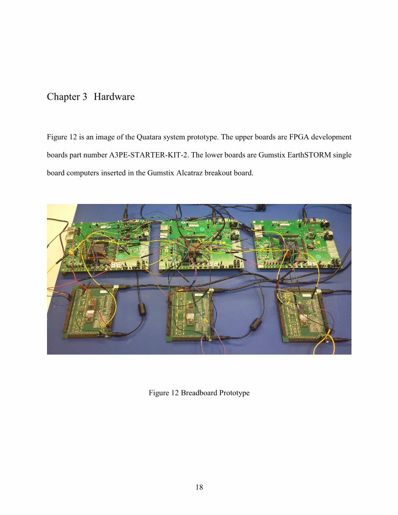
Chapter 3 Hardware
Figure 12 is an image of the Quatara system prototype. The upper boards are FPGA development
boards part number A3PE-STARTER-KIT-2. The lower boards are Gumstix EarthSTORM single
board computers inserted in the Gumstix Alcatraz breakout board.
Figure 12 Breadboard Prototype

19
Figure 13 PCB Prototype
The prototype PCB is shown in Figure 13. While the goal is to achieve PC-104 dimensions (3.55”
X 3.775”), the prototype PCB exceeded that size. Additional hardware was included, e.g.
pushbuttons and headers, to simplify in-depth testing. The next revision can easily meet the size
requirements with the superfluous circuitry removed.
Physical addresses used by the algorithms (discussed later in the algorithm section) are determined
by physical inputs jumpered high or low. Each device has a unique address. The purpose is to
allow a single set of code. Function depends on physical address, not the installed code.
The ProASIC3 flash-based FPGA part number A3P600L-FGG144 was chosen for this
implementation due to its inherent SEU immunity [24], low power draw, and static (flash-based)
configuration property. In fact, this part number uses the same silicon design and process as the
20
fully radiation hardened equivalent RT3PE600L [25]. This gives radiation hardened part
performance at a commercial part price. If a more robust solution is needed the radiation hardened
part can be used since both parts are functionally identical. The low power draw property of flash-
based FPGAs makes them more desirable for this system than static random access memory
(SRAM)-based FPGAs for power limited cubeSats and especially so since the parts are triplicated.
Also, the reduced SEU vulnerability of flash memory also makes this type FPGA more desirable
for space than SRAM for configuration memory [12]. The resources used by the FPGA to
implement the different TMR options for this system are shown in the following tables.
Table 1 shows the resources without TMR enhancement.

21
ProASIC3 Compile Report
Resource: Used: Available: Percent Used:
CORE 4685 38400 12.2%
IO (w/ clocks) 31 147 21.09%
Differential IO 0 65 0%
Global (chip and quadrant) 6 18 33.33%
PLL 0 2 0%
RAM/FIFO 4 60 6.67%
Low Static ICC 0 1 0%
FlashRom 0 1 0%
User JTAG 0 1 0%
Table 1 ProASIC3 Compile Report – No TMR
The C-C option uses combinatorial cells with feedback instead of flip-flop or latch primitives for
storage devices [26]. The resource report using the C-C option is shown in Table 2.
22
ProASIC3 Compile Report
Resource: Used: Available: Percent Used:
CORE 5083 38400 13%
IO (w/ clocks) 31 147 21.09%
Differential IO 0 65 0%
Global (chip and quadrant) 6 18 33.33%
PLL 0 2 0%
RAM/FIFO 4 60 6.67%
Low Static ICC 0 1 0%
FlashRom 0 1 0%
User JTAG 0 1 0%
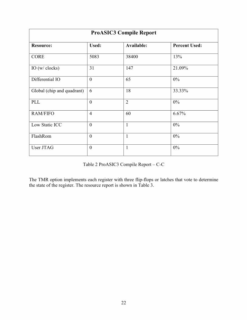
Table 2 ProASIC3 Compile Report – C-C
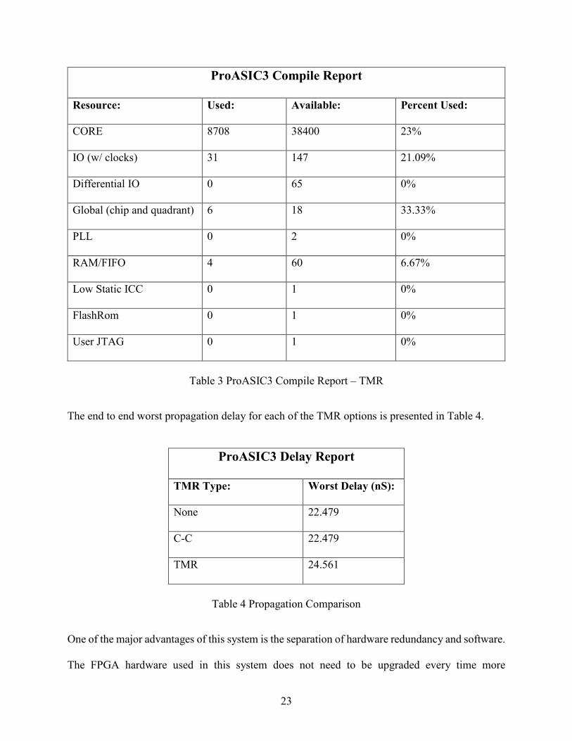
The TMR option implements each register with three flip-flops or latches that vote to determine
the state of the register. The resource report is shown in Table 3.
23
ProASIC3 Compile Report
Resource: Used: Available: Percent Used:
CORE 8708 38400 23%
IO (w/ clocks) 31 147 21.09%
Differential IO 0 65 0%
Global (chip and quadrant) 6 18 33.33%
PLL 0 2 0%
RAM/FIFO 4 60 6.67%
Low Static ICC 0 1 0%
FlashRom 0 1 0%
User JTAG 0 1 0%
Table 3 ProASIC3 Compile Report – TMR
The end to end worst propagation delay for each of the TMR options is presented in Table 4.
ProASIC3 Delay Report
TMR Type: Worst Delay (nS):
None 22.479
C-C 22.479
TMR 24.561
Table 4 Propagation Comparison
One of the major advantages of this system is the separation of hardware redundancy and software.
The FPGA hardware used in this system does not need to be upgraded every time more

24
performance is needed. Keeping everything but the processor will save extensive resources on a
redesign. The same benefit applies if the processor becomes obsolete.

25
Chapter 4 Algorithms
The algorithms presented revolve around the designations “primary”, “secondary”, and “tertiary”.
“Primary” has the most authority with the others descending respectively. While the designations
indicate a hierarchical command structure, it is important to note that they are only states that
determine behavior; they are not assigned specifically to specific hardware. By default, FPGA1 is
“primary”, FPGA2 is “secondary”, and FPGA3 is “tertiary,” but any FPGA can be any designation.
This property is important to prevent a system-wide failure if there is a fault with FPGA1 on a cold
start. A cold start is when all FPGAs are powered up for the first time.
A block diagram, Figure 14, is used to describe the functional relationships of the FPGA code.
The diagram includes the descriptions “FPGA1”, “FPGA2”, and “FPGA3” to simplify
explanation, but the code in all three FPGAs is identical.

26
Figure 14 FPGA Code Block Diagram
The RAM block is the memory storage element for the system. FC block data is stored here. Data
exchange is accomplished by serial peripheral interface (SPI). The window control block controls
the windows in which valid data exchange occurs. Data exchanged outside of valid windows is
considered erroneous and is ignored. The synchronization block is the heart of Quatara providing
timing control for the whole system. Figure 15 pushes into the synchronization control block,
providing more detail of its inner workings.

27
Figure 15 FPGA Code Block Diagram for Synchronization Control
The pulse detector receives the synchronization signals from the other FPGAs, providing the sync
block with the times and types of signals found. The sync block will adjust the cycle time if needed
to make sure the PPS signals are aligned. The proportional-integral-derivative (PID) block
provides closed loop control of the PPS signal adjustment. The universal asynchronous receiver-
transmitter (UART) block transmits the synchronization byte in the form of serial data. This single
unique byte identifies the transmitter’s identity, i.e., the synchronization behavior assumed. This
type of signaling is more complex than discrete strobes but is more robust. Noise transients could
cause false positive synchronization signals. Only valid bytes are accepted.
Figure 16 indicates the major cycle and how the synchronization timing relates. The PPS is sent
between the FPGA and FC. It triggers the FC to start the data exchange function. The green area
in the center of the figure indicates the window in which valid sync pulses can be sent and received.

28
The algorithms are designed to keep the sync pulse in the center of the window. The pulses are
sent from FPGA to FPGA identifying their designation, e.g. primary, secondary, or tertiary.
Figure 16 Synchronization Timing
The pulse detector contains two identical modules, one for each of the other FPGAs. Both operate
in parallel. The flow diagram is presented in Figure 17.

29
Start
Listen for valid sync
pulses (primary,
secondary, tertiary)
from left and right
FPGA and store
Listen for valid sync
pulses from left and
right FPGA and
make sure they
match stored values
Indicate which sync
signals were
detected and the
time they were
detected
Indicate any errors
Clear = 1?
N
Y
Figure 17 Pulse Detector Flow Diagram

30
The pulse detector pseudocode is shown in Figure 18.
//left side
if at any time we get a “reset” signal, zero all registers, state machine back to init state, and
outputs to zero
afterward, if at any time we get a “clear” signal same except stored “left designation” byte and
state machine skips init state and goes to wait4pulse state
otherwise transition through states in state machine starting with “init”
state init:
look at the left uart receiver and see if there’s a new byte
if so, see if equal to “primary” “secondary” or “tertiary”
if so, make sure it isn’t the same as the one detected for the right side, discard otherwise
output “primary detected” “secondary detected” or “tertiary detected”, output the time
detected as “primary time”, “secondary time” or “tertiary time”, and store the received
byte as “left designation”
go to the “wait for pulse” state
state wait for pulse:
look at the left uart receiver and see if there’s a new byte
if so, see if equal to “primary” “secondary” or “terchiary”
if so, make sure it is the same as the one previously stored, discard otherwise
output “primary detected” “secondary detected” or “terchiary detected”, output the time
detected as “primary time”, “secondary time” or “tertiary time”
go to the “wait for clear” state
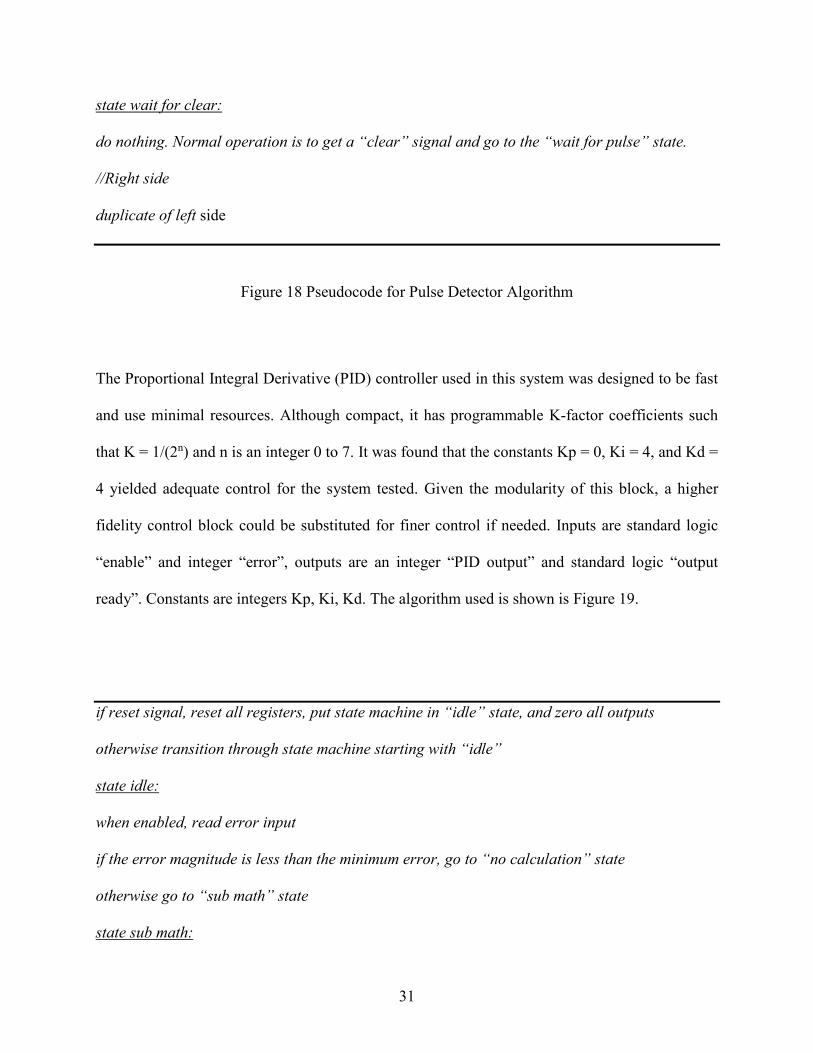
31
state wait for clear:
do nothing. Normal operation is to get a “clear” signal and go to the “wait for pulse” state.
//Right side
duplicate of left side
Figure 18 Pseudocode for Pulse Detector Algorithm
The Proportional Integral Derivative (PID) controller used in this system was designed to be fast
and use minimal resources. Although compact, it has programmable K-factor coefficients such
that K = 1/(2n) and n is an integer 0 to 7. It was found that the constants Kp = 0, Ki = 4, and Kd =
4 yielded adequate control for the system tested. Given the modularity of this block, a higher
fidelity control block could be substituted for finer control if needed. Inputs are standard logic
“enable” and integer “error”, outputs are an integer “PID output” and standard logic “output
ready”. Constants are integers Kp, Ki, Kd. The algorithm used is shown is Figure 19.
if reset signal, reset all registers, put state machine in “idle” state, and zero all outputs
otherwise transition through state machine starting with “idle”
state idle:
when enabled, read error input
if the error magnitude is less than the minimum error, go to “no calculation” state
otherwise go to “sub math” state
state sub math:

32
integral = integral + error //should be integral = integral + error*dt but dt is one here for
//simplicity
derivative = error - prevError //should be derivative = (error - previous_error)/dt but dt is one
//here also
store error as previous error
go to shift state
state shift: // the K-factors used here negative powers of two, i.e. K = 3 means 1/(2^3) = 1/8.
//This simplifies the hardware down to a shift register eliminating the need for a dedicated
//multiplication block and the extra time to perform the multiplication
left shift the error Kp times
left shift the integral Ki times
left shift the derivative Kd times
go to “end sum” state
state end sum:
PID output = error + integral + derivative
state no calculation: don't do calculation; only do min upkeep
PID output = 0
store error as previous error
go to “idle” state
Figure 19 Pseudocode for PID Algorithm

33
The proposed system is asynchronous but is synchronous at the cycle level. Synchronous systems
synchronize at the clock level [23]. The sync algorithm flow diagram and sync pseudocode are
broken up into four separate sections to simplify presentation but exists as one block of code. The
initial synchronization algorithm (part 1 of 4) is shown in Figure 20. It begins with a delay and
assumes one of three behaviors: primary, secondary, or tertiary. For full redundancy capability,
any FPGA can become the primary, secondary, or tertiary, but the normal starting order and the
order used to explain the algorithms is FPGA1 = primary, FPGA2 = secondary, and FPGA3 =
tertiary.
A “park” state transition occurs as a result of certain error checks. In this state it does nothing but
wait. If it’s doing nothing, it isn’t transferring data and the entire string will eventually be voted
out because of a data mismatch. This technique is used to prevent errors from propagating
throughout the system.

34
Start
Physical
address?
1
Wait 1.5 cycles
2
Wait 2.5 cycles
3
Wait 3.5 cycles
Sync signals
Detected?
Primary = 0
Secondary = 0
Tertiary = 0
Primary = 1
Secondary = 0
Tertiary = 0
Primary = 1
Secondary = 1
Tertiary = 0
State “primary
count” of primary
behavior
State “secondary
sync” of secondary
behavior
State “tertiary
sync” of tertiary
behavior
Cold Start Scenarios
State “primary
sync secondary” of
primary behavior
Primary = 0
Secondary = 1
Tertiary = 1
State “secondary
sync” of secondary
behavior
Primary = 1
Secondary = 0
Tertiary = 1Restart Scenarios
State “primary
sync tertiary” of
primary behavior
State “primary
sync secondary” of
primary behavior
Unlikely ScenariosPrimary = 0
Secondary = 0
Tertiary = 1
Primary = 0
Secondary = 1
Tertiary = 0
else
Park
Error Scenario
Figure 20 Sync Flow Diagram

35
The pseudocode for the initial sync block function (part 1 of 4) is shown is Figure 21. Inputs are
integer “cycle clocks”, “start window”, and “decision point”, standard logic “primary detected”,
“secondary detected”, and “tertiary detected”, outputs are byte “primary”, “secondary”, and
“tertiary” and standard logic “pulse per second” and “clear”.
if reset signal, reset all registers, put state machine in “wait4timer” state, and zero all outputs,
“cycle clocks local” = “cycle clocks”
otherwise transition through state machine starting with “wait4timer”
state wait4timer: – wait for timer to complete programmed by physical jumper. FPGA1 timer is
//1.5sec, FPGA2 is 2.5sec, FPGA3 is 3.5sec
when timer done go to “init” state
state init:
//cold start scenarios, i.e. all FPGAs are starting up for the first time
if primary not detected and secondary not detected and tertiary not detected go to “primary
count” state //nothing detected. assert primary fpga
else if primary detected and secondary not detected and tertiary not detected, go to “secondary
sync” state //primary detected. assert secondary fpga
else if primary detected and secondary detected and tertiary not detected, go to “tertiary sync”
state //have primary and secondary. assert tertiary fpga
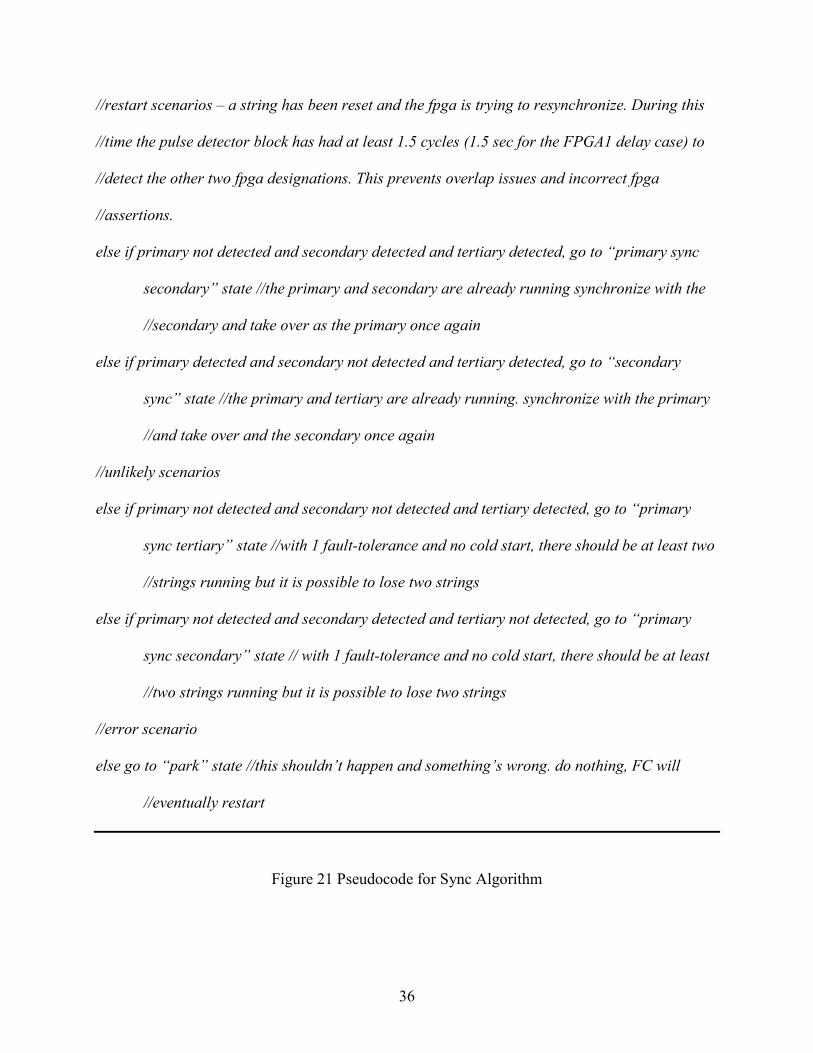
36
//restart scenarios – a string has been reset and the fpga is trying to resynchronize. During this
//time the pulse detector block has had at least 1.5 cycles (1.5 sec for the FPGA1 delay case) to
//detect the other two fpga designations. This prevents overlap issues and incorrect fpga
//assertions.
else if primary not detected and secondary detected and tertiary detected, go to “primary sync
secondary” state //the primary and secondary are already running synchronize with the
//secondary and take over as the primary once again
else if primary detected and secondary not detected and tertiary detected, go to “secondary
sync” state //the primary and tertiary are already running. synchronize with the primary
//and take over and the secondary once again
//unlikely scenarios
else if primary not detected and secondary not detected and tertiary detected, go to “primary
sync tertiary” state //with 1 fault-tolerance and no cold start, there should be at least two
//strings running but it is possible to lose two strings
else if primary not detected and secondary detected and tertiary not detected, go to “primary
sync secondary” state // with 1 fault-tolerance and no cold start, there should be at least
//two strings running but it is possible to lose two strings
//error scenario
else go to “park” state //this shouldn’t happen and something’s wrong. do nothing, FC will
//eventually restart
Figure 21 Pseudocode for Sync Algorithm

37
The primary behavior flow diagram is shown in Figure 22 (part 2 of 4). Although this behavior
has the most authority, it has the simplest function.

38
Figure 22 Primary Behavior Flow Diagram

39
The pseudocode for the primary behavior is shown is Figure 23.
______________________________________________________________________________
//state primary count: Easiest scenario. A free running clock controls outputs; it does not have to
//see what the secondary and tertiary fpgas are doing
counter counts up until it equals “cycle clocks” and resets
if counter = half its max setting output byte “primary”
state primary sync secondary: Here the primary has been reset, the secondary FPGA has taken
//over and the primary is trying to resynchronize with the secondary FPGA before taking back
//over
set counter to half of “cycle clocks”
send “clear” strobe to pulse detector
if secondary detected, go to state “primary count”
state primary sync tertiary: Here the primary has been reset, the tertiary FPGA has taken over
//and the primary is trying to resynchronize with the tertiary FPGA before taking back over
set counter to half its of “cycle clocks”
send “clear” strobe to pulse detector
if tertiary detected, go to state “primary count”
Figure 23 Pseudocode for Primary Behavior Sync Algorithm
40
Figure 24 shows the flow diagram for the secondary behavior (part 3 of 4). Its code is more
complex due to the fact that it has to adjust its own cycle clocks to stay synchronized to the primary
FPGA.

41
Figure 24 Secondary Behavior Flow Diagram

42
Figure 25 shows the pseudocode for the secondary behavior.
state secondary count:
counter counts up and resets when it equals “cycle clocks local”
if counter = zero send out “pulse per second” strobe
if counter is between “start window” and “decision point”, release “clear” output signal
otherwise send “clear” output signal
if counter = half of “cycle clocks local” output byte “secondary”
if counter = “decision point”, go to “secondary decision” state
state secondary decision: we’re at the decision point for the secondary fpga behavior
//this is the ideal scenario where everything is working //fine. The error between the primary and
//secondary fpga sync pulse times are calculated
counter continues counting as before
if “primary detected” and “secondary not detected” then //something wrong if secondary
//detected
PID error = cycle clocks local / 2 – primary time //sync signal should be half of “cycle
//clock local”
go to state “secondary decision 2”
//next is the situation where the primary string has gone off line and we have to take over as
leader

43
else if “primary not detected” and “secondary not detected” and “tertiary detected”, go to
“secondary count” state //check for tertiary to eliminate possibility of lost
//synchronization with other fpgas
else go to “park” state //something is wrong. do nothing until FC resets string
state secondary decision 2:
counter continues counting
if abs(PID error) < max allowed error send to PID block and enable
else go to “park state” //something is wrong. do nothing until FC resets string
when PID block is complete, cycle clocks local = cycle clocks – PID output
go to “secondary count” state
state secondary sync: here the secondary has been reset and needs to synchronize to the primary
//fpga
set counter to half of “cycle clocks local”
send “clear” strobe to pulse detector
if “primary detected”, go to state “primary count”
Figure 25 Pseudocode for Secondary Behavior Sync Algorithm
Figure 26 shows the flow diagram for the tertiary behavior of the sync algorithm (part 4 of 4). Its
operation is nearly identical to the secondary behavior. The difference lies in what happens when
the primary FPGA is lost.

44
Figure 26 Tertiary Behavior Flow Diagram

45
The pseudocode for the tertiary behavior of the sync algorithm is shown in Figure 27.
State tertiary count:
counter counts up and resets when it equals “cycle clocks local”
if counter = zero send out “pulse per second” strobe
if counter is between “start window” and “decision point”, release “clear” output signal
otherwise send “clear” output signal
if counter = half of “cycle clocks local” output byte “tertiary”
if counter = “decision point”, go to “tertiary decision” state
state tertiary decision: we’re at the decision point for the tertiary fpga behavior
//This is the ideal scenario where everything is working fine. The error between the primary and
//tertiary fpga sync pulse times are calculated
counter continues counting as before.
if “primary detected” and “tertiary not detected” then //something wrong if tertiary detected
PID error = cycle clocks local / 2 – primary time //sync signal should be half of “cycle
//clock local”
go to state “tertiary decision 2”
//next is the situation where the primary string has gone off line and we need to follow secondary
else if “primary not detected” and “secondary detected” and “tertiary not detected” //check for
//tertiary to eliminate possibility of lost synchronization with other fpgas
PID error = cycle clocks local / 2 – secondary time //sync signal should be half of “cycle
//clocks local”

46
go to state “tertiary decision 2”
else go to “park” state //something is wrong. do nothing until FC resets string
state tertiary decision 2:
counter continues counting
if abs(PID error) < max allowed error, send to PID block and enable
else go to “park state” //something is wrong. do nothing until FC resets string
when PID block is complete, cycle clocks local = cycle clocks – PID output
go to “tertiary count” state
state tertiary sync: set the count to half point where all sync pulses are found
send “clear” strobe to pulse detector
if “primary detected”, go to state “tertiary count”
state park: sit here and do nothing, don’t make things worse, wait for FC to reset string
indicate error
Figure 27 Pseudocode for Tertiary Behavior

47
Chapter 5 Testing
The following sections detail the tests performed that not only examine the system’s robustness
against SEEs but to also test the faults that would cause system-wide failures in the other systems
discussed previously. The first two tests establish that synchronization, a key for this system to
work, is functioning. The ladder three are designed to test against SEEs and the faults affecting
previous work.
5.1 PPS Period
The FPGA clocks used are identical, and the system could stay synchronized for a while without
any adjustment needed by the algorithms. This test will measure the PPS periods without any
adjustment by the algorithms. The PPS period measurement is shown in Figure 28.
Figure 28 PPS Period Measurement

48
Test1: Enable FPGA1 only. FPGA1 is “primary”. Measure the max and min period between
FPGA1 PPS signals.
Test2: Enable FPGA2 only. FPGA2 is “primary”. Measure the max and min period between
FPGA2 PPS signals.
Test3: Enable FPGA3 only. FPGA3 is “primary”. Measure the max and min period between
FPGA3 PPS signals.
Results:
Period (mS)
PPS Source min max mean
FPGA1 999.97 1,000.0 1,000.0
FPGA2 999.97 1,000.0 999.98
FPGA3 999.90 999.97 999.97
Table 5 Period Test Data
Conclusion: The FPGA clock, although an identical part operating in identical systems, has jitter
and causes the PPS signals to quickly diverge due to lack of synchronization.
Although the worst divergence is only 30µS, the effect accumulates every cycle
and becomes significant in 167 cycles. This test proves the need for a
synchronization algorithm.

49
5.2 Synchronization Accuracy
The degree to which the system can maintain synchronization affects the adjustability of system
cycle time; i.e., shorter cycles can come from tighter synchronization. The accuracy is measured
by the variance shown in Figure 29.
Figure 29 PPS Synchronization Accuracy
Test1: Measure the maximum variance in PPS signals between FPGA1 and FPGA2 during
normal run. Make FPGA1 “primary”.
Test2: Measure the maximum variance in PPS signals between FPGA3 and FPGA2 during
normal run. Make FPGA3 “primary”.
Test3: Measure the maximum variance in PPS signals between FPGA3 and FPGA1 during
normal run. Make FPGA3 “primary”.

50
Figure 30 Synchronization Accuracy Testing
Results:
primary
FPGA
subordinate
FPGA
variance
(µS)
FPGA1 FPGA2 0.651
FPGA3 FPGA1 0.646
FPGA3 FPGA2 0.636
Table 6 Synchronization Accuracy Test Data
Conclusion: Comparing the data from this test and the PPS period test proves that Quatara is
actively aligning the PPSs and providing synchronization for the redundant
elements. Without the previous test for comparison, it could be argued that the

51
system is staying in synchronization because all the parts are identical and the
variance between clock pulses is minimal.
5.3 Interruption of Normal Start Sequence
Since a fault can occur any time on any string, fault on a cold start must be tested as well. By
default, FPGA1 is primary, FPGA2 is secondary, and FPGA3 is tertiary. Power will be withheld
from a single FPGA during the startup sequence and will be applied after the other two FPGAs
complete startup.
Test1: FPGA1 power withheld
Results: FPGA2 initialized as primary, FPGA3 initialized as secondary, FPGA1 initialized as
tertiary.
Test2: FPGA2 power withheld
Results: FPGA1 initialized as primary, FPGA3 initialized as secondary, FPGA2 initialized as
tertiary.
Test3: FPGA3 power withheld
Results: FPGA1 initialized as primary, FPGA2 initialized as secondary, FPGA3 initialized as
tertiary.

52
Conclusion: Interruption of the normal start sequence on a cold start does not cause system
failure. As designed, any FPGA can assume any behavior.
5.4 Random String Reset
A faulty string (one afflicted by an SEU) will be power reset by healthy strings. An SEL will cause
an immediate reset. Resetting strings randomly will simulate these types of failures. This test is
focused on the FPGA’s ability to resynchronize after a power restart. Upon restart, the maximum
divergence between PPS signals will be measured as shown in Figure 31.
Figure 31 Maximum Divergence on Restart
Test1: Wait until all three FPGAs have assumed their behavior. Make FPGA1 primary. Reset
string2 at a random point in its cycle. Measure maximum divergence on restart.
Test2: Wait until all three FPGAs have assumed their behavior. Make FPGA3 primary. Reset
string1 at a random point in its cycle. Measure maximum divergence on restart.

53
Test3: Wait until all three FPGAs have assumed their behavior. Make FPGA3 primary. Reset
string2 at a random point in its cycle. Measure maximum divergence on restart.
Results: All tests concluded with the faulty string restarting, resynchronizing, and assuming
where it left off. The maximum divergence test data is shown in Table 7.
primary
FPGA
subordinate
FPGA
max divergence
(µS)
FPGA1 FPGA2 4.822
FPGA3 FPGA1 10.217
FPGA3 FPGA2 5.322
Table 7 Maximum Divergence on Reset Test Data
Conclusion: The random string reset test proves that the FPGA synchronization algorithm will
recover and continue normal operation after any SEE resulting in a string reset. It
also proves that the system handles faults that previous work could not.
5.5 Voting Logic
An SEE can cause data corruption or cause a component to stop functioning. Comparing shared
data is key for fault detection. Falsifying data in different parts of the normal data stream necessary
to test the voting logic. A simple counting sequence is computed by each FC and is used to
represent the state vector of the system. The output values are compared. The test setup is shown
in Figure 32. Light-Emitting Diodes (LED)s are used to indicate when an FC casts it’s vote for a

54
faulty string. The PCB prototype logic ANDs these signals together and sends them to the power
controller, but LEDs are used in this test to simplify troubleshooting. The test hardware is shown
in Figure 33.
330Ω D1
FC1 GND
330Ω D2
FC2 GND
330Ω D3
FC2 GND
330Ω D4
FC3 GND
330Ω D5
FC1 GND
330Ω D6
FC3 GND
String3
Power
String1
Power
String2
Power
Figure 32 Voting Logic Test Setup
Figure 33 Voting Logic Test Hardware
55
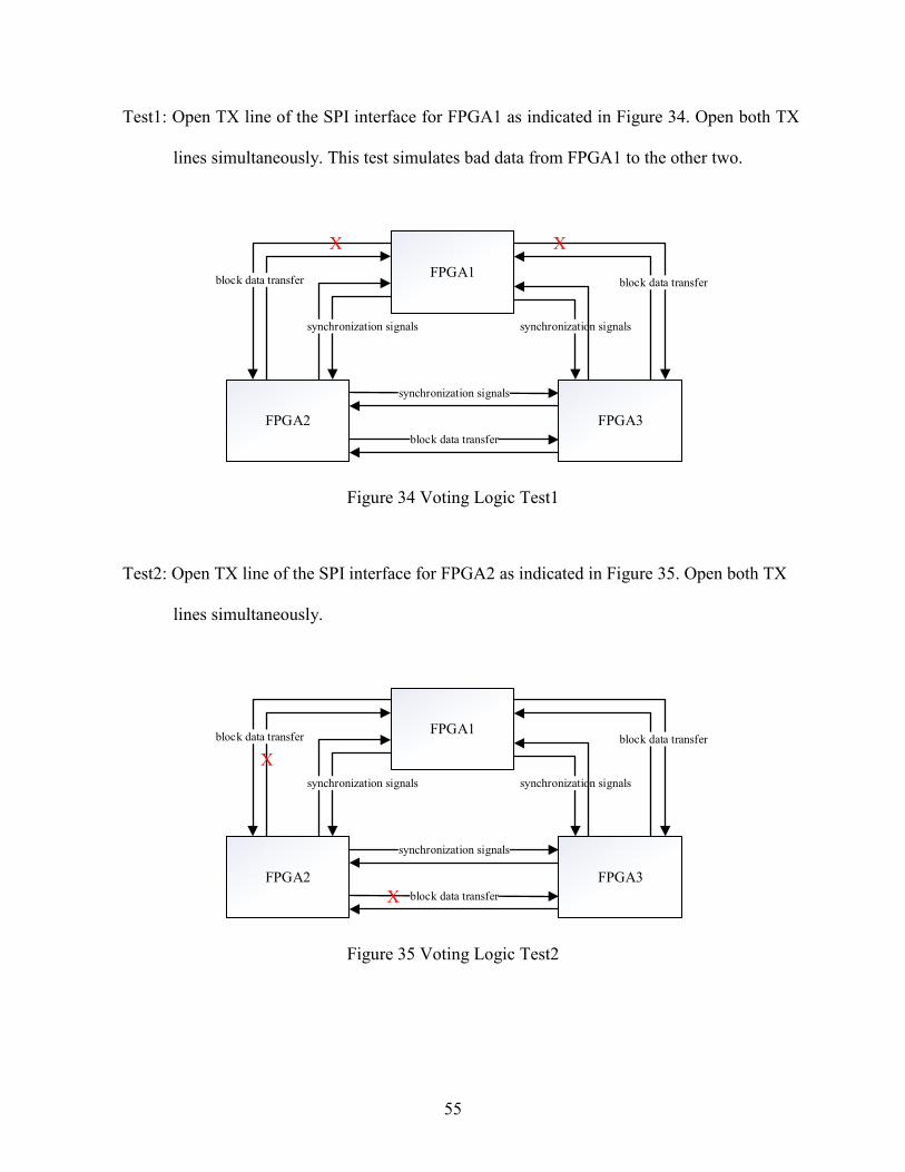
Test1: Open TX line of the SPI interface for FPGA1 as indicated in Figure 34. Open both TX
lines simultaneously. This test simulates bad data from FPGA1 to the other two.
FPGA1
FPGA2 FPGA3
synchronization signals
block data transfer
synchronization signals
block data transfer
synchronization signals
block data transfer
X X
Figure 34 Voting Logic Test1
Test2: Open TX line of the SPI interface for FPGA2 as indicated in Figure 35. Open both TX
lines simultaneously.
FPGA1
FPGA2 FPGA3
synchronization signals
block data transfer
synchronization signals
block data transfer
synchronization signals
block data transfer
X
X
Figure 35 Voting Logic Test2

56
Test3: Open TX line of the SPI interface for FPGA3 as indicated in Figure 36. Open both TX
lines simultaneously.
FPGA1
FPGA2 FPGA3
synchronization signals
block data transfer
synchronization signals
block data transfer
synchronization signals
block data transfer
X
X
Figure 36 Voting Logic Test3
Test4: Open the TX line of the SPI interface for FC1 and FPGA1 as indicated in Figure 37.
This test simulates bad data from FC1 to FPGA1.
FPGA1 FC1
transfer flags
block data transfer
X
Figure 37 Voting Logic Test4
Test5: Open the TX line of the SPI interface for FC2 and FPGA2 as indicated in Figure 38.

57
FPGA2 FC2
transfer flags
block data transfer
X
Figure 38 Voting Logic Test5
Test6: Open the TX line of the SPI interface for FC2 and FPGA2 as indicated in
Figure 39.
FPGA3 FC3
transfer flags
block data transfer
X
Figure 39 Voting Logic Test6
Results: All tests resulted in a pair of LEDs being lit for the faulty string.
Conclusion: Each LED is a vote for a faulty string to be reset. The pair logical ANDed together
produce the reset signal needed by the power management block to perform a power

58
reset on the faulty string. This testing proves that the voting logic detects errors
caused by SEUs in the transferred data block.

59
Chapter 6 Flight Computer
Although beyond the scope of this thesis, some discussion is required regarding the flight computer
software. Although timing and data transfer tasks are handled by the FPGA, the FC still has to
contribute resources to handle voting and deciding who is in charge.
The FCs have a similar order of dominance scheme as the FPGAs, but the designation is
completely independent. Just because the FPGA in a string is “primary” does not mean the FC in
the same string is “primary”. For clarity, the FCs will use a different designation in order of most
authority: General, Captain, and Private.
The voting system is an exact-match voter scheme [23].
The FC basic software flow diagram is shown in Figure 40. The FC hardware selection and FC
software were completed by Jose Molina-Fratichelli [27].

60
Start
PPS signal
detected?
N
Y
send individual
block data
data ready
signal
detected?
N
receive combined
block data
Y
analyze data
and vote
perform other tasks, e.g. built-in self-test,
housekeeping, and/or payload interaction
FC in command
get voted out?
highest authority healthy
FC assumes command
Is there a higher
authority healthy FC?
Am I the FC in
command?
use the shared bus to
gather input data and
command output effectors
N
Y
Y
Y
N
N
Figure 40 FC Software Flow Diagram

61
Requirements levied on computing elements:
1) It is the FC’s responsibility to determine which FC is the General. The General is in
control of the IO bus and thus the spacecraft.
2) If the General is found to be faulty another FC must assume spacecraft control.
3) Every FC must share and collect data when prompted, compare shared data, and vote out
an erroneous FC.
4) FCs must make FPGA triggered synchronization signals the first priority.
5) A FC with a permanent fault must be permanently isolated from the system by the
remaining healthy FCs.

62
Chapter 7 Conclusion
The Quatara flight computer system is a recoverable, redundant, single fault-tolerant system with
increased robustness for cubeSats to serve low-cost, big data missions for NASA, Department of
Defense (DoD), industry, and universities. SEEs and total ionizing dose radiation make cubeSat
FCs perform unreliably. Past work has used redundant hardware to increase reliability. The
Quatara system further improves the robustness of cubeSats by using FCRs containing a full set
of redundant hardware and readily available commercial parts. FPGAs are employed to remove
overhead from the FCs and to accurately control timing. TMR is used to add additional robustness.
The architecture was illustrated from a high level and broken down into smaller parts and
explained. Similarly, the FPGA algorithms were presented as a top-level block diagram with
components explained. The synchronization block, the heart of the system, was broken into sub-
blocks and their functions explained. Synchronization sub-blocks were further presented as both
flow diagrams and pseudocode. The hardware chosen was also discussed.
Testing was designed to examine how the system reacts to major faults caused by the space
environment and to ensure that the algorithms work as predicted. Not only did the Quatara system
pass testing, it validated the improvements to previous work against system-wide failure as well.

63
Chapter 8 Future Work
Future work includes fault-tree development, fault-tree testing, and testing the prototype PCB.
During this research exercise, it was determined that adding the voting logic to the FPGAs would
free up additional overhead for the FCs. Fault-tolerance and redundancy would be completely
separate from software development. FC software developers could then focus on mission specific
tasks, simplifying development. From their perspective, development would be centered around
software development for a sole flight computer; the code would just be installed in all three flight
computers. The FPGAs decide who is in control of the bus and who needs to be reset. Adding the
voting logic to the FPGAs is future work.
One type of fault not tested was a Byzantine fault. This is the most difficult type of fault for three
or more channels with cross channel voting [27]. This fault comes from the Byzantine Generals
Problem [28], an abstract scenario where a group of generals is camped with their troops around
an enemy city. Communicating only via messenger the generals must agree on a common battle
plan. One or more generals may be treacherous though, sending false messages to disrupt reaching
agreement. It takes 3m + 1 generals to cope with m traitors. For the proposed system and single
fault-tolerance, m = 1, it would take four redundant strings to correct this fault whereas this system
only has three. However, if message authentication is used, only m + 2 channels are required [27].
Message authentication is future work.

64
Chapter 9 Bibliography
[1] M. Swartwout, "The First One Hundred CubeSats: A Statistical Look," Journal of
Small Satellites, vol. 2, no. 2, pp. 213-233, 2013.
[2] P. P. Shirvani, "Fault-Tolerant Computing For Radiation Environments," Stanford
University, 2001.
[3] D. Garrison, "email - More Pricing Requests," Envision LLC, 2018.
[4] P. Chambers, "email - Renesas/Intersil Rad Hard Parts Quote," Envision LLC,
2018.
[5] H. Christopher, "email - ProASIC3 Rad Hard Quote," G2 Sales, 2018.
[6] S. Cooke, "email - Price Quote Request," Cobham, 2018.
[7] J. R. J. Sampson, "Dependable Multiprocessor (DM) – High Performance
Computing for CubeSats," Honeywell Aerospace, Clearwater, FL, 2013.
[8] C.-Y. Liu, "A Study Of Flight-Critical Computer System Recovery From Space
Radiation-Induced Error," IEEE, 2001.
[9] R. Angilly, "TREMOR: A Triple Modular Redundant Flight Computer and Fault-
Tolerant Testbed for the WPI PANSAT Nanosatellite," Worchester Polytechnic
Institute.
[10] D. W. Caldwell, "Minimalist Fault-Tolerance Techniques for Mitigating Single-
Event Effects in Non-Radiation Hardened Microcontrollers," University of
California Los Angeles, 1998.
[11] J. M. Johnson, "Synchronization Voter Insertion Algorithms for FPGA Designs
Using Triple Modular Redundancy," Brigham Young University, 2010.

65
[12] L. S. Parobek, "Research, Development and Testing of a Fault-tolerant FPGA-
Based Sequencer for CubeSat Launching Applications," Calhoun: The Naval
Postgraduate School Archive, Monterey, California, 2013.
[13] S. Sayil, "Space Radiation Effects on Technology and Human Biology,"
Beaumont.
[14] A. J. T. W. A. Kristina Rojdev, "Preliminary Radiation Analysis of the Total
Ionizing Dose," NASA Technical Reports Server, 2015.
[15] K. A. L. C. P. Janet L. Barth, "Radiation Assurance for the Space Environment,"
IEEE, pp. 323-333, 2004.
[16] A. B. W. H. S. P J Botma, "Low Cost Fault Tolerant Techniques for Nano/Pico-
Satellite Applications," IEEE, 2013.
[17] S. Monk, Programming FPGAs: Getting Started with Verilog, McGraw-Hill, 2017.
[18] J. Rajewski, Learning FPGAs: Digital Design for Beginners with Mojo and Lucid
HDL, Sebastopol, CA: O'Reilly Media, Inc., 2017.
[19] Y. Haigang, Z. Jia, S. Jiabin and Y. Le, "Review of Advanced FPGA Architectures
and Technologies," Institute of Electronics, Chinese Academy of Sciences, Beijing,
China, 2014.
[20] D. J. Smith, HDL Chip Design, Madison, AL: Doone Publications, 1996.
[21] R. C. J. Singleterry, J. Sobieszczanski-Sobieski and S. Brown, "Field-
Programmable Gate Array Computer In Structural Analysis: An Initial
Exploration," AIAA.
[22] B. F. Dutton, "Embedded Soft-Core Processor-Based Built-In Self-Test of Field
Programmable Gate Arrays," Auburn University, 2010.
[23] R. W. Butler, "A Primer on Architectural Level Fault Tolerance," Langley
Research Center, Hampton, VA, 2007.
[24] M. F. C. P. H. K. K. L. Melanie Berg, "Taming the Single Event Upset (SEU)
Beast - Approaches and Results for Field Programmable Gate Array (FPGA)
Devices and How to Apply Them," NEPP Electronic Technology Workshop, 2011.
[25] Microsemi, "RT ProASIC3," 31 May 2018. [Online]. Available:
https://www.microsemi.com/product-directory/rad-tolerant-fpgas/1696-rt-proasic3.

66
[26] Microsemi, "Using Synplify to Design in Microsemi Radiation-Hardened FPGAs,"
Microsemi, 2012.
[27] J. Molina-Fraticelli, S. Peeples and P. Capo-lugo, "2nd Generation QUATARA
Flight Computer Project," NASA, Huntsville, AL, 2014.
[28] B. A. O'Connell, "Achieving Fault Tolerance via Robust Partitioning and N-
Modular Redundancy," MIT, 2007.
[29] R. S. M. P. Leslie Lamport, "The Byzantine Generals Problem," ACM
Transactions on Programming Languages and Systems, vol. 4, no. 3, pp. 382-401,
1982.
[30] J. R. J. Sampson, "Small, Light-Weight, Low-Power, Low-Cost, High Performance
Computing for CubeSats," Clearwater, FL, 2014.
Top Related