


Languages
Pages
Legal


Chapter 1
Conduction in Semiconductors
1.1 Introduction
All solid-state devices, e.g. diodes and transistors, are fabricated from materials known as semi-conductors. In order to understand the operation of these devices, the basic mechanism of howcurrents flow in them must be understood. This chapter covers the fundamentals of conductionin semiconductors. The chapter is not intended to be an extensive introduction to the area ofsolid-state physics. Instead, only those topics which lead to a better understanding of the macro-scopic properties of semiconductors are covered. The mechanisms of conduction in a metal and ina semiconductor are compared. The effects of impurities on conduction in semiconductors are dis-cussed. The formation of a p-n semiconductor junction is described and its conduction propertiesare discussed.
1.2 Classification of Conductors
Figure 1.1 illustrates a two-dimensional view of an atom that is called the Bohr model of the atom.It consists of a positively charged nucleus and a system of negatively charged electrons which rotatesaround the nucleus. In a neutral atom, the total charge is zero. This means that the positive chargeon the nucleus is equal to the total negative charge on the electrons. The electrons are bound tothe nucleus by the forces of attraction between oppositely charged particles. They are arrangedsystematically in layers called shells. The closer a shell is to the nucleus, the more tightly boundare the electrons in that shell to the atom. The shell closest to the nucleus can contain no morethan two electrons. The outer shell can have no more than eight. The number in the shells inbetween is determined by the laws of quantum mechanics.
The outermost shell in an atom contains what are called the valence electrons. These governthe nature of chemical reactions of the elements. In addition, they play a large part in determiningthe electrical behavior of the elements and the crystalline structure of solids. The metallic elementstend to have one, two, or three valence electrons. The nonmetals have five, six, or seven. The inertgases have eight. The class of elements which have four valence electrons is called semiconductors.If a valence electron escapes its parent atom, it becomes free to move about. The parent atom thenhas a net positive charge and is called an ionized atom or an ion. If an electric field is applied to amaterial, the free electrons have forces exerted on them which cause them to move. This constitutesthe flow of a current in the material that is called a conduction current or a drift current.
1

2 CHAPTER 1. CONDUCTION IN SEMICONDUCTORS
Figure 1.1: Two-dimensional Bohr model of an atom showing the nucleus and three shells.
Depending on the number n of free electrons per unit volume in a solid, the material is classifiedas being a good conductor, a semiconductor, or an insulator. For a good conductor, n is very largeand is independent of temperature. A typical value is n ' 1028 per m3. For an insulator at ordinarytemperatures, n is much smaller and has a typical value n ' 107 per m3. For a semiconductor, itlies between the values for a good conductor and an insulator and is a function of the temperature.Silicon is an important semiconductor for which n ' 1.5 × 10¹⁶ per m3 at room temperature(T = 300K).
1.3 Conduction in Metals
Metals are classified as good conductors. The valence electrons are so loosely bound to the atomsthat they are free to move about in the conductor. Fig. 1.2 shows a two-dimensional illustration ofthe atoms in a metal with the free electrons distributed randomly among the immobile ions. Thefree electrons can be visualized as molecules of a gas that permeate the region between the ions.Analogous to the random motion of molecules in a gas, thermal energy causes the free electronsto be in continuous random motion. Observation of an individual electron would reveal that itsdirection of motion changes randomly after each collision with an ion. Because the direction ofmotion of each electron is random, the average number of electrons passing through any area perunit time is zero. Thus the average current flow in the metal is zero.
1.3.1 Drift Velocity
If an electric field−→E (V/m) is applied to a metal, an electrostatic force is exerted on the free
electrons which causes a conduction current to flow. (The arrow indicates a vector quantity.)The force on an individual electron is given by
−→F = −q−→E (N), where q is the electronic charge
(q = 1.602× 10⁻¹⁹C). The electrostatic forces cause the electrons to be accelerated in a directionopposite to that of the applied field. Fig. 1.3 illustrates the path that an individual electron mighttake under the influence of the electric field. If the electron did not collide with the bound ions, itsvelocity would increase indefinitely. However, energy is lost with each collision so that the average

1.3. CONDUCTION IN METALS 3
Figure 1.2: Two-dimensional view of the atoms in a metal with free electrons distributed randomlyamong the ions.
velocity approaches a constant or steady-state value. The average velocity −→v (m/ s) is called thedrift velocity. It is proportional to the applied field and is given by
−→v = −µe−→E (1.1)
where µe (m2V−1 s−1) is the electron mobility. (The minus sign is required because the negative
charge on the electron causes it to move is a direction opposite to the field.) The average distancethat the electron travels between collisions with the bound ions is called the mean free path. Asthe temperature increases, the bound ions vibrate with increasing intensity, causing the mean freepath between collisions to decrease. This effect causes the drift velocity −→v to decrease, which ismodeled by a decrease in the electron mobility µe with temperature.
Figure 1.3: Path taken by a free electron in a metal under the influence of an applied electric field.
1.3.2 Charge Density
The charge density ρ (C/m3) in a conductor is defined as the free charge per unit volume. Torelate the charge density in a metal to the density of free electrons, let n be the number of electrons
4 CHAPTER 1. CONDUCTION IN SEMICONDUCTORS
per m3. Because the charge per electron is −q, it follows that the free charge per unit volume inthe metal is given by
ρ = −nq (1.2)
1.3.3 Current Density
The current density−→J (A/m2) in a conductor is defined as the current per unit area flowing in a
particular direction. To relate the current density in a conductor to the drift velocity of the movingcharges, consider a section of wire of length ∆ in which a current I is flowing. This is illustratedin Fig. 1.4. The charge in the section is ∆Q = ρ∆V = ρS∆ , where ρ is the charge density and Sis the cross-sectional area of the wire. Let ∆t be the time required for the charge in the section tomove the distance ∆ . The velocity of the charge is −→v = ba∆ /∆t, where ba is a unit vector in thedirection of current flow. The current I flowing in the area S is I = ∆Q/∆t. It follows that thecurrent density
−→J can be related to the drift velocity −→v as follows:
−→J = ba I
S= ba∆Q
S∆t= baρS∆
S∆t= ρ
µba∆∆t
¶= ρ−→v (1.3)
Figure 1.4: Section of wire of length ∆ in which a current I flows.
1.3.4 Conductivity
Using Eqs. (1.1) through (1.3), we can relate the current density−→J to the electric field
−→E in a
metal as follows: −→J = ρ−→v = (−nq)
³−µe−→E´= nqµe
−→E = σ
−→E (1.4)
(Note that two minus signs have canceled so that−→J is in the direction of
−→E .) This equation defines
the conductivity σ (Ω−1m−1) of the metal. It is given by
σ = nqµe (1.5)
Because n is independent of temperature in a metal, it follows that the decrease in electron mobilityµe with temperature causes the conductivity σ to decrease with temperature.

1.4. CONDUCTION IN INTRINSIC SEMICONDUCTORS 5
Example 1 Aluminum has three valence electrons per atom, an atomic weight of 0.02698 kg/mol,a density of 2700 kg/m3, and a conductivity of 3.54 × 10⁷ S/m−1. Calculate the electron mobilityin aluminum. Assume that all three valence electrons in each atom are free.
Solution. Recall from introductory chemistry that a mole of any substance is a quantity equalto its atomic weight and contains a number of molecules equal to Avogadro’s number which is6.02× 1023. It follows that the number of aluminum atoms per m3 is
6.02× 10²³ atomsmol
× 1
0.02698
mol
kg× 2700 kg
m3= 6.024× 1028 atoms
m3
Thus the electron density in the aluminum is n = 3 × 6.024 × 1028 = 1.807 × 1029 per m3. FromEq. (1.5), the mobility is given by
µe =σ
nq=
3.54× 1076.024× 1028 × 1.602× 10−19 = 3.67× 10
−3m2V−1 s−1
1.3.5 Resistance
Consider the section of wire illustrated in Fig. 1.4. A conduction current I is flowing in the wire sothat the current density is
−→J = baI/S, where ba is a unit vector in the direction of current flow and
S is the cross-sectional area. Let V be the voltage drop across the section of length ∆ so that theelectric field in the section is
−→E = baV/∆ . With the aid of Eq. (1.4), we can write
−→J = baσV/∆ .
By equating the two relations for−→J , we obtain
−→J = ba I
S= baσV∆
(1.6)
This equation can be solved for the resistance R of the section of wire to obtain
R =V
I=∆
σS(1.7)
Thus the resistance is directly proportional to the length of the wire and inversely proportional toits area. Because the conductivity σ decreases with temperature, it follows from this equation thatR increases with temperature. In most metals, the resistance increases linearly with temperature.
Example 2 The conductivity of copper is 5.8 × 10⁷ S/m. If a 1m length of copper wire has aresistance of 1Ω, what is the thickness of the wire? Assume a circular cross section.
Solution. Let d be the diameter of the wire. Using Eq. (1.7), we can write S = π (d/2)2 =∆ /σR = 1/
¡5.8× 107 × 1¢. Solution for d yields d = 0.148mm.
1.4 Conduction in Intrinsic Semiconductors
Semiconductors are the class of elements which have four valence electrons. Two important semi-conductors are germanium (Ge) and silicon (Si). Early solid-state electronic devices were fabricatedalmost exclusively from germanium, whereas modern devices are fabricated almost exclusively fromsilicon. Gallium arsenide (GaAs) is a semiconductor compound made up of gallium, which has three

6 CHAPTER 1. CONDUCTION IN SEMICONDUCTORS
valence electrons, and arsenic, which has five. This semiconductor is making inroads in digital ap-plications which require extremely high switching speeds and in extremely high-frequency analogapplications. However, silicon remains the most useful semiconductor material and is expected todominate for many years to come.
Semiconductor materials are normally in crystalline form with each valence electron shared bytwo atoms. The semiconductor is said to be intrinsic if it is not contaminated with impurity atoms.Fig. 1.5 shows a two-dimensional view of an intrinsic semiconductor crystal. Each circle representsboth the nucleus of an atom and all electrons in that atom except the valence electrons. The linksbetween the circles represent the valence electrons. Each valence electron can be assumed to spendhalf time with each of two atoms so that each atom sees eight half-time electrons. Compared to ametal, the valence electrons in a semiconductor are tightly bound.
Figure 1.5: Two-dimensional illustration of the crystal lattice of an intrinsic semiconductor.
The thermal energy stored in a semiconductor crystal lattice causes the atoms to be in constantmechanical vibration. At room temperature, the vibrations shake loose several valence electronswhich then become free electrons. In intrinsic silicon, the number of free electrons is approximatelyone in 1012 of the total number of valence electrons. The free electrons behave similarly to thosein a metal. Under the influence of an applied electric field, they have a mobility and exhibit adrift velocity which produces a conduction current. However, because of the small number of freeelectrons, the conductivity of an intrinsic semiconductor is much lower than that of a metal.
When an electron is shaken loose from an atom, an electron vacancy is left which is called ahole. The parent atom then becomes an ion. The constant mechanical vibration of the latticecan cause the ion to capture a valence electron from a neighboring atom to replace the missingone. When such a transfer takes place, the position of the hole moves from one atom to another.This is equivalent to a positive charge +q moving about in the semiconductor. (The motion of ahole can be likened to the motion of a bubble in water.) Like free electrons, holes have a mobilityand exhibit a drift velocity which produces a conduction current under the influence of an appliedelectric field. Because of the opposite charge polarity of electrons and holes, they drift in oppositedirections under the influence of a field.
Figure 1.6 illustrates the drift of free electrons in an intrinsic semiconductor under the applica-tion of an electric field that is directed from left to right. When an electron is shaken loose from itsvalence shell, an electron-hole pair is formed. The force generated by the electric field causes the

1.4. CONDUCTION IN INTRINSIC SEMICONDUCTORS 7
free electrons to drift to the left. Fig. 1.7 illustrates the drift of holes. In effect, a hole drifts to theright when a bound valence electron shifts to the left from one atom to another. The arrows in thefigure point from the new position of a hole to its former position, i.e. in the direction of movementof the bound electrons in the lattice. The movement of holes may be likened to the movement ofbubbles of air in water, where the water represents the bound electrons and the bubbles representthe holes. The movement of a bubble in one direction is really the result of a movement of waterin the opposite direction. In summary, the flow of current in the semiconductor is the result ofthe flow of two components. One component is the flow of free electrons in one direction. Theother component is the flow of the absence of bound electrons in the other direction. Because ofthe opposite charge polarities, the electron current and the hole current add to produce the totalconduction current.
Figure 1.6: Illustration of the drift of free electrons under the application of an external electricfield.
1.4.1 Recombinations
Because hole-electron pairs are continually created by thermal agitation of a semiconductor lattice,it might seem that the number of holes and free electrons would continually increase with time. Thisdoes not happen because free electrons are continually recombining with holes. At any temperature,a stable state is reached when the creation rate of hole-electron pairs is equal to the recombinationrate. The mean lifetime τn ( s) of a free electron is the average time that the electron exists in thefree state before recombination. The mean lifetime τp ( s) for the hole is defined similarly. In theintrinsic semiconductor, τn is equal to τp because the number of free electrons must be equal tothe number of holes. However, the addition of an impurity to the semiconductor lattice can causethe mean lifetimes to be unequal.
1.4.2 Intrinsic Concentration
Denote the number of free electrons per m3 in a semiconductor by n and the number of holes per m3
by p. In an intrinsic semiconductor, the hole concentration must equal the electron concentration.

8 CHAPTER 1. CONDUCTION IN SEMICONDUCTORS
Figure 1.7: Illustration of the drift of holes under the application of an external electric field.
In this case we write n = p = ni, where ni is called the intrinsic concentration. It can be shownthat ni can be written
ni = n0T3/2 exp
µ−VG2VT
¶(1.8)
where n0 is a constant, T is the absolute temperature, VG is the semiconductor bandgap voltage,and VT is the thermal voltage. (The bandgap voltage multiplied by q represents the minimumenergy required to cause a bound valence electron to become a free electron.) For silicon, thebandgap voltage at T = 300K has the value VG = 1.11V. The thermal voltage is related to thetemperature by
VT =kT
q(1.9)
where k is the Boltzmann constant (k = 1.381 × 10⁻²³ J/K). At T = 300K, the thermal voltagehas the value VT = 0.0259V.
Example 3 The initial temperature of a specimen of silicon is T1 = 300K. By what factor doesthe intrinsic concentration ni increase if the temperature increases by 10 C (18 F)? Assume thebandgap voltage at both temperatures is VG = 1.11V.
Solution. Let T1 = 300K be the initial temperature and T2 = 310K the final temperature. At300K, the thermal voltage is VT1 = 0.0259V. At 310K, it is VT2 = (1.380× 10−23 × 310)/1.602×10−19 = 0.0267V. The factor by which ni increases is calculated from Eq. (1.8) as follows:
ni2ni1
=(T2)
3/2 exp (−VG/2VT2)(T1)
3/2 exp (−VG/2VT1)=
µ310
300
¶3/2exp
·1.11
2
µ −10.0267
+1
0.0259
¶¸= 2.0
1.4.3 Conductivity
When an electric field−→E is applied to an intrinsic semiconductor, the free electrons drift with a ve-
locity −→v e = −µe−→E , where µe is the electron mobility. The holes drift with a velocity
−→v h = +µh−→E ,

1.5. N-TYPE AND P-TYPE SEMICONDUCTORS 9
where µh is the hole mobility. Although the free electrons and holes drift in opposite directions,the current densities add because the charge polarities are opposite. The electron charge density isρe = −niq and the hole charge density is ρh = +niq , where ni is the intrinsic concentration. Thetotal conduction current density can be written
−→J = ρe
−→v e + ρh−→v h = ni (µe + µh) q
−→E = σ
−→E (1.10)
This equation defines the conductivity σ of the intrinsic semiconductor. It is given by
σ = ni (µe + µh) q (1.11)
Example 4 A rod of intrinsic silicon is 1 cm long and has a diameter of 1mm. At room temper-ature, the intrinsic concentration in the silicon is ni = 1.5 × 10¹⁶ per m3. The electron and holemobilities are µe = 0.13m
2V−1 s−1 and µh = 0.05m2V−1 s−1. Calculate the conductivity σ of the
silicon and the resistance R of the rod.
Solution. The conductivity is calculated from Eq. (1.11) as follows:
σ = ni (µe + µh) q = 1.5× 1016 × (0.13 + 0.05)× 1.602× 10−19= 4.33× 10⁻⁴ S/m
The resistance is calculated from Eq. (1.5) as follows:
R =∆
σS=
0.01
4.33× 10⁻⁴ × π (0.5× 10⁻³)2 = 29.4MΩ
1.5 n-Type and p-Type Semiconductors
The preceding example illustrates how poor a conductor intrinsic silicon is at room temperature.The conductivity can be increased by adding certain impurities in carefully controlled minutequantities. When this is done, the semiconductor is called a doped semiconductor. There are twoclasses of impurities that are used. These are donor impurities and acceptor impurities. Typicallyone impurity atom is added per 108 semiconductor atoms. A semiconductor that is doped with adonor impurity is called an n-type semiconductor. One that is doped with an acceptor impurity iscalled a p-type semiconductor.
1.5.1 n-Type Semiconductor
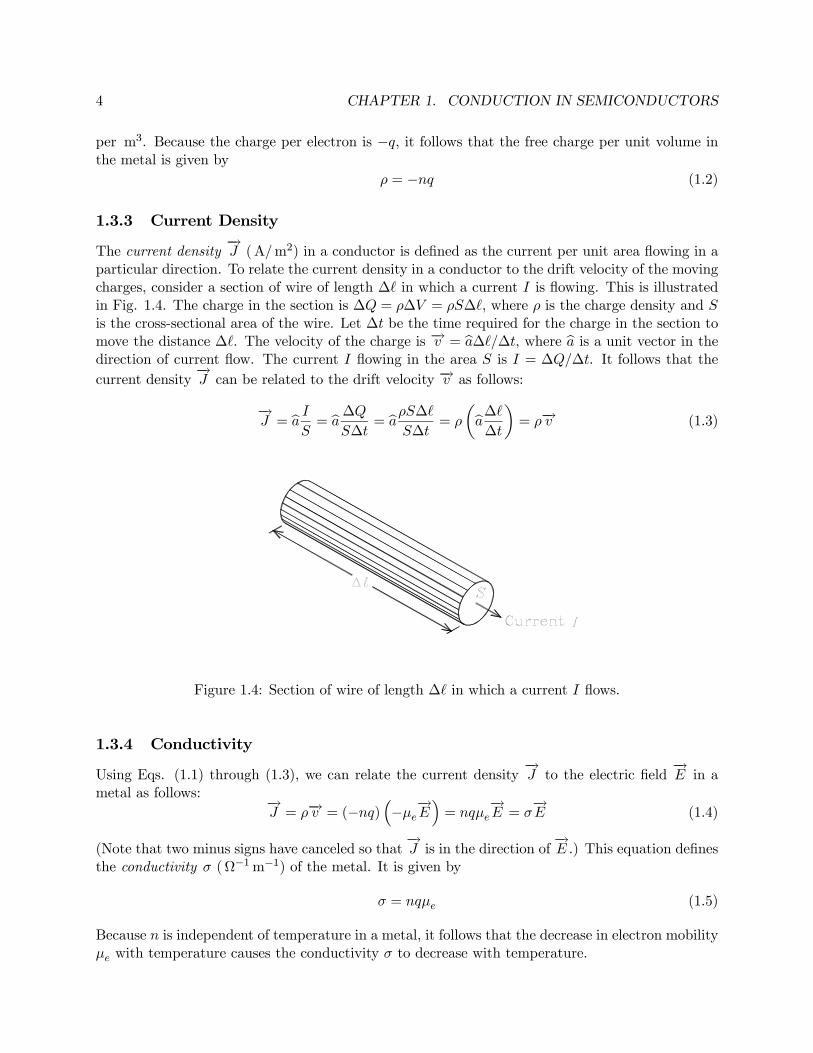
An n-type semiconductor is produced by adding a donor impurity such as arsenic, antimony, orphosphorus to an intrinsic semiconductor. Each donor atom has five valence electrons. When adonor atom replaces an atom in the crystal lattice, only four valence electrons are shared withthe surrounding atoms. The fifth valence electron becomes a free electron as illustrated in Fig.1.8. The number of free electrons donated by the donor atoms is much greater than the numberof free electrons and holes in the intrinsic semiconductor. This makes the conductivity of the n-type semiconductor much greater that of the intrinsic semiconductor. Because the number of freeelectrons is far greater than the number of holes, the free electrons are the majority carriers. Thesemiconductor is called n-type because the majority carriers have a negative charge.
10 CHAPTER 1. CONDUCTION IN SEMICONDUCTORS
Figure 1.8: Two-dimensional illustration of the crystal lattice of an n-type semiconductor
Hole-electron pairs are continually formed by thermal agitation of the lattice in an n-typesemiconductor. Because of the large number of donor electrons, there are many more free electronsavailable for recombination with the holes. This decreases the mean lifetime for the holes whichdecreases the number of holes in the n-type semiconductor compared to the intrinsic semiconductor.For this reason, the current due to the flow of holes in an n-type semiconductor is often neglectedin calculations.
It is important to understand that a donor atom is electrically neutral if its fifth valence electrondoes not become a free electron in the lattice. If the fifth electron becomes a free electron, thenumber of protons in the atom is greater than the number of electrons by one. In this case, thedonor atom becomes a bound positively charged ion.
1.5.2 p-Type Semiconductor
A p-type semiconductor is produced by adding an acceptor impurity such as gallium, boron, orindium to an intrinsic semiconductor. Each acceptor atom has three valence electrons. When anacceptor atom replaces an atom in the crystal lattice, there are only three valence electrons sharedwith the surrounding atoms. This leaves a hole as illustrated in Fig. 1.9. The number of holescreated by the acceptor atoms is much greater than the number of free electrons and holes in theintrinsic semiconductor. This makes the conductivity of the p-type semiconductor much greaterthat of the intrinsic semiconductor. Because the number of holes is far greater than the numberof electrons, the holes are the majority carriers. The semiconductor is called p-type because themajority carriers have a positive charge.
Hole-electron pairs are continually formed by thermal agitation of the lattice in a p-type semicon-ductor. Because of the large number of holes, there are many more holes available for recombinationwith the free electrons. This decreases the mean lifetime for the free electrons which decreases thenumber of electrons in the p-type semiconductor compared to the intrinsic semiconductor. For thisreason, the current due to the flow of free electrons in a p-type semiconductor is often neglected incalculations.
It is important to understand that an acceptor atom is electrically neutral if the hole created bythe absence of its fourth valence electron is not filled by an electron from an adjacent silicon atom.

1.5. N-TYPE AND P-TYPE SEMICONDUCTORS 11
Figure 1.9: Two-dimensional illustration of the crystal lattice of a p-type semiconductor.
Once an electron fills the hole, the number of electrons in that atom is greater than the number ofprotons by one. In this case, the acceptor atom becomes a bound negatively charged ion.
1.5.3 Mass-Action Law
In an intrinsic semiconductor, we have noted that the electron concentration and the hole concen-tration are both equal to the intrinsic concentration, i.e. n = p = ni. If this were not true, thematerial would not be electrically neutral. We have seen that adding an n-type impurity to thesemiconductor increases n and decreases p. Similarly, adding a p-type impurity increases p anddecreases n. It can be shown that the product of n times p is a constant independent of the dopingtype and the doping level. The product is given by
np = n2i (1.12)
where ni is given by Eq. (1.8). This relation is called the mass-action law.To understand this equation, consider an intrinsic semiconductor in which n = p = ni. Assume
that donors with the density DA = ni are added to the semiconductor at t = 0. This initiallydoubles the total number of free electrons, which causes the recombination rate with the holes todouble. This causes the hole density to drop from ni to ni/2. The initial free electron densityis 2ni which drops to 2ni − ni/2 after the increase in recombinations. Thus the product of theelectron and hole concentrations is (2ni − ni/2) × ni/2 = 3n2i /4. Now suppose that the numberof donors is increased by the factor N , where N is large. In this case, the product becomes(Nni − ni/N)×ni/N = n2i
¡1− 1/N2
¢ ' n2i . Although this is not an exact proof, it illustrates thebasic mechanism. A more detailed proof requires an involved thermodynamic analysis.
1.5.4 Electrical Neutrality
An intrinsic semiconductor is electrically neutral, i.e. there is no net charge stored. The additionof n-type or p-type impurities does not change this. To state this mathematically, let ND be thenumber of donor atoms per m3 and NA the number of acceptor atoms per m3. We assume that alldonor atoms and all acceptor atoms are ionized so that there are ND bound positive charges per
12 CHAPTER 1. CONDUCTION IN SEMICONDUCTORS
m3 and NA bound negative charges per m3. Each donor ion has a charge +q and each acceptorion has a charge −q. The total number of negative charges per m3 is equal to the number n of freeelectrons per m3 plus the number NA of bound acceptor atoms per m3, i.e. n+NA. Similarly, thenumber of positive charges per m3 is equal to the number p of holes per m3 plus the number ND
of bound donor atoms per m3, i.e. p+ND. Because the semiconductor is electrically neutral, thenumber of positive charges must equal the number of negative charges. This gives the condition
n+NA = p+ND (1.13)
In an n-type semiconductor, NA = 0 and p << n so that the above equation can be solved forn to obtain
n = p+ND ' ND (1.14)
The approximation in this equation and Eq. (1.12) can be used to solve for the hole concentrationp to obtain
p ' n2iND
(1.15)
Similarly, in a p-type semiconductor, we can write
p = n+NA ' NA (1.16)
n ' n2iNA
(1.17)
Example 5 In the silicon rod of Example 4, the number of silicon atoms per m3 is 5 × 1028. Adonor impurity is added to the silicon in the concentration of one donor atom per 108 atoms ofsilicon. Calculate the new resistance of the rod. Assume that each donor atom contributes one freeelectron.
Solution. The donor concentration in the silicon is calculated as follows:
ND = 5× 1028 atomsm3
× 1
1× 10⁸donorsatom
= 5× 10²⁰donorsm3
It follows from Eq. (1.14) that the free electron concentration is n ' ND = 5× 10²⁰ electronsper m3. From Eq. (1.15), the hole concentration is p ' n2i /n = (1.5× 10¹⁵)2/5× 1020 = 4.5× 10⁹holes per m3. Because p << n, we can neglect p in calculating the conductivity. Eq. (1.11) givesσ ' nqµe = 5 × 1020 × 1.602 × 10−19 × 0.13 = 10.41 S/m. The resistance is calculated from Eq.(1.5) as follows:
R =∆
σS=
0.01
10.41× π (0.5× 10⁻³)2 = 1.22 kΩ
Compared to the intrinsic silicon rod of Example 2, this is smaller by a factor of 24, 100.It is possible to add both an acceptor impurity and a donor impurity to an intrinsic semiconduc-
tor. If the donor concentration ND is equal to the acceptor concentration NA, the semiconductorremains intrinsic because the free electrons of the donors combine with the holes of the acceptors.With ND = NA, Eqs. (1.12) and (1.13) give n = p = ni. If ND > NA, the semiconductor becomesan n-type. In this case, Eqs. (1.14) and (1.15) become
n = p+ND −NA ' ND −NA (1.18)

1.5. N-TYPE AND P-TYPE SEMICONDUCTORS 13
p ' n2iND −NA
(1.19)
Similarly if NA > ND, the semiconductor becomes a p-type and Eqs. (1.16) and (1.17) hold if NA
is replaced by NA −ND.p = n+NA −ND ' NA −ND (1.20)
n ' n2iNA −ND
(1.21)
1.5.5 Conductivity
The conduction current density in an intrinsic semiconductor is given by Eq. (1.10). In a dopedsemiconductor, it is given by −→
J = (nµe + pµh) q−→E = σ
−→E (1.22)
where n is the electron concentration and p is the hole concentration. This equation defines theconductivity σ. It is given by
σ = (nµe + pµh) q (1.23)
For an intrinsic semiconductor, n = p = ni and this equation reduces to Eq. (1.11).
1.5.6 Diffusion Current
In an n-type or a p-type semiconductor, it is possible to have a component of current that is not aconduction current. This current is due to the non-uniform density of free electrons or holes andis called a diffusion current. It is not possible to have a diffusion current in a metal. To achievea non-uniform density of free electrons or holes, the doping concentration in the semiconductoris not constant, i.e. it is a function of position. Such a concentration is called a graded dopingconcentration.
Figure 1.10 illustrates a semiconductor in which the concentration of holes is a function of thecoordinate z, i.e. p = p (z). In addition, p (z) is a decreasing function of z. Consider the planedefined by z = z1. Because the number of holes to the left of the plane is greater than the numberto the right, it is reasonable to expect that the random motion of the holes due to thermal energywould cause more holes to migrate from left to right than from right to left. Thus there is a netcurrent flow across the plane from left to right. This current is called a diffusion current.
In general, the hole diffusion current density is given by
−→J p = −qDh∇p (1.24)
where Dh is the hole diffusion constant and ∇p is the gradient or directional derivative of p. If bx,by, and bz, respectively, are unit vectors in the x, y, and z directions, ∇p is given by
∇p = bx∂p∂x+ by ∂p
∂y+ bz ∂p
∂z(1.25)
For the case illustrated in Fig. 1.10, p is a function of z only so that ∇p = bzdp/dz. (The totalderivative is used because p is a function of z only.) Because p (z) is a decreasing function of z inthe figure, it follows that dp/dz < 0. This makes the direction of the diffusion current in the +zdirection.
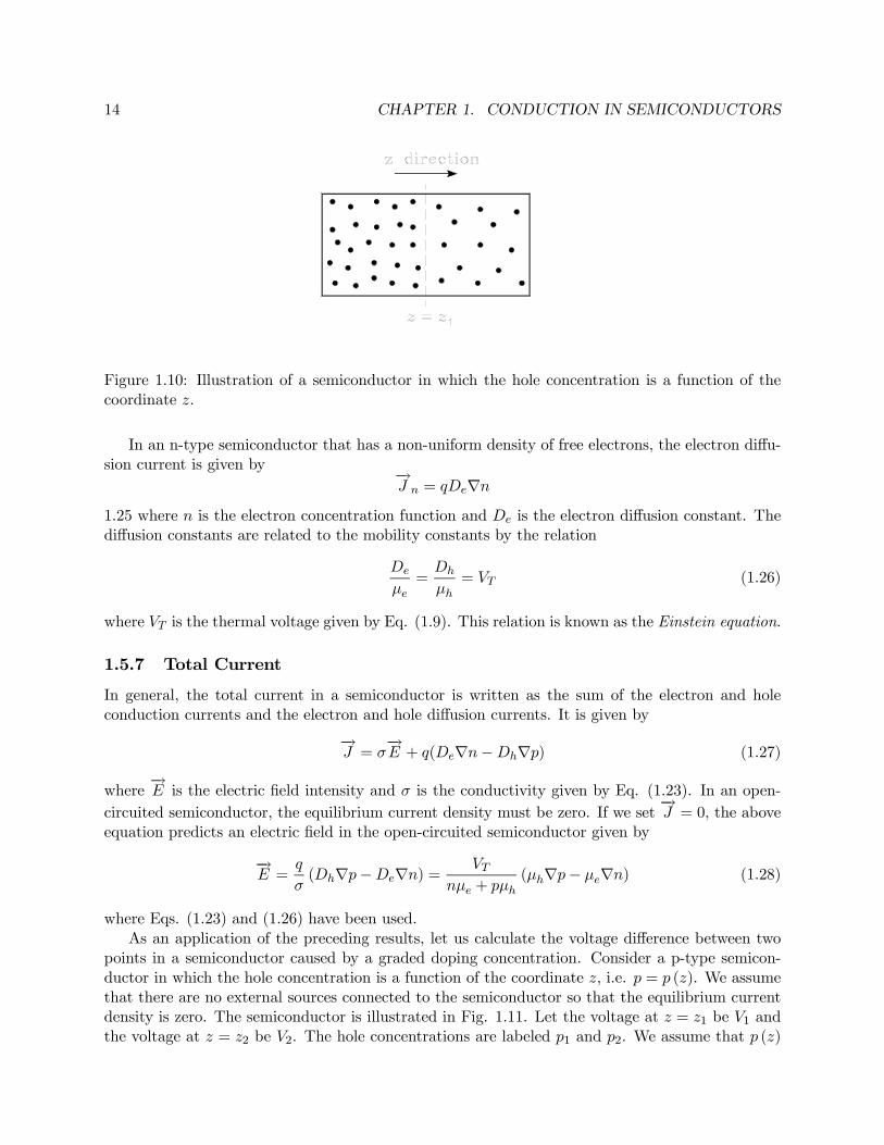
14 CHAPTER 1. CONDUCTION IN SEMICONDUCTORS
Figure 1.10: Illustration of a semiconductor in which the hole concentration is a function of thecoordinate z.
In an n-type semiconductor that has a non-uniform density of free electrons, the electron diffu-sion current is given by −→
J n = qDe∇n1.25 where n is the electron concentration function and De is the electron diffusion constant. Thediffusion constants are related to the mobility constants by the relation
De
µe=
Dh
µh= VT (1.26)
where VT is the thermal voltage given by Eq. (1.9). This relation is known as the Einstein equation.
1.5.7 Total Current
In general, the total current in a semiconductor is written as the sum of the electron and holeconduction currents and the electron and hole diffusion currents. It is given by
−→J = σ
−→E + q(De∇n−Dh∇p) (1.27)
where−→E is the electric field intensity and σ is the conductivity given by Eq. (1.23). In an open-
circuited semiconductor, the equilibrium current density must be zero. If we set−→J = 0, the above
equation predicts an electric field in the open-circuited semiconductor given by
−→E =
q
σ(Dh∇p−De∇n) = VT
nµe + pµh(µh∇p− µe∇n) (1.28)
where Eqs. (1.23) and (1.26) have been used.As an application of the preceding results, let us calculate the voltage difference between two
points in a semiconductor caused by a graded doping concentration. Consider a p-type semicon-ductor in which the hole concentration is a function of the coordinate z, i.e. p = p (z). We assumethat there are no external sources connected to the semiconductor so that the equilibrium currentdensity is zero. The semiconductor is illustrated in Fig. 1.11. Let the voltage at z = z1 be V1 andthe voltage at z = z2 be V2. The hole concentrations are labeled p1 and p2. We assume that p (z)

1.5. N-TYPE AND P-TYPE SEMICONDUCTORS 15
is a decreasing function of z so that p1 > p2. This gives an electric field−→E that is directed in the
negative z direction.Because there are more holes at z1 than at z2, it may seem that the electric field should be
directed from left to right. To understand why it is directed to the left, assume that p1 = p2initially. In this case, there is no initial electric field. At t = 0, let the hole density at z1 beincreased by the addition of acceptors. As t increases, some of the holes at z1 diffuse toward z2,leaving bound negative ions at z1. The diffusion of holes toward z2 increases the net positive chargeat z2. Thus the voltage at V2 becomes positive with respect to the voltage at V1 and the electricfield is directed from right to left. When equilibrium is reached, the net current flow is zero becausethe force generated by the electric field cancels the diffusion force.
Figure 1.11: p-type semiconductor with nonuniform doping.
To solve for the electric field−→E , we set n = 0 and ∇p = bazdp/dz in Eq. (1.28) to obtain
−→E = baz VT
p
dp
dz(1.29)
Because−→E is related to the voltage or potential function V by
−→E = −∇V and V = V (z), it follows
that−→E = −bzdV/dz. By equating the two expressions for −→E , we obtain
bzVTp
dp
dz= −bz dV
dz(1.30)
when the bz and the dz are canceled from both sides of the equation, we obtain
dV = VTdp
p
This can be integrated to obtain
V2 − V1 = VT ln
µp1p2
¶(1.31)
It follows that the voltage difference depends only on the concentrations at the two points andis independent of the separation of the points. A similar equation can be derived for the voltagedifference as a function of the free electron concentration n in an n-type semiconductor. It is givenby
V2 − V1 = −VT lnµn1n2
¶(1.32)

16 CHAPTER 1. CONDUCTION IN SEMICONDUCTORS
1.6 The Open-Circuited p-n Junction
A p-n junction is the junction between an n-type semiconductor and a p-type semiconductor. Itis fabricated by introducing donor impurities into one side of an intrinsic semiconductor crystaland acceptor impurities into the other side. The transition between the two regions occurs in avery small distance, typically 0.5µm. Fig. 1.12 illustrates the cross section of a p-n junction wherethe donor ions are represented by positive signs and the acceptor ions are represented by negativesigns. Initially, we assume that the only charge carriers in the n-type side are free electrons andthat the only charge carriers in the p-type side are holes.
Figure 1.12: Diagram of a p-n junction with the width of the depletion region greatly exaggerated.
Because of the unequal electron concentrations and unequal hole concentrations on the twosides of the junction, a diffusion current consisting of both holes and free electrons will flow acrossthe junction. (The diffusion process is similar to the diffusion of different gases between two glassjars joined at the mouths.) Holes diffuse out of the p-type side and into the n-type side and freeelectrons diffuse out of the n-type side and into the p-type side. This causes the p-type side tobecome negatively charged and the n-type side to become positively charged. The charges causean electric field to build up across the junction which is directed from the n-type side to the p-typeside. The polarity of the electric field is such that the force it exerts on the holes and free electronsopposes the diffusion process. Equilibrium is reached when the force exerted on the charge carriersby the electric field is equal to the diffusion force.
Let us now consider what happens when thermal agitation of the semiconductor lattice producesa hole-electron pair in the region near the junction. The electric field directed from the n-type sideto the p-type side exerts a force on the free electron and causes it to be swept to the n-type side.Similarly, the hole is swept to the p-type side. The directions that the charges move are opposite tothose due to the diffusion process. When equilibrium is reached, the net number of both electronsand holes crossing the junction is zero.
1.6.1 Depletion Region
Because no free electrons or holes can exist is the region about the junction, there are no mobilecharges to neutralize the ions in this region. This is illustrated in Fig. 1.12. The ions on the

1.6. THE OPEN-CIRCUITED P-N JUNCTION 17
n-type side have a positive charge on them and those on the p-type side have a negative charge.These charges are called uncovered charges. The region about the junction in which the uncoveredcharges exist is called the depletion region. Other names for this are the space-charge region andthe transition region. Fig. 1.13a illustrates the plot of the net uncovered charge density in thep-n junction as a function of distance from the junction. The charge distribution is called a dipoledistribution because the charge on one side of the junction is the negative of the charge on theother side. The uncovered charges on each side of the junction can be thought of as the charges onthe plates of a parallel plate capacitor as shown in Fig. 1.13b.
Figure 1.13: (a) Plot of the charge density as a function of distance from the junction. (b) Parallelplate capacitor analog of the charge distribution.
Because of charge neutrality, the total uncovered charge on the n-type side of the depletionregion must be equal to the negative of the total uncovered charge on the p-type side. If then and p concentrations are equal, it follows that the widths of the uncovered charge regions onthe two sides of the junction must be equal. Now, suppose the p concentration is increased whileholding the n concentration constant. Charge neutrality requires the width of the p-type side ofthe depletion region to decrease if the total uncovered charge is to remain constant. Similarly, ifthe n concentration is increased while holding the p concentration constant, the width of the n-typeside must decrease. We conclude, in general, that increasing either p or n or both decreases thetotal width w of the depletion region illustrated in Fig. 1.13a. This has an important effect on thereverse-bias breakdown characteristics of a junction. This is discussed in the following chapter.
1.6.2 Built-In Potential
Because there is an electric field in the depletion region of a p-n junction that is directed from then-type side to the p-type side, it follows that there is a difference in potential or voltage across thejunction. This voltage difference is called the built-in potential or the contact potential. It can becalculated from either Eq. (1.31) or Eq. (1.32). Let us use Eq. (1.32). In this equation, p1 is thehole concentration in the p-type side and p2 is the hole concentration in the n-type side. By Eq.(1.16) the hole concentration in the p-type side is p1 ' NA, where NA is the acceptor concentrationper m3. By Eq. (1.15) the hole concentration in the n-type side is p2 ' n2i /ND, where ni is theintrinsic concentration per m3 and ND is the donor concentration per m3. It follows from Eq.
18 CHAPTER 1. CONDUCTION IN SEMICONDUCTORS
(1.32) that the built-in potential VB is is given by
VB = VT ln
µNAND
n2i
¶(1.33)
The same result is obtained from Eq. (1.31).
Example 6 An open-circuited p-n junction is fabricated from silicon. The acceptor and donorconcentrations are NA = ND = 5× 10²⁰ per m3. The intrinsic concentration is ni = 1.5× 10¹⁶ perm3. Solve for the built-in potential at room temperature.
Solution. The thermal voltage at room temperature is VT = 0.0259V. By Eq. (1.33), thebuilt-in potential has the value
VB = VT ln
µNAND
n2i
¶= 0.0259 ln
" ¡5× 10²⁰¢2
(1.5× 10¹⁶)2#= 0.539V
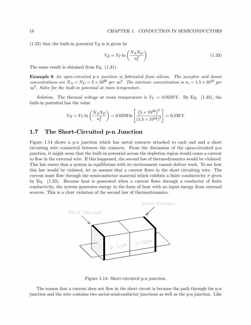
1.7 The Short-Circuited p-n Junction
Figure 1.14 shows a p-n junction which has metal contacts attached to each end and a shortcircuiting wire connected between the contacts. From the discussion of the open-circuited p-njunction, it might seem that the built-in potential across the depletion region would cause a currentto flow in the external wire. If this happened, the second law of thermodynamics would be violated.This law states that a system in equilibrium with its environment cannot deliver work. To see howthis law would be violated, let us assume that a current flows in the short circuiting wire. Thecurrent must flow through the semiconductor material which exhibits a finite conductivity σ givenby Eq. (1.23). Because heat is generated when a current flows through a conductor of finiteconductivity, the system generates energy in the form of heat with no input energy from externalsources. This is a clear violation of the second law of thermodynamics.
Figure 1.14: Short-circuited p-n junction.
The reason that a current does not flow in the short circuit is because the path through the p-njunction and the wire contains two metal-semiconductor junctions as well as the p-n junction. Like

1.8. THE BIASED P-N JUNCTION 19
the p-n junction, both metal-semiconductor junctions exhibit a built-in potential. The algebraicsum of the three built-in potentials is zero so that there is no net voltage to cause a current to flowin the wire and the second law of thermodynamics is not violated.
The characteristics of metal-semiconductor junctions differ primarily from those of p-n junctionsin two ways. First, they conduct current well in both directions. Second, the built-in potentialdoes not change when a current flows through the junction. Junctions which have these propertiesare called ohmic junctions or nonrectifying junctions. We will see in the following that the p-njunction does not have the properties of an ohmic junction. (Not all metal-semiconductor junctionsare ohmic. The Schottky-barrier diode is an example which is described in the following chapter.)
1.8 The Biased p-n Junction
1.8.1 Reverse Bias
Figure 1.15 shows a p-n junction with a dc source connected to it. The polarity of the source ischosen so that the positive terminal is connected to the n-type side and the negative terminal isconnected to the p-type side. The current that flows across the junction consists of two components,a diffusion current caused by unequal carrier concentrations on the two sides of the junction and aconduction current caused by the electric field across the junction. With VS = 0, these two currentsexactly cancel each other so that the net current is zero.
Figure 1.15: Reverse biased p-n junction.
Now let us examine what happens when VS > 0. Because negative charge is attracted by apositive voltage and positive charge is attracted by a negative voltage, both the free electrons inthe n-type side and the holes in the p-type side are pulled away from the junction. This causesthe width of the depletion region to increase so that there are more uncovered charges on each sideof the junction. This is illustrated in Fig. 1.15 compared to Fig. 1.12. The potential across thejunction which opposes diffusion is increased by the applied bias to the value VB + VS, where VB

20 CHAPTER 1. CONDUCTION IN SEMICONDUCTORS
is the built-in potential. This is greater than VB so that the electric field across the junction isincreased. Because the diffusion force on the charge carriers is opposed by the force exerted by thiselectric field, it follows that the diffusion current is decreased by the applied voltage. The diffusioncurrent approaches zero as VS is increased.
Although the diffusion current goes to zero, the conduction current due to thermally producedhole-electron pairs in the depletion region continues to flow across the junction. When such ahole-electron pair is generated, the electric field across the junction causes the electron to be sweptto the n-type side and the hole to be swept to the p-type side. This causes a very small current toflow in the external circuit in the direction indicated in Fig. 1.15. Because the current is so small,the junction is said to be reverse biased.
1.8.2 Forward Bias
Figure 1.16 shows the p-n junction with the polarity of the dc source chosen so that the positiveterminal is connected to the p-type side and the negative terminal is connected to the n-typeside. Because positive charge is repelled by a positive voltage and negative charge is repelled bya negative voltage, both the free electrons in the n-type side and the holes in the p-type side areforced toward the junction. This causes the width of the depletion region to decrease so that thereare fewer uncovered charges on each side of the junction. This is illustrated in Fig. 1.16 comparedto Fig. 1.12. The potential across the junction which opposes diffusion is decreased by the appliedbias to the value VB − VS , where VB is the built-in potential. This is less than VB so that theelectric field across the junction is decreased. This decreases the force which opposes diffusion sothat the diffusion current increases rapidly as VS is increased. Because a large current flows, thejunction is said to be forward biased.
Figure 1.16: Forward biased p-n junction.
It might seem that the potential across the junction which opposes diffusion could be madeto go to zero by increasing VS. Should this happen, the width of the depletion region would go

1.8. THE BIASED P-N JUNCTION 21
to zero and the current would become arbitrarily large. This cannot happen in a physical p-njunction because the resistance of the semiconductor material and the resistances of the externalmetal contacts limit the current. If we denote the sum of the resistances by R, the net potentialacross the junction which opposes diffusion is VB− (VS − IR) = VB−VS+ IR. This relation showsthat the voltage drop across R counteracts the effect of VS on the voltage which opposes diffusionand this in turn limits the current.
Top Related