


Languages
Pages
Legal


1010101010101010101010101010101010101010101010101010101010101010101010101010101010
1010101010101010101010101010101010101010101010101010101010101010101010101010101010
1010101010101010101010101010101010101010101010101010101010101010101010101010101010
1010101010101010101010101010101010101010101010101010101010101010101010101010101010
1010101010101010101010101010101010101010101010101010101010101010101010101010101010
1010101010101010101010101010101010101010101010101010101010101010101010101010101010
1010101010101010101010101010101010101010101010101010101010101010101010101010101010
1010101010101010101010101010101010101010101010101010101010101010101010101010101010
1010101010101010101010101010101010101010101010101010101010101010101010101010101010
1010101010101010101010101010101010101010101010101010101010101010101010101010101010
1010101010101010101010101010101010101010101010101010101010101010101010101010101010
1010101010101010101010101010101010101010101010101010101010101010101010101010101010
1010101010101010101010101010101010101010101010101010101010101010101010101010101010
1010101010101010101010101010101010101010101010101010101010101010101010101010101010
10101010101010101010101010101010101010101010101010101010101010101010101010101010
1010101010101010101010101010101010101010101010101010101010101010101010101010101010
1010101010101010101010101010101010101010101010101010101010101010101010101010101010
101010101010101010101010101010101010101010101010101010101010101001010101010101010
1010101010101010101010101010101010101010101010101010101010101010101010101010101010
1010101010101010101010101010101010101010101010101010101010101010101010101010101010
1010101010101010101010101010101010101010101010101010101010101010101010101010101010
1010101010101010101010101010101010101010101010101010101010101010101010101010101010
1010101010101010101010101010101010101010101010101010101010101010101010101010101010
Contents:
Binary Parallel Adder.
BCD Adder.
Magnitude Comparator.
Decoders.
Encoders.
Multiplexer
Demultiplexer.
ROM
PLA
Combinational Logic with MSI and LSI
Prepared By
Mohammed Abdul kader
Assistant Professor, EEE, IIUC
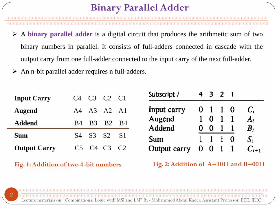
A binary parallel adder is a digital circuit that produces the arithmetic sum of two
binary numbers in parallel. It consists of full-adders connected in cascade with the
output carry from one full-adder connected to the input carry of the next full-adder.
An n-bit parallel adder requires n full-adders.
Lecture materials on "Combinational Logic with MSI and LSI" By- Mohammed Abdul Kader, Assistant Professor, EEE, IIUC 2
Binary Parallel Adder 101010101010101010101010101010101010101010101010101010101010101010101010101010101010101010101010101010101010101010101010101
010101010101010101010101010101010101010101010101010101010101010101010101010101010101010101010101010101010101010101010101010
010101010101010101010101010101010101010101010101010101010101010101010101010101010101010101010101010101010101010101010
010101010101010101010101010101010101010101010101010101010101010101010101010101010101010101010101010101010101010101010
Input Carry C4 C3 C2 C1
Augend A4 A3 A2 A1
Addend B4 B3 B2 B4
Sum S4 S3 S2 S1
Output Carry C5 C4 C3 C2
Fig. 1: Addition of two 4-bit numbers Fig. 2: Addition of A=1011 and B=0011

Lecture materials on "Combinational Logic with MSI and LSI" By- Mohammed Abdul Kader, Assistant Professor, EEE, IIUC 3
Binary Parallel Adder (Cont.) 101010101010101010101010101010101010101010101010101010101010101010101010101010101010101010101010101010101010101010101010101
010101010101010101010101010101010101010101010101010101010101010101010101010101010101010101010101010101010101010101010101010
010101010101010101010101010101010101010101010101010101010101010101010101010101010101010101010101010101010101010101010
010101010101010101010101010101010101010101010101010101010101010101010101010101010101010101010101010101010101010101010
Figure-3, shows the interconnection of four full-adder (FA) circuits to provide a 4-bit
binary parallel adder. The augend bits of A and the addend bits of B are designated by
subscript numbers from right to left. The input carry to adder is C1 and the output carry is
C5.
Fig. 3: 4-bit full adders
Lecture materials on "Combinational Logic with MSI and LSI" By- Mohammed Abdul Kader, Assistant Professor, EEE, IIUC 4
Binary Parallel Adder (Cont.) 101010101010101010101010101010101010101010101010101010101010101010101010101010101010101010101010101010101010101010101010101
010101010101010101010101010101010101010101010101010101010101010101010101010101010101010101010101010101010101010101010101010
010101010101010101010101010101010101010101010101010101010101010101010101010101010101010101010101010101010101010101010
010101010101010101010101010101010101010101010101010101010101010101010101010101010101010101010101010101010101010101010
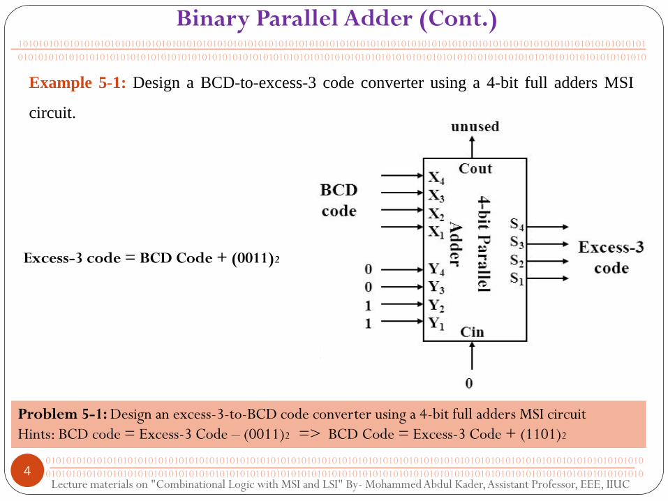
Example 5-1: Design a BCD-to-excess-3 code converter using a 4-bit full adders MSI
circuit.
Excess-3 code = BCD Code + (0011)2
Problem 5-1: Design an excess-3-to-BCD code converter using a 4-bit full adders MSI circuit
Hints: BCD code = Excess-3 Code – (0011)2 => BCD Code = Excess-3 Code + (1101)2
Lecture materials on "Combinational Logic with MSI and LSI" By- Mohammed Abdul Kader, Assistant Professor, EEE, IIUC 5
101010101010101010101010101010101010101010101010101010101010101010101010101010101010101010101010101010101010101010101010101
010101010101010101010101010101010101010101010101010101010101010101010101010101010101010101010101010101010101010101010101010
010101010101010101010101010101010101010101010101010101010101010101010101010101010101010101010101010101010101010101010
010101010101010101010101010101010101010101010101010101010101010101010101010101010101010101010101010101010101010101010
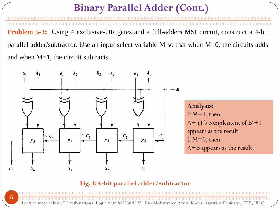
Problem 5-3: Using 4 exclusive-OR gates and a full-adders MSI circuit, construct a 4-bit
parallel adder/subtractor. Use an input select variable M so that when M=0, the circuits adds
and when M=1, the circuit subtracts.
Fig. 4: 4-bit parallel adder/subtractor
Analysis:
If M=1, then
A+ (1’s complement of B)+1
appears as the result
If M=0, then
A+B appears as the result.
Binary Parallel Adder (Cont.)
Lecture materials on "Combinational Logic with MSI and LSI" By- Mohammed Abdul Kader, Assistant Professor, EEE, IIUC 6
101010101010101010101010101010101010101010101010101010101010101010101010101010101010101010101010101010101010101010101010101
010101010101010101010101010101010101010101010101010101010101010101010101010101010101010101010101010101010101010101010101010
010101010101010101010101010101010101010101010101010101010101010101010101010101010101010101010101010101010101010101010
010101010101010101010101010101010101010101010101010101010101010101010101010101010101010101010101010101010101010101010
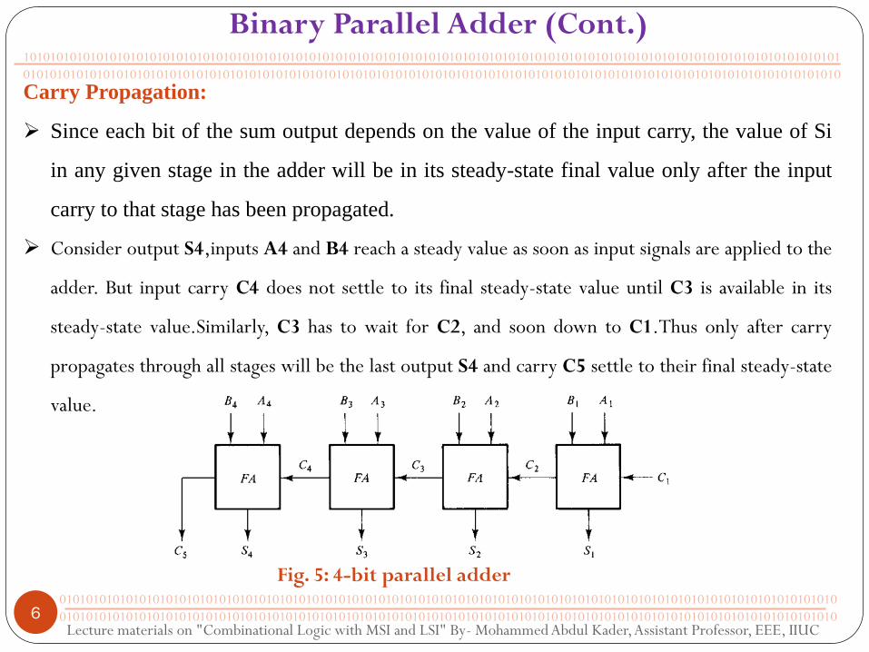
Carry Propagation:
Since each bit of the sum output depends on the value of the input carry, the value of Si
in any given stage in the adder will be in its steady-state final value only after the input
carry to that stage has been propagated.
Consider output S4,inputs A4 and B4 reach a steady value as soon as input signals are applied to the
adder. But input carry C4 does not settle to its final steady-state value until C3 is available in its
steady-state value.Similarly, C3 has to wait for C2, and soon down to C1.Thus only after carry
propagates through all stages will be the last output S4 and carry C5 settle to their final steady-state
value.
Binary Parallel Adder (Cont.)
Fig. 5: 4-bit parallel adder

Lecture materials on "Combinational Logic with MSI and LSI" By- Mohammed Abdul Kader, Assistant Professor, EEE, IIUC 7
101010101010101010101010101010101010101010101010101010101010101010101010101010101010101010101010101010101010101010101010101
010101010101010101010101010101010101010101010101010101010101010101010101010101010101010101010101010101010101010101010101010
010101010101010101010101010101010101010101010101010101010101010101010101010101010101010101010101010101010101010101010
010101010101010101010101010101010101010101010101010101010101010101010101010101010101010101010101010101010101010101010
Carry Propagation (Cont….):
The number of gate levels for the carry propagation can be found from the circuit of the
full-adder.
The signals at Pi and Gi settle to their steady-state value after the propagation through the
irrespective gates. These two signals are common to all FAs and depend only on the input augend
and addend bits.
The signals from the input carry 𝐶𝑖, to the output carry 𝐶𝑖+1 propagates through an AND
and an OR gate, which constitute two gate levels.
For an n-bit parallel adder, there are 2n gate levels for the carry to propagate through.
Binary Parallel Adder (Cont.)
Fig. 6: Full adder

Lecture materials on "Combinational Logic with MSI and LSI" By- Mohammed Abdul Kader, Assistant Professor, EEE, IIUC 8
101010101010101010101010101010101010101010101010101010101010101010101010101010101010101010101010101010101010101010101010101
010101010101010101010101010101010101010101010101010101010101010101010101010101010101010101010101010101010101010101010101010
010101010101010101010101010101010101010101010101010101010101010101010101010101010101010101010101010101010101010101010
010101010101010101010101010101010101010101010101010101010101010101010101010101010101010101010101010101010101010101010
Carry Propagation (Cont….):
There are several techniques for reducing the carry propagation time in aparallel adder.
The most widely used technique employs the principle of Look-ahead carry.
From previous circuit (Fig. 6), we can define two new variables,
The output sum and carry can be expressed as:
Gi is called a carry generate and it produces an output carry when both Ai and Bi are
one, regardless of the input carry. Pi is called a carry propagate because it is the term
associated with the propagation of the carry from 𝐶𝑖 to 𝐶𝑖+1
We now write the Boolean function for the carry output of each stage:
Binary Parallel Adder (Cont.)

Lecture materials on "Combinational Logic with MSI and LSI" By- Mohammed Abdul Kader, Assistant Professor, EEE, IIUC 9
101010101010101010101010101010101010101010101010101010101010101010101010101010101010101010101010101010101010101010101010101
010101010101010101010101010101010101010101010101010101010101010101010101010101010101010101010101010101010101010101010101010
010101010101010101010101010101010101010101010101010101010101010101010101010101010101010101010101010101010101010101010
010101010101010101010101010101010101010101010101010101010101010101010101010101010101010101010101010101010101010101010
Carry Propagation (Cont….): Note that 𝐶4 does not have to wait for 𝐶3 and 𝐶2 to
propagate, in fact, 𝐶4 is propagated at the same time as 𝐶2 and 𝐶3.
Binary Parallel Adder (Cont.)
Fig. 7: Logic Diagram of a look-ahead carry generator
Lecture materials on "Combinational Logic with MSI and LSI" By- Mohammed Abdul Kader, Assistant Professor, EEE, IIUC 10
101010101010101010101010101010101010101010101010101010101010101010101010101010101010101010101010101010101010101010101010101
010101010101010101010101010101010101010101010101010101010101010101010101010101010101010101010101010101010101010101010101010
010101010101010101010101010101010101010101010101010101010101010101010101010101010101010101010101010101010101010101010
010101010101010101010101010101010101010101010101010101010101010101010101010101010101010101010101010101010101010101010
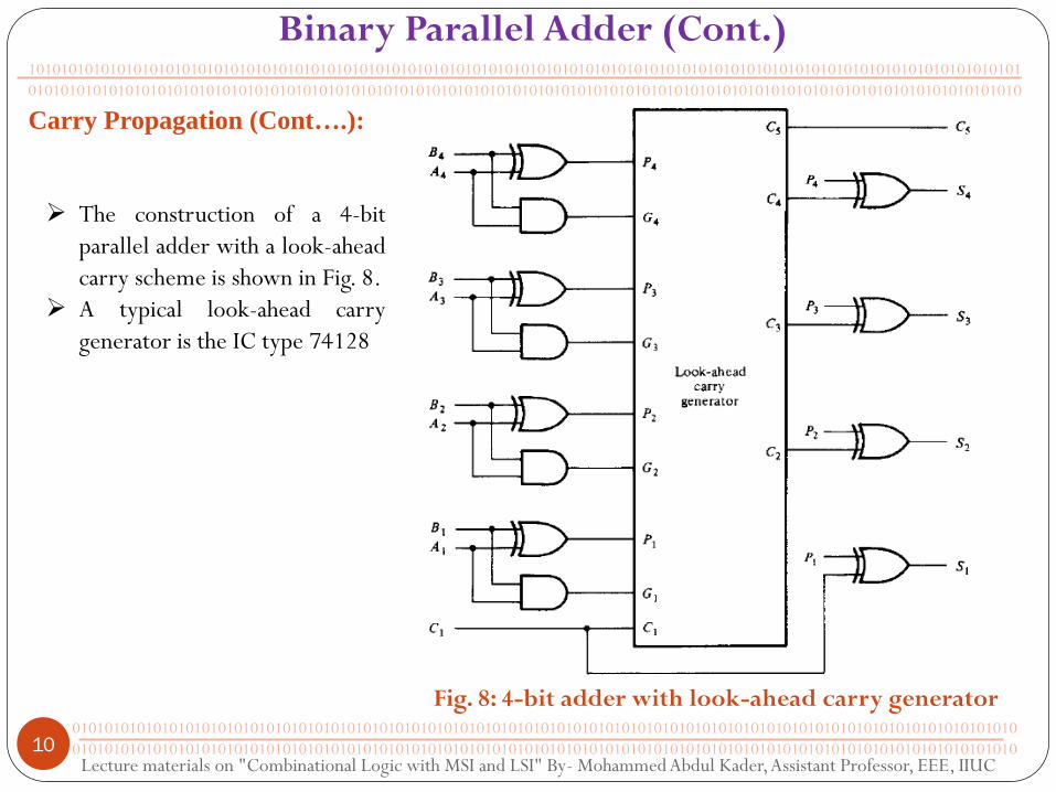
Carry Propagation (Cont….):
Binary Parallel Adder (Cont.)
Fig. 8: 4-bit adder with look-ahead carry generator
The construction of a 4-bit
parallel adder with a look-ahead
carry scheme is shown in Fig. 8.
A typical look-ahead carry
generator is the IC type 74128
Lecture materials on "Combinational Logic with MSI and LSI" By- Mohammed Abdul Kader, Assistant Professor, EEE, IIUC 11
101010101010101010101010101010101010101010101010101010101010101010101010101010101010101010101010101010101010101010101010101
010101010101010101010101010101010101010101010101010101010101010101010101010101010101010101010101010101010101010101010101010
010101010101010101010101010101010101010101010101010101010101010101010101010101010101010101010101010101010101010101010
010101010101010101010101010101010101010101010101010101010101010101010101010101010101010101010101010101010101010101010
BCD Adder
A BCD adder is a circuit that adds two BCD digits in parallel and produces a sum digital
so in BCD.
Consider the arithmetic addition of two decimal digits in BCD, together with a previous
carry from a previous stage. The output sum cannot be greater than 9+9+1=19, the 1 in
the sum being an input carry.
Suppose, we apply two BCD digits to a 4-bit binary adder. The adder will form the sum
in binary and produce a result which may range from 0 to19.

Lecture materials on "Combinational Logic with MSI and LSI" By- Mohammed Abdul Kader, Assistant Professor, EEE, IIUC 12
101010101010101010101010101010101010101010101010101010101010101010101010101010101010101010101010101010101010101010101010101
010101010101010101010101010101010101010101010101010101010101010101010101010101010101010101010101010101010101010101010101010
010101010101010101010101010101010101010101010101010101010101010101010101010101010101010101010101010101010101010101010
010101010101010101010101010101010101010101010101010101010101010101010101010101010101010101010101010101010101010101010
BCD Adder
In examining the content of the table, it is apparent that when the binary sum is equal to or less
than1001,the corresponding BCD number is identical, and therefore no conversion is needed.
When the binary sum is
greater than 1001,we
obtain a non-valid BCD
representation. The
addition of binary 0110
(6 in decimal) to the
binary sum converts it to
the correct BCD
representation and also
produces an output carry.
The condition for a
correction and an output
carry can be expressed by
the Boolean function:

Lecture materials on "Combinational Logic with MSI and LSI" By- Mohammed Abdul Kader, Assistant Professor, EEE, IIUC 13
101010101010101010101010101010101010101010101010101010101010101010101010101010101010101010101010101010101010101010101010101
010101010101010101010101010101010101010101010101010101010101010101010101010101010101010101010101010101010101010101010101010
010101010101010101010101010101010101010101010101010101010101010101010101010101010101010101010101010101010101010101010
010101010101010101010101010101010101010101010101010101010101010101010101010101010101010101010101010101010101010101010
BCD Adder
C
C=0, when binary sum is less or
equal to 1001. In this case binary
sum and BCD sum are same. So,
nothing is added to the binary
sum.
C=1, when binary sum is greater
than 1001. binary 0110 is added
to the binary sum through the
bottom 4-bit binary adder to
convert the binary sum into BCD
sum.
Fig. 9: Block diagram of a BCD adder

Lecture materials on "Combinational Logic with MSI and LSI" By- Mohammed Abdul Kader, Assistant Professor, EEE, IIUC 14
101010101010101010101010101010101010101010101010101010101010101010101010101010101010101010101010101010101010101010101010101
010101010101010101010101010101010101010101010101010101010101010101010101010101010101010101010101010101010101010101010101010
010101010101010101010101010101010101010101010101010101010101010101010101010101010101010101010101010101010101010101010
010101010101010101010101010101010101010101010101010101010101010101010101010101010101010101010101010101010101010101010
Magnitude Comparator
A magnitude comparator is a combinational circuit that compares two numbers A & B
and determines the irrelative magnitudes. The outcome of the comparison is specified by
three binary variables that indicate whether A>B,A=B,or A<B.
Consider two numbers A and B with four digits each.
𝐴 = 𝐴3𝐴2𝐴1𝐴0
𝐵 = 𝐵3𝐵2𝐵1𝐵0
The two numbers are equal if all pairs of significant digits are equal i.e. 𝐴3=𝐵3 and 𝐴2=𝐵2
and 𝐴1=𝐵1 and 𝐴0=𝐵0.
The equality relation of each pair of bits can be expressed:
𝑥𝑖 = 𝐴𝑖𝐵𝑖 + 𝐴𝑖 𝐵𝑖
, i=0,1,2,3
Where 𝑥𝑖 = 1 only if the pair of bits in position, i , are equal, i.e. if both are 1’s or both are
0’s.

Lecture materials on "Combinational Logic with MSI and LSI" By- Mohammed Abdul Kader, Assistant Professor, EEE, IIUC 15
101010101010101010101010101010101010101010101010101010101010101010101010101010101010101010101010101010101010101010101010101
010101010101010101010101010101010101010101010101010101010101010101010101010101010101010101010101010101010101010101010101010
010101010101010101010101010101010101010101010101010101010101010101010101010101010101010101010101010101010101010101010
010101010101010101010101010101010101010101010101010101010101010101010101010101010101010101010101010101010101010101010
Magnitude Comparator (Cont.)
For equity condition to exist, all 𝑥𝑖 variables must be equal to 1.
(A=B) = 𝑥3𝑥2𝑥1𝑥0
A and B will be equal if 𝑥3 = 𝑥2 = 𝑥1=𝑥0 = 1 or, all pairs of digits of the two numbers are
equal.
To determine if A is greater than or less than B, we inspect the relative magnitude of pairs
of significant digits starting from most significant position. If the two digits are equal, we
compare the next lower significant pair of digits. This comparison continues until a pair of
unique digits is reached. If the digit of A is 1 and that of B is 0, we conclude A>B. If the
corresponding digit of A is 0 and that of B is 1, we have that A<B.
Lecture materials on "Combinational Logic with MSI and LSI" By- Mohammed Abdul Kader, Assistant Professor, EEE, IIUC 16
101010101010101010101010101010101010101010101010101010101010101010101010101010101010101010101010101010101010101010101010101
010101010101010101010101010101010101010101010101010101010101010101010101010101010101010101010101010101010101010101010101010
010101010101010101010101010101010101010101010101010101010101010101010101010101010101010101010101010101010101010101010
010101010101010101010101010101010101010101010101010101010101010101010101010101010101010101010101010101010101010101010
Magnitude Comparator (Cont.)
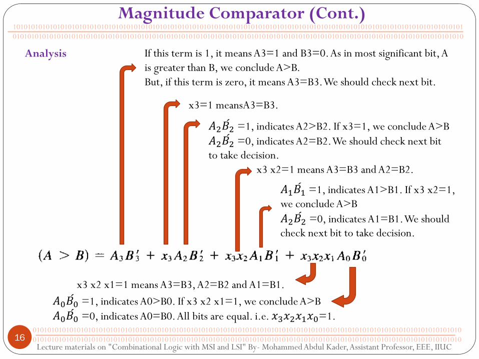
Analysis If this term is 1, it means A3=1 and B3=0. As in most significant bit, A
is greater than B, we conclude A>B.
But, if this term is zero, it means A3=B3. We should check next bit.
x3=1 meansA3=B3.
𝐴2𝐵2 =1, indicates A2>B2. If x3=1, we conclude A>B
𝐴2𝐵2 =0, indicates A2=B2. We should check next bit
to take decision.
x3 x2=1 means A3=B3 and A2=B2.
𝐴1𝐵1 =1, indicates A1>B1. If x3 x2=1,
we conclude A>B
𝐴2𝐵2 =0, indicates A1=B1. We should
check next bit to take decision.
x3 x2 x1=1 means A3=B3, A2=B2 and A1=B1.
𝐴0𝐵0 =1, indicates A0>B0. If x3 x2 x1=1, we conclude A>B
𝐴0𝐵0 =0, indicates A0=B0. All bits are equal. i.e. 𝑥3𝑥2𝑥1𝑥0=1.
Lecture materials on "Combinational Logic with MSI and LSI" By- Mohammed Abdul Kader, Assistant Professor, EEE, IIUC 17
101010101010101010101010101010101010101010101010101010101010101010101010101010101010101010101010101010101010101010101010101
010101010101010101010101010101010101010101010101010101010101010101010101010101010101010101010101010101010101010101010101010
010101010101010101010101010101010101010101010101010101010101010101010101010101010101010101010101010101010101010101010
010101010101010101010101010101010101010101010101010101010101010101010101010101010101010101010101010101010101010101010
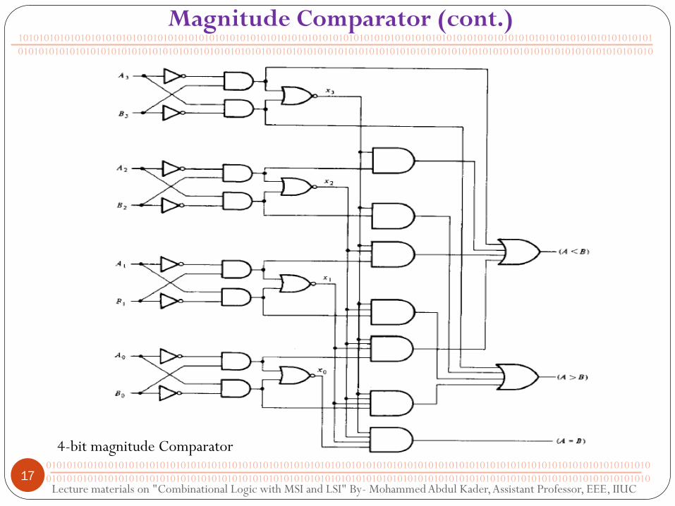
Magnitude Comparator (cont.)
4-bit magnitude Comparator
Lecture materials on "Combinational Logic with MSI and LSI" By- Mohammed Abdul Kader, Assistant Professor, EEE, IIUC 18
101010101010101010101010101010101010101010101010101010101010101010101010101010101010101010101010101010101010101010101010101
010101010101010101010101010101010101010101010101010101010101010101010101010101010101010101010101010101010101010101010101010
010101010101010101010101010101010101010101010101010101010101010101010101010101010101010101010101010101010101010101010
010101010101010101010101010101010101010101010101010101010101010101010101010101010101010101010101010101010101010101010
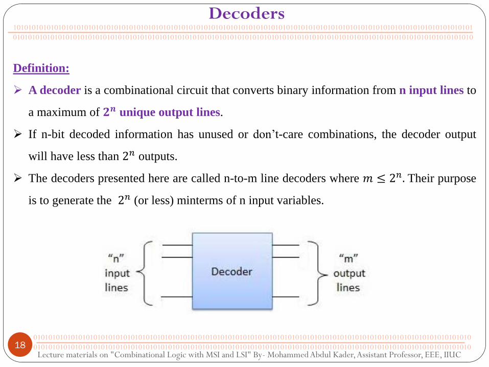
Decoders
Definition:
A decoder is a combinational circuit that converts binary information from n input lines to
a maximum of 𝟐𝒏 unique output lines.
If n-bit decoded information has unused or don’t-care combinations, the decoder output
will have less than 2𝑛 outputs.
The decoders presented here are called n-to-m line decoders where 𝑚 ≤ 2𝑛. Their purpose
is to generate the 2𝑛 (or less) minterms of n input variables.

Lecture materials on "Combinational Logic with MSI and LSI" By- Mohammed Abdul Kader, Assistant Professor, EEE, IIUC 19
101010101010101010101010101010101010101010101010101010101010101010101010101010101010101010101010101010101010101010101010101
010101010101010101010101010101010101010101010101010101010101010101010101010101010101010101010101010101010101010101010101010
010101010101010101010101010101010101010101010101010101010101010101010101010101010101010101010101010101010101010101010
010101010101010101010101010101010101010101010101010101010101010101010101010101010101010101010101010101010101010101010
Decoders
Application:
Decoders are greatly used in applications where the particular output or group of outputs to be
activated only on the occurrence of a specific combination of input levels. Some important
application of decoder circuit is given below-
Address Decoders: Amongst its many uses, a decoder is widely used to decode the
particular memory location in the computer memory system. Decoders accept the address
code generated by the CPU which is a combination of address bits for a specific location in
the memory.
Instruction Decoder: Another application of the decoder can be found in the control unit
of the central processing unit. This decoder is used to decode the program instructions in
order to activate the specific control lines such that different operations in the ALU of the
CPU are carried out.
Lecture materials on "Combinational Logic with MSI and LSI" By- Mohammed Abdul Kader, Assistant Professor, EEE, IIUC 20
101010101010101010101010101010101010101010101010101010101010101010101010101010101010101010101010101010101010101010101010101
010101010101010101010101010101010101010101010101010101010101010101010101010101010101010101010101010101010101010101010101010
010101010101010101010101010101010101010101010101010101010101010101010101010101010101010101010101010101010101010101010
010101010101010101010101010101010101010101010101010101010101010101010101010101010101010101010101010101010101010101010
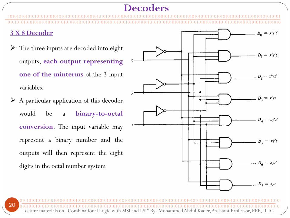
Decoders
3 X 8 Decoder
The three inputs are decoded into eight
outputs, each output representing
one of the minterms of the 3-input
variables.
A particular application of this decoder
would be a binary-to-octal
conversion. The input variable may
represent a binary number and the
outputs will then represent the eight
digits in the octal number system

Lecture materials on "Combinational Logic with MSI and LSI" By- Mohammed Abdul Kader, Assistant Professor, EEE, IIUC 21
101010101010101010101010101010101010101010101010101010101010101010101010101010101010101010101010101010101010101010101010101
010101010101010101010101010101010101010101010101010101010101010101010101010101010101010101010101010101010101010101010101010
010101010101010101010101010101010101010101010101010101010101010101010101010101010101010101010101010101010101010101010
010101010101010101010101010101010101010101010101010101010101010101010101010101010101010101010101010101010101010101010
Decoders
Truth Table of 3 X 8 line decoder
From the truth table it is observed that the output variables are mutually exclusive because only one
output can be equal to 1 at any one time. The output line whose value is equal to 1 represents the
minterm equivalent of the binary number presently available in the input lines.

Lecture materials on "Combinational Logic with MSI and LSI" By- Mohammed Abdul Kader, Assistant Professor, EEE, IIUC 22
101010101010101010101010101010101010101010101010101010101010101010101010101010101010101010101010101010101010101010101010101
010101010101010101010101010101010101010101010101010101010101010101010101010101010101010101010101010101010101010101010101010
010101010101010101010101010101010101010101010101010101010101010101010101010101010101010101010101010101010101010101010
010101010101010101010101010101010101010101010101010101010101010101010101010101010101010101010101010101010101010101010
Decoders
Example 5-2: Design a BCD-to-decimal decoder
Lecture materials on "Combinational Logic with MSI and LSI" By- Mohammed Abdul Kader, Assistant Professor, EEE, IIUC 23
101010101010101010101010101010101010101010101010101010101010101010101010101010101010101010101010101010101010101010101010101
010101010101010101010101010101010101010101010101010101010101010101010101010101010101010101010101010101010101010101010101010
010101010101010101010101010101010101010101010101010101010101010101010101010101010101010101010101010101010101010101010
010101010101010101010101010101010101010101010101010101010101010101010101010101010101010101010101010101010101010101010
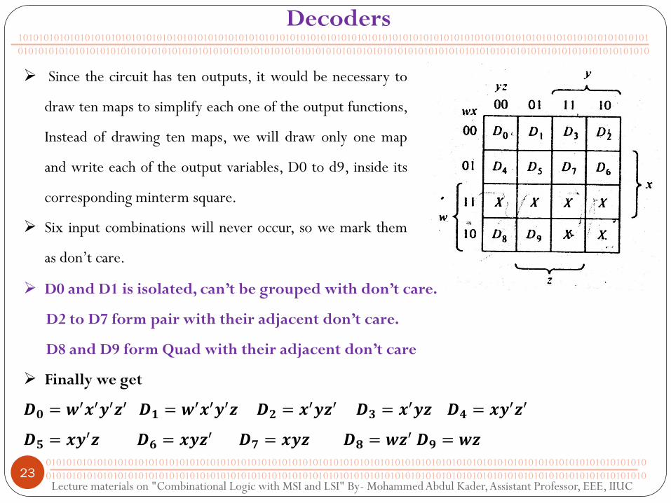
Decoders
Since the circuit has ten outputs, it would be necessary to
draw ten maps to simplify each one of the output functions,
Instead of drawing ten maps, we will draw only one map
and write each of the output variables, D0 to d9, inside its
corresponding minterm square.
Six input combinations will never occur, so we mark them
as don’t care.
D0 and D1 is isolated, can’t be grouped with don’t care.
D2 to D7 form pair with their adjacent don’t care.
D8 and D9 form Quad with their adjacent don’t care
Finally we get
𝑫𝟎 = 𝒘′𝒙′𝒚′𝒛′ 𝑫𝟏 = 𝒘′𝒙′𝒚′𝒛 𝑫𝟐 = 𝒙′𝒚𝒛′ 𝑫𝟑 = 𝒙′𝒚𝒛 𝑫𝟒 = 𝒙𝒚′𝒛′
𝑫𝟓 = 𝒙𝒚′𝒛 𝑫𝟔 = 𝒙𝒚𝒛′ 𝑫𝟕 = 𝒙𝒚𝒛 𝑫𝟖 = 𝒘𝒛′ 𝑫𝟗 = 𝒘𝒛
Lecture materials on "Combinational Logic with MSI and LSI" By- Mohammed Abdul Kader, Assistant Professor, EEE, IIUC 24
101010101010101010101010101010101010101010101010101010101010101010101010101010101010101010101010101010101010101010101010101
010101010101010101010101010101010101010101010101010101010101010101010101010101010101010101010101010101010101010101010101010
010101010101010101010101010101010101010101010101010101010101010101010101010101010101010101010101010101010101010101010
010101010101010101010101010101010101010101010101010101010101010101010101010101010101010101010101010101010101010101010
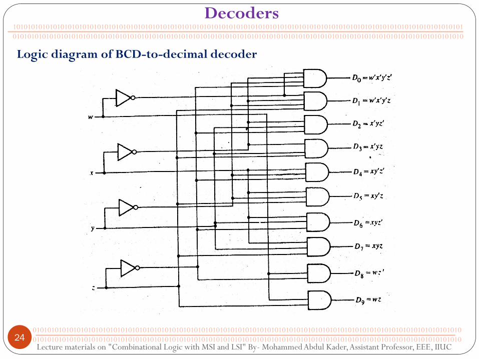
Decoders
Logic diagram of BCD-to-decimal decoder
Lecture materials on "Combinational Logic with MSI and LSI" By- Mohammed Abdul Kader, Assistant Professor, EEE, IIUC 25
101010101010101010101010101010101010101010101010101010101010101010101010101010101010101010101010101010101010101010101010101
010101010101010101010101010101010101010101010101010101010101010101010101010101010101010101010101010101010101010101010101010
010101010101010101010101010101010101010101010101010101010101010101010101010101010101010101010101010101010101010101010
010101010101010101010101010101010101010101010101010101010101010101010101010101010101010101010101010101010101010101010
Decoders
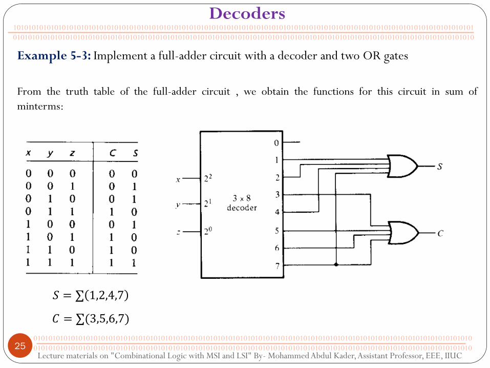
Example 5-3: Implement a full-adder circuit with a decoder and two OR gates
From the truth table of the full-adder circuit , we obtain the functions for this circuit in sum of
minterms:
𝑆 = ∑ 1,2,4,7
𝐶 = ∑(3,5,6,7)

Lecture materials on "Combinational Logic with MSI and LSI" By- Mohammed Abdul Kader, Assistant Professor, EEE, IIUC 26
101010101010101010101010101010101010101010101010101010101010101010101010101010101010101010101010101010101010101010101010101
010101010101010101010101010101010101010101010101010101010101010101010101010101010101010101010101010101010101010101010101010
010101010101010101010101010101010101010101010101010101010101010101010101010101010101010101010101010101010101010101010
010101010101010101010101010101010101010101010101010101010101010101010101010101010101010101010101010101010101010101010
Encoders
An encoder is a digital function that produces a reverse operation from that of a decoder. An encoder
has 𝟐𝒏 input lines and n output lines.
The output lines generate the binary code corresponding to the input value.
Example: Octal to binary encoder which has 8 inputs and 3 outputs
Truth Table of binary to octal encoder.
From the truth table:
• Output bit z is 1 if octal
digit is odd.
• Output y is 1 for octal
digits 2,3,6 or 7.
• Output x is 1 for octal
digits 4,5,6, 0r 7.

Lecture materials on "Combinational Logic with MSI and LSI" By- Mohammed Abdul Kader, Assistant Professor, EEE, IIUC 27
101010101010101010101010101010101010101010101010101010101010101010101010101010101010101010101010101010101010101010101010101
010101010101010101010101010101010101010101010101010101010101010101010101010101010101010101010101010101010101010101010101010
010101010101010101010101010101010101010101010101010101010101010101010101010101010101010101010101010101010101010101010
010101010101010101010101010101010101010101010101010101010101010101010101010101010101010101010101010101010101010101010
Encoders
Fig. Octal to binary encoder
Boolean function of output variables

Lecture materials on "Combinational Logic with MSI and LSI" By- Mohammed Abdul Kader, Assistant Professor, EEE, IIUC 28
101010101010101010101010101010101010101010101010101010101010101010101010101010101010101010101010101010101010101010101010101
010101010101010101010101010101010101010101010101010101010101010101010101010101010101010101010101010101010101010101010101010
010101010101010101010101010101010101010101010101010101010101010101010101010101010101010101010101010101010101010101010
010101010101010101010101010101010101010101010101010101010101010101010101010101010101010101010101010101010101010101010
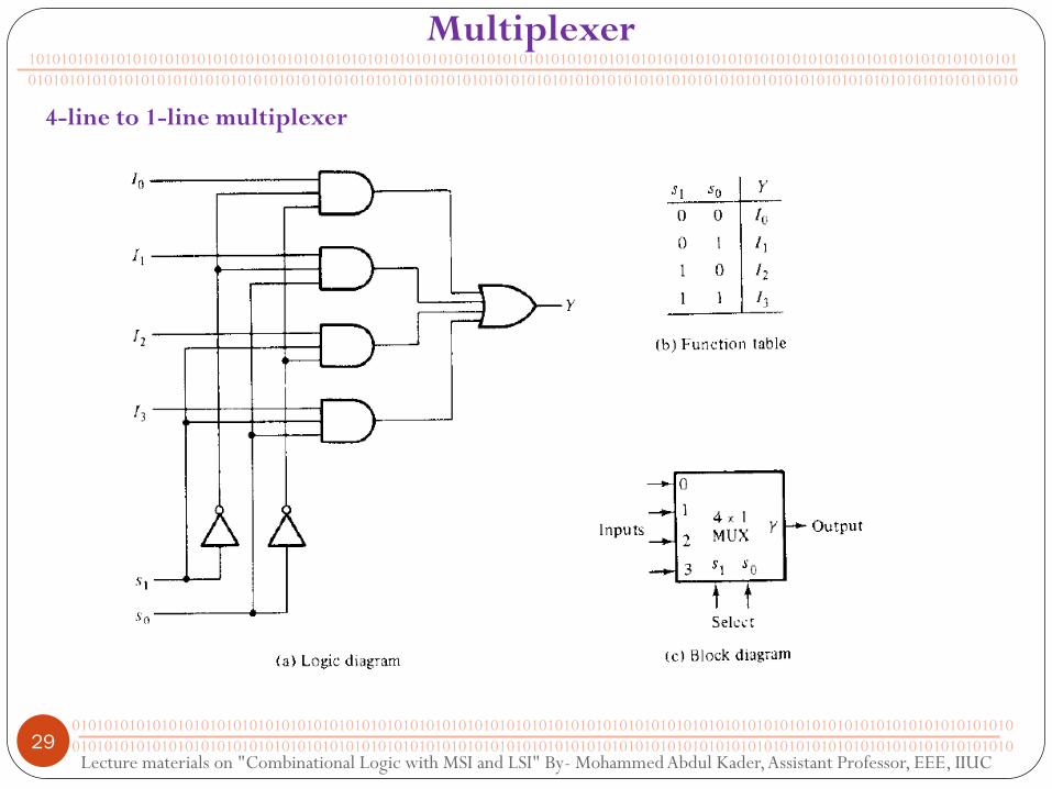
Multiplexer
Multiplexer means transmitting a large number of information units over a smaller number of
channels or lines.
A digital multiplexer is a combinational circuit that selects binary information from one of many
input lines and directs it to a single output line.
The selection of a particular input lines is controlled by a set of selection lines. Normally there are
𝟐𝒏 input lines and n selection lines whose bit combinations determine which input is selected.
A multiplexer is also called a data selector, since it selects one of many inputs and steers the binary
information to the output line.
𝟐𝒏 input lines
n selection lines
1 output line Multiplexer
Lecture materials on "Combinational Logic with MSI and LSI" By- Mohammed Abdul Kader, Assistant Professor, EEE, IIUC 29
101010101010101010101010101010101010101010101010101010101010101010101010101010101010101010101010101010101010101010101010101
010101010101010101010101010101010101010101010101010101010101010101010101010101010101010101010101010101010101010101010101010
010101010101010101010101010101010101010101010101010101010101010101010101010101010101010101010101010101010101010101010
010101010101010101010101010101010101010101010101010101010101010101010101010101010101010101010101010101010101010101010
Multiplexer
4-line to 1-line multiplexer

Lecture materials on "Combinational Logic with MSI and LSI" By- Mohammed Abdul Kader, Assistant Professor, EEE, IIUC 30
101010101010101010101010101010101010101010101010101010101010101010101010101010101010101010101010101010101010101010101010101
010101010101010101010101010101010101010101010101010101010101010101010101010101010101010101010101010101010101010101010101010
010101010101010101010101010101010101010101010101010101010101010101010101010101010101010101010101010101010101010101010
010101010101010101010101010101010101010101010101010101010101010101010101010101010101010101010101010101010101010101010
Multiplexer
Implementation of Boolean function F(𝐀, 𝐁, 𝐂) = ∑ 𝟏, 𝟑, 𝟓, 𝟔 by multiplexer

Lecture materials on "Combinational Logic with MSI and LSI" By- Mohammed Abdul Kader, Assistant Professor, EEE, IIUC 31
101010101010101010101010101010101010101010101010101010101010101010101010101010101010101010101010101010101010101010101010101
010101010101010101010101010101010101010101010101010101010101010101010101010101010101010101010101010101010101010101010101010
010101010101010101010101010101010101010101010101010101010101010101010101010101010101010101010101010101010101010101010
010101010101010101010101010101010101010101010101010101010101010101010101010101010101010101010101010101010101010101010
Multiplexer
Example 5-4:
Implementation of Boolean function F(𝐀, 𝐁, 𝐂, 𝐃) = ∑ 𝟎, 𝟏, 𝟑, 𝟒, 𝟖, 𝟗, 𝟏𝟓 by multiplexer
Lecture materials on "Combinational Logic with MSI and LSI" By- Mohammed Abdul Kader, Assistant Professor, EEE, IIUC 32
101010101010101010101010101010101010101010101010101010101010101010101010101010101010101010101010101010101010101010101010101
010101010101010101010101010101010101010101010101010101010101010101010101010101010101010101010101010101010101010101010101010
010101010101010101010101010101010101010101010101010101010101010101010101010101010101010101010101010101010101010101010
010101010101010101010101010101010101010101010101010101010101010101010101010101010101010101010101010101010101010101010
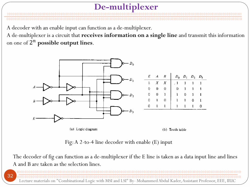
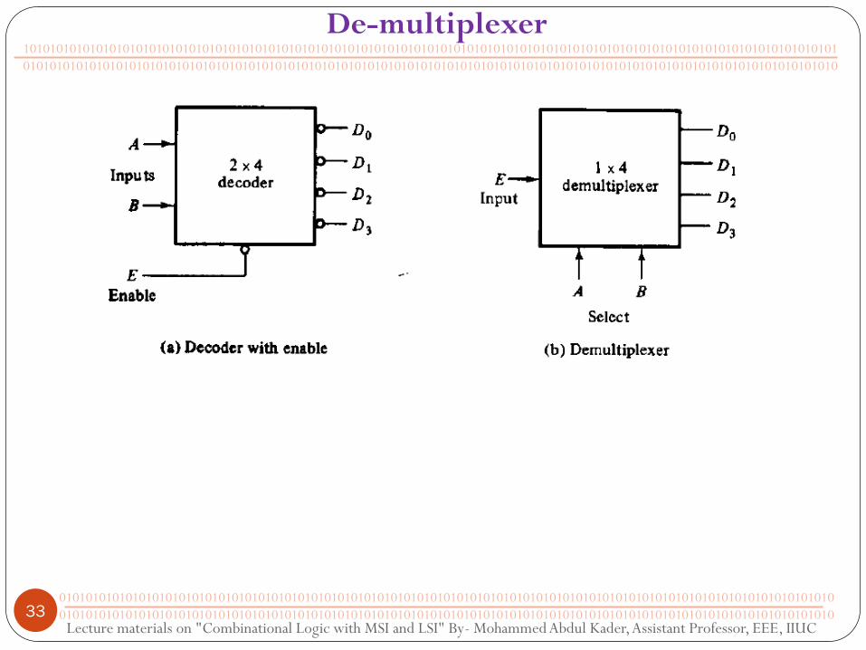
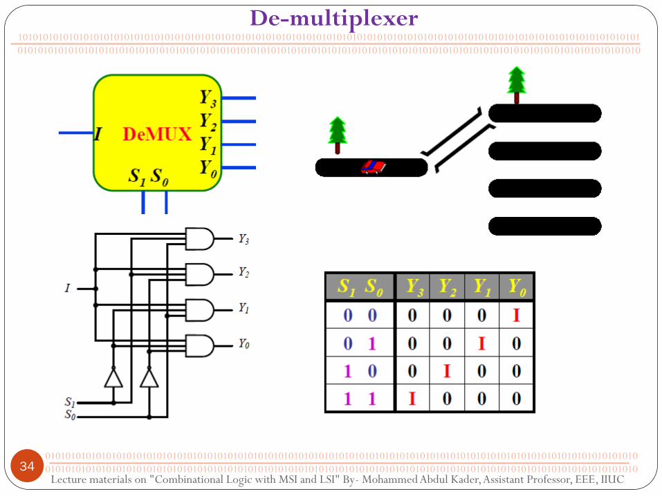
De-multiplexer
A decoder with an enable input can function as a de-multiplexer.
A de-multiplexer is a circuit that receives information on a single line and transmit this information
on one of 2𝑛 possible output lines.
Fig: A 2-to-4 line decoder with enable (E) input
The decoder of fig can function as a de-multiplexer if the E line is taken as a data input line and lines
A and B are taken as the selection lines.
Lecture materials on "Combinational Logic with MSI and LSI" By- Mohammed Abdul Kader, Assistant Professor, EEE, IIUC 33
101010101010101010101010101010101010101010101010101010101010101010101010101010101010101010101010101010101010101010101010101
010101010101010101010101010101010101010101010101010101010101010101010101010101010101010101010101010101010101010101010101010
010101010101010101010101010101010101010101010101010101010101010101010101010101010101010101010101010101010101010101010
010101010101010101010101010101010101010101010101010101010101010101010101010101010101010101010101010101010101010101010
De-multiplexer
Lecture materials on "Combinational Logic with MSI and LSI" By- Mohammed Abdul Kader, Assistant Professor, EEE, IIUC 34
101010101010101010101010101010101010101010101010101010101010101010101010101010101010101010101010101010101010101010101010101
010101010101010101010101010101010101010101010101010101010101010101010101010101010101010101010101010101010101010101010101010
010101010101010101010101010101010101010101010101010101010101010101010101010101010101010101010101010101010101010101010
010101010101010101010101010101010101010101010101010101010101010101010101010101010101010101010101010101010101010101010
De-multiplexer
Lecture materials on "Combinational Logic with MSI and LSI" By- Mohammed Abdul Kader, Assistant Professor, EEE, IIUC 35
101010101010101010101010101010101010101010101010101010101010101010101010101010101010101010101010101010101010101010101010101
010101010101010101010101010101010101010101010101010101010101010101010101010101010101010101010101010101010101010101010101010
010101010101010101010101010101010101010101010101010101010101010101010101010101010101010101010101010101010101010101010
010101010101010101010101010101010101010101010101010101010101010101010101010101010101010101010101010101010101010101010
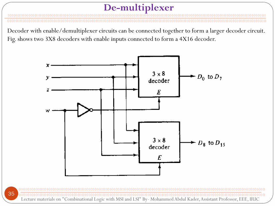
De-multiplexer
Decoder with enable/demultiplexer circuits can be connected together to form a larger decoder circuit.
Fig. shows two 3X8 decoders with enable inputs connected to form a 4X16 decoder.

Lecture materials on "Combinational Logic with MSI and LSI" By- Mohammed Abdul Kader, Assistant Professor, EEE, IIUC 36
101010101010101010101010101010101010101010101010101010101010101010101010101010101010101010101010101010101010101010101010101
010101010101010101010101010101010101010101010101010101010101010101010101010101010101010101010101010101010101010101010101010
010101010101010101010101010101010101010101010101010101010101010101010101010101010101010101010101010101010101010101010
010101010101010101010101010101010101010101010101010101010101010101010101010101010101010101010101010101010101010101010
Read-Only Memory (ROM)
A decoder generates the 𝟐𝒏 minterms of the n input variable. By inserting OR gates to sum
the minterms of Boolean functions, we are able to generate any desired combinational
circuit.
A read-only memory (ROM) is a device that includes both the decoder and the OR
gates within a single IC package. The connections between the outputs of the decoder and
the inputs of the OR gates can be specified for each particular configuration by
“programming” the ROM.
A ROM is essentially a memory (or storage) device in which a fixed set of binary
information is stored.
The binary information must first be specified by the user and is then embedded in the unit
to form the required interconnection pattern. ROM’s come with special internal links that
can be fused or broken. The desired interconnection for a particular application requires
that certain links be fused to form the required circuit paths. Once a pattern is established
for a ROM, it remain fixed even when power is turned off and then on again.

Lecture materials on "Combinational Logic with MSI and LSI" By- Mohammed Abdul Kader, Assistant Professor, EEE, IIUC 37
101010101010101010101010101010101010101010101010101010101010101010101010101010101010101010101010101010101010101010101010101
010101010101010101010101010101010101010101010101010101010101010101010101010101010101010101010101010101010101010101010101010
010101010101010101010101010101010101010101010101010101010101010101010101010101010101010101010101010101010101010101010
010101010101010101010101010101010101010101010101010101010101010101010101010101010101010101010101010101010101010101010
Read-Only Memory (ROM)
A ROM consists of n input lines and m output lines.
Each bit combination of input variables is called an address.
Each bit combination that comes out of the output lines is called a word. The number of
bits per word is equal to the number of output lines m.
A ROM with n input lines has 2𝑛distinct addresses, so there are 2𝑛distinct words which are
said to be stored in the unit.

Lecture materials on "Combinational Logic with MSI and LSI" By- Mohammed Abdul Kader, Assistant Professor, EEE, IIUC 38
101010101010101010101010101010101010101010101010101010101010101010101010101010101010101010101010101010101010101010101010101
010101010101010101010101010101010101010101010101010101010101010101010101010101010101010101010101010101010101010101010101010
010101010101010101010101010101010101010101010101010101010101010101010101010101010101010101010101010101010101010101010
010101010101010101010101010101010101010101010101010101010101010101010101010101010101010101010101010101010101010101010
Read-Only Memory (ROM)
Internally, the ROM is a combinational circuit with AND gates connected as a decoder and a number of OR
gates equal to the number of outputs in the unit. Figure shows the logic construction of a 32X4 ROM.
Lecture materials on "Combinational Logic with MSI and LSI" By- Mohammed Abdul Kader, Assistant Professor, EEE, IIUC 39
101010101010101010101010101010101010101010101010101010101010101010101010101010101010101010101010101010101010101010101010101
010101010101010101010101010101010101010101010101010101010101010101010101010101010101010101010101010101010101010101010101010
010101010101010101010101010101010101010101010101010101010101010101010101010101010101010101010101010101010101010101010
010101010101010101010101010101010101010101010101010101010101010101010101010101010101010101010101010101010101010101010
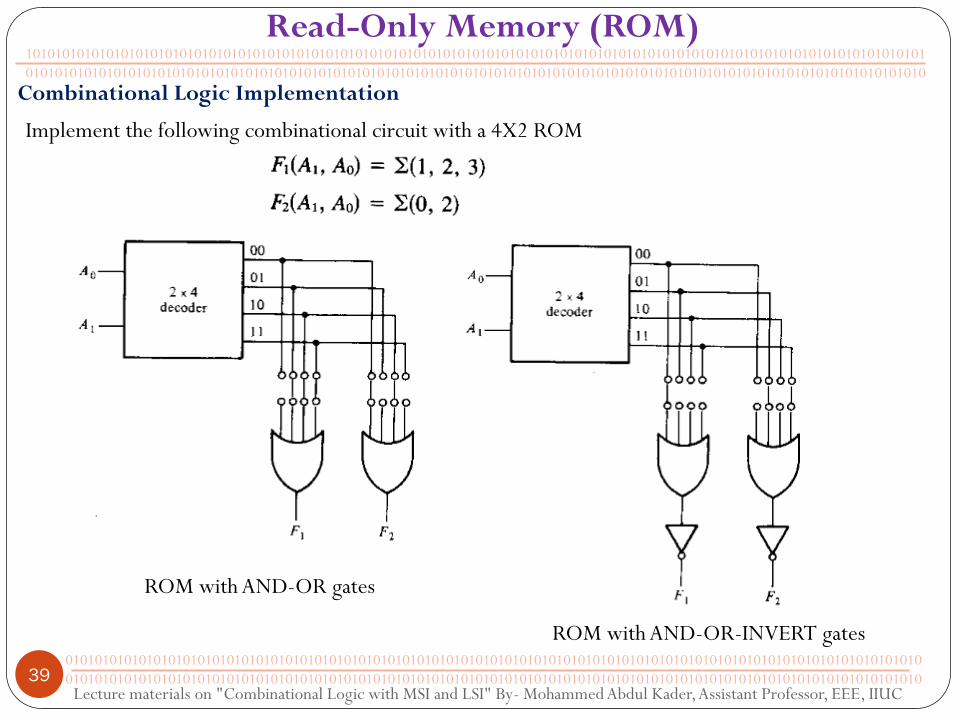
Read-Only Memory (ROM)
Combinational Logic Implementation
Implement the following combinational circuit with a 4X2 ROM
ROM with AND-OR gates
ROM with AND-OR-INVERT gates
Lecture materials on "Combinational Logic with MSI and LSI" By- Mohammed Abdul Kader, Assistant Professor, EEE, IIUC 40
101010101010101010101010101010101010101010101010101010101010101010101010101010101010101010101010101010101010101010101010101
010101010101010101010101010101010101010101010101010101010101010101010101010101010101010101010101010101010101010101010101010
010101010101010101010101010101010101010101010101010101010101010101010101010101010101010101010101010101010101010101010
010101010101010101010101010101010101010101010101010101010101010101010101010101010101010101010101010101010101010101010
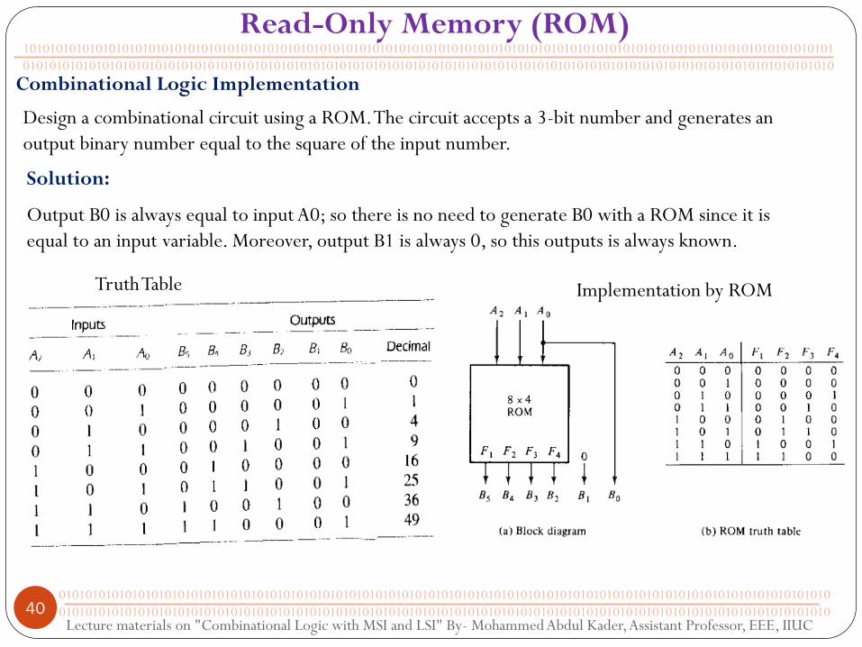
Read-Only Memory (ROM)
Combinational Logic Implementation
Design a combinational circuit using a ROM. The circuit accepts a 3-bit number and generates an
output binary number equal to the square of the input number.
Output B0 is always equal to input A0; so there is no need to generate B0 with a ROM since it is
equal to an input variable. Moreover, output B1 is always 0, so this outputs is always known.
Solution:
Truth Table Implementation by ROM

Lecture materials on "Combinational Logic with MSI and LSI" By- Mohammed Abdul Kader, Assistant Professor, EEE, IIUC 41
101010101010101010101010101010101010101010101010101010101010101010101010101010101010101010101010101010101010101010101010101
010101010101010101010101010101010101010101010101010101010101010101010101010101010101010101010101010101010101010101010101010
010101010101010101010101010101010101010101010101010101010101010101010101010101010101010101010101010101010101010101010
010101010101010101010101010101010101010101010101010101010101010101010101010101010101010101010101010101010101010101010
Programmable Logic Array (PLA)
Why PLA?
A combinational circuit may occasionally have don’t care conditions. When implemented
with a ROM, a don’t care condition becomes an address input that will never occur. The
words at the don’t care addresses need not be programmed and may be left in their original
state (all 0’s or all 1’s). The result is that not all the bit patterns available in the ROM are
used, which may be considered as waste of available equipment.
For example, a combinational circuit that converts a 12-bit card code to a 6-bit internal
alphanumeric code.
* It consists 12 inputs and 6 outputs. The size of the ROM must be 4096 X 6 (212 X 6).
* There are only 47 valid entries for the card code, all other input combinations are
don’t care. The remaining 4049 words of ROM are not used and are thus wasted.
So, for cases where the number of don’t care conditions is excessive, it is more
economical to use a second type of LSI component called Programmable Logic Array
(PLA).

Lecture materials on "Combinational Logic with MSI and LSI" By- Mohammed Abdul Kader, Assistant Professor, EEE, IIUC 42
101010101010101010101010101010101010101010101010101010101010101010101010101010101010101010101010101010101010101010101010101
010101010101010101010101010101010101010101010101010101010101010101010101010101010101010101010101010101010101010101010101010
010101010101010101010101010101010101010101010101010101010101010101010101010101010101010101010101010101010101010101010
010101010101010101010101010101010101010101010101010101010101010101010101010101010101010101010101010101010101010101010
Programmable Logic Array (PLA)
PLA does not provide full decoding of the variables and does not generate all the minterms
as in the ROM.
A block diagram is shown in fig. It consists n inputs, m-outputs, k product terms and m
sum terms. The product terms constitute a group of k AND gates and the sum terms
constitute a group of m OR gates.
Links between all n inputs and
their complement values to each
of the AND gates.
2n X k links
Links between outputs of the
AND gates and the inputs of
the OR gates.
k X m links
Links to generate AND-
OR form or, AND-OR-
INVERT form
m links
The number of programmed links is 2n X k + k X m +m, whereas that of a ROM is 2𝑛𝑋 𝑚

Lecture materials on "Combinational Logic with MSI and LSI" By- Mohammed Abdul Kader, Assistant Professor, EEE, IIUC 43
101010101010101010101010101010101010101010101010101010101010101010101010101010101010101010101010101010101010101010101010101
010101010101010101010101010101010101010101010101010101010101010101010101010101010101010101010101010101010101010101010101010
010101010101010101010101010101010101010101010101010101010101010101010101010101010101010101010101010101010101010101010
010101010101010101010101010101010101010101010101010101010101010101010101010101010101010101010101010101010101010101010
Programmable Logic Array (PLA)
Implementation of combinational circuit by PLA.
Lecture materials on "Combinational Logic with MSI and LSI" By- Mohammed Abdul Kader, Assistant Professor, EEE, IIUC 44
101010101010101010101010101010101010101010101010101010101010101010101010101010101010101010101010101010101010101010101010101
010101010101010101010101010101010101010101010101010101010101010101010101010101010101010101010101010101010101010101010101010
010101010101010101010101010101010101010101010101010101010101010101010101010101010101010101010101010101010101010101010
010101010101010101010101010101010101010101010101010101010101010101010101010101010101010101010101010101010101010101010
Programmable Logic Array (PLA)
PLA Types.
PLA may be mask-programmable or field programmable.
With a mask programmable PLA, the customer must submit a PLA program table to the
manufacturer. This table is used by the vendor to produce a custom-made PLA that has the
required internal paths between inputs and outputs.
A second type of PLA available is called field programmable logic array or FPLA. The
FPLA can be programmed by the user by means of certain recommended procedure.
Commercial hardware programmable units are available for use in conjunction with certain
FPLAs
Top Related