


Languages
Pages
Legal

DS573 April 19, 2010 www.xilinx.com 1Product Specification
© Copyright 2007-2010 Xilinx, Inc. XILINX, the Xilinx logo, Virtex, Spartan, ISE and other designated brands included herein are trademarks of Xilinx in the United States and other countries. All other trademarks are the property of their respective owners.
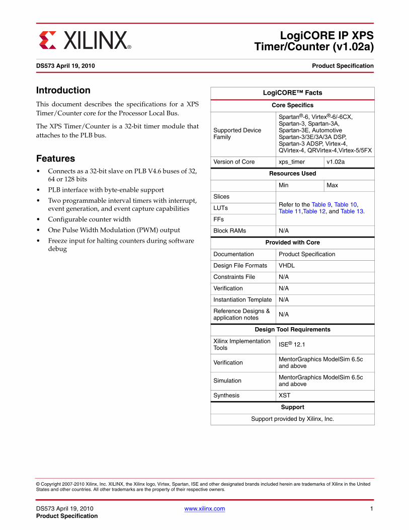
IntroductionThis document describes the specifications for a XPSTimer/Counter core for the Processor Local Bus.
The XPS Timer/Counter is a 32-bit timer module thatattaches to the PLB bus.
Features• Connects as a 32-bit slave on PLB V4.6 buses of 32,
64 or 128 bits
• PLB interface with byte-enable support
• Two programmable interval timers with interrupt, event generation, and event capture capabilities
• Configurable counter width
• One Pulse Width Modulation (PWM) output
• Freeze input for halting counters during software debug
0
LogiCORE IP XPSTimer/Counter (v1.02a)
DS573 April 19, 2010 0 0 Product Specification
LogiCORE™ Facts
Core Specifics
Supported Device Family
Spartan®-6, Virtex®-6/-6CX, Spartan-3, Spartan-3A, Spartan-3E, Automotive Spartan-3/3E/3A/3A DSP, Spartan-3 ADSP, Virtex-4, QVirtex-4, QRVirtex-4,Virtex-5/5FX
Version of Core xps_timer v1.02a
Resources Used
Min Max
SlicesRefer to the Table 9, Table 10, Table 11,Table 12, and Table 13.LUTs
FFs
Block RAMs N/A
Provided with Core
Documentation Product Specification
Design File Formats VHDL
Constraints File N/A
Verification N/A
Instantiation Template N/A
Reference Designs & application notes N/A
Design Tool Requirements
Xilinx Implementation Tools ISE® 12.1
Verification MentorGraphics ModelSim 6.5c and above
Simulation MentorGraphics ModelSim 6.5c and above
Synthesis XST
Support
Support provided by Xilinx, Inc.
DS573 April 19, 2010 www.xilinx.com 2Product Specification
LogiCORE IP XPS Timer/Counter (v1.02a)
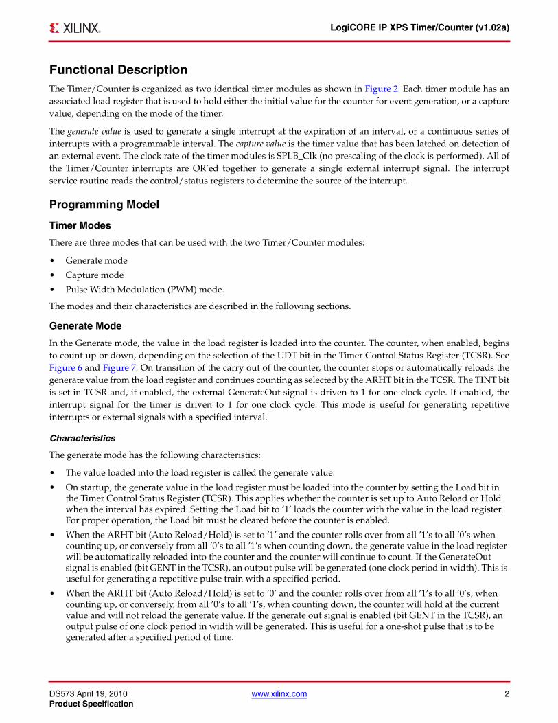
Functional DescriptionThe Timer/Counter is organized as two identical timer modules as shown in Figure 2. Each timer module has anassociated load register that is used to hold either the initial value for the counter for event generation, or a capturevalue, depending on the mode of the timer.
The generate value is used to generate a single interrupt at the expiration of an interval, or a continuous series ofinterrupts with a programmable interval. The capture value is the timer value that has been latched on detection ofan external event. The clock rate of the timer modules is SPLB_Clk (no prescaling of the clock is performed). All ofthe Timer/Counter interrupts are OR’ed together to generate a single external interrupt signal. The interruptservice routine reads the control/status registers to determine the source of the interrupt.
Programming Model
Timer Modes
There are three modes that can be used with the two Timer/Counter modules:
• Generate mode
• Capture mode
• Pulse Width Modulation (PWM) mode.
The modes and their characteristics are described in the following sections.
Generate Mode
In the Generate mode, the value in the load register is loaded into the counter. The counter, when enabled, beginsto count up or down, depending on the selection of the UDT bit in the Timer Control Status Register (TCSR). SeeFigure 6 and Figure 7. On transition of the carry out of the counter, the counter stops or automatically reloads thegenerate value from the load register and continues counting as selected by the ARHT bit in the TCSR. The TINT bitis set in TCSR and, if enabled, the external GenerateOut signal is driven to 1 for one clock cycle. If enabled, theinterrupt signal for the timer is driven to 1 for one clock cycle. This mode is useful for generating repetitiveinterrupts or external signals with a specified interval.
Characteristics
The generate mode has the following characteristics:
• The value loaded into the load register is called the generate value.
• On startup, the generate value in the load register must be loaded into the counter by setting the Load bit in the Timer Control Status Register (TCSR). This applies whether the counter is set up to Auto Reload or Hold when the interval has expired. Setting the Load bit to ’1’ loads the counter with the value in the load register. For proper operation, the Load bit must be cleared before the counter is enabled.
• When the ARHT bit (Auto Reload/Hold) is set to ’1’ and the counter rolls over from all ’1’s to all ’0’s when counting up, or conversely from all ’0’s to all ’1’s when counting down, the generate value in the load register will be automatically reloaded into the counter and the counter will continue to count. If the GenerateOut signal is enabled (bit GENT in the TCSR), an output pulse will be generated (one clock period in width). This is useful for generating a repetitive pulse train with a specified period.
• When the ARHT bit (Auto Reload/Hold) is set to ’0’ and the counter rolls over from all ’1’s to all ’0’s, when counting up, or conversely, from all ’0’s to all ’1’s, when counting down, the counter will hold at the current value and will not reload the generate value. If the generate out signal is enabled (bit GENT in the TCSR), an output pulse of one clock period in width will be generated. This is useful for a one-shot pulse that is to be generated after a specified period of time.
DS573 April 19, 2010 www.xilinx.com 3Product Specification
LogiCORE IP XPS Timer/Counter (v1.02a)
• The counter can be set up to count either up or down as determined by the selection of the UDT bit in the TCSR. If the counter is set up as a down counter, the generate value is the number of clocks in the timing interval. The period of the GenerateOut signal is the generate value times the clock period.
• When the counter is set to count down,
• TIMING_INTERVAL = (TLRx + 2) x PLB_CLOCK_PERIOD
• When the counter is set to count up,
• TIMING_INTERVAL = (MAX_COUNT - TLRx + 2) x PLB_CLOCK_PERIOD,
• where MAX_COUNT is the maximum count value of the counter, such as 0xFFFFFFFF for a 32-bit counter.
• The GenerateOut signals can be configured as high-true or low-true.
Capture Mode
In Capture Mode, the value of the counter is stored in the load register when the external capture signal is asserted.The TINT bit is also set in the Timer Control Status Register (TCSR) on detection of the capture event. The countercan be configured as an up or down counter for this mode as determined by the selection of the UDT bit in TCSR.The ARHT bit controls whether the capture value is overwritten with a new capture value before the previous TINTflag is cleared. This mode is useful for time tagging external events while simultaneously generating an interrupt.
Characteristics
Capture Mode has the following characteristics:
• The capture signal can be configured to be low-true or high-true.
• The capture signal is sampled within the Timer/Counter with the SPLB_Clk. The capture event is defined as the transition on the sampled signal to the asserted state. For example, if the capture signal is defined to be high-true, then the capture event is when the sampled signal, synchronized to the SPLB_Clk, transitions from ’0’ to ’1’.
• When the capture event occurs, the counter value is written to the load register. This value is called the capture value.
• When the ARHT bit (Auto Reload/Hold) is set to ’0’ and the capture event occurs, the capture value is written to the Load Register which holds the capture value until the load register is read. If the load register is not read, subsequent capture events will not update the load register, and will be lost.
• When the ARHT bit (Auto Reload/Hold) is set to ’1’, and the capture event occurs, the capture value is always written to the load register. Subsequent capture events will update the load register and will overwrite the previous value, whether it has been read or not.
• The counter can be set up to count either up or down as determined by the selection of the UDT bit in the Timer Control Status Register (TCSR).
Pulse Width Modulation (PWM) Mode
In PWM mode, two timer/counters are used as a pair to produce an output signal (PWM0) with a specifiedfrequency and duty factor. Timer0 sets the period and Timer1 sets the high time for the PWM0 output.
Characteristics
PWM Mode has the following characteristics:
• The mode for both Timer0 and TImer1 must be set to Generate Mode (bit MDT in the TCSR set to ’0’).
• The PWMA0 bit in TCSR0 and PWMB0 bit in TCSR1 must be set to ’1’ to enable PWM mode.
• The GenerateOut signals must be enabled in the TCSR (bit GENT set to ’1’). The PWM0 signal is generated from the GenerateOut signals of Timer0 and Timer1, so these signals must be enabled in both timer/counters.
DS573 April 19, 2010 www.xilinx.com 4Product Specification
LogiCORE IP XPS Timer/Counter (v1.02a)
• The assertion level of the GenerateOut signals for both timers in the pair must be set to ’1’. This is done by setting C_GEN0_ASSERT and C_GEN1_ASSERT to ’1’.
• The counter can be set to count up or down.
Setting the PWM Period and Duty Factor
The PWM period is determined by the generate value in Timer0’s load register (TLR0). The PWM high time isdetermined by the generate value in Timer1’s load register (TLR1). The period and duty factor are calculated asfollows:
When counters are configured to count up (UDT = ’0’):
PWM_PERIOD = (MAX_COUNT - TLR0 + 2) x PLB_CLOCK_PERIODPWM_HIGH_TIME = (MAX_COUNT - TLR1 + 2) x PLB_CLOCK_PERIOD
When counters are configured to count down (UDT = ’1’):
PWM_PERIOD = (TLR0 + 2) x PLB_CLOCK_PERIODPWM_HIGH_TIME = (TLR1 + 2) x PLB_CLOCK_PERIOD
where MAX_COUNT is the maximum count value for the counter, such as 0xFFFFFFFF for a 32-bit counter.
Interrupts
The TC interrupt signals can be enabled or disabled with the ENIT bit in the TCSR. The interrupt status bit (TINT)in the TCSR cannot be disabled and always reflects the current state of the timer interrupt. In Generate Mode, atimer interrupt is caused by the counter rolling over (the same condition used to reload the counter when ARHT isset to ’1’). In Capture Mode, the interrupt event is the capture event. Characteristics of the interrupts are:
• Interrupt events can only occur when the timer is enabled. In Capture Mode, this prevents interrupts from occurring before the timer is enabled.
• The interrupt signal goes high when the interrupt condition is met and the interrupt is enabled in the TCSR. The interrupt is asserted when the interrupt signal is high.
• A single interrupt signal is provided. The interrupt signal is the OR of the interrupts from the two counters. The interrupt service routine must poll the TCSR’s to determine the source or sources of the interrupt.
• The interrupt status bit (TINT in the TCSR) can only be cleared by writing a ’1’ to it. Writing a ’0’ to it has no effect on the bit. Since the interrupt condition is an edge (the counter rollover or the capture event), it can be cleared at any time and will not indicate an interrupt condition until the next interrupt event.
The top level block diagram of the XPS Timer/Counter is shown in Figure 1.
The top level modules of the XPS Timer/Counter are:
• PLB Interface Module
• Timer/Counter
DS573 April 19, 2010 www.xilinx.com 5Product Specification
LogiCORE IP XPS Timer/Counter (v1.02a)
The detailed block diagram of the XPS Timer/Counter is shown in Figure 2.
X-Ref Target - Figure 1
Figure 1: XPS Timer/Counter Top-Level Block Diagram
X-Ref Target - Figure 2
Figure 2: XPS Timer/Counter Detailed Block Diagram
CaptureTrig0
CaptureTrig1
GenerateOut0
GenerateOut1
PWM0
Interrupt
Freeze
PLB BUS
PLB InterfaceModule Timer/Counter
bus2ip_clk
bus2ip_reset
bus2ip_addr
bus2ip_be
bus2ip_data
ip2bus_data
bus2ip_rdce
bus2ip_wrce
ip2bus_rdack
ip2bus_wrack
ip2bus_error
XPS TIMER/COUNTER
DS573_01_041910
Control/Status
Control/Status
Interrupt LogicTC_Interrupt
Load Register
PWM0
TCSR0
TCSR1
TRL1TRL0
TRL0 TRL1
32b Counter
CaptureTrig1CaptureTrig0PLB Interface Module
GenerateOut0
Load Register
32b Counter
GenerateOut1DS573_02_041910
DS573 April 19, 2010 www.xilinx.com 6Product Specification
LogiCORE IP XPS Timer/Counter (v1.02a)
XPS Timer/Counter I/O SignalsThe XPS Timer/Counter I/O signals are listed and described in Table 1.
Table 1: XPS Timer/Counter I/O Signal Description
Port Signal Name Interface I/O Initial Status Description
System Signals
P1 SPLB_Clk PLB I - PLB clock
P2 SPLB_Rst PLB I - PLB reset, active high
PLB Slave Interface Input Signals
P3 PLB_ABus[0 to C_SPLB_AWIDTH - 1] PLB I - PLB address bus
P4 PLB_PAValid PLB I - PLB primary address valid
P5 PLB_masterID[0 : C_SPLB_MID_WIDTH - 1] PLB I - PLB current master identifier
P6 PLB_RNW PLB I - PLB read not write
P7 PLB_BE[0 : (C_SPLB_DWIDTH/8) - 1] PLB I - PLB byte enables
P8 PLB_size[0 : 3] PLB I - PLB byte enables
P9 PLB_type[0 : 2] PLB I - PLB transfer type
P10 PLB_wrDBus[0 : C_SPLB_DWIDTH - 1] PLB I - PLB write data bus
Unused PLB Slave Interface Input Signals
P11 PLB_UABus[0 to C_SPLB_AWIDTH - 1] PLB I - PLB upper address bits
P12 PLB_SAValid PLB I - PLB secondary address valid
P13 PLB_rdPrim PLB I - PLB secondary to primary read request indicator
P14 PLB_wrPrim PLB I - PLB secondary to primary write request indicator
P15 PLB_abort PLB I - PLB abort bus request
P16 PLB_busLock PLB I - PLB bus lock
P17 PLB_MSize PLB I - PLB data bus port width indicator
P18 PLB_lockErr PLB I - PLB lock error
P19 PLB_wrBurst PLB I - PLB burst write transfer
P20 PLB_rdBurst PLB I - PLB burst read transfer
P21 PLB_wrPendReq PLB I - PLB pending bus write request
P22 PLB_rdPendReq PLB I - PLB pending bus read request
P23 PLB_wrPendPri[0 : 1] PLB I - PLB pending write request priority
P24 PLB_rdPendPri[0 : 1] PLB I - PLB pending read request priority
P25 PLB_reqPri[0 : 1] PLB I - PLB current request priority
P26 PLB_TAttribute PLB I - PLB transfer attribute
PLB Slave Interface Output Signals
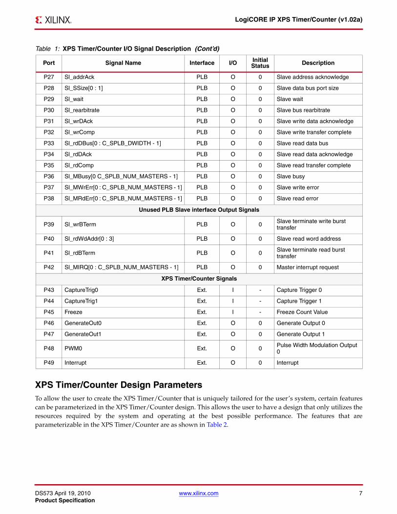
DS573 April 19, 2010 www.xilinx.com 7Product Specification
LogiCORE IP XPS Timer/Counter (v1.02a)
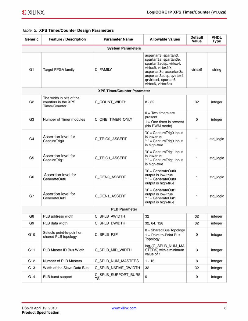
XPS Timer/Counter Design ParametersTo allow the user to create the XPS Timer/Counter that is uniquely tailored for the user’s system, certain featurescan be parameterized in the XPS Timer/Counter design. This allows the user to have a design that only utilizes theresources required by the system and operating at the best possible performance. The features that areparameterizable in the XPS Timer/Counter are as shown in Table 2.
P27 Sl_addrAck PLB O 0 Slave address acknowledge
P28 Sl_SSize[0 : 1] PLB O 0 Slave data bus port size
P29 Sl_wait PLB O 0 Slave wait
P30 Sl_rearbitrate PLB O 0 Slave bus rearbitrate
P31 Sl_wrDAck PLB O 0 Slave write data acknowledge
P32 Sl_wrComp PLB O 0 Slave write transfer complete
P33 Sl_rdDBus[0 : C_SPLB_DWIDTH - 1] PLB O 0 Slave read data bus
P34 Sl_rdDAck PLB O 0 Slave read data acknowledge
P35 Sl_rdComp PLB O 0 Slave read transfer complete
P36 Sl_MBusy[0 C_SPLB_NUM_MASTERS - 1] PLB O 0 Slave busy
P37 Sl_MWrErr[0 : C_SPLB_NUM_MASTERS - 1] PLB O 0 Slave write error
P38 Sl_MRdErr[0 : C_SPLB_NUM_MASTERS - 1] PLB O 0 Slave read error
Unused PLB Slave interface Output Signals
P39 Sl_wrBTerm PLB O 0 Slave terminate write burst transfer
P40 Sl_rdWdAddr[0 : 3] PLB O 0 Slave read word address
P41 Sl_rdBTerm PLB O 0 Slave terminate read burst transfer
P42 Sl_MIRQ[0 : C_SPLB_NUM_MASTERS - 1] PLB O 0 Master interrupt request
XPS Timer/Counter Signals
P43 CaptureTrig0 Ext. I - Capture Trigger 0
P44 CaptureTrig1 Ext. I - Capture Trigger 1
P45 Freeze Ext. I - Freeze Count Value
P46 GenerateOut0 Ext. O 0 Generate Output 0
P47 GenerateOut1 Ext. O 0 Generate Output 1
P48 PWM0 Ext. O 0 Pulse Width Modulation Output 0
P49 Interrupt Ext. O 0 Interrupt
Table 1: XPS Timer/Counter I/O Signal Description (Cont’d)
Port Signal Name Interface I/O Initial Status Description
DS573 April 19, 2010 www.xilinx.com 8Product Specification
LogiCORE IP XPS Timer/Counter (v1.02a)
Table 2: XPS Timer/Counter Design Parameters
Generic Feature / Description Parameter Name Allowable Values Default Value
VHDL Type
System Parameters
G1 Target FPGA family C_FAMILY
aspartan3, spartan3, spartan3a, spartan3e, spartan3adsp, virtex4, virtex5, virtex5fx, aspartan3e, aspartan3a, aspartan3adsp, qvirtex4, qrvirtex4, spartan6, virtex6, virtex6cx
virtex5 string
XPS Timer/Counter Parameter
G2The width in bits of the counters in the XPS Timer/Counter
C_COUNT_WIDTH 8 - 32 32 integer
G3 Number of Timer modules C_ONE_TIMER_ONLY
0 = Two timers are present1 = One timer is present (No PWM mode)
0 integer
G4 Assertion level for CaptureTrig0 C_TRIG0_ASSERT
’0’ = CaptureTrig0 input is low-true’1’ = CaptureTrig0 input is high-true
1 std_logic
G5 Assertion level for CaptureTrig1 C_TRIG1_ASSERT
’0’ = CaptureTrig1 input is low-true’1’ = CaptureTrig1 input is high-true
1 std_logic
G6 Assertion level for GenerateOut0 C_GEN0_ASSERT
’0’ = GenerateOut0 output is low-true’1’ = GenerateOut0 output is high-true
1 std_logic
G7 Assertion level for GenerateOut1 C_GEN1_ASSERT
’0’ = GenerateOut1 output is low-true’1’ = GenerateOut1 output is high-true
1 std_logic
PLB Parameter
G8 PLB address width C_SPLB_AWIDTH 32 32 integer
G9 PLB data width C_SPLB_DWIDTH 32, 64, 128 32 integer
G10 Selects point-to-point or shared PLB topology C_SPLB_P2P
0 = Shared Bus Topology1 = Point-to-Point Bus Topology
0 integer
G11 PLB Master ID Bus Width C_SPLB_MID_WIDTHlog2(C_SPLB_NUM_MASTERS) with a minimum value of 1
3 integer
G12 Number of PLB Masters C_SPLB_NUM_MASTERS 1 - 16 8 integer
G13 Width of the Slave Data Bus C_SPLB_NATIVE_DWIDTH 32 32 integer
G14 PLB burst support C_SPLB_SUPPORT_BURSTS 0 0 integer
DS573 April 19, 2010 www.xilinx.com 9Product Specification
LogiCORE IP XPS Timer/Counter (v1.02a)
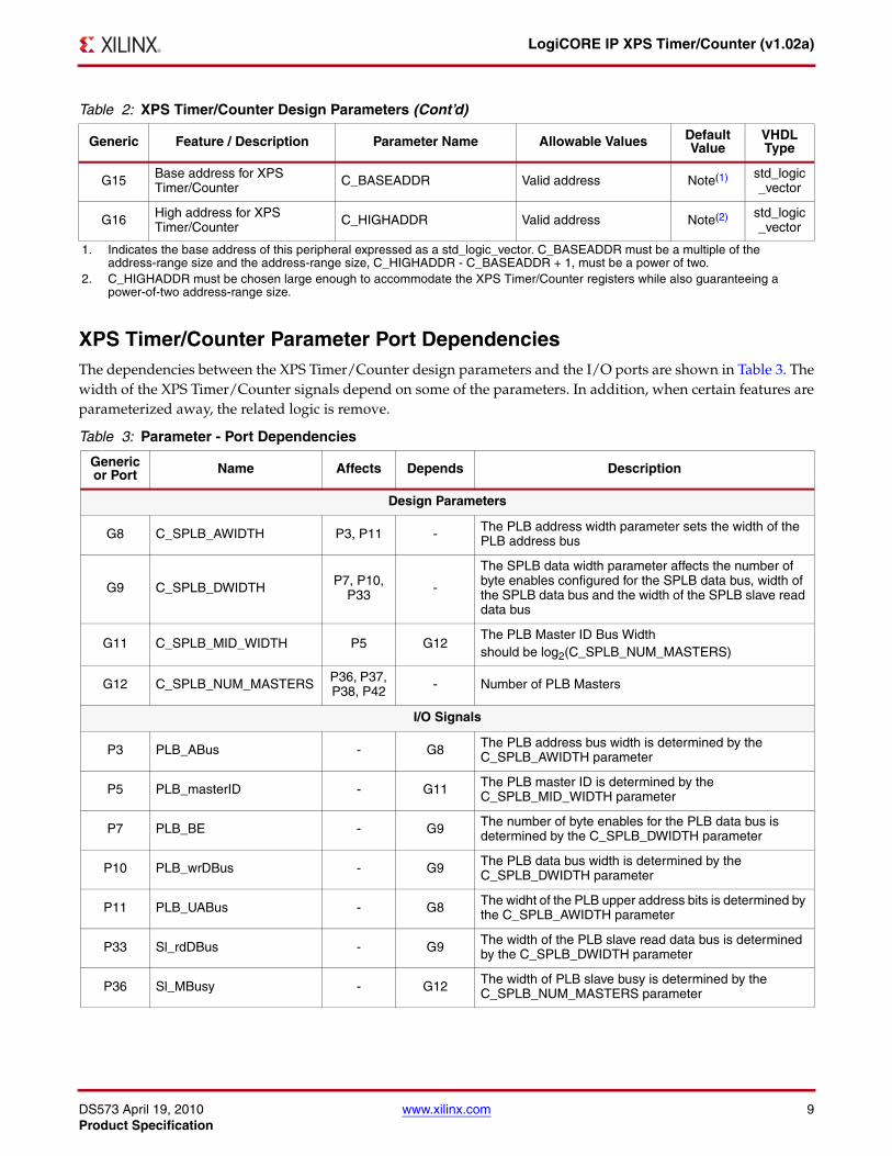
XPS Timer/Counter Parameter Port DependenciesThe dependencies between the XPS Timer/Counter design parameters and the I/O ports are shown in Table 3. Thewidth of the XPS Timer/Counter signals depend on some of the parameters. In addition, when certain features areparameterized away, the related logic is remove.
G15 Base address for XPS Timer/Counter C_BASEADDR Valid address Note(1) std_logic
_vector
G16 High address for XPS Timer/Counter C_HIGHADDR Valid address Note(2) std_logic
_vector
1. Indicates the base address of this peripheral expressed as a std_logic_vector. C_BASEADDR must be a multiple of the address-range size and the address-range size, C_HIGHADDR - C_BASEADDR + 1, must be a power of two.
2. C_HIGHADDR must be chosen large enough to accommodate the XPS Timer/Counter registers while also guaranteeing a power-of-two address-range size.
Table 3: Parameter - Port Dependencies
Generic or Port Name Affects Depends Description
Design Parameters
G8 C_SPLB_AWIDTH P3, P11 - The PLB address width parameter sets the width of the PLB address bus
G9 C_SPLB_DWIDTH P7, P10, P33 -
The SPLB data width parameter affects the number of byte enables configured for the SPLB data bus, width of the SPLB data bus and the width of the SPLB slave read data bus
G11 C_SPLB_MID_WIDTH P5 G12The PLB Master ID Bus Widthshould be log2(C_SPLB_NUM_MASTERS)
G12 C_SPLB_NUM_MASTERS P36, P37, P38, P42 - Number of PLB Masters
I/O Signals
P3 PLB_ABus - G8 The PLB address bus width is determined by the C_SPLB_AWIDTH parameter
P5 PLB_masterID - G11 The PLB master ID is determined by the C_SPLB_MID_WIDTH parameter
P7 PLB_BE - G9 The number of byte enables for the PLB data bus is determined by the C_SPLB_DWIDTH parameter
P10 PLB_wrDBus - G9 The PLB data bus width is determined by the C_SPLB_DWIDTH parameter
P11 PLB_UABus - G8 The widht of the PLB upper address bits is determined by the C_SPLB_AWIDTH parameter
P33 Sl_rdDBus - G9 The width of the PLB slave read data bus is determined by the C_SPLB_DWIDTH parameter
P36 Sl_MBusy - G12 The width of PLB slave busy is determined by the C_SPLB_NUM_MASTERS parameter
Table 2: XPS Timer/Counter Design Parameters (Cont’d)
Generic Feature / Description Parameter Name Allowable Values Default Value
VHDL Type

DS573 April 19, 2010 www.xilinx.com 10Product Specification
LogiCORE IP XPS Timer/Counter (v1.02a)
Register Data Types and Organization
Timer Counter registers are accessed as one of the following types:
• Byte (8 bits)
• Half word (2 bytes)
• Word (4 bytes)
The XPS Timer/Counter registers are organized as big-endian data. The bit and byte labeling for the big-endiandata types is shown in the Figure 3.
P37 Sl_MWrErr - G12 The width of PLB slave write error is determined by the C_SPLB_NUM_MASTERS parameter
P38 Sl_MRdErr - G12 The width of PLB slave read error is determined by the C_SPLB_NUM_MASTERS parameter
P42 Sl_MIRQ - G12 The width of Master interrupt request is determined by the C_SPLB_NUM_MASTERS parameter
X-Ref Target - Figure 3
Figure 3: Big-Endian Data Types
Table 3: Parameter - Port Dependencies (Cont’d)
Generic or Port Name Affects Depends Description
MS Byte
LS Byte
LS Byte
MS Bit
0 1 2 3
n n+2 n+3 n+1 Byte address
Byte label
Byte significance
Bit label
Bit significance
0 31
MS Byte
LS Bit
LS Byte
MS Bit
0 1
n n+1 Byte address
Byte label
Byte significance
Bit label
Bit significance
0 15
Word
Halfword
Byte
MS Byte
LS Bit MS Bit
0
n Byte address
Byte label
Byte significance
Bit label
Bit significance
0 7
DS573_03_041910
DS573 April 19, 2010 www.xilinx.com 11Product Specification
LogiCORE IP XPS Timer/Counter (v1.02a)
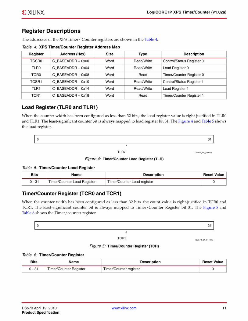
Register DescriptionsThe addresses of the XPS Timer/ Counter registers are shown in the Table 4.
Load Register (TLR0 and TLR1)
When the counter width has been configured as less than 32 bits, the load register value is right-justified in TLR0and TLR1. The least-significant counter bit is always mapped to load register bit 31. The Figure 4 and Table 5 showsthe load register.
Timer/Counter Register (TCR0 and TCR1)
When the counter width has been configured as less than 32 bits, the count value is right-justified in TCR0 andTCR1. The least-significant counter bit is always mapped to Timer/Counter Register bit 31. The Figure 5 andTable 6 shows the Timer/counter register.
Table 4: XPS Timer/Counter Register Address Map
Register Address (Hex) Size Type Description
TCSR0 C_BASEADDR + 0x00 Word Read/Write Control/Status Register 0
TLR0 C_BASEADDR + 0x04 Word Read/Write Load Register 0
TCR0 C_BASEADDR + 0x08 Word Read Timer/Counter Register 0
TCSR1 C_BASEADDR + 0x10 Word Read/Write Control/Status Register 1
TLR1 C_BASEADDR + 0x14 Word Read/Write Load Register 1
TCR1 C_BASEADDR + 0x18 Word Read Timer/Counter Register 1
X-Ref Target - Figure 4
Figure 4: Timer/Counter Load Register (TLR)
Table 5: Timer/Counter Load Register
Bits Name Description Reset Value
0 - 31 Timer/Counter Load Register Timer/Counter Load register 0
X-Ref Target - Figure 5
Figure 5: Timer/Counter Register (TCR)
Table 6: Timer/Counter Register
Bits Name Description Reset Value
0 - 31 Timer/Counter Register Timer/Counter register 0
0 31
TLRx DS573_04_041910
0 31
TCRxDS573_04_041910
DS573 April 19, 2010 www.xilinx.com 12Product Specification
LogiCORE IP XPS Timer/Counter (v1.02a)
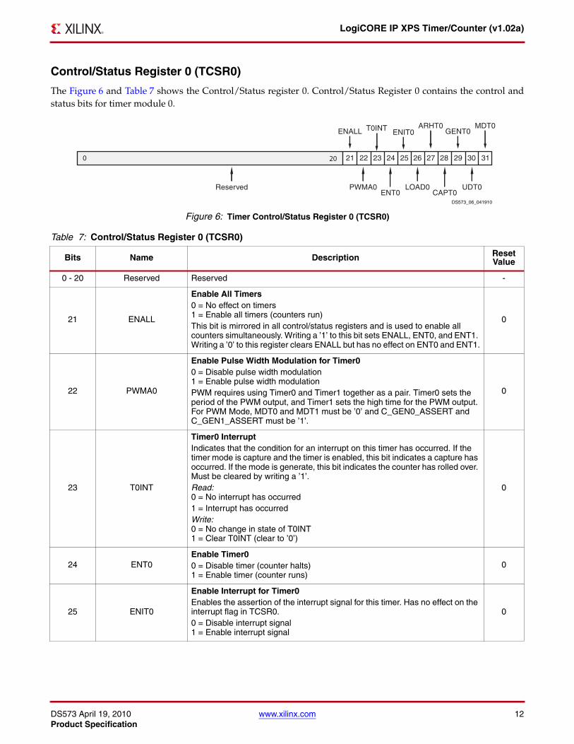
Control/Status Register 0 (TCSR0)
The Figure 6 and Table 7 shows the Control/Status register 0. Control/Status Register 0 contains the control andstatus bits for timer module 0.X-Ref Target - Figure 6
Figure 6: Timer Control/Status Register 0 (TCSR0)
Table 7: Control/Status Register 0 (TCSR0)
Bits Name Description Reset Value
0 - 20 Reserved Reserved -
21 ENALL
Enable All Timers0 = No effect on timers1 = Enable all timers (counters run)This bit is mirrored in all control/status registers and is used to enable all counters simultaneously. Writing a ’1’ to this bit sets ENALL, ENT0, and ENT1. Writing a ’0’ to this register clears ENALL but has no effect on ENT0 and ENT1.
0
22 PWMA0
Enable Pulse Width Modulation for Timer00 = Disable pulse width modulation1 = Enable pulse width modulationPWM requires using Timer0 and Timer1 together as a pair. Timer0 sets the period of the PWM output, and Timer1 sets the high time for the PWM output. For PWM Mode, MDT0 and MDT1 must be ’0’ and C_GEN0_ASSERT and C_GEN1_ASSERT must be ’1’.
0
23 T0INT
Timer0 InterruptIndicates that the condition for an interrupt on this timer has occurred. If the timer mode is capture and the timer is enabled, this bit indicates a capture has occurred. If the mode is generate, this bit indicates the counter has rolled over. Must be cleared by writing a ’1’.Read:0 = No interrupt has occurred1 = Interrupt has occurredWrite:0 = No change in state of T0INT1 = Clear T0INT (clear to ’0’)
0
24 ENT0Enable Timer00 = Disable timer (counter halts)1 = Enable timer (counter runs)
0
25 ENIT0
Enable Interrupt for Timer0Enables the assertion of the interrupt signal for this timer. Has no effect on the interrupt flag in TCSR0.0 = Disable interrupt signal1 = Enable interrupt signal
0
21 22 23 24 25 27 28 29 30 26 31
ENT0 LOAD0
CAPT0 UDT0 PWMA0
ENIT0 ARHT0 MDT0
GENT0 ENALL
Reserved
0 20
T0INT
DS573_06_041910
DS573 April 19, 2010 www.xilinx.com 13Product Specification
LogiCORE IP XPS Timer/Counter (v1.02a)
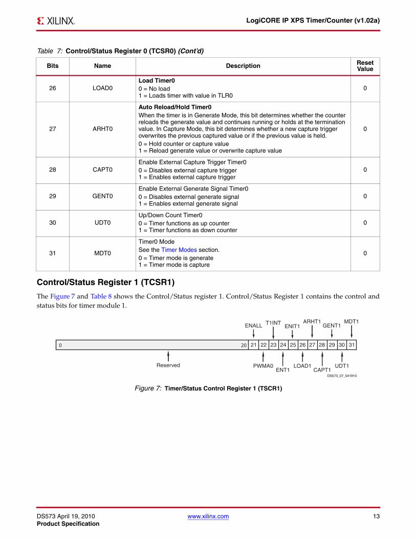
Control/Status Register 1 (TCSR1)
The Figure 7 and Table 8 shows the Control/Status register 1. Control/Status Register 1 contains the control andstatus bits for timer module 1.
26 LOAD0Load Timer00 = No load1 = Loads timer with value in TLR0
0
27 ARHT0
Auto Reload/Hold Timer0When the timer is in Generate Mode, this bit determines whether the counter reloads the generate value and continues running or holds at the termination value. In Capture Mode, this bit determines whether a new capture trigger overwrites the previous captured value or if the previous value is held.0 = Hold counter or capture value1 = Reload generate value or overwrite capture value
0
28 CAPT0Enable External Capture Trigger Timer00 = Disables external capture trigger1 = Enables external capture trigger
0
29 GENT0Enable External Generate Signal Timer00 = Disables external generate signal1 = Enables external generate signal
0
30 UDT0Up/Down Count Timer00 = Timer functions as up counter1 = Timer functions as down counter
0
31 MDT0
Timer0 ModeSee the Timer Modes section.0 = Timer mode is generate1 = Timer mode is capture
0
X-Ref Target - Figure 7
Figure 7: Timer/Status Control Register 1 (TSCR1)
Table 7: Control/Status Register 0 (TCSR0) (Cont’d)
Bits Name Description Reset Value
21 22 23 24 25 27 28 29 30 26 31
ENT1 LOAD1
CAPT1 UDT1 PWMA0
ENIT1 ARHT1 MDT1
GENT1 ENALL
Reserved
0 20
T1INT
DS573_07_041910
DS573 April 19, 2010 www.xilinx.com 14Product Specification
LogiCORE IP XPS Timer/Counter (v1.02a)
Table 8: Control/Status Register 1 (TCSR1)
Bits Name Description Reset Value
0 - 20 Reserved Reserved -
21 ENALL
Enable All Timers0 = No effect on timers1 = Enable all timers (counters run)This bit is mirrored in all control/status registers and is used to enable all counters simultaneously. Writing a ’1’ to this bit sets ENALL, ENT0, and ENT1. Writing a ’0’ to this register clears ENALL but has no effect on ENT0 and ENT1.
0
22 PWMB0
Enable Pulse Width Modulation for Timer10 = Disable pulse width modulation1 = Enable pulse width modulationPWM requires using Timer0 and Timer1 together as a pair. Timer0 sets the period of the PWM output, and Timer1 sets the high time for the PWM output. For PWM Mode, MDT0 and MDT1 must be ’0’ and C_GEN0_ASSERT and C_GEN1_ASSERT must be ’1’.
0
23 T1INT
Timer1 InterruptIndicates that the condition for an interrupt on this timer has occurred. If the timer mode is capture and the timer is enabled, this bit indicates a capture has occurred. If the mode is generate, this bit indicates the counter has rolled over. Must be cleared by writing a ’1’.Read:0 = No interrupt has occurred1 = Interrupt has occurredWrite:0 = No change in state of T1INT1 = Clear T1INT (clear to ’0’)
0
24 ENT1Enable Timer10 = Disable timer (counter halts)1 = Enable timer (counter runs)
0
25 ENIT1
Enable Interrupt for Timer1Enables the assertion of the interrupt signal for this timer. Has no effect on the interrupt flag in TCSR1.0 = Disable interrupt signal1 = Enable interrupt signal
0
26 LOAD1Load Timer10 = No load1 = Loads timer with value in TLR1
0
27 ARHT1
Auto Reload/Hold Timer1When the timer is in generate mode, this bit determines whether the counter reloads the generate value and continues running or holds at the termination value. In capture mode, this bit determines whether a new capture trigger overwrites the previous captured value or if the previous value is held until it is read.0 = Hold counter or capture value1 = Reload generate value or overwrite capture value
0
28 CAPT1Enable External Capture Trigger Timer10 = Disables external capture trigger1 = Enables external capture trigger
0
DS573 April 19, 2010 www.xilinx.com 15Product Specification
LogiCORE IP XPS Timer/Counter (v1.02a)
Implementation
Target Technology
The target technology is an FPGA listed in the Supported Device Family field of the LogiCORE Facts table.
Device Utilization and Performance Benchmarks
Core Performance
Because the XPS Timer/Counter core will be used with other design modules in the FPGA, the utilization andtiming numbers reported in this section are estimates only. System-level results will vary.
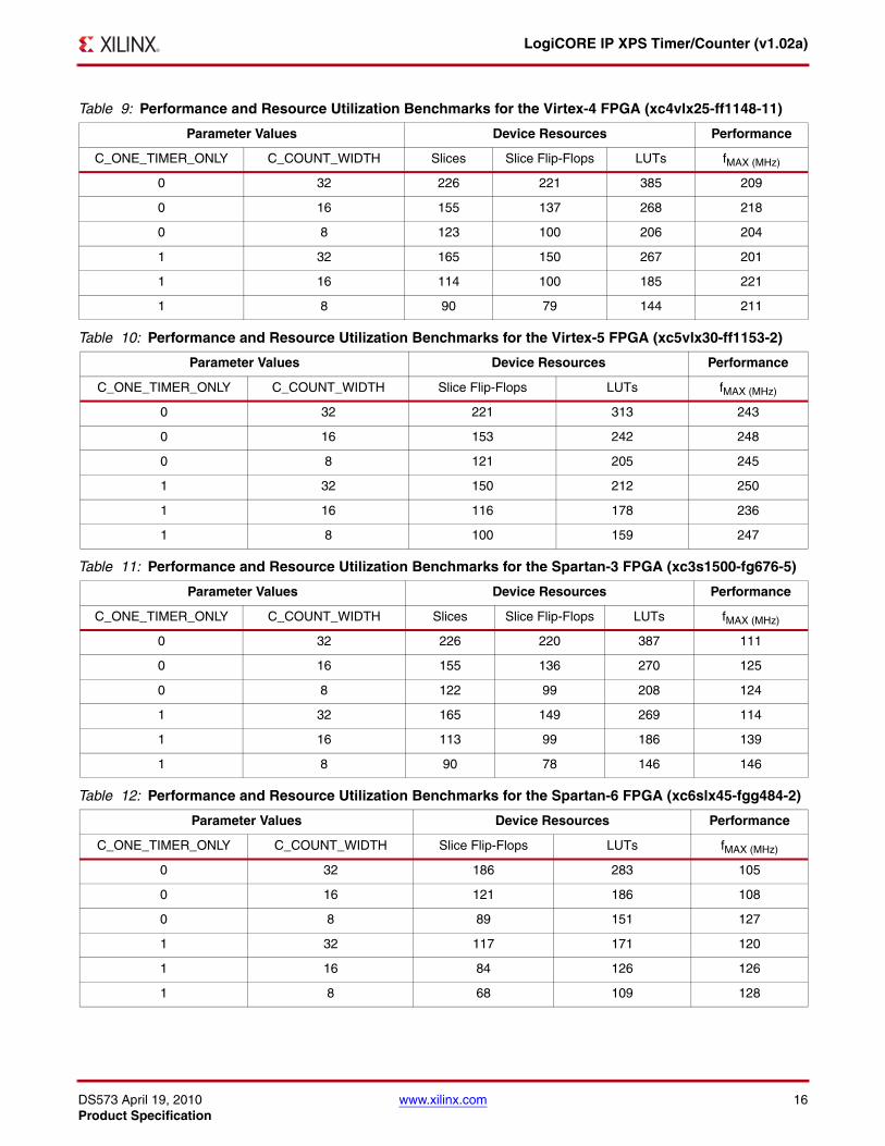
The XPS Timer/Counter resource utilization for various parameter combinations measured with the Virtex-4 FPGAas the target device is detailed in Table 9.
The XPS Timer/Counter resource utilization for various parameter combinations measured with the Virtex-5 FPGAas the target device is detailed in Table 10.
The XPS Timer/Counter resource utilization for various parameter combinations measured with the Spartan-3FPGA as the target device is detailed in Table 11.
The XPS Timer/Counter resource utilization for various parameter combinations measured with the Spartan-6FPGA as the target device is detailed in Table 12.
The XPS Timer/Counter resource utilization for various parameter combinations measured with the Virtex-6 FPGAas the target device is detailed in Table 13.
29 GENT1Enable External Generate Signal Timer10 = Disables external generate signal1 = Enables external generate signal
0
30 UDT1Up/Down Count Timer10 = Timer functions as up counter1 = Timer functions as down counter
0
31 MDT1
Timer1 ModeSee the Timer Modes section.0 = Timer mode is generate1 = Timer mode is capture
0
Table 8: Control/Status Register 1 (TCSR1) (Cont’d)
Bits Name Description Reset Value
DS573 April 19, 2010 www.xilinx.com 16Product Specification
LogiCORE IP XPS Timer/Counter (v1.02a)
Table 9: Performance and Resource Utilization Benchmarks for the Virtex-4 FPGA (xc4vlx25-ff1148-11)
Parameter Values Device Resources Performance
C_ONE_TIMER_ONLY C_COUNT_WIDTH Slices Slice Flip-Flops LUTs fMAX (MHz)
0 32 226 221 385 209
0 16 155 137 268 218
0 8 123 100 206 204
1 32 165 150 267 201
1 16 114 100 185 221
1 8 90 79 144 211
Table 10: Performance and Resource Utilization Benchmarks for the Virtex-5 FPGA (xc5vlx30-ff1153-2)
Parameter Values Device Resources Performance
C_ONE_TIMER_ONLY C_COUNT_WIDTH Slice Flip-Flops LUTs fMAX (MHz)
0 32 221 313 243
0 16 153 242 248
0 8 121 205 245
1 32 150 212 250
1 16 116 178 236
1 8 100 159 247
Table 11: Performance and Resource Utilization Benchmarks for the Spartan-3 FPGA (xc3s1500-fg676-5)
Parameter Values Device Resources Performance
C_ONE_TIMER_ONLY C_COUNT_WIDTH Slices Slice Flip-Flops LUTs fMAX (MHz)
0 32 226 220 387 111
0 16 155 136 270 125
0 8 122 99 208 124
1 32 165 149 269 114
1 16 113 99 186 139
1 8 90 78 146 146
Table 12: Performance and Resource Utilization Benchmarks for the Spartan-6 FPGA (xc6slx45-fgg484-2)
Parameter Values Device Resources Performance
C_ONE_TIMER_ONLY C_COUNT_WIDTH Slice Flip-Flops LUTs fMAX (MHz)
0 32 186 283 105
0 16 121 186 108
0 8 89 151 127
1 32 117 171 120
1 16 84 126 126
1 8 68 109 128
DS573 April 19, 2010 www.xilinx.com 17Product Specification
LogiCORE IP XPS Timer/Counter (v1.02a)
System Performance
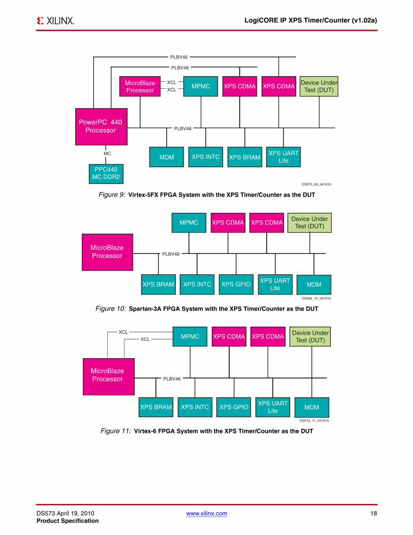
To measure the system performance (FMAX) of this core, this core was added to a Virtex-4 FPGA system, a Virtex-5system FPGA, Spartan-3A FPGA system, Virtex-6 FPGA system and a Spartan-6 FPGA system as the Device UnderTest (DUT) as shown in Figure 8, Figure 9, Figure 10, Figure 11 and Figure 12.
Because the XPS Timer/Counter core will be used with other design modules in the FPGA, the utilization andtiming numbers reported in this section are estimates only. When this core is combined with other designs in thesystem, the utilization of FPGA resources and timing of the core design will vary from the results reported here.
Table 13: Performance and Resource Utilization Benchmarks for the Virtex-6 FPGA (xc6vlx195t-ff11562-1)
Parameter Values Device Resources Performance
C_ONE_TIMER_ONLY C_COUNT_WIDTH Slice Flip-Flops LUTs fMAX (MHz)
0 32 186 365 203
0 16 121 232 202
0 8 89 174 203
1 32 117 217 202
1 16 84 149 201
1 8 68 124 209
X-Ref Target - Figure 8
Figure 8: Virtex-4 FX FPGA System with the XPS Timer/Counter as the DUT
PowerPC 405 Processor
MPMC XPS CDMADevice Under
Test (DUT)
XPS UARTLite
XPS GPIOXPS INTCXPS BRAM
DPLB1IPLB1
DPLB0
IPLB0
XPS CDMAPLBV46
PLBV46
PLBV46
DS582_08_041910
DS573 April 19, 2010 www.xilinx.com 18Product Specification
LogiCORE IP XPS Timer/Counter (v1.02a)
X-Ref Target - Figure 9
Figure 9: Virtex-5FX FPGA System with the XPS Timer/Counter as the DUT
X-Ref Target - Figure 10
Figure 10: Spartan-3A FPGA System with the XPS Timer/Counter as the DUT
X-Ref Target - Figure 11
Figure 11: Virtex-6 FPGA System with the XPS Timer/Counter as the DUT
MPMC XPS CDMADevice Under
Test (DUT)
XPS UARTLite
XPS INTC
XPS CDMA
MDM
XCL
XCL
PLBV46
MicroBlaze
XPS BRAMMDM
PPC440MC DDR2
MC
PLBV46
PLBV46
PowerPC 440Processor
MicroBlazeProcessor
DS573_09_041910
MicroBlazeProcessor
MPMC XPS CDMA
XPS UARTLite
XPS GPIOXPS INTCXPS BRAM
XPS CDMA
MDM
PLBV46
DS582_10_041910
Device UnderTest (DUT)
MicroBlazeProcessor
MPMC XPS CDMA
XPS UARTLite
XPS GPIOXPS INTCXPS BRAM
DS573_11_041910
XPS CDMA
MDM
XCL
XCL
PLBV46
Device UnderTest (DUT)
DS573 April 19, 2010 www.xilinx.com 19Product Specification
LogiCORE IP XPS Timer/Counter (v1.02a)
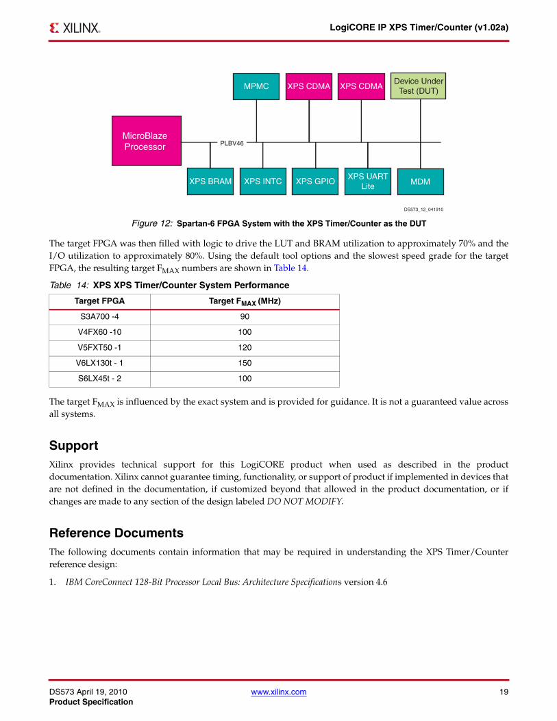
The target FPGA was then filled with logic to drive the LUT and BRAM utilization to approximately 70% and theI/O utilization to approximately 80%. Using the default tool options and the slowest speed grade for the targetFPGA, the resulting target FMAX numbers are shown in Table 14.
The target FMAX is influenced by the exact system and is provided for guidance. It is not a guaranteed value acrossall systems.
Support Xilinx provides technical support for this LogiCORE product when used as described in the productdocumentation. Xilinx cannot guarantee timing, functionality, or support of product if implemented in devices thatare not defined in the documentation, if customized beyond that allowed in the product documentation, or ifchanges are made to any section of the design labeled DO NOT MODIFY.
Reference DocumentsThe following documents contain information that may be required in understanding the XPS Timer/Counterreference design:
1. IBM CoreConnect 128-Bit Processor Local Bus: Architecture Specifications version 4.6
X-Ref Target - Figure 12
Figure 12: Spartan-6 FPGA System with the XPS Timer/Counter as the DUT
Table 14: XPS XPS Timer/Counter System Performance
Target FPGA Target FMAX (MHz)
S3A700 -4 90
V4FX60 -10 100
V5FXT50 -1 120
V6LX130t - 1 150
S6LX45t - 2 100
MicroBlazeProcessor
MPMC XPS CDMA
XPS UARTLite
XPS GPIOXPS INTCXPS BRAM
DS573_12_041910
XPS CDMA
MDM
PLBV46
Device UnderTest (DUT)
DS573 April 19, 2010 www.xilinx.com 20Product Specification
LogiCORE IP XPS Timer/Counter (v1.02a)
Ordering InformationThis Xilinx LogiCORE IP module is provided at no additional cost with the Xilinx ISE Design Suite EmbeddedEdition software under the terms of the Xilinx End User License. The core is generated using the Xilinx ISEEmbedded Edition software (EDK).
For more information, please visit the XPS Timer product web page.
Information about this and other Xilinx LogiCORE IP modules is available at the Xilinx Intellectual Property page.For information on pricing and availability of other Xilinx LogiCORE modules and software, please contact yourlocal Xilinx sales representative.
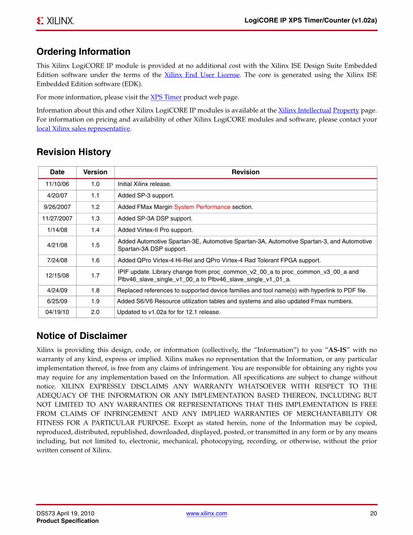
Revision History
Notice of DisclaimerXilinx is providing this design, code, or information (collectively, the “Information”) to you “AS-IS” with nowarranty of any kind, express or implied. Xilinx makes no representation that the Information, or any particularimplementation thereof, is free from any claims of infringement. You are responsible for obtaining any rights youmay require for any implementation based on the Information. All specifications are subject to change withoutnotice. XILINX EXPRESSLY DISCLAIMS ANY WARRANTY WHATSOEVER WITH RESPECT TO THEADEQUACY OF THE INFORMATION OR ANY IMPLEMENTATION BASED THEREON, INCLUDING BUTNOT LIMITED TO ANY WARRANTIES OR REPRESENTATIONS THAT THIS IMPLEMENTATION IS FREEFROM CLAIMS OF INFRINGEMENT AND ANY IMPLIED WARRANTIES OF MERCHANTABILITY ORFITNESS FOR A PARTICULAR PURPOSE. Except as stated herein, none of the Information may be copied,reproduced, distributed, republished, downloaded, displayed, posted, or transmitted in any form or by any meansincluding, but not limited to, electronic, mechanical, photocopying, recording, or otherwise, without the priorwritten consent of Xilinx.
Date Version Revision
11/10/06 1.0 Initial Xilinx release.
4/20/07 1.1 Added SP-3 support.
9/26/2007 1.2 Added FMax Margin System Performance section.
11/27/2007 1.3 Added SP-3A DSP support.
1/14/08 1.4 Added Virtex-II Pro support.
4/21/08 1.5Added Automotive Spartan-3E, Automotive Spartan-3A, Automotive Spartan-3, and Automotive Spartan-3A DSP support.
7/24/08 1.6 Added QPro Virtex-4 Hi-Rel and QPro Virtex-4 Rad Tolerant FPGA support.
12/15/08 1.7IPIF update. Library change from proc_common_v2_00_a to proc_common_v3_00_a and Plbv46_slave_single_v1_00_a to Plbv46_slave_single_v1_01_a.
4/24/09 1.8 Replaced references to supported device families and tool name(s) with hyperlink to PDF file.
6/25/09 1.9 Added S6/V6 Resource utilization tables and systems and also updated Fmax numbers.
04/19/10 2.0 Updated to v1.02a for for 12.1 release.
Top Related