Zeta® For Printed Circuit Boards - 4pcb.com · Zeta® is a new family of PCB materials. Zeta®...
33
Zeta® For Printed Circuit Boards
Transcript of Zeta® For Printed Circuit Boards - 4pcb.com · Zeta® is a new family of PCB materials. Zeta®...

1
Zeta® For Printed CircuitBoards

Technical Support for the family of businesses
- Technical Services- Research & Development- Field Installations- Process Development- Process Audits- Defect Analysis

Zeta® is a new family of PCB materials.
Zeta® materials are based on high performance polymers in FILM form.
Zeta® materials do not contain fiberglass.
Zeta® materials are provided as C stage or B stage films combined with copper foil.
Zeta® provides PCB fabricators an alternative to RCC and liquid dielectrics.
3

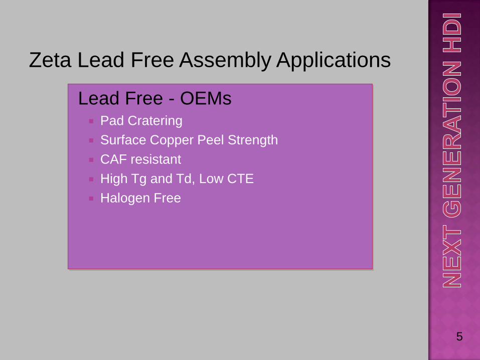
Lead Free - OEMs Pad Cratering Surface Copper Peel Strength CAF resistant High Tg and Td, Low CTE Halogen Free
HDI – PCB shops+ OEMs Thickness reduction Low Dk and Df Via Formation Plating Multiple Lam Cycles (>10)
4
Zeta Applications
Lead Free - OEMs Pad Cratering Surface Copper Peel Strength CAF resistant High Tg and Td, Low CTE Halogen Free
5
Zeta Lead Free Assembly Applications

PAD “CRATERING” Mechanically induced fracture in the resin between copper foil and
outermost layer of fiberglass. May be within the resin or at the resin to glass interface.
Pad remains connected to the component (usually BGA) and leaves a“Crater” in the PCB.
6

PAD “CRATERING” = Opens Fractures start in the dielectric (resin) and works through the copper trace creating an open circuit.
7

ZETA® Cap for Pad Cratering“Drop in” to existing designs Unique material properties,
Zeta® acts as a crack stop. Pad Crater solution without
changing base materials. Reduces need for under-fill. Resistant to field handling,
installation and service issues. Improves Drop test
performance. Hand held devices
Greater component rework success.
8
Zeta® Cap

9
0
10
20
30
40
50
60
70
80
0
500
1000
1500
2000
2500
3000
3500
4000
4500
Kapton Zeta Cap epoxy polyimide
Modulus kpsi (strength) % Elongation (flexibility)
Zeta CapIs more flexible than rigid, but 3 times stronger than flex. This prevents fractures from starting.

Copper ¼ oz (9 µm), 3/8 oz (12 µm), ½ oz (18 µm) Low tooth profile 6 to 7 pound peel strength RTF finish
C stage Dielectric 0.5 mil (12 µm), 1.0 mil (25 µm), 1.5 mil (38 µm) Non-copper side treated for prepreg bonding Tg > 300⁰C, Td > 500⁰C @ 2GHz – Dk = 3.0, Df = .005 Dielectric Strength – 4900 v/mil Halogen Free
10

UL 94-V0, MOT 155⁰C
Pad Crater Testing 1.0 mil with Pad Crater TV, hot pin pull test with OEM #1 Prototype boards built with 0.5 and 1.0 mil with OEM #1 Pad Crater TV PCBs under construction for OEM #2 Pad Crater TV design completed for OEM #3, PCB
construction to follow.
11

Questions regarding Zeta® lead free assembly applications?
12

HDI – PCB shops+ OEMs Thickness reduction Low Dk and Df Via Formation Plating Multiple Lam Cycles (>10)
13
Zeta HDI Applications

ZETA® C STAGE/ B STAGE PRODUCTS Zeta® Cap
Copper clad high Tg, low CTE fully cured dielectric.
Used with standard prepregs or Zeta® Bond.
Zeta® Bond Hi Tg “B” stage film that is glass free. Thickness is easily tailored to fill
areas around plated circuits. Hi peels, even after multiple lam
cycles.
Zeta® Lam Zeta® Cap + Zeta® Bond Ready to use in Lay-up without Prepreg
14

New epoxy technology for multiple lam cycles Non-dicy Non-phenolic
Room temp storageHigh Tg and High TdHigh flow and fill Low moisture absorbing Tg after 72 hours in boiling water- 174⁰C Moisture uptake @ 72 hours in boiling water – 1.0% Moisture uptake for Kapton, 24 hrs room temp -2.8%
Requires change in press cycle Start temp is 350⁰F instead of 200 - 250⁰F
15

Epoxy based high density crosslinking resin Requires more heat to gel Much longer shelf life - > 1 year Does not require refrigeration Non-brittle B stage Halogen free and not brittle after cure
350⁰F to gel in 15 minutes 375 ⁰F for 90 minutes to cure
16

ZETA® LAM Zeta® LAM
C-stage layer provides a polymer solution for glass fabric; Consistent thickness control after lamination Very high dielectric strength Lower Z-axis CTE than other glass free dielectrics materials Lower Dk, Lower loss High copper peels at high temperatures
B-stage layer provides; Bonding and fill of circuits and vias
Various thicknesses of resins are available for fill requirements
Curable with standard PCB laminating equipment (375ºF) Long shelf life, 1 year at room temperature
IPC-4563 Example –
Zeta Lam C25EP/B38E TSL AA =1/3 oz copper + 1.0 mil “C” stage polyimide +1.5 mils of “B” stage epoxy
17
Copper
B-Stage Epoxy
C-Stage Polyimide

ZETA® LAM Zeta® LAM
Available Coppers ¼ oz (9 micron) 3/8 oz (12 micron) ½ oz (18 micron)
C-stage layer ½ mil (12 micron) 1 mil (25 micron) 1.5 mil (38 micron)
B-stage layer 1 mil (25 micron) 1.5 mil (38 micron) 2.0 mil (50 micron)
18
Copper
B-Stage Epoxy
C-Stage Polyimide
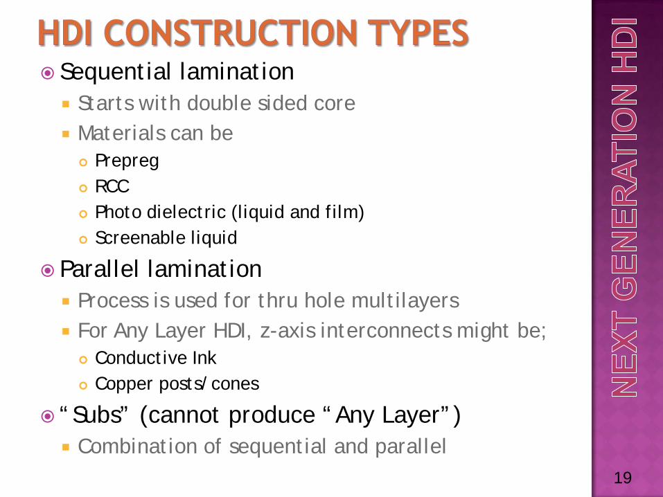
Sequential lamination Starts with double sided core Materials can be Prepreg RCC Photo dielectric (liquid and film) Screenable liquid
Parallel lamination Process is used for thru hole multilayers For Any Layer HDI, z-axis interconnects might be; Conductive Ink Copper posts/cones
“Subs” (cannot produce “Any Layer”) Combination of sequential and parallel
19

Sequential lamination Advantages “Any Layer” HDI capable Uses standard PCB processing Thin structures possible
Disadvantages Requires multiple laminations
Parallel lamination Advantages High layer count possible with one lamination cycle
Disadvantages Z-axis interconnect must be formed prior to lamination May require special process/equipment/materials Very thin layers (< 2 mil/50µ) hard to handle
Zeta can be used in both applications! 20

Finer copper traces are great for HDI But harder to produce with high yield As thickness gets reduced, so does Impedance To maintain the same Impedance; Line width must be reduced, or… Dk is reduced, this has the same effect. Zeta produces the same Impedance at half the
thickness with the same line width.
Thinner structures at the same Impedance have; Easier to drill and plate vias Lower via inductance Lower thermal impedance.
21

Zeta® for stacked vias
22
Sequential lamination is a popular way to make HDI structures. This requires one lamination cycle for each layer.

23
Thermal stress coupon
0.008” core + 9 layers of Zeta® Lam on each side.
20 layers
Overall thickness0.035”

24

25
Zeta® Bond SE used to fill the via
Testing applications eliminating the via fill process steps
Zeta® Bond SE resin available in thicknesses to meet many designs in filling via’s
Glass free allows for more resin to flow into vias

First Zeta Lam boards built and shipped February 2009, East Coast PCB shop
Zeta Lam boards shipped in October 2009, West Coast PCB shop.
Zeta Lam boards shipped by another West Coast PCB shop in March of 2009.
Zeta Lam boards built and shipped from Bay Area PCB shop for ongoing design with “Any Layer HDI” using 9 lamination cycles.
26

Zeta Cap has 94-V0 rating
Zeta Cap has MOT of 155⁰C
Zeta Lam/Bond SE flame testing in process 94-V0 expected
Zeta Lam/Bond MOT should be 155⁰C
27

IPC-4563 Resin coated copper (RCC) Many items are AABUS (as agreed between user and supplier)
Cover C-stage/B-stage combinations Spec allows for many different product types This is the best fit for Zeta® Lam and ZRC
IPC-JPCA-4104 High Density Interconnect (HDI) and Micro Via materials
Covers dielectrics, foils and z-axis connections Includes many different types of materials Does not specify C-stage/B-stage combinations
28

ZETA MATERIALS HAVE EXCELLENT THERMAL
PROPERTIES FOR GLASS FREE FILMS
Material Tg Td Z-axis CTE CommentsZeta Cap >300⁰C >500⁰C 19 ppm/⁰C Glass free film
Zeta Bond SE
180⁰C 400⁰C 60 ppm/⁰C Glass free film
Zeta Lam SE N/A N/A 40 ppm/⁰C Glass free film
Dicy curedHi Tg epoxy
180⁰C 300⁰C 55 ppm/⁰C Glass re-enforced 0.020” core
PhenolicEpoxy
180⁰C 340⁰C 45 ppm/⁰C Glass re-enforced 0.020” core
Flex EpoxyBonding
Film
100⁰C 285⁰C >150 ppm/⁰C Glass free film
29

ZETA MATERIALS HAVE EXCELLENT ELECTRICAL
PROPERTIES FOR GLASS FREE FILMS
Material Dk(2 GHz)
Df Breakdown Voltage
Comments
Zeta Cap 3.0 0.005 4900 v/mil Glass free film
Zeta Bond SE
3.2 0.010 2500 v/mil Glass free film
Zeta Lam SE 3.2 0.010 4900 v/mil Glass free film
Dicy curedHi Tg epoxy
4.2 0.014 1000 v/mil Glass re-enforced 0.020” core
PhenolicEpoxy
4.0 0.021 1350 v/mil Glass re-enforced 0.020” core
Flex EpoxyBonding
Film
3.2 0.020 3840 v/mil Glass free film
30

* values sited from manufacturers data sheet** values from independent lab testing on “C” stage
Manufacturer Part Thermal Conductivity (W/mK)
Thermal Resistance (˚C cm2/W)
Berquist MP-06503 *1.3 0.58HT-04503 *2.2 0.32HT-07006 *2.2 0.71CML-11006 *1.1 1.35
Laird T-LAM SS 1KA04 *3 0.34T-LAM SS 1KA06 *3 0.52T-LAM SS 1KA08 *3 0.70T-LAM SS HTD04 *2.2 0.46T-LAM SS HTD06 *2.2 0.69
Integral Tech. Zeta Bond 1 mil **0.58 0.44Zeta Cap 1 mil **0.43 0.59
Isola 370HR 106 **0.44 1.35406 106 **0.28 2.12
Dupont FR 1 mil **0.36 0.71Kapton 1 mil **0.14 1.82LF 1 mil **0.22 1.16CooLam LX03517016 *0.8 0.25CooLam LX07022016 *0.8 0.29

Questions regarding Zeta® HDI applications?
32

ZETA® HAS TWO BROAD BASE APPLICATIONSPAD CRATER FIXHDI
AS OF NOW, PAD CRATERING HAS NO OTHER FIXWe are being told this by many OEM’sZETA® FOR HDI
MANY COMBINATIONS, APPLICATIONS POSSIBLEBE CREATIVE! SAMPLES ARE AVAILABLE!
33