
Yole Equipment Materials for 3DIC Wafer Level Packaging Sample October 2012
21
© 2012 Equipment & Materials for 3DIC and Wafer-Level-Packaging The second complete REPORT and exhaustive DATABASE analyzing in details the equipment and materials tool-box for packaging at the wafer scale November - 2012 SUSS Brewer Science DuPont SPTS PlanOptikt EVG
-
Upload
wirebonder -
Category
Documents
-
view
287 -
download
8
description
3D IC Market Report Sample
Transcript of Yole Equipment Materials for 3DIC Wafer Level Packaging Sample October 2012

© 2012
Equipment & Materials for 3DIC and Wafer-Level-Packaging
The second complete REPORT and exhaustive DATABASE analyzing in details
the equipment and materials tool-box for packaging at the wafer scale
November - 2012
SUSS Brewer Science DuPont SPTS PlanOptikt EVG

© 2012 • 2
Copyrights © Yole Développement SA. All rights reserved.
Table of Content
• Scope of the report & definitions ..……. 4 – Objectives, key features, glossary
• Executive Summary ….………………… 11
1) 3DIC & WLP Equipment & Materials
2011 – 2017 market forecasts ...………. 41 – Equipment market forecasts (in units and M$ revenues)
…………………………………………………....…… 48
o Breakdown details for Wafer Bonders / die bonders /
C2W Bonders / DRIE etching & other drilling tools /
CVD / PVD / ECD Plating / Exposure & Lithography /
Spray coating / Cleaning / Temporary Bonding & De-
Bonding / Grinding-Thinning-CMP / Wafer-molding /
Inspection & Metrology / Test tools
– Competitive landscape and market share of main
equipment suppliers detailed
– Materials market forecasts (in M$ revenues)
…………………………………………………......….. 86
o Breakdown details for Photoresist & coatings /
Adhesive tapes / pre-applied & wafer-level underfills /
Molding compounds / Plating & cleaning chemistries /
Slurries for CMP / Temporary bonding materials/ Gas
& precursors / sputtering targets
– Competitive landscape and market share of main
material suppliers detailed
2) 3DIC & WLP technologies process flows &
manufacturing trends analysis ……...... 110 – Focus on Flip-chip wafer bumping …………….. 112
o Introduction & background
o Typical manufacturing process flows
o Equipment & Materials suppliers involved
o Key process challenges and issues
– Focus on WL CSP packaging …………………... 118
– Focus on FO WLP packaging ………………...... 136
– Focus on 2.5D silicon interposers ................... 148
– Focus on 3D WLP …………………..…………….. 162
– Focus on 3DIC & TSV „Via Middle‟ …………….. 170
– Focus on “Via first” TSV
for WLP MEMS Oscillator with TSV……………..205
3) DATABASE in excel format …...……...… 275 – Detailed analysis of the activity of the 375+ key
equipment & material suppliers of the wafer-level-
packaging tool-box solutions (activity profiling & key contacts)
• Conclusions & Perspectives …...……... 281
• Appendix ………………….……....…….…. 286

© 2012 • 3
Copyrights © Yole Développement SA. All rights reserved.
Scope of this report coverage
Wafer-level-packaging Platforms
Wafer-Level Electrical Redistribution
Flip-chip & Wafer-Level Stacking / Integration
WL CSP ‘Fan-in’
FOWLP ‘Fan-Out’
Glass / Silicon
Flip-chip wafer bumping
on BGA
3D IC
& TSV
Embedded IC in PCB / laminate
Wafer-Level Interface / Encapsulation
3D WLP For MEMS & sensors
(also called 3D SiP sometimes)
2.5D
interposers
Complete Equipment & Materials Tool-Box covered in this report!
Dry film &
adhesive tapes
Photo resist
& coatings
Mold compound
& underfills
Indirect mat. (chemistries, cleaning,
CMP slurries…)
FE / BE / LCD / PCB related equipments
(litho & exposure, etch, deposition, plating, bonding, handling,
molding, thinning , dicing, test, metrology, etc…)
…)
Substrates (carriers, cap,
interposers…)
Gas /
precursors

© 2012 • 4
Copyrights © Yole Développement SA. All rights reserved.
0.0
5.0
10.0
15.0
20.0
25.0
30.0
35.0
40.0
2011 2012 2013 2014 2015 2016 2017
Vo
lum
e (i
n M
un
its
of
30
0m
m w
afer
eq
.)
Global Wafer-Level-Packaging demand (in Munits of 300mm wafer eq.)
Yole Developpement © October 2012
The emerging flavors of the “Mid-end”
3DIC
Flip-chip
2.5D interposers
3D WLP
WL CSP
FO WLP
3D SiP
• « Mid-end » infrastructure is growing and is the main leading driver and the fastest growing
semiconductor packaging technology with more than 18% CAGR in units over the next 6 years
to come
– Wafer-level-packaging technologies are a huge business opportunity in the future: historically supported by the market
growth in flip-chip wafer bumping with electroplated gold, solder bumps and today copper pillars, wafer-level-packages are
actually coming in many different flavors, namely Fan-in WLCSP packages, 3D WLP, FO WLP packages, 2.5D Glass /
Silicon interposers and of course 3DIC integration with TSV interconnects.
– As this wafer-level-packaging industry develops over time, we are noticed that a real infrastructure has emerged by itself
into what is now being called the “Mid-end” of the semiconductor manufacturing environment. Indeed, wafer-level-
packages are true “Mid-end” technologies in the sense that they can all be served in the „blur zone‟ of overlap between the
IDMs or CMOS foundries' back-end-of-line (BEOL) wafer fabs and the back-end wafer bumping assembly facilities of the
OSATs and wafer bumping houses

© 2012 • 5
Copyrights © Yole Développement SA. All rights reserved.
Transforming IC Packaging Supply Chain*
System /
Product
Sub-Module /
Sub-systems Design & Assembly
Design of chip & package
Wafer Level
Packaging « Middle -end »
Silicon Manufacturing
« Front-end »
Package Assembly
& Final test « Back-end »
Front-end related
materials suppliers
OEMs (Original
Equipment
Makers)
FE related
equipment suppliers
BE Packaging
materials suppliers
BE Packaging
equipment suppliers
Fab-less
IC players
IDMs (Integrated Device Manufacturers)
Integrated wafer / package manufacturing foundries
OSATs (Open Source Assembly & Test houses)
WLP houses (no need for traditional substrate)
PWB suppliers (motherboard)
ODM / EMS / DMS
(electronic design &
manufacturing services)
Passive comp. & SMT materials
SMT equipment
suppliers
SiP design
houses
Package substrate
laminate suppliers
Substrate material suppliers (FR4, BT resin, Cu clad, etc…)
* Existing business models represented in red, new
business models in orange
Wafer
foundries
Fab-smart players (foundry services + focused internal investment in manufacturing & critical IP)
Wafer Bumping houses PCB / PWB houses with Embedded die capability

© 2012 • 6
Copyrights © Yole Développement SA. All rights reserved.
Detailed 3DIC & WLP Process Flow Analysis
• It‟s worth noting that there‟s a significant difference in how manufacturing is generally
performed in the front-end versus in the back-end worlds – The back-end has generally a much greater cost sensitivity but can face scaling issues with time when
semiconductor ICs continue to reduce in chip size while increasing in pin-count number
– On the other hand, front-end related technologies are more expensive initially but could be preferable
because of higher repeatability, yield, throughput and because of better perspectives in the long run when it
comes to be able to scale down the technology to smaller pitch dimension while maintaining cost pressure
• Yole‟s analysts have updated the previous
report “equipment & materials” based on the
different alternatives offered by the present
equipment and material tool-box for wafer-
level-packaging – All main scenarios are analyzed, including flip-chip
wafer bumping trends, Fan-in WLCSP, 3D WLP,
FOWLP, 2.5D silicon interposers, 3DIC Via Middle &
Via Last process scenarios

© 2012 • 7
Copyrights © Yole Développement SA. All rights reserved.
2011 2012 2013 2014 2015 2016 2017
Equipment market $869 M $646 M $867 M $1 208 M $1 725 M $2 579 M $3 773 M
Material market $596 M $714 M $890 M $1 190 M $1 503 M $1 962 M $2 186 M
$0 M
$500 M
$1 000 M
$1 500 M
$2 000 M
$2 500 M
$3 000 M
$3 500 M
$4 000 M
Sale
s fo
reca
sts
(M$
)
Global Equipment & Material market forecast for 3DIC & Wafer-Level-Packaging (in M$)
Equipment market
Material market
Yole Developpement © October 2012
• The wafer-level-packaging market remains a huge business opportunity and
shows the greatest potential for significant future growth in the semiconductor
industry.
– That can be explain by the 3D IC technology which is fundamentally changing how processing
is done and offers the opportunity for new equipment modifications and new materials
development
Market Forecasts For 3DIC / WLP equipment & materials
24%
28%

© 2012 • 8
Copyrights © Yole Développement SA. All rights reserved.
2011 Global equipment market for 3D TSV & WLP
Wafer
bonding
$52M
TB &
Debond
$43M
Spin coating/
Developer
~$100M
Spray
coating
~$15M
ECD Plating
$138M
DRIE
$30,5M CVD
~$12M PVD
~$81M
Inspection/
Metrology
~$72M
Lithography
~$134M
Others: ~$2M;
2% DNS
$8M
8%
SUSS
$30M
30%
TEL
$60M
60%
Ebara
~$35M
25%
Novellus/ LAM
Research : ~$7M; 5%
AMAT/
Semitool
$69M
50%
TEL/NEXX
~$28M
20%
LAM/ Novellu
s
$12M
39%
SPTS
$10M
33%
Others:
$3,1M;
10%
AMA
T
~$5M
18%
Rudolph
Technologi
es:~$32M
44%
Others:
~$6$; 9%
Nanometrics:
~$2M; 3%
FOGALE
~$3M; 4%
Camtek
~$26M
36%
KLA Tencor
$3M
4%
Othe
rs:
$0,6
M
TE
L/N
EX
X
~$
1M
; 1
0%
AM
AT
~$
5M
; 4
0%
SPTS
$8M;
10%
Others: ~$2M;
3%
Tango
Systems
$16M
23%
Oerlikon
$20M
28%
LAM Research/
Novellus: $0,5M
0,6%
AMAT
$24M
34%
TEL/ NEXX
$9,6M
12%
Others
~$2M;
3%
TEL
$6M
12%
SUSS
~$11
M
22%
EVG
$33M
63%
TAZM
O/ 3M
~$11M
25%
SUSS
~$11
M
25%
TEL
~$7M
5%
TOK
~$4M
15%
EVG
~$11
M
25%
SUSS
~$13
M
82%
DNS
$1M;
6%
EVG
~$2
M
12%
Ultratech
$57M
43%
ASML
~$23M
17%
SUSS
~$51M
38%
Others: ~$3M
SP
TS
~$
5M
; 1
5%
Grinding
~$27M
DISCO
~$17,6
M
65%
ACCRE
TECH
~$4,1M
15%
Okamot
o $2,7M
10%
Starsbaug
h
$1,4M; 5µ
Others: $1,4M;
5%
SA
MP
LE
TOTAL: ~$870M

© 2012 • 9
Copyrights © Yole Développement SA. All rights reserved.
2011 Global materials market for 3D TSV & WLP
Others
$14M
13%
JSR Micro
$4M; 4%
Sumito Bakelite/
Promerus
$7M; 7%
Fujifilm
$23M; 22%
HD Microsystems/
Dupont
$28M
26%
DOW Chemical
$26M
25%
AZ Electronis Materials
$3M; 3%
Others
$3,3M
30%
Nagase
$7,7M
70%
Others $5M; 5%
Indium
$7M
15%
Sekisui
Chemicals
$14M
30%
Nippon
Micrometal
$9M
20%
Mitsubishi
Materials
$14M
30%
OM Group Ultra
Pure Chemicals
$10M
20%
ATOTECH
$19M
40%
Enthone
(Cookson Elect)
$14M
30%
Others
$4,8M
10% Hitachi Chemi
$1M; 2%
Cabot Micro
$36M
75%
AGC
~$6M
12%
Air Products
~$5M
10%
Others; $0,5$
Honeywell
$5,0M; 8%
Zeon Chemicals
$16M
25%
Dynaloy
$16M
25%
AZ Electronis
Materials
$6; 10%
Others: $1,2M; 2%
OM Group Ultra
Pure Chemicals
$12M
20%
Shin-Etsu Chemical
$6M
10%
TOK
$26M
20%
AZ Electronis Materials
$39M
30%
JSR Micro
$52M
40%
Dupont $3M; 2%
Dow electronic materials
$3M; 2%
Shin-Etsu Chemical; $4M
3%
Shin-Etsu Micro Si
$4M; 3%
Permanent dielectric
resists
$106,2M
Wafer Molding
compound
$11M
Solder paste
$46M
Plating
chemistries
$48M
Slurries for CMP
$48M
Cleaning chemistries
$62M Strippable plating resists
$130M
TOTAL: ~$590M

© 2012 • 10
Copyrights © Yole Développement SA. All rights reserved.
TEL (Tokyo Electron LTD.)
$60.0 M 60%
SUSS Microtec $30.0 M
30%
Dai Nippon SCREEN $8.0 M
8%
Others* $2.3 M
2%
Spin coating & Developer equipment for 3D & WLP 2011 Market Share Breakdown by supplier (in M$)
Yole Developpement © October 2012
* SSEC, EVG, TAZMO, TOK, Toray engineering, Ushio
2011 Spin-Coater/ Developer Equipment Market
3D & WLP Market share per equipment supplier
• Total market related to the spin coater & developer equipment market is assessed at $100M in 2011.
• The key providers active in spin coating & developer equipment are:
– TEL, SUSS MicroTec and Dai Nippon Screen
TEL has strong leadership in the middle-end packaging market especially related to the coating + developer
track equipment set
SUSS Micro is a key leader in spinc oater dedicated to WLP applications
TOT ~ 100 M$
© 2012 • 11
Copyrights © Yole Développement SA. All rights reserved.
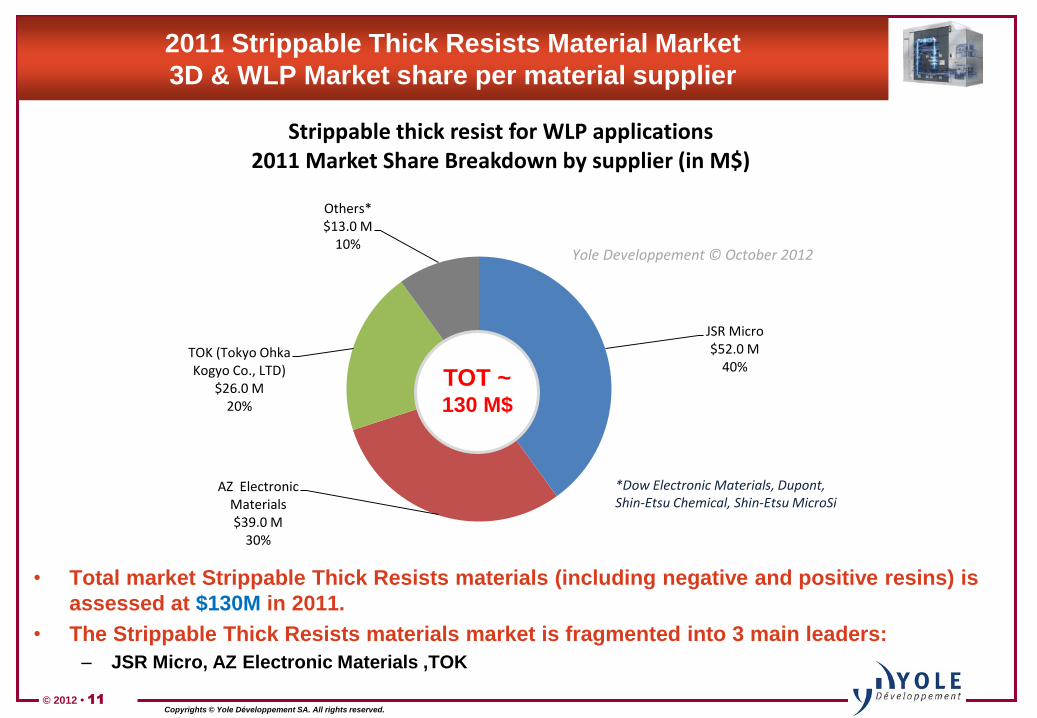
2011 Strippable Thick Resists Material Market
3D & WLP Market share per material supplier
• Total market Strippable Thick Resists materials (including negative and positive resins) is
assessed at $130M in 2011.
• The Strippable Thick Resists materials market is fragmented into 3 main leaders:
– JSR Micro, AZ Electronic Materials ,TOK
JSR Micro $52.0 M
40%
AZ Electronic Materials $39.0 M
30%
TOK (Tokyo Ohka Kogyo Co., LTD)
$26.0 M 20%
Others* $13.0 M
10%
Strippable thick resist for WLP applications 2011 Market Share Breakdown by supplier (in M$)
*Dow Electronic Materials, Dupont, Shin-Etsu Chemical, Shin-Etsu MicroSi
Yole Developpement © October 2012
TOT ~ 130 M$
© 2012 • 12
Copyrights © Yole Développement SA. All rights reserved.
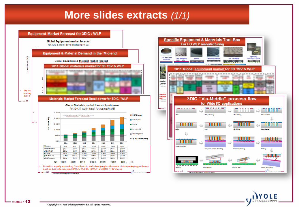
More slides extracts (1/1)

© 2012 • 13
Copyrights © Yole Développement SA. All rights reserved.
DATABASE with 375+ key Equipment & Material
Suppliers for 3DIC / WLP
• The database wad steadily updated with new key equipment & materials suppliers – Along with this new research and updated report, Yole is delivering an excel database screening and
profiling the detailed activity of more than 375+ small to medium to giant equipment & material suppliers
coming either from Front-end, Back-end assembly, PCB, LCD or Solar industries and providing actual
solutions for the 3DIC & wafer-level-packaging tool-box
• One of the main move this year was the acquisition of NEXX by TEL, Tokyo
Electron, in March 2012, enabling the company to expand and enhance their
position in advanced packaging by being involved in electrochemical deposition
(ECD) and physical vapor deposition (PVD) systems.

© 2012 • 14
Copyrights © Yole Développement SA. All rights reserved.
375+ companies cited in this Report / Database
3M, 3MTS, 4Pico, Ablestik, ACCRETECH, ADEKA CORPORATION, Adtec Engineering, Advanced Chemical Company , Advanced Inquiry Systems,
Advantest, AGC, AI TEchnology Inc, Aimsolder, AIR LIQUIDE, Air Products, AJI – dvanced Jisso Technology, Ajinomoto Fine Techno Co Inc., Akrion
systems, AkroMetrix LLC, Alchimer, ALSI, Altatech Semiconductor, AMEC, Amicra Microtechnologies GmbH, AML, Anji Microelectronics, Applied
Materials, Applied Relay Testing, Applied Spectra, Asahi Kasei E-Materials Corporation, ASM Pacific Technologies, ASML Netherlands B.V.,
Assembleon, AST (Samurai), ASYS GmbH, ATI, ATMI, ATOTECH, Auros Tech, Austin American Technology Corp, Axcelis Technologies, Ayumi
Industry Co. Ltd., AZ Electronic Materials, Azores Corp, Barth Electronics, BASF, Bergquist Company, Berliner Glass, Blue-M, Boschman
Technologies B.V., Brewer Science, Bruker AXS , Cabot electronics, CAMTEK USA, Canon ANELVA, Cascade Microtech, CHAPMAN, Chomerics,
Corning, Corning Incorporated, CSM Instruments, Cyantek, Cyber-Technologies, Daxin Materials Corporation, Datacon Technology GmbH (BESI),
DCG Systems, DEK semiconductor, DELO, Delta Design, Denka, Disco Corporation, DJ DevCorp, Dai Nippon SCREEN, Dongjin Semichem Co.,
Doublecheck Semiconductors, Dow Corning Corporation, Dow Electronic Materials, DRY PLASMA SYSTEMS, D-Tek Technology Co.,Ltd, DuPont
Electronic Technologies, Dynaloy, DYNATEX International, Eastman Chemical, EBARA Technologies Corp., Ebina Denka, ECI Technology, EEJA,
Electroglas Inc, ENF Technology Co .Ltd, Enterprix, Enthone (Cookson Electronics), Epoxy Technology Inc., ERS – gmbh, ESEC AG, ESI, Etched in
Time Inc, EV Group, Evest Corp., EXCICO, Exelsius, FASSE CO., LTD., Fico molding (BESI), Finetech, FOGALE Nanotech, Frontier Semiconductor, Frt
Of America, FSI International, Fuji Polymers, FUJIFILM Electronic Materials, Furukawa America GE Sensing & Inspection, Gore, GPD Global, Inc.,
Hamamatsu, HamaTech APE GmbH & Co. KG, HD MicroSystems, Henkel Corporation, Heraeus GmbH, Hesse & Knipps, Hitachi Chemical Co., Ltd.,
Hitachi High Technologies Corporation, Honeywell Electronic Materials, HORIBA Semiconductor, Hoya, IceMOS Technology, ICOS Vision Systems
NV, Ikonix Imaging, Indium Corporation, Ishihara Chemical , Ismeca Europe Semiconductor SA, JENOPTIK, Jet Metal, JSR Micro, Kester, KiyoKawa
Plating industry, KLA-TENCOR, Koh Young Technology Inc., Kulicke & Soffa, Kyzen Corporation, Laird Technologies, LAM Research Corporation ,
Laserod, Lasertec Corporation, Lauffer Presses, Leybold Optics USA Inc, LG Chem., Ltd., Life Bioscience, LincoTec, Linde Gas, Lintec, Loadpoint,
LORD Corporation, Mapper Lithography, Materion, Mattson Technology, Mechatronic Systemtechnik, MECO, MEMC Electronic Materials, Inc. ,
Metryx, MicroChem, MicroFab Technologies Inc, Micronic Laser Systems AB, Micronics Japan Co., Mitshubishi Gas Chemical, Mitsubishi Chemical
Corporation, Mitsubishi Electric, Mitsubishi Heavy Industry (MHI), Mitsubishi Materials, Mitsubishi Materials Corporation, Mitsui Chemicals,
Momentive performance material, MSG Lithoglas AG, MTK Co, Ltd., Mühlbauer, Nagase & Co., Ltd., Namics, Nanda Tech GmbH, NANOPLAS,
Nanovea, NEC / SCHOTT, Newport, NEXX Systems, Nikko Metal, Nikon Corporation, Nippon Electric Glass – NEG, Nippon Kayaku Co., Ltd., Nippon
Sheet Glass – NSG, Nissan Chemical Industries, Nitta Haas Inc., Nitto Denko Corporation, Norcom Systems Inc, Nordson ASYMTEK, Inc., Nordson
dage, Nordson March, NOVELLUS, nScrypt Inc., Nusil Silicone Technology, Nypro Inc., oak-mitsui technologies, OEM group, Oerlikon, Okmetic,
Olympus-ITA, Inc., OM Group Ultra Pure Chemicals Pte. Ltd., OPµS, Orbotech Ltd., Oxford Instrument, Pac Tech, Palomar Technologies Inc.,
Panasonic Denko, PANASONIC Factory Solutions, Philips Applied Technologies, picoDRILL, Plan Optik AG GmbH, Polymatech, Potomac Laser,
Praxair.com, Promerus LLC, Protavic America, Inc., PVA TePla AG, Ramgraber GmbH, rasco, REC Silicon, RENA GmbH, Replisaurus Technologies,
Ricmar Technology GmbH, Rorze, Rudolph Technologies, Saint-Gobain, SAMCO Inc. , Schmoll Machinen, Schott AG, SCS - Speciality Coating
Systems, Sekisui Chemical Co., Ltd., Semiconductor Technologies & Instruments (ASTI), Semprius, Senju Metal Industry Co., Ltd., SENTECH
Instruments, SET - Smart Equipment Technology, Seto Engineering Co., Ltd., Shanghai Micro Electronics Equipment , Shanghai Sinyang, Shibaura
Mechatronics Corporation, Shibuya Kogyo, Shin-Etsu Chemical Co.,Ltd. , Shin-Etsu MicroSi, Inc, SHINKAWA LTD., Shinko Seiki, Silecs, Singulus,
SOITEC, Sokudo Co. Ltd., SolMateS, Solvay, SolVision, SONIX, SONOSCAN, SPP (Sumitomo Precision Products Co., Ltd.), SPTS, SSEC - Solid State
Equipment Corporation, Starfire Systems Inc., STIL SA, Strasbaugh, Sumco Corporation, Sumitomo Bakelite, Sumitomo Chemicals, Surface Science
Integartion, SUSS Microtec, Sysmelec, Takada, Takatori Ltd., Tamar Technology, Tamarack Scientific, Tango Systems, tecnisco, TEGAL, TEL (Tokyo
Electron LTD.), Teradyne, Thin materials AG, Timbre Technologies, tok, TOK (Tokyo Ohka Kogyo Co., LTD), Toray engineering Co.Ltd, Toray
Industries, Inc, TOWA Corporation, TRESKY, TRIOPTICS, Ultraspray, Ultratech , ULVAC Inc., Umicore, Uyemura Co.Ltd, Uyemura International
Corporation, Veeco, Verigy, Viscom AG, West-Bond, Inc., Xradia, YAMADA CORPORATION, Young Chang Chemical, YoungTek Electronics Corp.,
Zebra Optical, Zeon Chemicals L.P., Zetta Core, Zygo Corporation, Zymet, Inc.

© 2012 • 15
Copyrights © Yole Développement SA. All rights reserved.
About the authors of this report
Jerome Baron Jerome is leading the MEMS &
Advanced Packaging market
research at Yole Developpement.
He has been following the 3D
packaging market evolution
since its early beginnings at
device, equipment and material
levels. He was granted a Master
of Science degree in
Nanotechnologies from the
National Institute of Applied
Sciences in Lyon, France
Contact: [email protected]
Amandine Pizzagalli Amandine recently joined Yole
Development Advanced Packaging
and MEMS manufacturing teams
after graduating as an engineer in
Electronics, with a specialization in
Semiconductors and Nano
Electronics Technologies. She
worked in the past for Air Liquide
with an emphasis on CVD and ALD
processes for semiconductor
applications
Contact: [email protected]

© 2012 • 16
Copyrights © Yole Développement SA. All rights reserved.
Who should be interested in this report?
• Equipment & Material suppliers – Assess the TAM – total accessible market of
your company‟s related products in the
wafer-level-packaging areas
– Identify technology trends, challenges and
precise requirements for each 3DIC / WLP
scenarios
– Screen competition activity, identify possible
partnerships or targets for M&As in areas
close to your current business
• R&D organizations & Investors – Monitor the global activity and consolidation
currently happing in the semiconductor
equipment & material business in order to
identify new partners, targets and take the
right decision before committing to one
particular supplier
• IDMs, CMOS foundries & OSAT
players – Get an exhaustive list of the 350+
equipment & materials companies
supplying solutions in the different 3DIC
and wafer-level-packaging areas
– Understand technology trends and
benchmark several different 3DIC & WLP
scenarios including the future trends for
PANEL scale packaging based on LCD /
PCB infrastructures
• PCB substrate manufacturers – Get the complete list of semiconductor
packaging equipment & materials
companies supplying solutions in the
blooming 3DIC & wafer-level-packaging
area
– Identify technology trends, challenges
and issues for each 3D packaging
scenario

© 2012 • 17
Copyrights © Yole Développement SA. All rights reserved.
Yole Developpement Company Presentation

© 2012 • 18
Copyrights © Yole Développement SA. All rights reserved.
Yole activities in Advanced Packaging
Media business News feed / Magazines / Webcasts
www.yole.fr
© 2009
Copyrights © Yole Développement SARL. All rights reserved.
HB-LED Packaging Technology & Market Trends
IR
Osram
Market Research
Reports
Market research, Technology & Strategy
Consulting services

© 2012 • 19
Copyrights © Yole Développement SA. All rights reserved.
Our Global Presence & Activity
Yole Inc.
Yole Développement
Lyon (HQ).
Yole Europe
Yole Japan
30% of our activity is
in North America
30% of our activity is
in Asia
40% of our activity is in
EU Countries
Yole Taiwan
Yole Korea

© 2012 • 20
Copyrights © Yole Développement SA. All rights reserved.
Supporting the Entire Value Chain
Yole consultants provide Market Analysis, Technology Evaluation and Business Plan Assessment for clients along the entire value chain
Institutions Investors
& Advocates
Integrators &
End Users
Device &
Module Makers
Material &
Equipment Suppliers

© 2012 • 21
Copyrights © Yole Développement SA. All rights reserved.
Via First / Via Last? 3D integration Scenarios
I
M
E
C
S
i
l
e
x
F
r
e
e
s
c
a
l
e
N
o
k
i
a
D
u
P
o
n
t
TSV+ Cost Analysis Tool for
your 3D IC manufacturing
3D IC & TSV 2010 Market Analysis
I
M
E
C
S
i
l
e
x
F
r
e
e
s
c
a
l
e
N
o
k
i
a
D
u
P
o
n
t
$27
7% $23
6%
$109
26%
$82%$37
9%$92%
$317%
$168
41%
TSV Scenario Cost structure breakdown
Via / Etching Drilling
Via Isolation
Via filling
Temporary bonding
Thinning
Stress release
BEOL (Pads)
Bonding
IPD - Thin-film Integrated Passive Devices
WL CSP 2012 Report update
N
o
k
i
a
2.5D Glass & Silicon
interposers - 2010 Report
© 2010
Copyrights © Yole Développement SA. All rights reserved.
MEMS Packaging Market & Technology Trends
1995
Sidebraze DIP
1996-2002
Plastic PDIP
1999 - today
SMT SOIC
& Die Down
2006
Stacked Die
QFN
~125 sq mm ~100 sq mm ~25 sq mm
6 & 6 mm
1995
Sidebraze DIP
1996-2002
Plastic PDIP
1999 - today
SMT SOIC
& Die Down
2006
Stacked Die
QFN
~125 sq mm ~100 sq mm ~25 sq mm
6 & 6 mm
Our latest advanced packaging
market research reports
© 2010
Copyrights © Yole Développement SARL. All rights reserved.
Advanced PackagingEquipment & Materials
NEC-Schott
SUSS Brewer ScienceSTSEVG
DuPont
Equipment & Materials for 3DIC & Wafer-Level-Packaging
Flip-chip 2011 Report
FO WLP & Embedded die
Wafer Packaging Fabs
DATABASE
© 2009
Copyrights © Yole Développement SARL. All rights reserved.
HB-LED Packaging Technology & Market Trends
IR
Osram
LED Packaging Market & Technology Trends


![WP91 Lucia Montanaro Kosovo State Building Conundrum 3dic[1]](https://static.fdocuments.in/doc/165x107/577d27671a28ab4e1ea3d6e5/wp91-lucia-montanaro-kosovo-state-building-conundrum-3dic1.jpg)


![Yole 3DIC & TSV Interconnects July 2012 Sample[1]](https://static.fdocuments.in/doc/165x107/54650439af795974338b4c77/yole-3dic-tsv-interconnects-july-2012-sample1.jpg)