Xilinx Spartan -3A Evaluation Kit User Guide - Arizona State …kyle135/Supplementary/FPGA/SP… ·...
21
Xilinx ® Spartan ™ -3A Evaluation Kit User Guide Rev. 2.1
Transcript of Xilinx Spartan -3A Evaluation Kit User Guide - Arizona State …kyle135/Supplementary/FPGA/SP… ·...
Xilinx® Spartan™-3A Evaluation Kit
User Guide Rev. 2.1

2 of 21 Rev 2.0 11/20/2008
Released Literature # ADS-005204
Table of Contents
1.0 Introduction ...............................................................................................................................................................................3 1.1 Description............................................................................................................................................................................3 1.2 Features ...............................................................................................................................................................................3 1.3 Reference Designs ...............................................................................................................................................................5 1.4 Ordering Information.............................................................................................................................................................5
2.0 Functional Description ..............................................................................................................................................................5 2.1 Xilinx Spartan-3A FPGA .......................................................................................................................................................7 2.2 Cypress PSoC Mixed-Signal Array.......................................................................................................................................7 2.3 Memory.................................................................................................................................................................................8
2.3.1 Parallel Flash ...............................................................................................................................................................9 2.3.2 Serial SPI Flash .........................................................................................................................................................10
2.4 Interfaces............................................................................................................................................................................12 2.4.1 USB 2.0 .....................................................................................................................................................................12 2.4.2 USB-UART ................................................................................................................................................................12 2.4.3 Digilent Headers ........................................................................................................................................................12 2.4.4 Miscellaneous I/O ......................................................................................................................................................13 2.4.5 LEDs..........................................................................................................................................................................13 2.4.6 GPIO Header (2 x 20) ................................................................................................................................................13 2.4.7 I
2C Temperature Sensor ............................................................................................................................................14
2.5 Module Clocks ....................................................................................................................................................................14 3.0 Configuration...........................................................................................................................................................................15
3.1 Configuration Modes ..........................................................................................................................................................15 4.0 Module Power .........................................................................................................................................................................16 5.0 PCB Stackup...........................................................................................................................................................................19 6.0 Acknowledgements.................................................................................................................................................................20
Figures
Figure 1 - Spartan-3A Evaluation Board Picture.........................................................................................................................................4 Figure 2 - Spartan-3A Evaluation Board Block Diagram ............................................................................................................................6 Figure 3 - Spartan-3A Evaluation Board Memory Interfaces ......................................................................................................................8 Figure 4 - SPI Interfaces...........................................................................................................................................................................11 Figure 5 - Digilent Header Pinout .............................................................................................................................................................12 Figure 6 - Xilinx Parallel IV Connector......................................................................................................................................................15 Figure 7 - Configuration Jumper (JP4) .....................................................................................................................................................16 Figure 8 - Power Supply Sequencing .......................................................................................................................................................17 Figure 9 - +3.3 V Power Supply Startup ...................................................................................................................................................17 Figure 10 - +1.2 V Power Supply Startup .................................................................................................................................................18 Figure 11 - PCB Layer Stack....................................................................................................................................................................19
Tables Table 1 - Ordering Information ...................................................................................................................................................................5 Table 2 - XC3S400A FT256 I/O Allocation.................................................................................................................................................7 Table 3 - Parallel Flash Interface Pinout ....................................................................................................................................................9 Table 4 - FPGA SPI Interface Pinout........................................................................................................................................................10 Table 5 - SPI Header J8 Pinout................................................................................................................................................................10 Table 6 - USB-UART Signals ...................................................................................................................................................................12 Table 7 - Digilent Header Connections.....................................................................................................................................................13 Table 8 - PSoC/FPGA Push Buttons........................................................................................................................................................13 Table 9 - LED assignment ........................................................................................................................................................................13 Table 10 - GPIO Connector (J4) pin assignment......................................................................................................................................14 Table 11 - Module Clocks.........................................................................................................................................................................14 Table 12 - FPGA Configuration Mode Jumper (JP4) Settings..................................................................................................................15

3 of 21 Rev 2.0 11/20/2008
Released Literature # ADS-005204
1.0 Introduction The purpose of this manual is to describe the functionality and contents of the Spartan®-3A Evaluation Kit from Avnet. This document includes instructions for operating the board, descriptions of the hardware features and explanations of the example projects.
1.1 Description
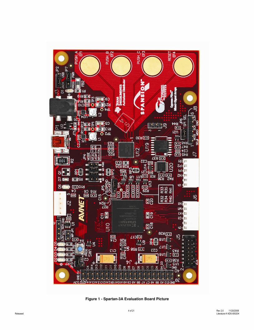
The Spartan-3A Evaluation Kit provides a platform for engineers designing with the Xilinx Spartan-3A FPGA and/or Cypress PSoC® Mixed Signal Array. The board provides the necessary hardware to not only evaluate the advanced features of these devices but also to implement user applications using peripherals and expansion connectors on the Spartan-3A evaluation board. Figure 1 is a picture if the Spartan-3A evaluation board; the block diagram in Figure 2 provides a high-level view of the components and interconnects.
1.2 Features
• Xilinx 3S400A-4FTG256C FPGA
• Clocks
16 MHz Oscillator (Maxim)
12 MHz Clock from PSoC device
32 kHz Clock from PSoC device • Memory
32 Mb Page-Mode Flash Memory (Spansion)
128 Mb SPI Flash Memory (Spansion)
• Interfaces
USB 2.0 (PSoC)
JTAG Programming/Configuration Port Temperature Sensor (Texas Instruments)
• Buttons and switches
Four User LEDs
Four PSoC CapSense capacitive switches
Four FPGA user “pushbuttons” (forwarded from PSoC CapSense switches)
Reset Push Button Switch • User I/O and expansion
Digilent 6-pin header (2)
2x20 0.1” Expansion Connector • Configuration and Debug
JTAG
4 of 21 Rev 2.0 11/20/2008
Released Literature # ADS-005204
Figure 1 - Spartan-3A Evaluation Board Picture

5 of 21 Rev 2.0 11/20/2008
Released Literature # ADS-005204
1.3 Reference Designs
Reference designs that demonstrate some of the potential applications of the Spartan-3A Evaluation Kit are available. See the PDF document included with each reference design for a complete description of the design and detailed instructions for running a demonstration on the development board.
1.4 Ordering Information
Table 1 lists the evaluation kit part number.
Part Number Hardware
AES-SP3A-EVAL400-G Xilinx Spartan-3A Evaluation Kit
Table 1 - Ordering Information
2.0 Functional Description A Xilinx Spartan-3A (XC3S400A-4FTG256C) 400 K gate FPGA and a Cypress Cy8C24894 PSoC Mixed-Signal Array are the primary components of the Avnet Spartan-3A evaluation board. In addition to on-board processing functions, the PSoC device provides off-board communication via a USB 2.0 full-speed interface. Communication between the PSoC and FPGA is facilitated by a 3.3 V level RS-232 interface between the two devices. This, along with several GPIO lines interconnecting the PSoC and FPGA, provide control and data-transfer mechanisms. A high-level block diagram of the Spartan-3A evaluation board is shown in Figure 1. As can be seen in Figure 1, the USB controller (PSoC), an SPI port, and an I
2C port provide off-board communication mechanisms. On-board memory
consists of a 128 Mbit SPI memory that may be used by either the PSoC or the FPGA, with FPGA access controlled by the PSoC; and 32 Mbit parallel Flash memory interfaced to the FPGA. Subsequent sections provide details of the board design.

6 of 21 Rev 2.0 11/20/2008
Released Literature # ADS-005204
Spartan-3A
XC3S400A
FT256
USB
Controller
(PsOC) UART
JTAG
USB
Conn
JTAG
Conn
SPI
Memory
128Mb
SPI
Port
I2C
Temp
Sensor
I2C
Port
Config
Mode
Jumpers
12MHz Clock32kHz Clock
16MHz
Oscillator
“Push”
Switches
(4)
Power
Supply
1.2V
3.3V
Power
Jack
5V
5V USB
Parallel Flash
Memory
4M x 8 / 2M x 16
User LEDs
(4)
Done LED
GPIOs (12)
2x20 Conn
35 User I/Os
3.3V, 5V, GND
Two 6-pin Headers
I/Os (4), 3.3V, GND
Figure 2 - Spartan-3A Evaluation Board Block Diagram

7 of 21 Rev 2.0 11/20/2008
Released Literature # ADS-005204
2.1 Xilinx Spartan-3A FPGA
The Xilinx XC3S400A-4FTG256C device designed onto the Spartan-3A evaluation board provides four I/O banks with Vccaux and I/O voltage of all banks fixed at +3.3 V. The ability to power Vcco and Vccaux from a common rail is a feature of the Spartan-3A that allows a lower-cost board design. Note that because Vccaux is set at +3.3 V, each design’s UCF must contain the statement:
CONFIG VCCAUX = “3.3”;
The four I/O banks are described in Table 2 and detailed I/O pin usage is provided throughout this document. Note that all pins utilized are bidirectional (regardless of usage), the XC3S400A input-only pins are not utilized in this implementation.
I/O Bank
# I/O
Function Number of I/O
pins
0 2 x 20 Expansion Connector (J4) 32
0 16 MHz Clock 1 (GCLK4)
0 LED 1
0 UART (FPGA-PSoC Communication) 2 0 Parallel Flash 1 0 FPGA Configuration 1
1 2 x 20 Expansion Connector (J4) 1 1 LED 3
1 I2C Interface 2
1 PSoC I/O 1
1 Parallel Flash 26 *
2 SPI Interface 6 *
2 Parallel Flash 16
2 12 MHz Clock 1 (GCLK0) 2 32 kHz Clock 1 (GCLK13)
2 LED (AWAKE) 1
2 FPGA Configuration (M[0:2]) 3 3 Digilent Headers J6, J7) 8
3 FPGA Reset (from PSoC) 1 3 “Pushbuttons” (CapSense via PSoC) 4
3 PSoC I/O 11 3 2 x 20 Expansion Connector (J4) 2
Table 2 - XC3S400A FT256 I/O Allocation
* Note that SPI Flash MISO and Parallel Flash D0 are a common FPGA connection
2.2 Cypress PSoC Mixed-Signal Array
The Cypress Cy8C24894 is a configurable device containing analog and digital blocks and peripheral devices that allow the user to create customized configurations to support different applications. As configured on the Spartan-3A evaluation board, the PSoC provides a full-speed (12 Mbps) USB interface, RS-232, SPI and I
2C interfaces, four capacitive touch-pads (the
condition of which is sent to the FPGA), and 15 general-purpose I/O lines (12 connected to the FPGA and three connected to header J9). A 6-pin header that is compatible with the Cypress Mini-Programmer allows configuration of the PSoC’s Flash program store. Additionally, the PSoC’s JTAG interface may be utilized to program the FPGA; e.g., the FPGA bit file transferred to the PSoC via USB and the PSoC JTAG interface transfers the file into the FPGA.

8 of 21 Rev 2.0 11/20/2008
Released Literature # ADS-005204
2.3 Memory
The Spartan-3A evaluation board is populated with both parallel Flash memory (4 Mbytes) and 128 Mbit SPI Serial to support various types of applications. Both Parallel Flash and SPI Serial Flash may be used for FPGA configuration. Figure 2 shows a high-level block diagram of the memory interfaces on this board
Figure 3 - Spartan-3A Evaluation Board Memory Interfaces

9 of 21 Rev 2.0 11/20/2008
Released Literature # ADS-005204
2.3.1 Parallel Flash
Parallel Flash memory consists of a single 32 Mbit Spansion S29GL032N in a TSOP-56 package interfaced to the FPGA. This device (U22) may be utilized in a 4 M x 8 or a 2 M x 16 configuration by control of the Flash_BYTE# signal. Flash_BYTE# is pulled low through a 10 K resistor to establish the 4 M x 8 default configuration that may be used for FPGA configuration. Following configuration, the FPGA may drive Flash_BYTE# high to establish the 2 M x 16 configuration. Jumper JP1 may be used to write-protect the Flash memory by placing a shunt across pins 1 and 2; default setting is JP1 open. Note the PCB layout also supports the same Spansion Flash device in a TSSOP-48 package. Table 3 provides the FPGA/FLASH pinout.
Parallel Flash Signal FPGA Pin# Parallel Flash Signal FPGA Pin#
Flash_CE# P15 Flash_D0 T14
Flash_OE# R15 Flash_D1 R13 Flash_WE# N13 Flash_D2 T13
Flash_RY/BY# A4 Flash_D3 P12 Flash_BYTE# N14 Flash_D4 N8
FLASH_RESET# T10 Flash_D5 P7
Flash_A0 P16 Flash_D6 T6 Flash_A1 N16 Flash_D7 T5
Flash_A2 L13 Flash_D8 P11 Flash_A3 K13 Flash_D9 R3
Flash_A4 M15 Flash_D10 N11
Flash_A5 M16 Flash_D11 N7 Flash_A6 L14 Flash_D12 R5
Flash_A7 L16 Flash_D13 T4 Flash_A8 J12 Flash_D14 P6
Flash_A9 J13 Flash_D15 N14 (Flash_A0) Flash_A10 G16 Flash_A11 F16
Flash_A12 H13 Flash_A13 G14
Flash_A14 E16 Flash_A15 F15
Flash_A16 G13
Flash_A17 F14
Flash_A18 E14
Flash_A19 F13 Flash_A20 D16 Flash_A21 D15
Table 3 - Parallel Flash Interface Pinout
10 of 21 Rev 2.0 11/20/2008
Released Literature # ADS-005204
2.3.2 Serial SPI Flash
128 Mbits of serial Flash memory is provided by a Spansion S25FL128P device (U19) interfaced to the Spartan-3A FPGA via its dedicated SPI interface, and to the Cypress PSoC device via a 2:1 multiplexer (U20). This multiplexer is controlled by the PSoC, which is master of this SPI interface. There are two SPI modes as depicted in Figure 3; PSoC/FPGA �� SPI Flash (PSoC_SPI_MODE=0) and PSoC �� FPGA (PSoC_SPI_MODE=1).
In the PSoC/FPGA �� SPI Flash mode, either the PSoC or the FPGA may access the SPI Flash by driving its select line low. This is done through an AND gate (U21) that will drive the SPI Flash’s chip select line (SF_SEL#) low in response to a low select signal from the FPGA (FPGA_SPI_SEL#) or the PSoC (PSoC_SPI_SEL). Note that the SPI clock line (SPI_CLK) may be driven by either the PSOC or the FPGA. Since this configuration has the potential for conflict, if the PSoC intends to access the SPI Flash, it must drive the FPGA’s PROG_B pin low to place the FPGA in a reset state to prevent it accessing the SPI Flash. The normal scenario for this would be that the PSoC would drive PROG_B low and download (via USB) an FPGA bit file that it would program into the SPI flash. When this is complete the PSoC would drive the FPGA’s mode pins to place it into SPI boot mode, release PROG_B, and the FPGA would access the SPI flash to load its bit file.
In the PSoC �� FPGA mode (PSoC_SPI_MODE=1) the multiplexer is configured to interconnect the PSoC and FPGA SPI interfaces; the purpose of this is to enable slave serial configuration from PSoC to FPGA. In this mode the PSoC is master and the FPGA will act as slave. Since the FPGA’s SPI interface is only active during SPI boot mode, implementation of the FPGA’s slave interface must be accomplished via firmware. While this configuration happens to share common pins with the FPGA SPI port, they will function as slave serial in this mode. Table 4 provides the FPGA’s SPI interface pinout.
6-pin header J8 may be used to allow the PSoC to expand the SPI interface to an external environment. Since the PSoC’s SPI select signal (PSoC_SPI_SEL#) is common to the SPI Flash as well as the SPI expansion interface, the default jumper on JP6 must be removed prior to using the SPI expansion. Table 5 provides the J8 pinout. Note that J8 pin 6 provides +3.3 V to another board; if that board is already powered then J8 pin 6 must not be connected.
Signal FPGA Pin#
FPGA_MOSI P10 FPGA_MISO T14
SPI_CLK R14 FPGA_SPI_SEL T2
Table 4 - FPGA SPI Interface Pinout
Signal J8 Pin#
PSoC_SPI_SEL# 1
SPI_FLASH_SI 2
SPI_FLASH_SO 3
SPI_CLK 4 GND 5 +3.3V 6
Table 5 - SPI Header J8 Pinout

11 of 21 Rev 2.0 11/20/2008
Released Literature # ADS-005204
Sp3A400
PsOC
SPI Flash
FPGA_MOSI
PsOC_MOSISPI_FLASH_SI
FPGA_MISO
PsOC_MISOSPI_FLASH_SO
Sp3A400
PsOC
SPI Flash
FPGA_MOSI
PsOC_MOSI
FPGA_MISO
PsOC_MISO
PsOC_SPI_MODE = 0
PsOC_SPI_MODE = 1
MUX
MUX
SPI_CLK
SP
I_C
LK
PsOC_SPI_SEL#
FPGA_SPI_SEL#
FPGA_SPI_SEL#
PsOC_SPI_SEL#
Figure 4 - SPI Interfaces
12 of 21 Rev 2.0 11/20/2008
Released Literature # ADS-005204
2.4 Interfaces
Interfaces on the Spartan-3A evaluation board consist of USB 2.0 via the PSoC, two 0.1” 6-pin right-angle headers designed to interface to Digilent
TM modules, a 0.1” 2 x 20 header providing connectivity to available FPGA general-purpose I/O pins, a 0.1”
1 x 6 header for SPI interface expansion, and a sensor providing temperature information via an I2C interface.
2.4.1 USB 2.0
USB Mini-AB connector P1 connects the PSoC device to a full-speed (12 Mbps) USB host. Power supplied by the USB host via connector P1 (+5V_USB) may be used to power the Spartan-3A evaluation board by jumpering JP2 1:2.
2.4.2 USB-UART
The USB-UART interface is used for communication between the PSoC and the FPGA but is not utilized externally (e.g., there is no RS-232 connector). This interface operates at 3.3 V and is the mechanism by which the FPGA communicates via USB; e.g., the PSoC device provides UART/USB translation. Note that the net names UART_RXD and UART_TXD on the schematic are named in terms of the PSoC connection. Net UART_RXD is an output from the FPGA and an input to the PSoC, as shown by the direction of the off-page connectors on the schematic. The FPGA Tx signal is connected to the PSoC Rx signal and then the PSoC re-broadcasts the data to the USB. For incoming data from USB, the PSoC transmits on the UART_TXD net which is actually an Rx for the FPGA.
Net Name Description FPGA Pin #
FPGA_RS232_Rx Received Data, RD (Transmitted by PsOC)
A3
FPGA_RS232_Tx Transmit Data, TD (Received by PsOC)
B3
Table 6 - USB-UART Signals
2.4.3 Digilent Headers
Two right-angle, 6-pin (1 x 6 female) Digilent headers (J6, J7) are interfaced to the FPGA, with each header providing 3.3 V power, ground, and four I/O’s. These headers may be utilized as general-purpose I/Os or may be used to interface to Digilent modules. J6 and J7 are placed in close proximity (0’9”-centers) on the PCB in order to support dual Digilent modules. Figure 4 shows the pinout of the Digilent headers; Table 7 provides the FPGA pinout. For Digilent modules see: http://www.digilentinc.com/Products/Catalog.cfm?Nav1=Products&Nav2=Peripheral&Cat=Peripheral Avnet offers a bundle of Digilent peripheral modules (part # HW-CRII-PM-ACC-G): http://em.avnet.com/part/xlx/c/HW-CRII
Figure 5 - Digilent Header Pinout

13 of 21 Rev 2.0 11/20/2008
Released Literature # ADS-005204
J6 Signal FPGA Pin#
DIGI2_0 N1
DIGI2_1 M1 DIGI2_2 K1
DIGI2_3 G1 J7 Signal FPGA Pin#
DIGI1_0 R1 DIGI1_1 P2
DIGI1_2 P1
DIGI1_3 N2
Table 7 - Digilent Header Connections
2.4.4 Miscellaneous I/O
Four user push button switches are provided via capacitive touch-pads connected to the Cypress PSoC device. A “touch” at any of these four pads is sensed by the PSoC and forwarded to the FPGA; these “push buttons” and their relationship to the FPGA are depicted in Table 8. Note that FPGA_RESET is a “soft” reset intended for FPGA code usage and does not perform any type of FPGA hardware reset.
PSoC Cap Sense FPGA “Pushbutton” FPGA Pin#
EF1 FPGA_PUSH_A K3
EF2 FPGA_PUSH_B H5
EF3 FPGA_PUSH_C L3 EF4 FPGA_RESET H4
Table 8 - PSoC/FPGA Push Buttons
2.4.5 LEDs
Four LEDs are provided for signaling purposes and connected to the FPGA as shown in Table 9. The corresponding FPGA pin must be driven high to light an LED.
LEDs FPGA Pin#
LED1 (D5) D14
LED2 (D4) C16
LED3 (D3) C15
LED4 (D2) B15
Table 9 - LED assignment
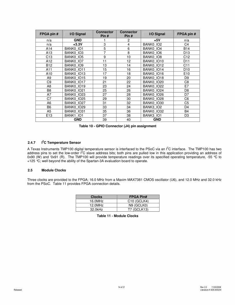
2.4.6 GPIO Header (2 x 20)
Some unused FPGA pins are connected to 0.1” 2 x 20-pin header J4. Signal names and connector pin/FPGA pin connections are identified in Table 10. All I/O’s are +3.3 V CMOS.
14 of 21 Rev 2.0 11/20/2008
Released Literature # ADS-005204
FPGA pin # I/O Signal Connector
Pin # Connector
Pin # I/O Signal FPGA pin #
n/a GND 1 2 +5V n/a n/a +3.3V 3 4 BANK0_IO2 C4
A14 BANK0_IO1 5 6 BANK0_IO4 B14 A13 BANK0_IO3 7 8 BANK0_IO6 D13 C13 BANK0_IO5 9 10 BANK0_IO8 C12
A12 BANK0_IO7 11 12 BANK0_IO10 D11 B12 BANK0_IO9 13 14 BANK0_IO12 C11
A11 BANK0_IO11 15 16 BANK0_IO14 D10
A10 BANK0_IO13 17 18 BANK0_IO16 E10 A9 BANK0_IO15 19 20 BANK0_IO18 D9
C9 BANK0_IO17 21 22 BANK0_IO20 C8 A8 BANK0_IO19 23 24 BANK0_IO22 E7
B8 BANK0_IO21 25 26 BANK0_IO24 D8 A7 BANK0_IO23 27 28 BANK0_IO26 D7 C7 BANK0_IO25 29 30 BANK0_IO28 C6
A6 BANK0_IO27 31 32 BANK0_IO30 C5 B6 BANK0_IO29 33 34 BANK3_IO2 D4
A5 BANK0_IO31 35 36 BANK0_IO32 B4 E13 BANK1_IO1 37 38 BANK3_IO1 D3
GND 39 40 GND
Table 10 - GPIO Connector (J4) pin assignment
2.4.7 I2C Temperature Sensor
A Texas Instruments TMP100 digital temperature sensor is interfaced to the PSoC via an I2C interface. The TMP100 has two
address pins to set the low-order I2C slave address bits; both pins are pulled low in this application providing an address of
0x90 (W) and ‘0x91 (R). The TMP100 will provide temperature readings over its specified operating temperature, -55 °C to +125 °C; well beyond the ability of the Spartan-3A evaluation board to operate.
2.5 Module Clocks
Three clocks are provided to the FPGA; 16.0 MHz from a Maxim MAX7381 CMOS oscillator (U6), and 12.0 MHz and 32.0 kHz from the PSoC. Table 11 provides FPGA connection details.
Clocks FPGA Pin#
16.0MHz C10 (GCLK4) 12.0MHz N9 (GCLK0)
32.0kHz T7 (GCLK13)
Table 11 - Module Clocks

15 of 21 Rev 2.0 11/20/2008
Released Literature # ADS-005204
3.0 Configuration
The Spartan-3A evaluation board provides four mechanisms to program and configure the FPGA; these are JTAG, Parallel Flash, Serial Flash, and the Cypress PSoC. The storage devices (Flash and SPI) cannot be programmed via the JTAG connector. The FPGA is the only thing in the JTAG chain on the Spartan-3A evaluation board; however, depending on the setting of configuration jumpers M[2:0], any of these can be the configuration source. The serial Flash, Parallel Flash, and PSoC are described earlier in this document. Programming the Spartan-3A evaluation board via Boundary Scan requires that a JTAG download cable be attached to the 14-pin 2 mm spaced header J5 (Figure 5) with a ribbon cable or with flying leads. If the Xilinx Parallel Cable IV is used, the ribbon cable connector mates with the keyed J5 connector.
Figure 6 - Xilinx Parallel IV Connector
3.1 Configuration Modes
The following table shows the Spartan-3A evaluation board configuration modes set by Jumper JP4. All mode jumpers (including the PUDC_B pin) are pulled high, with jumper installation grounding the connection. Adding a jumper to the MODE pins ties them to a pull-down that is stronger than the default pull-up. This is necessary in order for the PSoC to overdrive the MODE jumpers regardless of whether or not the jumpers are installed. Figure 6 depicts configuration jumper JP4; Table 12 provides the various configuration settings at JP4, with recommended settings highlighted. A push button labeled “PROG” (SW1) is pulled high and connected to the FPGA PROG via AND gate U9; also connected to U9 is the PSoC (PSOC_FPGA_PROG). Pushing SW1 (or driving PSOC_FPGA_PROG low) activates the FPGA programming mechanism. Upon releasing SW1 (or PSOC_FPGA_PROG going high), a re-configuration is initiated based upon the setting of JP4. A blue LED (D7) should light when FPGA “DONE” is asserted.
Configuration Mode Jumpers
Mode PC Pull-
up 1-2 (M2) 3-4 (M1) 5-6 (M0) 7-8 (PUDC_B)
Master Serial Yes Closed Closed Closed Closed Master Serial No Closed Closed Closed Open Slave Serial Yes Open Open Open Closed
Slave Serial No Open Open Open Open Master SPI Yes Closed Closed Open Closed
Master SPI No Closed Closed Open Open BPI Up Yes Closed Open Closed Closed
BPI Up No Closed Open Closed Open Slave Parallel Yes Open Open Closed Closed Slave Parallel No Open Open Closed Open
JTAG Yes Open Closed Open Closed JTAG No Open Closed Open Open
Table 12 - FPGA Configuration Mode Jumper (JP4) Settings

16 of 21 Rev 2.0 11/20/2008
Released Literature # ADS-005204
GN
DM
0
M1
M2
PU
DC
_B
GN
D
GN
D
GN
D
Figure 7 - Configuration Jumper (JP4)
4.0 Module Power The Spartan-3A evaluation board requires a +5 V input at barrel jack J3 or +5 V via a USB cable. Jumper JP2 is used to select between the barrel jack (JP2 = 2:3) or USB power (JP2 = 1:2). LED D1 should be illuminated when power is applied. Jumper JP7 1:2 selects the barrel jack/USB input power; JP7 2:3 is not applicable. Note that the barrel jack requires a 2.1 mm plug. Application of 5 V power is sensed by a Texas Instruments TPS3809K33 Voltage Supervisor. When power is above the TPS3809’s threshold, its active-low reset output is driven high supplying the enable for a Texas Instruments TPS62290 1A step-down converter (U5) to supply the +3.3 V rail. The 3.3 V rail provides the enable (a Texas Instruments TPS3106K33 Voltage Supervisor) to a second TPS62290 (U24) which supplies the +1.2 V rail. When the+1.2 V rail is above the TPS3106’s threshold, its active-low reset output is released allowing the power-on reset signal (PO_RESET#) to go high. As mentioned in section 3.1, pushbutton switch SW1 may be used to momentarily force (via AND gate U23) PO_RESET# low. Note that 0-ohm jumper JT1 may be utilized to set the operating mode of the TPS62290 converter; JT1 = 1:2 (default) sets fixed-frequency PWM mode, JT1 2:3 sets power-save mode (automatic PFM/PWM switching). Figures 8, 9 and 10, below, show details of the +3.3 V and +1.2 V power supplies. Figure 8 shows that +1.2 V power (bottom trace) is delayed 114 ms from +3.3 V power. Using a finer scale, Figures 9 and 10 show the rise of +3.3 V and +1.2 V power (respectively) is monotonic and glitch-free.

17 of 21 Rev 2.0 11/20/2008
Released Literature # ADS-005204
Figure 8 - Power Supply Sequencing
Figure 9 - +3.3 V Power Supply Startup

18 of 21 Rev 2.0 11/20/2008
Released Literature # ADS-005204
Figure 10 - +1.2 V Power Supply Startup

19 of 21 Rev 2.0 11/20/2008
Released Literature # ADS-005204
5.0 PCB Stackup Figure 11 shows the 4-layer stackup of the Spartan-3A Evaluation Kit Printed Circuit Board (PCB). The PCB substrate is FR4-class epoxy glass with 1/2oz copper used for all layers.
Top Layer
Core (0.32004mm)
GND plane
Prepreg (0.7874mm)
Inner Signal / PWR Plane
Core (0.32004mm)
Bottom Layer
Total Height (1.59092mm)
Figure 11 - PCB Layer Stack
20 of 21 Rev 2.0 11/20/2008
Released Literature # ADS-005204
6.0 Acknowledgements Avnet would like to acknowledge the following key partners for their key contributions to this project. Texas Instruments (www.ti.com/xilinxfpga)
• Regulators o www.ti.com/sc/device/tps62290
• Supervisors o www.ti.com/sc/device/tps3106k33 o www.ti.com/sc/device/tps3809i50
• Temperature Sensor o www.ti.com/sc/device/tmp100
• Bus Switch o www.ti.com/sc/device/sn74cb3t3257
Spansion (www.spansion.com)
• Parallel Flash o http://www.spansion.com/products/S29GL032N.html
• Serial Flash o http://www.spansion.com/products/S25FL128P.html
Cypress (www.cypress.com/go/avnetkit)
• PSoC o www.cypress.com/go/header/psoc o http://www.cypress.com/products/?fid=24&rpn=CY8C24894&ref=sch
Maxim (www.maxim-ic.com)
• Oscillator o http://www.maxim-ic.com/quick_view2.cfm/qv_pk/4743
Xilinx
• Spartan-3A FPGA o www.xilinx.com/spartan3a
Further information may also be obtained from the following Avnet sources:
• www.em.avnet.com
• www.em.avnet.com/drc
• www.em.avnet.com/spartan3a-evl
• www.em.avnet.com/xilinx
• www.em.avnet.com/cypress
• www.em.avnet.com/spansion
• www.em.avnet.com/maxim
• www.em.avnet.com/ti

21 of 21 Rev 2.0 11/20/2008
Released Literature # ADS-005204
Revision History
20 Nov. 2008: Section 2.4.2: Updated Table 6; added description of UARTRXD and UART_TXD signal directions.