X BAND TX REJECT WAVEGUIDE BANDPASS FILTER DESIGN FOR ... · Bu çalışmada uydu haberleşme...
98
X BAND TX REJECT WAVEGUIDE BANDPASS FILTER DESIGN FOR SATELLITE COMMUNICATION SYSTEMS A THESIS SUBMITTED TO THE GRADUATE SCHOOL OF NATURAL AND APPLIED SCIENCES OF MIDDLE EAST TECHNICAL UNIVERSITY BY ˙ IREM ÇELEB ˙ I IN PARTIAL FULFILLMENT OF THE REQUIREMENTS FOR THE DEGREE OF MASTER OF SCIENCE IN ELECTRICAL AND ELECTRONICS ENGINEERING JANUARY 2018
Transcript of X BAND TX REJECT WAVEGUIDE BANDPASS FILTER DESIGN FOR ... · Bu çalışmada uydu haberleşme...

X BAND TX REJECT WAVEGUIDE BANDPASS FILTER DESIGN FORSATELLITE COMMUNICATION SYSTEMS
A THESIS SUBMITTED TOTHE GRADUATE SCHOOL OF NATURAL AND APPLIED SCIENCES
OFMIDDLE EAST TECHNICAL UNIVERSITY
BY
IREM ÇELEBI
IN PARTIAL FULFILLMENT OF THE REQUIREMENTSFOR
THE DEGREE OF MASTER OF SCIENCEIN
ELECTRICAL AND ELECTRONICS ENGINEERING
JANUARY 2018

Approval of the thesis:
X BAND TX REJECT WAVEGUIDE BANDPASS FILTER DESIGN FORSATELLITE COMMUNICATION SYSTEMS
submitted by IREM ÇELEBI in partial fulfillment of the requirements for the de-gree of Master of Science in Electrical and Electronics Engineering Department,Middle East Technical University by,
Prof. Dr. Gülbin Dural ÜnverDean, Graduate School of Natural and Applied Sciences
Prof. Dr. Tolga ÇilogluHead of Department, Electrical and Electronics Engineering
Prof. Dr. Seyit Sencer KoçSupervisor, Electrical and Electronics Eng. Dept., METU
Examining Committee Members:
Prof. Dr. Simsek DemirElectrical and Electronics Engineering Department, METU
Prof. Dr. Seyit Sencer KoçElectrical and Electronics Engineering Department, METU
Prof. Dr. Özlem Aydın ÇiviElectrical and Electronics Engineering Department, METU
Assoc. Prof. Dr. Lale AlatanElectrical and Electronics Engineering Department, METU
Prof. Dr. Ayhan AltıntasElectrical and Electronics Eng. Dep., Bilkent University
Date: January 11, 2018

I hereby declare that all information in this document has been obtained andpresented in accordance with academic rules and ethical conduct. I also declarethat, as required by these rules and conduct, I have fully cited and referenced allmaterial and results that are not original to this work.
Name, Last Name: IREM ÇELEBI
Signature :
iv

ABSTRACT
ÇELEBI, IREM
M.S., Department of Electrical and Electronics Engineering
Supervisor : Prof. Dr. Seyit Sencer Koç
January 2018, 80 pages
For several applications such as satellite communication, filters are required since an-
tenna systems are operating as both receiving and transmitting. There is a possibility
of leakage from transmit to the receive path in these kind of systems which needs
to be isolated in order to protect equipments after filter. Low loss, high isolation
and bandpass characteristics are desired for the filtering, which can be validated with
waveguide filters.
In this study, bandpass waveguide filter design operating in X-Band for satellite com-
munication systems is investigated from the theory to validation. For this purpose,
13th order and 15th order shunt connected symmetrical iris waveguide filters are re-
alized. Suitable flange type, theoretical synthesis procedure, optimization on dimen-
sions, simulation comparisons of the realizable filter are inspected. Also, optimization
and tuning work, that are unavoidable for this order of filters, are precisely searched.
Results of different manufacturing techniques as screw connection, laser welding and
brazing are examined.
v
� ���� �� ����� ���� �������� ����� ���������������� ������������� ������

As a result, a bandpass filter passes signals between 7.25 GHz to 7.75 GHz and rejects
signals after 7.9 GHz at least 70 dB is obtained. The filter has at least 17 dB return
loss and 0.5 dB insertion loss in the passband region.
Keywords: Waveguide Filter, RF Design, Satellite Communication Bandpass Filter,
TX Reject Filter, Optimization
vi

vii
ÖZ
UYDU HABERLEŞME SİSTEMİ İÇİN X BANT GÖNDERME HATTI BASTIRICI DALGA KILAVUZU BANT GEÇİRGEN FİLTRE TASARIMI
ÇELEBİ, İREM
Yüksek Lisans, Elektrik ve Elektronik Mühendisliği Bölümü
Tez Yöneticisi : Prof. Dr. Seyit Sencer Koç
Ocak 2018, 80 sayfa
Uydu Haberleşmesi gibi çeşitli uygulamalarda, anten sistemleri hem alma hem
gönderme yaptığı için filtrelere ihtiyaç duyulur. Bu tip sistemlerde antenin arkasındaki
ekipmanları korumak için izole edilmesi gereken, gönderme hattından alma hattına
sızıntı olması riski vardır. Filtreleme için düşük kayıp, yüksek izolasyon ve bant
geçirgen karakteri gereklidir ve bu gereksinimler dalga kılavuzu yapıda filtrelerle
sağlanabilir.
Bu çalışmada uydu haberleşme sistemleri için X Bant’ta çalışan bant geçirgen dalga
kılavuzu filtre teori aşamasından doğrulama aşamasına kadar incelenmiştir. Bu amaçla
13. ve 15. dereceden paralel bağlantılı simetrik iris yapıda bant geçirgen filtreler
gerçeklenmiştir. Uygun flanş yapıları, teorik sentez prosedürü, boyutların
optimizasyonu, gerçeklenebilir filtrenin benzetim karşılaştırmaları denetlenmiştir.
Ayrıca, bu derecelerdeki filtreler için kaçınılmaz olan optimizasyon ve ayarlama
çalışması düzenli bir şekilde araştırılmıştır. Vida bağlantılı, lazer kaynaklı ve sert
lehimleme üretim tekniklerinin sonuçları incelenmiştir.

Sonuç olarak 7.25 GHz ile 7.75 GHz arasındaki frekansları geçiren, 7.9 GHz’ten yük-
sek frekansları ise en az 70 dB bastıran bir bant geçirgen filtre elde edilmistir. Filtre
geçirme bandında en az 17 dB geri dönüs kaybına ve 0.5 dB araya girme kaybına
sahiptir.
Anahtar Kelimeler: Dalga Kılavuzu Filtre, RF Tasarım, Uydu Haberlesmesi Bant Ge-
çirgen Filtre, Gönderme Hattı Bastırma Filtresi, Optimizasyon
viii

To my loving husband and family
ix

ACKNOWLEDGEMENTS
First of all, I would like to thank my supervisor, Prof. Dr. Sencer Koç, for his unique
encouragement and endorsement throughout the thesis work. I am deeply indebted
for his instructions and coherent theoretical explanations which are the touchstone for
looking ahead and search more.
I would also like to thank Nevzat Yıldırım for his endless supports. He never turned
me back and lead me to the right way when I stuck in the course of research and
validation period.
I am very thankful to my friend Aslı Eda Aydemir and Alper Yalım for their precious
guiding and feedbacks. Also, I specially thank to Ulas Kılıçarslan and Dilek Erdemir
for all their contributions in my problems and for their kind understanding all the
time.
I am hugely indebted to my mum, Aysel Bulus and dad, Abdullah Bulus who never let
me feel alone in all my education life and always show encouragement during all my
life. I thank to my mother-in-law and father-in-law for their valuable understanding,
as well.
Lastly but not the least, I wish to thank to my loving husband and my playmate,
Mustafa Nazmi Çelebi with whole my heart for his kind and endless support during
this tiring yet instructive process.
x

TABLE OF CONTENTS
ABSTRACT . . . . . . . . . . . . . . . . . . . . . . . . . . . . . . . . . . . . v
ÖZ . . . . . . . . . . . . . . . . . . . . . . . . . . . . . . . . . . . . . . . . . vii
ACKNOWLEDGEMENTS . . . . . . . . . . . . . . . . . . . . . . . . . . . . x
TABLE OF CONTENTS . . . . . . . . . . . . . . . . . . . . . . . . . . . . . xi
LIST OF TABLES . . . . . . . . . . . . . . . . . . . . . . . . . . . . . . . . xiii
LIST OF FIGURES . . . . . . . . . . . . . . . . . . . . . . . . . . . . . . . . xiv
LIST OF ABBREVIATIONS . . . . . . . . . . . . . . . . . . . . . . . . . . . xvii
CHAPTERS
1 INTRODUCTION . . . . . . . . . . . . . . . . . . . . . . . . . . . 1
2 BASIC CONCEPTS . . . . . . . . . . . . . . . . . . . . . . . . . . 7
2.1 Waveguide . . . . . . . . . . . . . . . . . . . . . . . . . . . 7
2.1.1 Waveguide Flanges . . . . . . . . . . . . . . . . . 10
2.2 Electronic Filters . . . . . . . . . . . . . . . . . . . . . . . . 12
2.2.1 Insertion Loss Method . . . . . . . . . . . . . . . 14
2.2.1.1 Chebyshev Low Pass Filter Prototype . 15
2.2.1.2 Low Pass to Band Pass Transformation 17
2.2.1.3 Conversion of Bandpass Structure toa Realizable Circuit Model . . . . . . 19
2.3 Waveguide Filters . . . . . . . . . . . . . . . . . . . . . . . 21
2.3.1 Dimension Calculation for Iris Aperture Width . . 22
2.3.2 Dimension Calculation for Waveguide Cavity Length 24
3 WAVEGUIDE FILTER DESIGN . . . . . . . . . . . . . . . . . . . . 25
3.1 Thirteenth Order Waveguide Filter . . . . . . . . . . . . . . 26
3.1.1 Modelling the Filter . . . . . . . . . . . . . . . . . 26
3.1.2 Optimization . . . . . . . . . . . . . . . . . . . . 32
3.1.2.1 Simulation Comparison . . . . . . . . 34
3.1.3 Manufacturing . . . . . . . . . . . . . . . . . . . 35
xi

3.1.4 Measurement . . . . . . . . . . . . . . . . . . . . 37
3.1.5 Tuning . . . . . . . . . . . . . . . . . . . . . . . . 40
3.1.5.1 Tuning Screws at Iris Aperture . . . . 42
3.1.5.2 Tuning Screws at Cavity Center . . . . 47
3.2 Fifteenth Order Waveguide Filter . . . . . . . . . . . . . . . 52
3.2.1 Modelling the Filter . . . . . . . . . . . . . . . . . 52
3.2.2 Optimization . . . . . . . . . . . . . . . . . . . . 55
3.2.2.1 Simulation Comparison . . . . . . . . 55
3.2.3 Manufacturing . . . . . . . . . . . . . . . . . . . 57
3.2.4 Measurement . . . . . . . . . . . . . . . . . . . . 58
3.2.5 Tuning . . . . . . . . . . . . . . . . . . . . . . . . 62
3.2.6 Repeatability of Results . . . . . . . . . . . . . . 70
3.2.7 Usage of Conducting Adhesive for Tuning Screws 71
4 CONCLUSION . . . . . . . . . . . . . . . . . . . . . . . . . . . . . 75
REFERENCES . . . . . . . . . . . . . . . . . . . . . . . . . . . . . . . . . . 79
xii
LIST OF TABLES
TABLES
Table 2.1 Waveguide standards and frequencies . . . . . . . . . . . . . . . . . 8
Table 3.1 Initial d (iris aperture width) and � (cavity length) dimensions . . . . 27
Table 3.2 Final d (iris aperture width) and � (cavity length) dimensions . . . . 33
Table 3.3 Initial d (iris aperture width) and � (cavity length) dimensions of
15th order filter . . . . . . . . . . . . . . . . . . . . . . . . . . . . . . . . 53
Table 3.4 Final d (iris aperture width) and � (cavity length) dimensions of 15th
order filter . . . . . . . . . . . . . . . . . . . . . . . . . . . . . . . . . . 55
Table 3.5 Comparison of 15th order screw connected 4 manufactured set . . . 70
Table 3.6 Comparison of 15th order screw connected 4 manufactured set after
tuning . . . . . . . . . . . . . . . . . . . . . . . . . . . . . . . . . . . . 71
xiii

LIST OF FIGURES
FIGURES
Figure 1.1 RF equipments in the receive path of SATCOM terminals . . . . . 3
Figure 3.1 HFSS model of 13th order filter . . . . . . . . . . . . . . . . . . . 28
Figure 3.2 HFSS model solution setup . . . . . . . . . . . . . . . . . . . . . 29
Figure 3.3 HFSS-Sweep types . . . . . . . . . . . . . . . . . . . . . . . . . . 30
Figure 3.4 13th order filter response in HFSS according to initial dimensions
listed in Table 3.1 . . . . . . . . . . . . . . . . . . . . . . . . . . . . . . 31
Figure 3.5 13th order filter response for PEC and aluminum according to final
dimensions listed in Table 3.2 . . . . . . . . . . . . . . . . . . . . . . . . 33
Figure 3.6 Manufactured 13th order filter - ANSYS-HFSS and CST Microwave
Studio simulation results . . . . . . . . . . . . . . . . . . . . . . . . . . . 34
Figure 3.7 13th order screw connected filter . . . . . . . . . . . . . . . . . . . 35
Figure 3.8 Chamfers along irises . . . . . . . . . . . . . . . . . . . . . . . . 36
Figure 3.9 E and H plane of rectangular waveguide . . . . . . . . . . . . . . . 37
Figure 3.10 13th order filter measurement set up . . . . . . . . . . . . . . . . . 38
xiv
Figure 2.1 Geometry of circular and rectangular waveguides . . . . . . . . . . 8
Figure 2.2 Rectangular waveguide cover flange . . . . . . . . . . . . . . . . . 10
Figure 2.3 Cover to cover and cover to choke flange connections . . . . . . . . 11
Figure 2.4 Low pass, bandpass, high pass, band stop filters . . . . . . . . . . . 12
Figure 2.5 Pi section low pass prototype filter circuit configuration . . . . . . 16
Figure 2.6 Low pass filter prototype to bandpass transformation . . . . . . . . 17
Figure 2.7 Summary of synthesis procedure . . . . . . . . . . . . . . . . . . . 20
Figure 2.8 Most Common Discontinuity Types . . . . . . . . . . . . . . . . . 22
Figure 2.9 Shunt inductive symmetrical iris structure . . . . . . . . . . . . . . 23
Figure 2.10 Dimensions of symmetrical iris waveguide filter . . . . . . . . . . 24

Figure 3.11 13th order filter measurement and simulation results-S21 . . . . . . 39
Figure 3.12 13th order filter measurement and simulation results-S11 . . . . . . 40
Figure 3.13 Tuning screws in the 13th order filter . . . . . . . . . . . . . . . . 41
Figure 3.14 Effect of odd numbered tuning screws to the upper band of 13th
order filter . . . . . . . . . . . . . . . . . . . . . . . . . . . . . . . . . . 42
Figure 3.15 Effect of odd numbered tuning screws to the isolation at 7.9 GHz
of 13th order filter . . . . . . . . . . . . . . . . . . . . . . . . . . . . . . 43
Figure 3.16 Effect of odd numbered tuning screws to the middle band of 13th
order filter . . . . . . . . . . . . . . . . . . . . . . . . . . . . . . . . . . 44
Figure 3.17 Effect of odd numbered tuning screws to the lower band of 13th
order filter . . . . . . . . . . . . . . . . . . . . . . . . . . . . . . . . . . 45
Figure 3.18 Effect of odd numbered tuning screws to the return loss of 13th
order filter . . . . . . . . . . . . . . . . . . . . . . . . . . . . . . . . . . 46
Figure 3.19 Effect of even numbered tuning screws to the upper and lower band
of 13th order filter . . . . . . . . . . . . . . . . . . . . . . . . . . . . . . 48
Figure 3.20 Effect of even numbered tuning screws for isolation at 7.9 GHz . . 49
Figure 3.21 Effect of even numbered tuning screws to the middle band of 13th
order filter . . . . . . . . . . . . . . . . . . . . . . . . . . . . . . . . . . 50
Figure 3.22 Effect of even numbered tuning screws to the return loss of 13th
order filter . . . . . . . . . . . . . . . . . . . . . . . . . . . . . . . . . . 51
Figure 3.23 15th order result according to initial dimensions listed in Table 3.3 . 54
Figure 3.24 Manufactured 15th order filter HFSS and CST simulation results
according to final dimensions listed in Table 3.4 . . . . . . . . . . . . . . 56
Figure 3.25 Screw connection, brazing and laser welding manufacturing tech-
niques (from top to bottom) . . . . . . . . . . . . . . . . . . . . . . . . . 57
Figure 3.26 15th order filter-Consistency of brazing method results according
to calibration . . . . . . . . . . . . . . . . . . . . . . . . . . . . . . . . . 58
Figure 3.27 15th order filter-Consistency of laser welding method results ac-
cording to calibration . . . . . . . . . . . . . . . . . . . . . . . . . . . . 59
Figure 3.28 Comparison of 3 techniques in terms of upper and lower frequency
and insertion loss . . . . . . . . . . . . . . . . . . . . . . . . . . . . . . 60
Figure 3.29 Comparison of 3 techniques in terms of 3 techniques in terms of
isolation . . . . . . . . . . . . . . . . . . . . . . . . . . . . . . . . . . . 61
xv

Figure 3.30 Comparison of 3 techniques in terms of return loss . . . . . . . . . 62
Figure 3.31 15th Order Filter Tuning Screws . . . . . . . . . . . . . . . . . . . 63
Figure 3.32 Effect of tuning screws to upper band of 15th order filter . . . . . . 64
Figure 3.33 Effect of tuning screws to isolation at 7.9 GHz of 15th order filter . 65
Figure 3.34 Effect of tuning screws to middle band of 15th order filter . . . . . 66
Figure 3.35 Effect of tuning screws to lower band of 15th order filter . . . . . . 67
Figure 3.36 S21 of the 15th order filter before and after tuning . . . . . . . . . . 68
Figure 3.37 Effect of screw nuts on insertion loss . . . . . . . . . . . . . . . . 69
Figure 3.38 Effect of screw nuts on return loss . . . . . . . . . . . . . . . . . . 70
Figure 3.39 Effect of Conductive adhesive-Epoxy EJ-2189-LV . . . . . . . . . 72
Figure 3.40 Effect of Conductive adhesive-Epoxy EJ-2189 . . . . . . . . . . . 73
xvi

LIST OF ABBREVIATIONS
EE Electrical and Electronics EngineeringEIA Electronic Industries AllianceIEC International Electrotechnical CommissionLNA Low Noise AmplifierLNB Low Noise Block DownconverterPEC Perfect Electric ConductorRCSC The Radio Components Standardization CommitteeRHCP Right Hand Circularly PolarizedRX ReceiveLHCP Left Hand Circularly PolarizedOMT Orthomode TransducerSATCOM Satellite CommunicationSOLT Short Open Load ThroughTX Transmit
xvii

xviii

CHAPTER 1
INTRODUCTION
Filter structures are mostly used for rejecting the undesired frequencies of a signal
and create a good transmission path for the desired ones. Most common filter types
are low pass, high pass, band pass and band stop which are named according to their
pass band responses [1, 2].
In developing technology, filtering still maintains its importance due to the need for
separating signals especially for communication systems. In RF or microwave fre-
quency technologies, waveguide filters are very frequently preferred because of their
low loss features, noise characters and feasible sizes [3].
The filter in this study requires bandpass characteristics. In microwave bandpass fil-
ter design, several techniques have been introduced after the 1950s in theory and
practice. The pioneers in this field are Mason, Sykes, Darlington, Fano, Lawson
and Richards [1]. Firstly, image parameter method, which is one of the filter design
method useful for low frequency filters in radio and telephony, was introduced in
the late 1930s. Then, in the early 1950s, G.Matthaei, L. Young, E. Jones, S. Cohn
and others, who were working at Stanford Research Institute, created valuable ref-
erences in microwave filter and coupler development areas [1, 2]. In the same time
interval, Riblet [4] and Cohn [5] worked on narrow and moderate bandwidth coupled-
resonator filters which led to the significant improvements on filter technology. On
the other hand, Young [6] introduced a more general technique for both wide and nar-
row bandwidths [7]. In the book of G.Matthaei, L. Young and E. Jones, filter theory
and design aspects are comprehensively covered [2]. Another filter design method
which is insertion loss method is also explained in these resources. In today’s world,
1

this is the most preferred method for microwave frequency filters that sophisticated
CAD tools are based on. Collin’s (2000) and Pozar’s (2012) books about microwave
engineering also contain up to date information about waveguide filter design [8], [1].
Apart from these, Bianchi’s (2007) book is dedicated to electronic filter simulation in
a very practical and coherent way with its examples and explanations, which provides
a clarifying guide for people working on waveguide filter design [9].
Filter blocks are significant elements for the front ends of communication systems
like in satellite payloads, TV or radio broadcasting or mobile services [10]. Among
the communication systems, satellite communication (SATCOM) is the consideration
of this work. Since the 1960s, after Intelsat satellites were launched, the need for SAT-
COM systems has increased exponentially. Antennas and microwave components are
the key elements of satellite systems for both transmission and reception.
Filters are one of the main components in SATCOM systems and they may require
different frequency ranges from hundreds of MHz to 40 GHz depending on the service
provided. For example, remote sensing applications are usually in C band (4-8 GHz)
and in the commercial communication field, Ku band (12-18 GHz) and higher bands
20-30 GHz are preferred because of high demand. The frequency band required in
this study is X band (7 to 8.5 GHz) which is allocated for governmental use [11].
SATCOM consists of space segment and ground segment. Space segment includes
satellite as payload and platform. On the other hand, ground segment contains all
earth stations and terminals. These terminals can be shipborne vehicles, submarines,
moving land platforms, airborne vehicles, man pack terminals, etc. The work de-
scribed in this study is aimed to be used in X band satellite ground terminal in a
shipborne vehicle. In SATCOM solutions, TX reject filter is a crucial component in
the RX path. RF equipments positioned in RX path are shown in Figure 1.1. Since the
antenna is used for both transmission and reception, there might be leakage from TX
path to RX path and the TX reject waveguide filter is the core element to eliminate
this possible leakage. Moreover, there could be some interfering signals due to RF
equipment which will be close to the SATCOM system in the platform that must be
filtered [12].
A variety of requirements can be defined for different applications in terms of isola-
2

Figure 1.1: RF equipments in the receive path of SATCOM terminals
tion, passband frequency interval, insertion and return loss, etc. To satisfy these dif-
ferent requirements, a design procedure is conducted. Recently, some significant im-
provements occurred in waveguide filter technology. However, the main design pro-
cedure has remained in its basic form as given in Cohn’s paper in the late 1950s [5].
This classical procedure can be summarized as follows [10]:
• First, a circuit prototype is synthesized as lumped elements
• Second, frequency transformation is done according to the required pass band
response.
• Then, a synthesis procedure is conducted in order to create a circuit which can
be transformed to real structure
• Later, initial physical dimension estimates of real structure of the filter are ob-
tained
• Last, an optimization is performed on the values derived in the previous step to
obtain the final dimensions
Optimization, mentioned in the last step of design procedure used to be achieved via
a trial and error process with the usage of tuning screws. But now, with the usage of
3

CAD tools, this optimization is implemented efficiently, so the tuning screws are only
required to compensate the manufacturing tolerances. The explained procedure for
the classical method is also followed in the current study [13]. Specific requirements
for the bandpass filter designed in this work are as follows;
• Pass Band is between 7.25 GHz and 7.75 GHz
• Minimum 70 dB isolation at 7.9 GHz
• Insertion loss below 0.5 dB
• Return loss below 17 dB
In microwave filter network theory, all filter types such as elliptical, maximally flat or
Chebyshev filters can be mapped to low pass prototypes. On the other hand, for real-
ization there are also several resonator structures such as irises, posts and dielectrics
[14] and they can be located in the waveguide symmetrically or non symmetrically.
Among them, most commonly used one, inductive iris, is chosen due to its stability
in realization [3]. This filter types are cascaded waveguide cavities which the sig-
nal coupled from one to the next through resonators. Thus, they are called as direct
coupled cavity filters due to sequential coupling from input to output [9].
The aim of the study is to further investigate waveguide filter design from very be-
ginning to the end by considering its theory, modelling, optimization, manufacturing,
measurement and tuning. The main motivation throughout the study is searching
and analysing all practical aspects of designing the filter. For this purpose, initially
some basic concepts are explained and theoretical differences are examined. Second,
foreseen manufacturing aspects are included in the modelling part. Third, an opti-
mization is performed in simulation tool and the final result is compared with two
different Computer Aided Simulation Tools as ANSYS-HFSS and CST Microwave
Studio [15]. Later, measurements are carried out carefully. At last, physical tun-
ing screws are located to adjust the response [16] and the effects of these screws are
analyzed precisely.
Two designs are performed as 13th order and 15th order filter in order to meet with
the requirements. The first one is 13th order filter design which has more lenient
4

specifications and which is mainly conducted to see the differences between theory,
simulation and production. Moreover, the knowledge gained in tuning work of 13th
order filter helps on the decision of the locations of tuning screws in the 15th order
filter design.
Another aspect investigated in this study is manufacturing. Different integration tech-
niques as brazing, laser welding and connection with screws are compared in 15th
order filter design. As a result, screw connection method is preferred and four more
filters are manufactured. These four sets are measured to see the affect of manufac-
turing tolerances in screw connection method. Usage of conductive adhesive for the
immobilization of tuning screws is another consideration of the study.
After this Chapter, first, some basic concepts are explained. Later, in the Chapter
3, waveguide filter design steps from theory to practice are given for both 13th and
15th order filters. In the last Chapter, the conducted study and obtained data are
summarized.
This work is assumed to contribute to people who work on designing a waveguide fil-
ter and who deal with the possible problems in the filter till the end of the verification
process.
5

6

CHAPTER 2
BASIC CONCEPTS
In order to get a comprehensive understanding of the content of the present study,
some related concepts needs to be clarified. To this end, basics of waveguide, elec-
tronic filters and waveguide filter design are described.
Some related formulas and definitions which will be a preliminary guide for further
formulations and design are explained, as well.
2.1 Waveguide
Waveguides are metallic hollow structures which are used to transfer electromagnetic
energy from one point to another. It has been a breakthrough for microwave engineer-
ing that metallic hollow tubes with rectangular or circular cross section can propagate
electromagnetic waves. As a result of previous studies, it has been understood that
waveguides can handle high power and high frequency transmission with a lower loss.
They were introduced to the field of radio frequency and microwave systems widely
after 1950s due to their more acceptable sizes in these frequencies [1].
Nowadays, waveguides are generally used for high power microwave systems such
as radars, broadcast or satellite communication as transmission lines. Waveguides
are generally categorized according to the shape of their cross-sections and the most
common ones are the rectangular waveguide and the circular waveguide which are
shown in Figure 2.1 [8].
Waveguides have standardized dimensions and frequency intervals. Most common
7

Figure 2.1: Geometry of circular and rectangular waveguides
standards that define their dimension and working frequency intervals are EIA, RCSC
and IEC standards. EIA is the US military standard which uses WR designation.
RCSC is the United Kingdom based standard which uses WG designation. On the
other hand, IEC is the International Electrotechnical Commission standard which
uses R designation. The most used one in the world is EIA standards. The table
of waveguides for some frequency intervals for these three standards are given in
Table 2.1.
EIA RCSC IECRecommendedFrequency in
GHz
TE10 Cut OffFrequency in
GHz
WR137 WG14 R70 5.85 to 8.20 4.30
WR112 WG15 R84 7.05 to 10.00 5.26
WR90 WG16 R100 8.20 to 12.40 6.56
WR75 WG17 R120 10.00 to 15.00 7.87
WR62 WG18 R140 12.40 to 18.00 9.49
WR42 WG20 R220 18.00 to 26.50 14.05
8
Table 2.1: Waveguide standards and frequencies
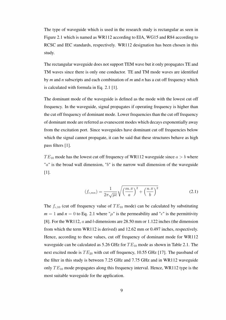
The type of waveguide which is used in the research study is rectangular as seen in
Figure 2.1 which is named as WR112 according to EIA, WG15 and R84 according to
RCSC and IEC standards, respectively. WR112 designation has been chosen in this
study.
The rectangular waveguide does not support TEM wave but it only propagates TE and
TM waves since there is only one conductor. TE and TM mode waves are identified
by m and n subscripts and each combination of m and n has a cut off frequency which
is calculated with formula in Eq. 2.1 [1].
The dominant mode of the waveguide is defined as the mode with the lowest cut off
frequency. In the waveguide, signal propagates if operating frequency is higher than
the cut off frequency of dominant mode. Lower frequencies than the cut off frequency
of dominant mode are referred as evanescent modes which decays exponentially away
from the excitation port. Since waveguides have dominant cut off frequencies below
which the signal cannot propagate, it can be said that these structures behave as high
pass filters [1].
TE10 mode has the lowest cut off frequency of WR112 waveguide since a > b where
"a" is the broad wall dimension, "b" is the narrow wall dimension of the waveguide
[1].
(fc,mn) =1
2π√με
√(m.π
a
)2
+(n.π
b
)2
(2.1)
The fc,10 (cut off frequency value of TE10 mode) can be calculated by substituting
m = 1 and n = 0 to Eq. 2.1 where "μ" is the permeability and "ε" is the permittivity
[8]. For the WR112, a and b dimensions are 28.50 mm or 1.122 inches (the dimension
from which the term WR112 is derived) and 12.62 mm or 0.497 inches, respectively.
Hence, according to these values, cut off frequency of dominant mode for WR112
waveguide can be calculated as 5.26 GHz for TE10 mode as shown in Table 2.1. The
next excited mode is TE20 with cut off frequency, 10.55 GHz [17]. The passband of
the filter in this study is between 7.25 GHz and 7.75 GHz and in WR112 waveguide
only TE10 mode propagates along this frequency interval. Hence, WR112 type is the
most suitable waveguide for the application.
9

2.1.1 Waveguide Flanges
At the end of the waveguides there should be flanges that connect the surfaces be-
tween two seperate waveguide structures. The shape of these flanges are mostly
square; however, they can also be circular or rectangular. There are also IEC, EIA
and RCSC standards for flange dimensions as in waveguides. For the connection of
two flanges generally four bolts are used in each corner, but there can also be addi-
tional pins or bolts to increase accuracy of alignment. These flange structures may
comprise o-rings and Choke Flanges or they can be Cover Flanges which is just a
plain surface as shown in Figure 2.2. If the surface of cover flange is clean, smooth
and square, RF power leakage would not be much and VSWR value would be typ-
ically less than 1.03. If there is any imperfection at the contact, voltage breakdown
can occur for high power applications [1].
Figure 2.2: Rectangular waveguide cover flange
O-ring is a torus shaped elastic material product which is put into the groove on the
waveguide flanges. It creates a sealing between two connecting ports in terms of air
permeability. Reason for using o-ring is to create a pressurized environment inside to
avoid moisture to enter in the waveguide. Hence, o-ring increases the power that can
be carried through the waveguide by increasing the breakdown voltage.
Choke flange is an another standard flange type which has an increased breakdown
voltage level. For the connection, one joining part should be a cover flange and the
10

other one should be a choke flange as shown in Figure 2.3. In the choke flange part,
incident wave firstly encounters a λg/4 opening which is parallel to the contact sur-
face and this gap behaves as open circuit. Hence, any resistance in this part becomes
series with a very high resistance which reduces its effect. After that, second λg/4
gap (the one that is localized along waveguide) comes across which behaves as a
short circuit, so the high impedance in the contact surface is transformed into very
low impedance. With this structure, an effective low resistance path is created for the
current flow, and voltage breakdown is avoided. Locations of these λg/4 openings are
shown in Figure 2.3. Due to its breakdown advantages, cover to choke flange con-
nection is mostly preferred in high power applications. On the other hand, frequency
dependence of this connection type is high as compared to the cover to cover flange
connection since choke dimension depends on λg. Its VSWR value is typically lower
than 1.05 [1].
Figure 2.3: Cover to cover and cover to choke flange connections [1]
In the light of these knowledge, cover flange is suitable for our application since the
maximum power requirement for the waveguide filter is 500 W. Furthermore, the
area which the waveguide filter will be placed is inside the radome, which will be
pressurized by a waveguide dehydrator, the usage of o-ring is not necessary.
11

2.2 Electronic Filters
Aim of the electronic filters is basically eliminating undesirable frequency ranges
from the signals. They are two port networks which provide transmission with an
insertion loss at the specified pass band and attenuation in the desired stop band. One
port is defined as input and the other one is output which can be interchanged since
the system is reciprocal [9].
For this purpose, low pass, high pass, bandpass or band stop filters whose charac-
teristics are given in Figure 2.4 may be built. Among these types, bandpass filter is
realized due to design specifications. However, the design starts with a low pass pro-
totype, after that by scaling the circuit elements bandpass filter response is obtained
[2].
Figure 2.4: Low pass, bandpass, high pass, band stop filters
Attenuation is defined in logarithmic units for the filters and the conversion formula
is given in Eq. 2.2.
12

AttenuationdB(f) = 20 log10
[Input Voltage(f)
Output Voltage(f)
](2.2)
Return loss, insertion loss and isolation (Eqs. 2.3 and 2.4 [1, 9]) determines the filter
specifications. Return loss is checked from reflection parameter, S11. In the passband
of the filter, this value should be as high as possible and it is vice versa for the stop
band. On the other hand, insertion loss which should be as low as possible in the pass
band is determined by transmission parameter, S21. Isolation is also determined by
S21, but it is the value of rejection of the undesired frequencies, hence, it should be
higher in the stop band.
Return loss = 20 log10 |S11| (2.3)
Insertion loss = 20 log10 |S21| (2.4)
Filter blocks or elements are typically ideal inductors and capacitors at low frequen-
cies; however, at microwave frequencies, a more involved model namely distributed
elements should be used. At low frequencies there is a complete and simple syn-
thesis procedure, while at the microwave frequencies there is not an exact theory or
synthesis procedure due to complex frequency characteristics of microwave circuit
elements, which makes the design more challenging. Despite this complication, there
are several techniques that can be used to design microwave filters [8].
There are two main methods for microwave filter design which are the image param-
eter and insertion loss method. Image parameter method was initially used in filter
design for low frequency radio and telephony in the late 1930s. In image parameter
method, two port simple filter sections are connected to get desired cut off frequency
and attenuation; however, a full band frequency characteristic cannot be obtained and
it requires many iterations to get the final result [1].
Insertion loss method is mostly used for the filters which have specific frequency
responses. It is a technique based on network synthesis and it starts with a normalized
low pass prototype in terms of cut off frequency and impedance. Later on to get
13
desired filter characteristics, transformations in terms of impedance and frequency
should be used [1].
In both methods, resultant designs are the combination of capacitors and inductors.
Eventually, for the implementation of microwave filters some other transformations
such as impedance inverters, admittance inverters, Kuroda identities or Richard’s
transformation are required [1]. These transformations convert lumped elements
to practical components such as stubs, transmission lines sections and resonant el-
ements. For the realization of bandpass and bandstop filters impedance (K) and ad-
mittance (J) inverters are used [18].
In the design of filters in this thesis work, insertion loss method has been used be-
cause of its advantages explained above. The design process will be covered in the
following sections starting from low pass prototype to symmetrical iris waveguide
filter parameters.
2.2.1 Insertion Loss Method
In the insertion loss method, designer can choose the response type according to the
application. If the requirement is lowest insertion loss, Maximally Flat (Butterworth)
response can be used. If sharpest cut off is important, Chebyshev (Equiripple) re-
sponse would be the most suitable one [1, 18]. In this design, since the higher cut
off is 7.75 GHz and 70 dB attenuation is required at 7.9 GHz, a sharp attenuation
characteristic for the upper side is more crucial. Moreover, if the order of the filter
is increased, steepness of the skirts increase. Thus, at the same frequency, a higher
isolation level is seen. For this reason, Chebyshev response is used for the design
[1, 18].
Design steps will be;
• Lowpass filter prototype synthesis
• Transformation to bandpass filter
• Waveguide filter structure synthesis
14
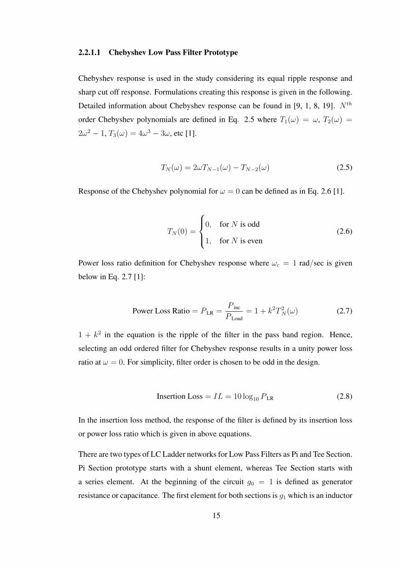
2.2.1.1 Chebyshev Low Pass Filter Prototype
Chebyshev response is used in the study considering its equal ripple response and
sharp cut off response. Formulations creating this response is given in the following.
Detailed information about Chebyshev response can be found in [9, 1, 8, 19]. N th
order Chebyshev polynomials are defined in Eq. 2.5 where T1(ω) = ω, T2(ω) =
2ω2 − 1, T3(ω) = 4ω3 − 3ω, etc [1].
TN(ω) = 2ωTN−1(ω)− TN−2(ω) (2.5)
Response of the Chebyshev polynomial for ω = 0 can be defined as in Eq. 2.6 [1].
TN(0) =
⎧⎪⎨⎪⎩0, for N is odd
1, for N is even
(2.6)
Power loss ratio definition for Chebyshev response where ωc = 1 rad/sec is given
below in Eq. 2.7 [1]:
Power Loss Ratio = P LR =P inc
P Load
= 1 + k2T 2N(ω) (2.7)
1 + k2 in the equation is the ripple of the filter in the pass band region. Hence,
selecting an odd ordered filter for Chebyshev response results in a unity power loss
ratio at ω = 0. For simplicity, filter order is chosen to be odd in the design.
Insertion Loss = IL = 10 log10 P LR (2.8)
In the insertion loss method, the response of the filter is defined by its insertion loss
or power loss ratio which is given in above equations.
There are two types of LC Ladder networks for Low Pass Filters as Pi and Tee Section.
Pi Section prototype starts with a shunt element, whereas Tee Section starts with
a series element. At the beginning of the circuit g0 = 1 is defined as generator
resistance or capacitance. The first element for both sections is g1 which is an inductor
15

or capacitor according to the circuit model. Then the following elements denoted by
gk can be found as in the Eq. 2.15 using Eq. 2.9 to Eq. 2.14 from 2nd to N th element.
The last element at the end is defined as gN+1 which is the load resistance if gN is a
shunt capacitor and load conductance if gN is a series inductor [1]. The type of the
prototype used in the design of the filter is Pi Section as in Figure 2.5
Figure 2.5: Pi section low pass prototype filter circuit configuration
The Chebyshev low pass filter prototype element values are given by the following
formulas where N is the filter order [8, 9]:
ε =
√10
⎛⎝RPdB
10
⎞⎠− 1, (2.9)
β = ln
√1 + ε2 + 1√1 + ε2 − 1
, (2.10)
γ = sinh
(β
2N
), (2.11)
ak = sin
(2k − 1
2Nπ
), (2.12)
bk = γ2 + sin2
(kπ
N
)for (k=1,2,...,N ) (2.13)
Once ak and bk are determined, the element values can be obtained starting with g1
from 2.14 and continue till gN+1 with Eqs. in 2.14, 2.15 and 2.16 [9].
g1 =2a1γ
, (2.14)
16

gk =4ak−1akbk−1gk−1
for (k=2,3,...,N ), (2.15)
gN+1 =
⎧⎪⎨⎪⎩1, for N is odd
tanh2
(β
4
), for N is even
(2.16)
2.2.1.2 Low Pass to Band Pass Transformation
As mentioned before, low pass prototype is transformed to bandpass as a next design
step. To do this, inductors and capacitors must be scaled as bandpass elements as
shown in Figure 2.6. Inductors and capacitors become resonating LC circuit elements
at center frequency, ω0 [9].
Figure 2.6: Low pass filter prototype to bandpass transformation
To scale the frequency, Eq. 2.17 is used [9] where;
• ω0 =√ω1ω2 is the center frequency
• ω1 is the lower cut off frequency
• ω2 is the upper cut off frequency
17

ω′= fbandpass(ω) =
ω0
ω2 − ω1
(ω
ω0
− ω0
ω) (2.17)
Transformed inductor impedance takes the form given in Eq. 2.18 and has the same
form as the impedance of a series LC circuit as given in Eq. 2.19 [9].
jωLLP → jω0
ω2 − ω1
(ω
ω0
− ω0
ω)LLP (2.18)
Thus, inductors in the low pass prototype are transformed into series LC resonators
(Eq. 2.19) and capacitors are replaced by parallel LC circuits [9].
jωLBP = jωLBPofL +1
jωCBPofL
(2.19)
where:
• LBPofL =LLP
ω2 − ω1
• CBPofL =ω2 − ω1
ω20LLP
Similarly, a capacitor in the low pass prototype is transformed into a parallel LC
circuit and the corresponding LBPofC and CBPofC values are given in Eq. 2.20 and
Eq. 2.21 [9].
LBPofC =ω2 − ω1
ω20CLP
(2.20)
CBPofC =CLP
ω2 − ω1
(2.21)
Since the low pass prototype is normalized to 1Ω, at the end impedance should also
be scaled by dividing capacitances and multiplying inductances by RLoad which is
50Ω in our case.
18

2.2.1.3 Conversion of Bandpass Structure to a Realizable Circuit Model
After low pass to bandpass transformation, a network is created with both series and
shunt LC resonators as seen in Figure 2.7-(a) [9]. At this step, since there are only
impedance, inductor and capacitors in the network, waveguide filter dimensions can
not be realized yet. The chosen filter structure is shunt inductance symmetrical iris
which will be explained in the following parts. Hence, in order to get physical dimen-
sions, structure should only consists of shunt inductances which will be realized as
irises and transmission lines that will give cavity lengths.
To obtain a circuit that has only series/shunt elements, Kuroda identities or impedance
(K)/admittance (J) inverters can be used. These inverters are useful for bandpass
and bandstop filters that have narrow (<%10) bandwidths like in this case (%6.67).
K-inverters inverts the load impedance to admittance and vice versa for J inverters
[1]. Thus, first, to get rid of shunt LC resonators, K impedance inverters are used
which are seen in the network in Figure 2.7-(b). K-Inverters formulations are given in
Eqs. 2.22, 2.23 and 2.24. Further information about calculations can be found in [9].
K01 =
√RAL0ω0δω
g0g1ω′1 (2.22)
Kj,j+1 =δω
ω′1
√L20ω
20
gjgj+1
where (j=1,2,...,N − 1) (2.23)
KN,N+1 =
√RBL0ω0δω
gNgN+1
ω′1 (2.24)
But, the structure in Figure 2.7-(b) is still not appropriate for waveguide filter real-
ization since there are series LC elements. In order to eliminate series LC resonators,
another inversion is conducted to convert series LC resonators into half-wave trans-
mission line models with Z0 impedance by using reactive slope parameters of series
LC resonators and half wave short circuited transmission lines [19]. This conversion
is based on the equivalence between the reactive slope parameters of half wave short
circuited transmission line and series lumped element resonator which is only valid
19
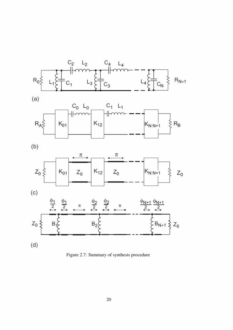
Figure 2.7: Summary of synthesis procedure
20

when the load impedance of both circuits are low. The reactive slope parameter of
series LC is ω0L and this parameter replaced byπ
2Z0, reactive slope parameter of half
wavelength transmission line. Resultant circuit scheme is shown in Figure 2.7-(c) [9].
Lastly, K inverters are converted into more practical structures as reactive elements,
shunt inductances, cascaded with two transmission lines with negative electrical length,
φ/2 as in Eq. 2.25, which is shown in Figure 2.7-(d) [1, 9, 18].
φ = −tan−1 2
B(2.25)
Total electrical length giving the dimension of waveguide cavities are sum of π ob-
tained from realising series LC resonators, and φi/2+φi+1/2 coming from realisation
of K inverters [19].
2.3 Waveguide Filters
Waveguide filters are very useful for microwave frequency applications when low
insertion loss and high isolation are required. Waveguide filter technology is widely
preferred and it has been used in different applications after World War II.
If identical reactive obstacles like irises or posts are put into waveguides, they are
called as periodic structures. There are many forms of periodic structures depending
on the used transmission line media [1].
There is a wide variety of reactive elements which can be used as obstacles in order
to get desired response. However, the most common reactive elements are irises and
posts that can be used as both inductive and capacitive elements depending on their
positions, sizes and geometries [9].
In this study, shunt inductive symmetrical irises are used as reactive elements. This
structure is very suitable since it has high efficiency and can be easily manufactured
in waveguide structures [19]. Irises are thin metallic diaphragms which are located
parallel to the transverse electric field of dominant TE10 mode, in other words in
the E-Plane of the waveguide (Figure 3.9) [9]. In this study, the thickness of the
21

diaphragms is chosen to be 0.5 mm for manufacturability and mechanical strength.
2.3.1 Dimension Calculation for Iris Aperture Width
There are many discontinuity types which can be placed in waveguides as reactive
elements. Their reactance values depend on their locations in the waveguide as men-
tioned before. The most common structures are shunt inductance symmetrical and
non symmetrical iris, shunt capacitance symmetrical and non symmetrical iris, shunt
inductive post and shunt capacitive post which are shown in Figure 2.8 [19].
Figure 2.8: Most Common Discontinuity Types [9]
22

For the current design, E plane symmetrical iris structure is preferred as shunt induc-
tors which is also known as H plane waveguide filter [14]. This structure is named as
shunt inductance symmetrical iris and the most accurate one in terms of bandwidth,
return loss and center frequency responses and also it is easy to implement [19]. Thus,
it is mostly chosen in waveguide filter applications.
The geometry of shunt inductor symmetrical iris structure is given in Figure 2.9
Figure 2.9: Shunt inductive symmetrical iris structure
Formula for the susceptance created by the opening between symmetrical irises is
given in Eq. 2.26 [9]. However, this is an empirical formula; therefore, there are
many variations of it in the literature.
B =2π
βacot2
(πd
2a
)[1 +
aγ3 − 3π
4πsin2
(πd
a
)](2.26)
where,
β =
√ω2εμ−
(πa
)2
, γ3 =
√(3π
a
)2
− ω2εμ (2.27)
For the design, expression for B is simplified as in Eq. 2.28 which is also found in
the literature [20]. d dimension shown in Figure 2.9 is derived from Eq. 2.28.
B =2π
βacot2
(πd
2a
)(2.28)
23

d values are found theoretically with the Eq. 2.28 for zero thickness diaphragms;
however, practically it is not possible to have zero thickness [9]. In the designed
filter, this thickness value is 0.5 mm due to fabrication restrictions.
2.3.2 Dimension Calculation for Waveguide Cavity Length
For the final realisation of shunt inductance symmetrical iris structure which is shown
in Figure 2.10, waveguide cavity lengths should also be found.
Figure 2.10: Dimensions of symmetrical iris waveguide filter
Length �iin Figure 2.10 is the distance between two consecutive irises namely waveg-
uide cavity lengths. �i, waveguide cavity lengths, can be found using the formula
given in Eq. 2.29 [9].
�i =λg0
2π
(π +
φi
2+
φi+1
2
)(2.29)
φi/2 and φi+1/2 seen in Eq. 2.29 is the electrical lengths of transmission line sections
with negative lengths at two sides of shunt inductances shown in Figure 2.7. The total
electrical length between two consecutive irises are π +φi
2+
φi+1
2.
24

CHAPTER 3
WAVEGUIDE FILTER DESIGN
Using Computer Aided Design (CAD) tools such as Ansoft-HFSS or CST Microwave
Studio makes the design process faster and decrease the need for manufactured pro-
totypes. However, these tools cannot always calculate the inevitable variations due
to different component characteristics and manufacturing tolerances. Moreover, there
can be differences between CAD results and measurement results of the product ow-
ing to surface roughness, discontinuities, accuracy of the measuring components, etc.
As a result, tuning is likely to be needed at the end of manufacturing process [1].
Ansoft-HFSS is the main CAD tool used in this current study, and CST Microwave
Studio is also used to compare the simulation results of the final design.
Shunt inductance symmetrical iris waveguide filter design consists of the following
steps;
• Dimension calculation
• CAD tool simulation
• Optimization
• Manufacturing
• Tuning
Two different designs are considered in this work, the first one is 13th order and the
second one is 15th order symmetrical iris filter. Both designs are completed by fol-
lowing the steps mentioned above. In the following sections, modelling of the filter
25
in ANSYS-HFSS tool, optimization study, comparison with CST tool, manufactur-
ing aspects, measurement techniques, agreement of simulation and measurement and
tuning work are explained.
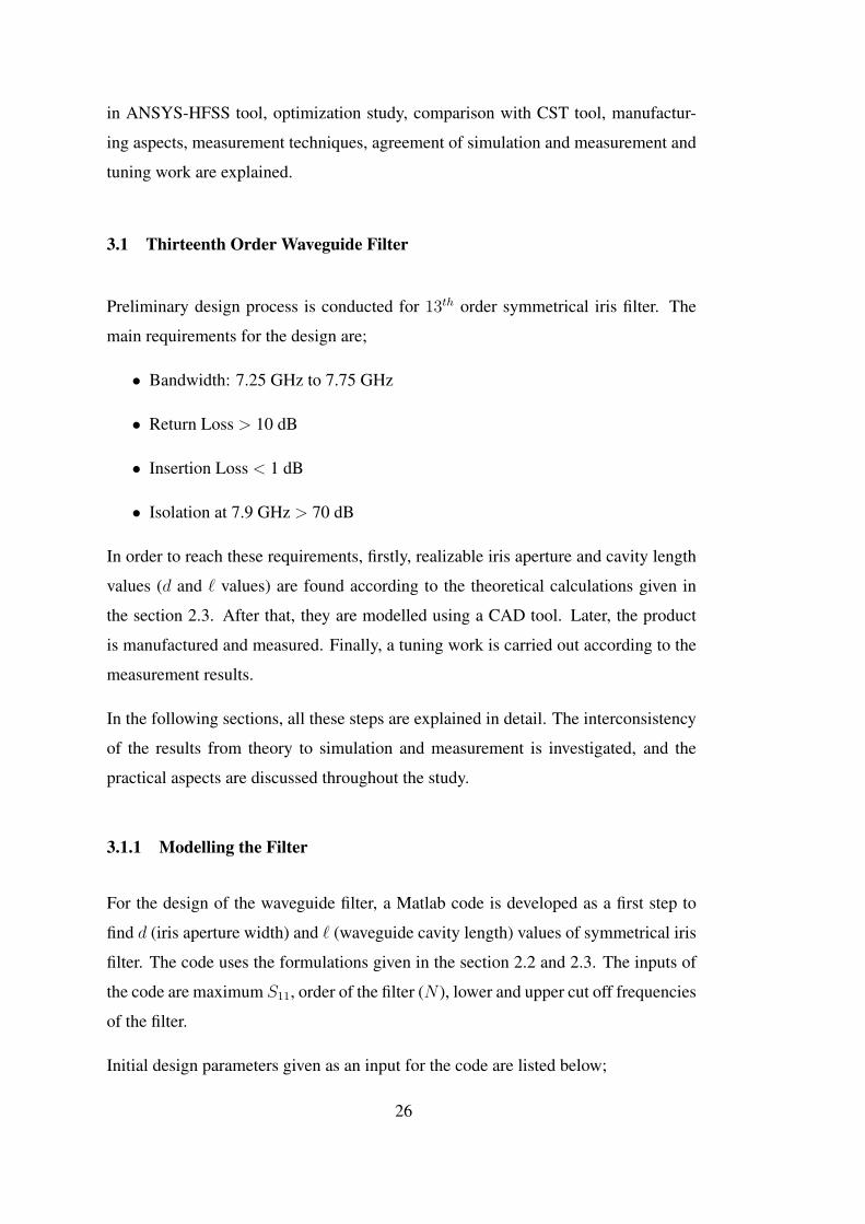
3.1 Thirteenth Order Waveguide Filter
Preliminary design process is conducted for 13th order symmetrical iris filter. The
main requirements for the design are;
• Bandwidth: 7.25 GHz to 7.75 GHz
• Return Loss > 10 dB
• Insertion Loss < 1 dB
• Isolation at 7.9 GHz > 70 dB
In order to reach these requirements, firstly, realizable iris aperture and cavity length
values (d and � values) are found according to the theoretical calculations given in
the section 2.3. After that, they are modelled using a CAD tool. Later, the product
is manufactured and measured. Finally, a tuning work is carried out according to the
measurement results.
In the following sections, all these steps are explained in detail. The interconsistency
of the results from theory to simulation and measurement is investigated, and the
practical aspects are discussed throughout the study.
3.1.1 Modelling the Filter
For the design of the waveguide filter, a Matlab code is developed as a first step to
find d (iris aperture width) and � (waveguide cavity length) values of symmetrical iris
filter. The code uses the formulations given in the section 2.2 and 2.3. The inputs of
the code are maximum S11, order of the filter (N ), lower and upper cut off frequencies
of the filter.
Initial design parameters given as an input for the code are listed below;
26

• S11,max = −20 dB,
• Order of Filter (N )= 13
• Lower Cut Off Frequency (f1)=7.25 GHz
• Upper Cut Off Frequency (f2)=7.75 GHz
The initial values of di and �i obtained using the empirical formulas are listed in Table
3.1. The next step is simulating the waveguide filter using an EM solver. During
simulations an optimization can be necessary in order to ensure requirements.
d1 = d14 14.70 mm �1 = �13 22.82 mm
d2 = d13 9.58 mm �2 = �12 25.52 mm
d3 = d12 8.27 mm �3 = �11 26.00 mm
d4 = d11 8.01 mm �4 = �10 26.10 mm
d5 = d10 7.92 mm �5 = �9 26.14 mm
d6 = d9 7.88 mm �6 = �8 26.15 mm
d7 = d8 7.87 mm �7 26.16 mm
The filter structure which is shown in Figure 3.1, is created in ANSYS-HFSS using
the initial values obtained from the code. The limitations arise by the manufacturing
process are also included in the model such as the iris thickness which is taken as
0.5 mm and chamfers with 1 mm radius at the top and bottom of the irises.
27
Table 3.1: Initial d (iris aperture width) and � (cavity length) dimensions

Figure 3.1: HFSS model of 13th order filter
In the ANSYS-HFSS model, all design parameters are defined as variables so that
parametric sweep (changing only specified parameters while fixing the others) and
optimization over these parameters can be done. Moreover, Perfect Electric Conduc-
tor (PEC) is chosen as the material for filter walls, while inside is defined as air. After
creating the design and making validation check for the 3D geometry, a simulation
set up needs to be generated. There are some significant input parameters of the set
up. First, solution frequency should be given as the highest frequency at which the
S parameters will be simulated. According to this value, an initial mesh is created;
then refinement is done between calculated S parameters iteratively. Maximum num-
ber of passes is chosen as 20 as seen in Figure 3.2 which shows the number of steps
will be conducted during the mesh refinement process. Last, maximum delta S gives
the projected maximum error ratio of the S parameters with the previous one which
is chosen as 0.5% for the simulation as shown in Figure 3.2. If the maximum delta S
target is reached before 20th pass simulation starts or if the target is still not reached
at the 20th pass, it also starts with the final mesh. Generated simulation set up sweeps
from 7 GHz to 8.5 GHz with a step size of 0.01 [21].
The sweep type of the simulation must also be chosen while creating a the set up.
Alternatives are discrete, interpolating and fast sweeps. A sweep type is initially
chosen as "fast" in order to get quick results; however, once an acceptable result is
obtained, it is verified by "interpolating" and "discrete" sweeps, as well. By doing
this, three sweep types are compared.
28

Figure 3.2: HFSS model solution setup
29
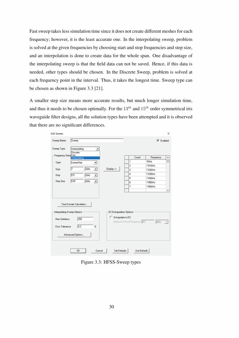
Fast sweep takes less simulation time since it does not create different meshes for each
frequency; however, it is the least accurate one. In the interpolating sweep, problem
is solved at the given frequencies by choosing start and stop frequencies and step size,
and an interpolation is done to create data for the whole span. One disadvantage of
the interpolating sweep is that the field data can not be saved. Hence, if this data is
needed, other types should be chosen. In the Discrete Sweep, problem is solved at
each frequency point in the interval. Thus, it takes the longest time. Sweep type can
be chosen as shown in Figure 3.3 [21].
A smaller step size means more accurate results, but much longer simulation time,
and thus it needs to be chosen optimally. For the 13th and 15th order symmetrical iris
waveguide filter designs, all the solution types have been attempted and it is observed
that there are no significant differences.
Figure 3.3: HFSS-Sweep types
30

When simulation is completed, several post processing tools can be used. In order
to see filter characteristics in terms of isolation, insertion loss and return loss, trans-
mission parameter (S21) and reflection parameter (S11) need to be reviewed (since the
system is reciprocal S11 = S22 and S21 = S12). For the 13th order filter, results in
Figure 3.4 are obtained.
Figure 3.4: 13th order filter response in HFSS according to initial dimensions listedin Table 3.1
Although the initial design is quite close to the desired response, it does not satisfy
all the design criteria as can be seen from Figure 3.4. Bandpass filter characteristics
are obvious; yet, lower cut off is 0.16 GHz higher than the desired value (i.e. band-
width is narrower), and return loss is not as high as desired. An optimization is
carried out by changing the input parameters of the filter geometry calculation code.
For example, since the lower cut off is higher (7.41 GHz) than the expected result
31

(7.25 GHz), the value of this frequency in the code is decreased as much as the differ-
ence (7.41 GHz−7.25 GHz=0.16 GHz) and the simulation is run again with the new
d and � values. This process is maintained by changing necessary frequency values
and maximum S11 input of the code until a satisfactory result is obtained.
Due to nonidealities, results differ from the theoretical calculations. Some of these
nonidealities are modelled in ANSYS-HFSS to see their effect and optimize the re-
sults by taking them into consideration before manufacturing. These nonidealities are
explained in the section 3.1.3.
3.1.2 Optimization
The result of the code creates a shifted bandpass filter character. However, to get bet-
ter result, an optimization is done in ANSYS-HFSS program by running parametric
sweeps and optimization tool.
There are too many variables which are the input of the optimization (7 iris aperture
width values from d1 to d7 due to symmetry and 8 cavity length values from �0 to �7).
To find better starting point for optimization and reduce the total run time, parametric
sweeps over each variable (around the values obtained from the code) are carried out.
The optimization algorithm of ANSYS-HFSS is then started from this initial point.
Optimization goals are defined as;
• S21 ≤ −70 dB in the frequency calculation range of 7.85 GHz to 7.95 GHz,
• S21 ≥ −0.5 dB in the frequency calculation range of 7.28 GHz to 7.72 GHz,
• S11 ≤ −10 dB in the frequency calculation range of 7.25 GHz to 7.75 GHz.
The dimensions of the optimization result for the first prototype which is manufac-
tured are given in Table 3.2. Due to the manufacturing tolerance limit which is 20 mi-
cron, only two fractional digits are retained.
The final result obtained after optimization is shown in Figure 3.5 for both PEC and
aluminum material. During the optimization process, it has been observed that if the
insertion loss characteristic gets better, isolation at 7.9 GHz or lower and upper cut
32

d1 = d14 16.92 mm �1 = �13 22.01 mm
d2 = d13 11.14 mm �2 = �12 25.01 mm
d3 = d12 9.81 mm �3 = �11 25.78 mm
d4 = d11 9.35 mm �4 = �10 25.93 mm
d5 = d10 9.21 mm �5 = �9 25.99 mm
d6 = d9 9.20 mm �6 = �8 26.01 mm
d7 = d8 9.20 mm �7 26.02 mm
off frequencies become worse and vice versa. Hence, the best optimization for all the
parameters are aimed. In the final result for 13th order filter, the main goal is restricted
to obtain the right operating bandwidth with at least 10 dB return loss throughout the
band. The aim in 13th order filter is to reach acceptable results and compare them
with the measurement of the manufactured filter.
Figure 3.5: 13th order filter response for PEC and aluminum according to final di-mensions listed in Table 3.2
33
Table 3.2: Final d (iris aperture width) and � (cavity length) dimensions

The differences between material definitions, PEC and aluminum can also be ob-
served in Figure 3.5. The dashed blue lines in the Figure 3.5 show the results of PEC,
and the red lines indicate the results of aluminum material. It can be observed from
the markers that the additional insertion loss due to finite conductivity of aluminum is
about 1 dB at lower frequencies and about 0.6 dB at higher frequencies. In the middle
of the pass band, it is observed that worst insertion loss in the PEC is 0.4 dB, while
it is 0.64 dB for the aluminum. The return loss is higher than 10 dB almost whole
band. Since PEC is an ideal material, aluminum results are more realistic. Hence,
this nonideal yet realistic material is used throughout the following simulations.
3.1.2.1 Simulation Comparison
Final design obtained in ANSYS-HFSS program are transferred to CST Microwave
Studio and simulated using this tool as well. The material used in the simulation is
aluminum. The results of these two simulations are given in Figure 3.6.
Figure 3.6: Manufactured 13th order filter - ANSYS-HFSS and CST Microwave Stu-dio simulation results
S11 calculated by both software are below 10 dB and similar to each other. In the up-
per frequency, there is approximately 5 MHz difference between ANSYS-HFSS and
CST Microwave Studio. The upper corner frequency in HFSS is 7.76 GHz whereas it
is 7.754 GHz in CST. The primary difference between results of the two software is
34
in the lower cut off frequency. Lower cut off frequency is at about 7.21 GHz in CST,
whereas it is at 7.26 GHz in HFSS, which is the most distinctive difference. Inser-
tion loss values are similar in the middle band at about 0.65 dB maximum for both
CST and HFSS. After comparing these results with the measurements, the tool giving
better approximation is investigated. Comparison of simulation and measurement is
given in the section 3.1.4.
3.1.3 Manufacturing
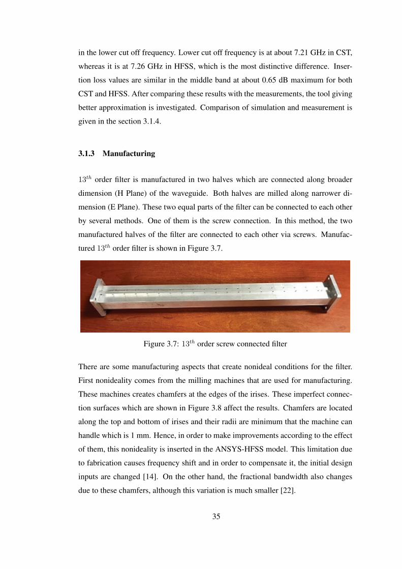
13th order filter is manufactured in two halves which are connected along broader
dimension (H Plane) of the waveguide. Both halves are milled along narrower di-
mension (E Plane). These two equal parts of the filter can be connected to each other
by several methods. One of them is the screw connection. In this method, the two
manufactured halves of the filter are connected to each other via screws. Manufac-
tured 13th order filter is shown in Figure 3.7.
Figure 3.7: 13th order screw connected filter
There are some manufacturing aspects that create nonideal conditions for the filter.
First nonideality comes from the milling machines that are used for manufacturing.
These machines creates chamfers at the edges of the irises. These imperfect connec-
tion surfaces which are shown in Figure 3.8 affect the results. Chamfers are located
along the top and bottom of irises and their radii are minimum that the machine can
handle which is 1 mm. Hence, in order to make improvements according to the effect
of them, this nonideality is inserted in the ANSYS-HFSS model. This limitation due
to fabrication causes frequency shift and in order to compensate it, the initial design
inputs are changed [14]. On the other hand, the fractional bandwidth also changes
due to these chamfers, although this variation is much smaller [22].
35

Figure 3.8: Chamfers along irises
Second, filter needs to be fabricated as two pieces as explained in the previous part
in order to be able to mill the irises. If these pieces are identical, the tolerances for
the chamfers and iris thickness are as low as 1 mm and 0.5 mm with the used milling
machine, respectively. For this purpose, filter is divided into two pieces along the
broader dimension (H-plane).
Since, the electric field of the TE10 mode, dominant mode in WR112, is parallel to the
narrow wall of the rectangular waveguide as shown in Figure 3.9, any discontinuity
on this wall changes the boundary condition and disturbs the field distribution more
as compared to the broad wall of the waveguide.
Third, aluminum is selected as the design material due to its good conductivity value
and easy accessibility.
Last, the manufacturing tolerance of the used milling machine is 20 micron for the
filters with these dimensions. Hence, it may affect all d and � values and change the
results of the filter. This is another non perfect condition based upon manufacturing.
On the other hand, there is a high possibility of imperfect surface on the inside walls
of the filter. To eliminate their effect, to reduce insertion loss and to increase filter
performance, silver plating is applied in the interior walls after production, which
makes the structure more conductive and smooth [23].
36
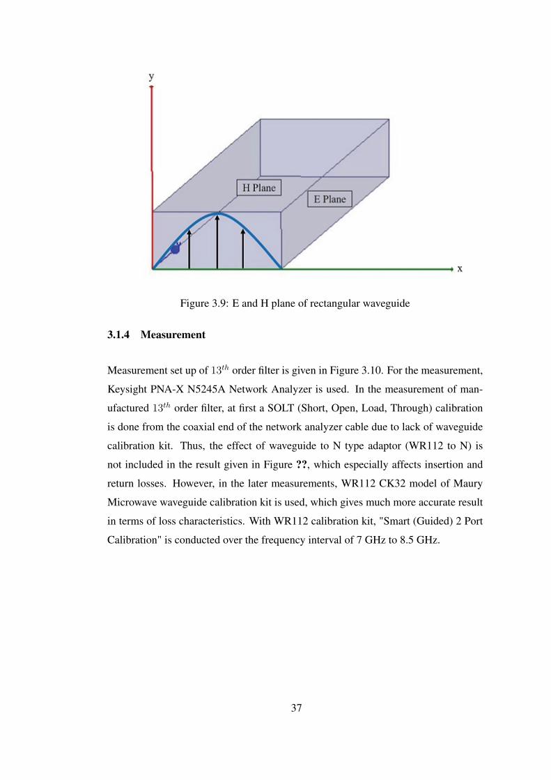
Figure 3.9: E and H plane of rectangular waveguide
3.1.4 Measurement
Measurement set up of 13th order filter is given in Figure 3.10. For the measurement,
Keysight PNA-X N5245A Network Analyzer is used. In the measurement of man-
ufactured 13th order filter, at first a SOLT (Short, Open, Load, Through) calibration
is done from the coaxial end of the network analyzer cable due to lack of waveguide
calibration kit. Thus, the effect of waveguide to N type adaptor (WR112 to N) is
not included in the result given in Figure ??, which especially affects insertion and
return losses. However, in the later measurements, WR112 CK32 model of Maury
Microwave waveguide calibration kit is used, which gives much more accurate result
in terms of loss characteristics. With WR112 calibration kit, "Smart (Guided) 2 Port
Calibration" is conducted over the frequency interval of 7 GHz to 8.5 GHz.
37
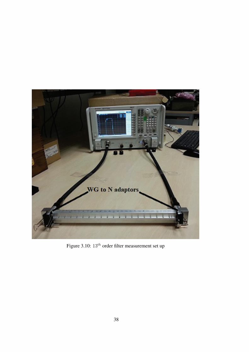
Figure 3.10: 13th order filter measurement set up
38

13th order filter measurement results are compared with HFSS and CST simulation
results in Figure 3.11 in terms of upper and lower cut off frequency and insertion loss.
In the results, it is observed that the lower cut off frequency of the filter is 7.168 GHz
in the measurements which is 7.26 GHz in ANSYS-HFSS simulation and 7.214 GHz
in CST Microwave Studio simulation. Insertion loss, which is about 0.28 dB for
HFSS and 0.5 dB in CST, is higher in measurements (around 1.7 dB). The reason
of the difference of insertion loss is the waveguide to coaxial adapter which is not
included in the calibration process. When isolation at 7.9 GHz is compared with
simulation results, it is about 2 dB lower in the measurements, which may again be
partly due to additional losses from the adapters. Measurement results differs from
simulations mostly in terms of lower cut off frequency. This difference is observed
less in CST Microwave Studio.
Figure 3.11: 13th order filter measurement and simulation results-S21
Return loss is nearly below 10 dB in measurments and its general characteristics are
similar to both the HFSS and CST simulations as seen in Figure 3.12.
Due to known manufacturing impacts, a shift in frequency or bandwidth is inevitable.
As a result, the measured filter characteristics does not satisfy some of the design
criteria. Therefore, tuning screws are added to structure. Thus, use of tuning screws
in the filter for compensation of explained non ideal conditions is necessary [23] .
39

Figure 3.12: 13th order filter measurement and simulation results-S11
3.1.5 Tuning
Tuning screws are inserted at the cavity centers and also at the iris apertures to im-
prove the insertion and return loss, to change the upper cut off frequency and to see
the effect of tuning screws to isolation value at 7.9 GHz [2]. Tuning work is inevitable
for the high order filters like in this case. However, usage of tuning screws creates
additional loss on the filter due to extra added resonant structures and the leakage
from the screw holes.
In practice, off the shelf screws can easily be used in tuning work since they are sim-
ple and practical obstacles although their analysis is very complex. Tuning screw
dimension is chosen as metric 2.5 with 16 mm length so that their penetration can be
adjusted over a wide range. It is easy to adjust their penetration depth and they virtu-
ally behave as a capacitance if r/a value is lower than 0.1 in rectangular waveguides
[24].
Material of the screws is aluminum which can be seen in Figure 3.13. In order to
examine the effect of each tuning screw, 24 of them are placed to the filter. As seen
in Figure 3.13, odd numbered screws are in the middle of iris apertures and even
numbered screws are at cavity centers. Number 4, 14 and 24 cannot be placed in the
manufactured filter since they overlap with the connection screws of filter’s two part.
40

Figure 3.13: Tuning screws in the 13th order filter
41

After examining the effect of all screws, final tuning work is conducted symmetrically
since all the elements are symmetrical in the filter. In the figures, S21 legends (thick
red line) show the untuned result of the filter that the screws are connected to cut
leakage but not turned through the filter. Then, one by one screws are turned into
the filter. In the legend part of the following figures, number of each added screw is
indicated.
To see the results more clear, the effect of the screws to lower, middle and upper band
are investigated separately. These measurements are conducted by WR112 calibration
kit.
3.1.5.1 Tuning Screws at Iris Aperture
Effect of screws at the of iris apertures (odd numbered screws) to upper frequency
band of the filter is seen in Figure 3.14. Tuning work is started from the middle
screws that are screw number 13 and 15 and continued one by one in a symmetrical
order.
Figure 3.14: Effect of odd numbered tuning screws to the upper band of 13th orderfilter
42

It is observed that the upper frequency is moved towards higher level till screw 23
is added. According to the results, the effect of the last four odd numbered screws
(3, 25, 1, 27) are negligible. Upper 3 dB cut-off frequency becomes 7.766 GHz as
compared to the 7.753 GHz before tuning. Thus, it is seen that 13 MHz tuning of
upper frequency is possible with odd numbered screws.
As the upper cut-off frequency increases, the isolation at 7.9 GHz also increases. As
seen in Figure 3.15 the initial isolation level is 68.95 dB and it decreases by approxi-
mately 62.59 dB after tuning.
Figure 3.15: Effect of odd numbered tuning screws to the isolation at 7.9 GHz of 13th
order filter
43

In the middle band, as seen in Figure 3.16 insertion loss and ripple are affected ad-
versely from tuning. This is an expected result owing to metallic structures, that
creates imperfections, are added to the path of the waves. This creates reflective sur-
faces, increases metallic losses and causes leakage from gaps around the screws. First
two screws do not have great effect; however, later ones should be tuned carefully in
order not to influence insertion loss too much. Initial insertion loss value in the middle
of the band is 0.38 dB, while it is 1.38 dB when all screws are added.
Figure 3.16: Effect of odd numbered tuning screws to the middle band of 13th orderfilter
44

It can also be said that after usage of WR112 calibration kit, observed loss is 0.38 dB,
whilst it was 1.72 dB with SOLT calibration kit in the middle of the band. So, cali-
brating all the measurement equipments up to the waveguide flanges is very important
in terms of losses. Moreover, it is also seen that the loss value is better in the mea-
surements than the ANSYS-HFSS and CST Microwave Studio simulations.
Figure 3.17: Effect of odd numbered tuning screws to the lower band of 13th orderfilter
Effects of odd numbered screws are examined for the lower band of the filter, as well.
It can be seen in Figure 3.17. It is observed that lower frequency is decreased as the
screws are added up to the screw 23. The effect of last four odd numbered screws are
negligible again for the lower band of the filter response. While the lower frequency
is initially 7.164 GHz, it decreases to 7.128 GHz when all tuning screws are inserted.
It means that the lower cut-off frequency can be adjusted within a band of 30 MHz
45

by tuning the screws at iris apertures.
Return loss characteristics of the filter are also influenced by tuning to some degree
as seen in Figure 3.18. While tuning the filter, S11 is observed very carefully which
is closely related to insertion loss. Each turn of screws have an impact on insertion
and return loss according to the results, so it is better to use as few number of screws
as possible for the tuning. Again it is seen that first couple of screws do not effect the
return loss much. However, when all screws are used return loss decreases by about
3 dB as seen from the markers in Figure 3.18.
Figure 3.18: Effect of odd numbered tuning screws to the return loss of 13th orderfilter
46

To summarize, the upper frequency can be increased by 13 MHz and the lower cut-
off frequency can be decreased by 30 MHz by using the odd numbered screws. The
required bandwidth is 500 MHz and it can be increased by about 40 MHz by using the
screws located at the iris apertures. It is also seen that, 10 screws that are located to
the central portion of the filter are enough whereas screws numbered 1, 3, 25 and 27
are not necessary. Finally, it is observed that the screws which are located at the iris
apertures provide an increase for bandwidth of the filter approximately by 8% with a
small accompanying change in the center frequency.
3.1.5.2 Tuning Screws at Cavity Center
Screws located in the center of waveguide cavities have also influence on S21 and S11.
The screws located at the cavity centers are numbered with even numbers as seen in
Figure 3.13. However, as mentioned before, screws numbered 4, 14 and 24 are not
located in the filter due to a conflict with connecting screws.
Figure 3.19 shows both upper and lower frequency bands. From the Figure 3.19 it can
easily be observed that frequency is moved towards the lower side at both parts. Once
again, effects of middle screws are far more than the outer ones. For the upper band,
frequency changes from 7.74 GHz to 7.716 GHz and for the lower band, it changes
from 7.2 GHz to 7.164 GHz.
47
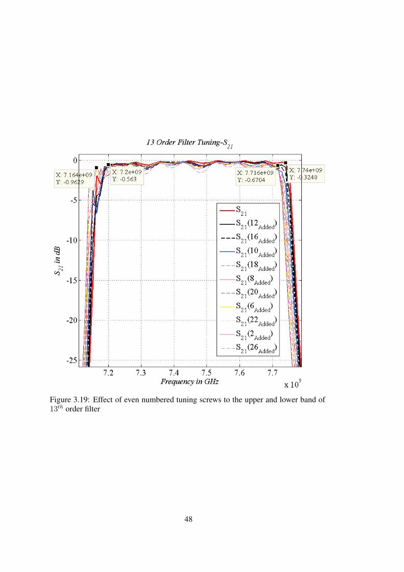
Figure 3.19: Effect of even numbered tuning screws to the upper and lower band of13th order filter
48

Since tuning with even numbered screws shifts whole frequency band to a lower
value, isolation at 7.9 GHz increases as seen in Figure 3.20. While untuned isolation
is 68.95 dB as given before, it becomes 77.13 dB after all screws are adjusted in
tuning.
Figure 3.20: Effect of even numbered tuning screws for isolation at 7.9 GHz
49

Impact of even numbered screws on insertion loss is more than the odd ones as seen
in Figure 3.21. When one tuning screw is added to the structure, insertion loss is
increased about 0.4 dB. But, other screws do not add much loss. On the other hand,
screws numbered 2 and 26 affect the insertion loss considerably as can be observed
from the markers in Figure 3.21.
Figure 3.21: Effect of even numbered tuning screws to the middle band of 13th orderfilter
50
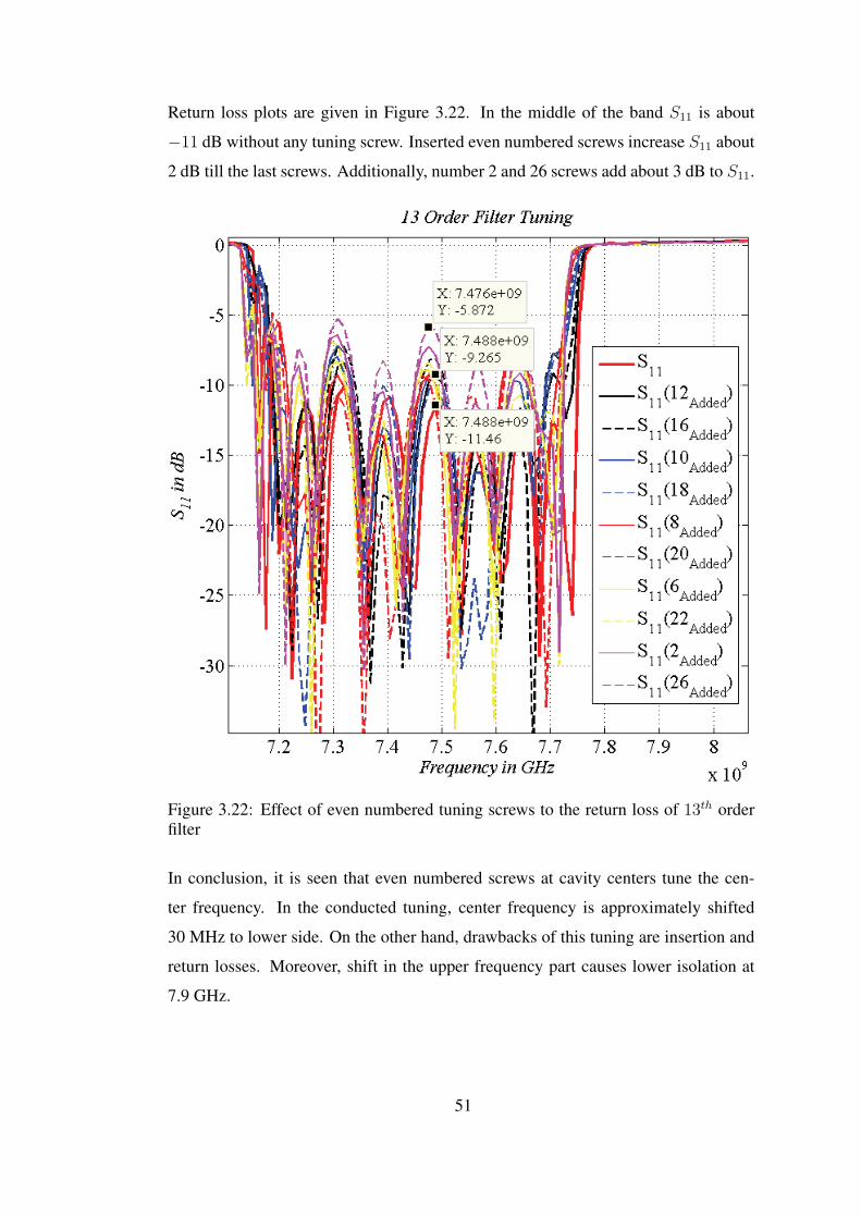
Return loss plots are given in Figure 3.22. In the middle of the band S11 is about
−11 dB without any tuning screw. Inserted even numbered screws increase S11 about
2 dB till the last screws. Additionally, number 2 and 26 screws add about 3 dB to S11.
Figure 3.22: Effect of even numbered tuning screws to the return loss of 13th orderfilter
In conclusion, it is seen that even numbered screws at cavity centers tune the cen-
ter frequency. In the conducted tuning, center frequency is approximately shifted
30 MHz to lower side. On the other hand, drawbacks of this tuning are insertion and
return losses. Moreover, shift in the upper frequency part causes lower isolation at
7.9 GHz.
51

3.2 Fifteenth Order Waveguide Filter
After gaining experience about practical aspects on waveguide filter design, a second
study for 15th order is conducted to obtain better results. Main requirements of 15th
order filter are given below;
• Bandwidth 7.25 GHz to 7.75 GHz
• Return Loss > 20 dB
• Insertion Loss < 0.5 dB
• Isolation at 7.9 GHz > 70 dB
For the 15th order filter, goals about losses i.e. return loss and insertion loss are more
stringent. Moreover, it is almost certain that due to imperfections mentioned before,
tuning will be necessary in this work, as well. So, in order to handle the negative
effects of tuning, order of the filter is increased to 15. Benefit of 15th order is that
there will be a higher isolation level at 7.9 GHz which will be an advantage during
tuning work since some compromises between different requirements is inevitable.
On the other hand, its disadvantage is total length of the filter. While the length of
filter is approximately 39 cm for 13th order filter, it is 43.8 cm for 15th order filter.
Design process of 15th order waveguide filter is same with 13th order one as given
in section 3.1. On the other hand, different manufacturing techniques are tested for
the second filter to compare the performances of these techniques. The effect of the
calibration is also investigated during validation process of 15th order filter. At the
end of measurements, according to the obtained results, the most effective tuning
screws according to their locations are added into the design and the filter is tuned
carefully.
3.2.1 Modelling the Filter
The same computation code is used to find d (iris aperture width) and � (cavity length)
values for 15th order filter. Initial input parameters of the code are given below;
52

• S11 = −45 dB,
• Order of Filter (N)= 15
• Lower Cut Off Frequency (f1)=7.25 GHz
• Upper Cut Off Frequency (f2)=7.75 GHz
According to the experience in 13th order filter design, S11 value is kept very low even
in the first trial. Cut-off frequencies in the input of the code is exactly the required
values, but it is known from the first design that the result will be shifted in frequency
scale. According to the initial results, optimization is conducted by changing the input
values as in the first design. The d and � values attained from the above inputs are
given in Table 3.3. Same procedure in previous part is performed for the modelling of
the filter in ANSYS HFSS tool. Iris thickness and chamfer radius are same with 13th
order filter as 0.5 mm and 1 mm, respectively. Simulation set up is also configured
in the same manner and in all simulations "Fast Sweep" is used since no change is
observed for other types in 13th order filter design.
d1 = d16 17.49 mm �1 = �15 20.75 mm
d2 = d15 11.60 mm �2 = �14 24.45 mm
d3 = d14 9.15 mm �3 = �13 25.60 mm
d4 = d13 8.50 mm �4 = �12 25.88 mm
d5 = d12 8.24 mm �5 = �11 25.99 mm
d6 = d11 8.12 mm �6 = �10 26.04 mm
d7 = d10 8.06 mm �7 = �9 26.06 mm
d8 = d9 8.04 mm �8 26.07 mm
53
Table 3.3: Initial d (iris aperture width) and � (cavity length) dimensions of 15th
orderfilter

Simulation result of 15th order filter with these initial dimensions is given in Figure
3.23. Since the S11 input of the code is given as −45 dB, initial return loss is relatively
lower throughout the frequency band than 13th order filter. Moreover, isolation at
7.9 GHz is very high as 91 dB, although, the upper 3 dB frequency is about 7.77 GHz.
However, lower 3 dB frequency is approximately 7.4 GHz which is 15 MHz higher
than the required value. While tuning for the exact frequency levels, isolation and
return loss characteristics will be affected adversely.
Figure 3.23: 15th order result according to initial dimensions listed in Table 3.3
54

3.2.2 Optimization
Results are firstly tuned manually by changing the inputs of the code as mentioned
before. After obtaining a satisfactory result, an optimization set up is created in
ANSYS-HFSS. For the set up from return loss and insertion loss no compromises
is made. Concession is made on isolation value which is decreased to 80 dB as seen
in the following defined goals for optimization tool;
• S21 ≤ −80 dB in the frequency calculation range of 7.85 GHz to 7.95 GHz,
• S21 ≥ −0.4 dB in the frequency calculation range of 7.28 GHz to 7.72 GHz,
• S11 ≤ −20 dB in the frequency calculation range of 7.25 GHz to 7.75 GHz.
At the end of optimization process that is conducted in ANYSY-HFSS, the dimension
values on the Table 3.4 for d and � are found.
d1 = d16 18.48 mm �1 = �15 20.41 mm
d2 = d15 12.82 mm �2 = �14 24.22 mm
d3 = d14 10.28 mm �3 = �13 25.58 mm
d4 = d13 9.64 mm �4 = �12 25.90 mm
d5 = d12 9.40 mm �5 = �11 26.07 mm
d6 = d11 9.28 mm �6 = �10 26.09 mm
d7 = d10 9.22 mm �7 = �9 26.11 mm
d8 = d9 9.18 mm �8 26.12 mm
3.2.2.1 Simulation Comparison
According to final dimensions given in Table 3.4 simulation is repeated in CST Mi-
crowave Studio in order to compare the results. The outcome of both simulations are
55
Table 3.4: Final d (iris aperture width) and � (cavity length) dimensions of 15th
orderfilter

compared in Figure 3.24.
Figure 3.24: Manufactured 15th order filter HFSS and CST simulation results accord-ing to final dimensions listed in Table 3.4
It is seen that in ANSYS-HFSS simulation, return loss is approximately higher than
15 dB level whereas it is mostly higher than 22 dB in CST. Upper 3 dB frequency level
is at 7.5 GHz in HFSS and 7.743 GHz in CST. Also, while lower cut-off frequency
is 7.25 GHz in HFSS, it is 7.23 GHz in CST. On the other hand, isolation level at
7.9 GHz is same in both simulation tools as 80 dB which is seen from the markers of
Figure 3.24.
56

3.2.3 Manufacturing
Filter is manufactured from aluminum as two equal pieces which is cut from H-plane
as in 13th order filter. Three manufacturing techniques are attempted to make the
connection of these two parts of the filter. These techniques are screw connection,
brazing and laser welding. Screw connection method is the one used in 13th order
filter. In this method two parts of the filter is connected to each other with screws.
Brazing is the second method which uses very thin aluminium material (different
from the one used for production of two parts) for the connection of two pieces. This
whole structure is heated till the melting point of aluminium in the connection surface
and two pieces connect to each other by this melted aluminum. One of the key point
is that the structure is held in a pressurized or vacuumed environment in order to
prevent corrosion during the process. In the third method, laser welding, there is
aluminium welding rod that is located in connection region. That rod is laser welded
to the connection surface with a smaller tolerance than normal welding. Visuals of
the products that are manufactured by these three methods are given in Figure 3.25.
The top one in the Figure is connected with screws, middle one is manufactured by
brazing and the below one is produced by laser welding method.
Figure 3.25: Screw connection, brazing and laser welding manufacturing techniques(from top to bottom)
57

3.2.4 Measurement
Measurement set up of 15th order filter is same as 13th order filter which is given in
Figure 3.10 before. However, WR112 calibration kit is used for all the measurements
of 15th order filter. With WR112 calibration kit "Smart (Guided) 2 Port Calibration"
is conducted for frequency interval of 7 GHz to 8.5 GHz with −15 dB power level.
WR112S30 calibration kit of Maury Microwave is used for all the measurements.
As one of the goal is to compare manufacturing methods where small differences
in the results are expected, to eliminate the possibility of measurement mistake, the
measurements of brazing and laser welding is repeated for 6 times. For this purpose
calibration is also iterated each time.
Figure 3.26: 15th order filter-Consistency of brazing method results according to cal-ibration
The S11 and S21 results of the filter manufactured by brazing method is seen in Figure
3.26 for 6 different calibrations. It is observed that the frequency levels is not changed
much according to calibration. However, especially return loss is affected easily due
to calibration. It differs about 2 dB to 4 dB in the measurements.
The result in the laser welding method is same as brazing one. As seen in Figure 3.27,
only significant difference is observed in return loss, as well.
For sensitive measurements in terms of loss, precision of the calibration and cleanli-
58

Figure 3.27: 15th order filter-Consistency of laser welding method results accordingto calibration
ness of used equipments such as short waveguide or waveguide to coaxial adaptor is
very crucial. Even, moving used coaxial cables of network analyzer changes return
loss slightly. As a result, measurement should be conducted very carefully for reliable
results.
After gaining necessary knowledge about measurement sensibility, results of the 15th
order filter design is compared for all 3 techniques in terms of S21 and S11 in Figure
3.28 and 3.30, respectively.
As seen in the S21 graph in Figure 3.28, 3 dB point at upper frequency is at 7.735 GHz
for screw connection method (black legend), at 7.731 GHz for brazing method (blue
legend) and 7.73 GHz for laser welding method (red legend). Since 7.75 GHz is
a strict requirement for the upper 3 dB frequency, there is a need of tuning for all
methods. However, screw connected filter is the best one in terms of upper 3 dB
frequency.
The lower 3 dB frequency is at 7.15 GHz for screw connection method, at 7.147 GHz
for laser welding method and at 7.141 GHz for brazing method. It is far more lower
than both HFSS and CST simulation results which are nearly 7.25 GHz and 7.23 GHz,
respectively. Although there is 100 MHz difference from the requirement, best pro-
59

Figure 3.28: Comparison of 3 techniques in terms of upper and lower frequency andinsertion loss
duction method among these 3 techniques is screw connection method in terms of
lower 3 dB frequency. Lower frequency is a certain requirement that it should be
lower than 7.2 GHz. Thus, 7.15 GHz for this value is not a problem to tune.
When it is compared in terms of insertion loss in the middle band (around 7.5 GHz),
the value for screw connection is 0.13 dB, it is approximately 0.26 dB for brazing and
around 0.41 dB for laser welding. Levels are even better than both HFSS and CST
simulations which are 0.27 dB for screw connection and brazing methods. The finest
one is once again screw connection method in terms of insertion loss.
Comparison of isolation at 7.9 GHz is given in Figure 3.29. The value is about 76 dB
for screw connection, 77 dB for brazing and 80 dB for laser welding. Laser welding
is the best method with regards to isolation; however, requirement for this value is
70 dB that is ensured in all methods.
60

Figure 3.29: Comparison of 3 techniques in terms of 3 techniques in terms of isolation
Return loss character of the filters manufactured by 3 techniques is seen in Figure
3.30. In the Figure, it is obvious that black legend which belongs to screw connected
method gives the best result which is higher than 20 dB almost everywhere between
7.25 GHz to 7.75 GHz.
61

Figure 3.30: Comparison of 3 techniques in terms of return loss
As a result, best results are obtained for screw connection method according to the
requirements and tuning need is obvious for upper 3 dB frequency which should be
15 MHz higher for the screw connection method. For this purpose according to the
obtained results in section 3.1.5, screws at iris apertures create 13 MHz shift of the
upper frequency to a higher level. It is seen that the outer two screws on both sides
are ineffective for 13th order filter. Hence, in order not to create additional loss, only
10 screws are implemented at in the middle of iris apertures.
3.2.5 Tuning
Tuning screws are inserted to the filter manufactured with screw connection method
as mentioned above. As the upper 3 dB frequency requirement is the main aim of the
tuning, 10 screws are located at iris apertures as shown in Figure 3.31.
The same procedure as in the 13th order filter is applied. First, each screws are added
one by one to see their effect and then a general tuning is conducted with all tuning
screws.
62

Figure 3.31: 15th Order Filter Tuning Screws
63

In Figure 3.32, it is seen that upper 3 dB frequency is moved to 7.739 GHz when all
10 screws are added that is the required result.
Figure 3.32: Effect of tuning screws to upper band of 15th order filter
As upper frequency shifts towards an upper level, isolation at 7.9 GHz becomes lower.
Isolation part of the plot is focused in Figure 3.33. As expected the S21 value at
7.9 GHz become approximately −76 dB while it is about −79 dB at first.
64

Figure 3.33: Effect of tuning screws to isolation at 7.9 GHz of 15th order filter
65

The effect of 10 screws on insertion loss can be observed in Figure 3.34. The differ-
ence in the insertion loss is just 0.02 dB in the middle of the band.
Figure 3.34: Effect of tuning screws to middle band of 15th order filter
66

Since tuning screws are located at iris apertures, a frequency expansion in bandwidth
is expected as in section 3.1.5. Upper frequency is shifted to a higher level as seen
above and the lower frequency is shifted to a lower level as shown in Figure 3.35. The
lower 3 dB frequency is shifted from 7.148 GHz to 7.143 GHz. Hence, bandwidth is
expanded as expected.
Figure 3.35: Effect of tuning screws to lower band of 15th order filter
67

After confirming the effect of all screws, a tuning is performed with all screws. The
aim is to tune upper 3 dB frequency from 7.735 GHz to 7.75 GHz and try not to effect
insertion and return losses much. Before and after tuning results are given in Figure
3.36. Before tuning result are measured when all tuning screw holes are opened on
the filter. Hence, loss values differ from the initial, without holes, results.
As seen from markers, upper 3 dB frequency become 7.749 GHz after tuning which
is swept exactly 14 MHz. Return loss after tuning is affected about 4 dB throughout
the passband. Insertion loss is changed to 0.5 dB from 0.37 dB. At last, lower 3 dB
frequency is become 7.135 GHz at 2 dB whereas it is 7.15 GHz before tuning at the
same level as shown in Figure 3.36.
Figure 3.36: S21 of the 15th order filter before and after tuning
68
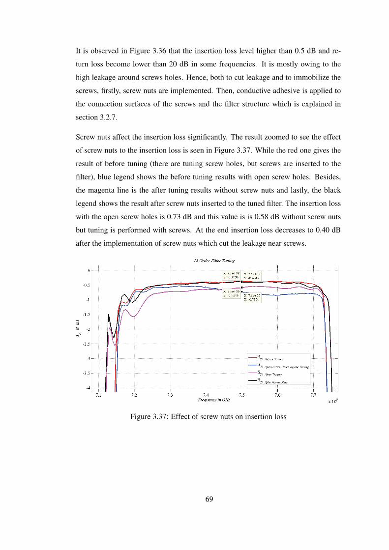
It is observed in Figure 3.36 that the insertion loss level higher than 0.5 dB and re-
turn loss become lower than 20 dB in some frequencies. It is mostly owing to the
high leakage around screws holes. Hence, both to cut leakage and to immobilize the
screws, firstly, screw nuts are implemented. Then, conductive adhesive is applied to
the connection surfaces of the screws and the filter structure which is explained in
section 3.2.7.
Screw nuts affect the insertion loss significantly. The result zoomed to see the effect
of screw nuts to the insertion loss is seen in Figure 3.37. While the red one gives the
result of before tuning (there are tuning screw holes, but screws are inserted to the
filter), blue legend shows the before tuning results with open screw holes. Besides,
the magenta line is the after tuning results without screw nuts and lastly, the black
legend shows the result after screw nuts inserted to the tuned filter. The insertion loss
with the open screw holes is 0.73 dB and this value is is 0.58 dB without screw nuts
but tuning is performed with screws. At the end insertion loss decreases to 0.40 dB
after the implementation of screw nuts which cut the leakage near screws.
Figure 3.37: Effect of screw nuts on insertion loss
69
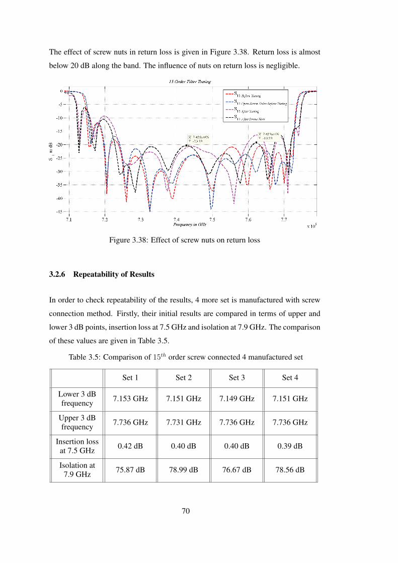
The effect of screw nuts in return loss is given in Figure 3.38. Return loss is almost
below 20 dB along the band. The influence of nuts on return loss is negligible.
Figure 3.38: Effect of screw nuts on return loss
3.2.6 Repeatability of Results
In order to check repeatability of the results, 4 more set is manufactured with screw
connection method. Firstly, their initial results are compared in terms of upper and
lower 3 dB points, insertion loss at 7.5 GHz and isolation at 7.9 GHz. The comparison
of these values are given in Table 3.5.
Set 1 Set 2 Set 3 Set 4
Lower 3 dBfrequency
7.153 GHz 7.151 GHz 7.149 GHz 7.151 GHz
Upper 3 dBfrequency
7.736 GHz 7.731 GHz 7.736 GHz 7.736 GHz
Insertion lossat 7.5 GHz
0.42 dB 0.40 dB 0.40 dB 0.39 dB
Isolation at7.9 GHz
75.87 dB 78.99 dB 76.67 dB 78.56 dB
70
Table 3.5: Comparison of 15th order screw connected 4 manufactured set

As seen in Table 3.5, lower 3 dB frequency oscillates 4 MHz, where maximum dif-
ference is 5 MHz for the upper 3 dB cut off frequency. Insertion loss in at 7.5 GHz is
around 0.40 dB with the same calibration for all 4 set. On the other hand, isolation at
7.9 GHz changes between 75.87 dB to 78. dB. Return losses are all below 20 dB in
the interested band that is 7.25 GHz to 7.75 GHz. According to the results, the most
significant difference is at upper 3 dB frequency of Set 2. It is seen that all filters
produced in the same manufacturing conditions have similar results.
Set 1 Set 2 Set 3 Set 4
Lower 3 dBfrequency
7.133 GHz 7.103 GHz 7.126 GHz 7.119 GHz
InsertionLoss at 7.5
GHz0.29 dB 0.30 dB 0.29 dB 0.29 dB
Isolation at7.9 GHz
71.57 dB 71.73 dB 72.02 dB 70.73 dB
Tuning work is conducted for all 4 sets to set the upper 3 dB frequency to 7.75 GHz.
Obtained values for tuned 4 sets when their upper 3 dB frequencies set to 7.75 GHz
are given in Table 3.6.
As seen in Table 3.6, insertion loss of 4 sets are very similar to each other after inde-
pendent tuning procedures. Isolation is also barely different where all have isolation
at 7.9 GHz higher than 70 dB. On the other hand, lower 3 dB frequency become very
low for set 2 after tuning because of 5 MHz difference from the others for the upper
3 dB frequency in the beginning.
3.2.7 Usage of Conducting Adhesive for Tuning Screws
In order to immobilize the tuning screws and cut the possible leakage near to screws
initially nuts are used as mentioned before. Later, to create a greater fixity and even
lower leakage, usage of conductive adhesive is evaluated. For this purpose, two
thixotropic epoxy conductive adhesive as EJ-2189-LV and EJ-2189 are implemented
to Set 1 and Set 2 filters, respectively that the results are given in section 3.2.6. While
71
Table 3.6: Comparison of 15th order screw connected 4 manufactured set after tuning

implementing adhesives, all connection surfaces and screws are cleaned with alcohol
to create pureness of surfaces which is crucial for the reliability of application.
For Set 1, adhesive is applied to only connection surfaces of screws. Then tuning
work is repeated one more time before curing starts (curing of the adhesive takes 3
days at room temperature which gives couple of hours for tuning). The comparison
of tuning before and after conducting adhesive application for Set 1 is given in Figure
3.39.
Figure 3.39: Effect of Conductive adhesive-Epoxy EJ-2189-LV
As seen in the result, isolation, insertion and return losses are not changed signifi-
cantly. There are 0.03 dB difference in insertion loss, 2 dB difference in isolation at
7.9 GHz and 13 MHz difference in lower 3 dB frequency after conductive adhesive
application. Return loss is very similar except the slight adverse difference in the
middle parts as seen in Figure 3.39.
For Set 2, this time adhesive is applied to all surfaces of the screws. Used product
is slightly different than the first one in terms of thixotropic index but has the same
curing time interval. The comparison of before and after tuning for Set 2 is given in
Figure 3.40.
72

Figure 3.40: Effect of Conductive adhesive-Epoxy EJ-2189
Figure 3.40 shows that there are 0.01 dB difference in insertion loss, 17 MHz discrim-
ination in lower 3 dB frequency and about 2 dB difference in isolation at 7.9 GHz after
the adhesive implementation. Return loss character is slightly better when consider-
ing the whole band after adhesive usage.
After conductive adhesive exercise, tuning is performed over again, these little dif-
ferences may be caused by tuning repetition. Hence, according to comparison graphs
it can be said that conductive adhesive application do not affect the results crucially.
The leakage is cut enough with the connection of screw nuts.
73

74

CHAPTER 4
CONCLUSION
Throughout the study, several aspects are investigated. Initially, a code is written for
synthesis and realization procedure. The dimensions obtained from the code give
results with shifted frequency. Observing these shifts in advance is beneficial, since
early intervention to the results is easier at initial steps of the design.
It is already known that the success rate between theory and final product depends
on the consistency of equivalent circuit prototype and realized structure. Since more
tight requirements arise, more conditions occurred where equivalent prototype does
not react properly. For this reason, initial dimension results are very different from
the end solutions as observed in this study [25].
There are significant aspects which causes crucial difference between initial dimen-
sions and the final ones. This situation requires optimization in several levels of the
design. One of the reasons is that iris thickness and created chamfers are not part of
the theoretical calculations. Hence, in this step, an optimization is unavoidable which
is firstly made by changing the inputs of written code and secondly conducted by
building an optimization set up in CAD simulation tool. After these improvements,
final dimension values are obtained.
The shifts are also expected after manufacturing since for the production of filters
milling machines with 20 micron tolerance are utilized. This technique yields cham-
fers (rounded corners) in H-plane, as a result of that outcomes are easily perturbed
from the specified response. Since this occurred in both designs as expected, tun-
ing screws are inserted to the end products. These screws are another optimization
75

mechanism taking part throughout the study. Screws at the cavity centers tune the
bandwidth and the ones at the iris apertures shift the center frequency [11]. In the
study, this information in the literature is examined in tuning work parts of sections
3.1 and 3.2.
The last aspect that upgrades the results a little further is plating the filter. One of the
most common and effective plating materials is silver [11]. This study proves that
designing a filter which yields some tough requirements is not a successful work at
the beginning; in several levels optimization is a necessity.
Furthermore, the comparison of ANSYS-HFSS and CST Microwave Studio simu-
lation tools may be used in further investigations. Overall, it is seen that CST Mi-
crowave Studio has better consistency with the measurement results; however, it has
also wider bandwidth characteristics in the lower frequency band for both filters. De-
tailed specialities of the design tools i.e. meshing methods, can be investigated and
several simulations according to these methods can be conducted to see the reason for
deviation from the measurements.
Besides, in this study, the effect of network analyzer measurement, calibration and
distinction between three connection methods namely screw connection, brazing and
laser welding is analyzed. In all measurements, similar results are obtained with
small differences. However, if the required change is also small as in this work,
changing manufacturing technique and using confidential test equipments should be
considered. Moreover, repeatability of the results is proved with the measurement
comparison of the same four sets, and screw nuts are used and conductive adhesive
application is performed to fix the screws and prevent leakage.
In conclusion, a TX reject waveguide bandpass filter for a shipborne SATCOM ter-
minal is successfully designed. The filter passes signals from 7.25 GHz to 7.75 GHz
with 0.5 dB insertion loss and isolating signals after 7.9 GHz at least 70 dB. Moreover,
return loss level of the filter is about 17 dB which yields approximately 1:1.3 VSWR.
The field of waveguide filter design is still very active in terms of both research and
applications even though it has a long history. One reason of this interest is the wide
usage areas of waveguide filters as mentioned before. Hence, further investigations in
76

terms of simulation and manufacturing compatibility, behaviour of reactive elements
or usage of different materials may be conducted.
77

78

REFERENCES
[1] D. M. Pozar. Microwave Engineering. John Wiley and Sons, Inc, 4th edition,2012.
[2] G. Matthaei, L. Young, and E. M. T. Jones. Microwave Filters, Impedance-Matching Networks, and Coupling Structures. Artech House Publishers, 1980.
[3] S. Choocadee and S. Akatimagool. Design and implementation of band passfilters in waveguide using simulation tools. In the 8th Electrical Engineer-ing / Electronics, Computer, Telecommunications and Information Technology(ECTI) Association of Thailand - Conference, pages 248–251, May 2011.
[4] H. J. Riblet. Synthesis of narrow-band direct-coupled filters. Proceedings ofthe IRE, 40(10):1219–1223, Oct 1952.
[5] S. B. Cohn. Direct-coupled-resonator filters. Proceedings of the IRE,45(2):187–196, Feb 1957.
[6] L. Young. Direct-coupled cavity filters for wide and narrow bandwidths. IEEETransactions on Microwave Theory and Techniques, 11(3):162–178, May 1963.
[7] Y. Tajima and Y. Sawayama. Design and analysis of a waveguide-sandwichmicrowave filter (short papers). IEEE Transactions on Microwave Theory andTechniques, 22(9):839–841, Sep 1974.
[8] R. E. Collin. Foundations for Microwave Engineering. Wiley-IEEE Press, 2edition, 2000.
[9] G. Bianchi. Electronic Filter Simulation & Design. McGraw-Hill Professional,1 edition, 2007.
[10] V. E. Boria, P. Soto, and S. Cogollos. Distributed models for filter synthesis.IEEE Microwave Magazine, 12(6):87–100, Oct 2011.
[11] V. E. Boria and B. Gimeno. Waveguide filters for satellites. IEEE MicrowaveMagazine, 8(5):60–70, Oct 2007.
[12] G. Marall and M. Bousquet. Satellite Communications Systems. John Wiley &Sons, Inc, 5 edition, 2002.
[13] P. Soto, E. Tarin, V. E. Boria, C. Vicente, J. Gil, and B. Gimeno. Accurate syn-thesis and design of wideband and inhomogeneous inductive waveguide filters.IEEE Transactions on Microwave Theory and Techniques, 58(8):2220–2230,Aug 2010.
[14] Y. Fu, B. Yang, and J. Miao. Exact design of a ka band h-plane inductance
79
diaphragm waveguide band-pass filter. In 2013 IEEE International Conferenceon Green Computing and Communications and IEEE Internet of Things andIEEE Cyber, Physical and Social Computing, pages 1618–1621, Aug 2013.
[15] P. Kozakowski and M. Mrozowski. Automated CAD of coupled resonatorfilters. IEEE Microwave and Wireless Components Letters, 12(12):470–472,2002.
[16] J. V. M. Ros, P. S. Pacheco, H. E. González, V. E. B. Esbert, C. B. Martín, M. T.Calduch, S. C. Borrás, and B. G. Martínez. Fast automated design of waveguidefilters using aggressive space mapping with a new segmentation strategy and ahybrid optimization algorithm. IEEE Transactions on Microwave Theory andTechniques, 53(4 I):1130–1141, 2005.
[17] K. W. Whites. Lecture 10: TEM, TE, and TM Modes for Waveguides. Rectan-gular Waveguide. Department of Electrical and Computer Engineering, SouthDakota School of Mines and Technology, pages 1–10, 2016.
[18] T. L. Wu. Microwave and RF Design-Filter. National Taiwan University-Department of Electrical Engineering, page 85, 2013.
[19] M. S. Rabbani. Design of X-band Waveguide Filter Based on Discontinuities.University of Birmingham, page 86, 2012.
[20] J. Schwinger and D. Saxon. Discontinuities in Waveguides. Gordon and BreachScience Publishers Inc., New York, 1968.
[21] J. Iannacci. Practical Guide to RF-MEMS. Wiley-VCH, 1 edition, 2013.
[22] C. Zhao, T. Kaufmann, Y. Zhu, and C. C. Lim. Efficient approaches to elimi-nate influence caused by micro-machining in fabricating h-plane iris band-passfilters. In Asia-Pacific Microwave Conference, pages 1306–1308, Nov 2014.
[23] A. Mirtaheri and Z. Mehdipour. Design and produce an e-plane filter in ka-band. Electromagnetics Research Symposium Proceedings, Moscow, Russia,pages 1783–1787.
[24] G. F. Craven and C. K. Mok. The design of evanescent mode waveguide band-pass filters for a prescribed insertion loss characteristic. IEEE Transactions onMicrowave Theory and Techniques, 19(3):295–308, Mar 1971.
[25] V. E. Boria, P. Soto, and S. Cogollos. Overcoming limitations of circuit synthe-sis in microwave filter design. pages 87–100, 2011.
80

![.XOODQ×PN×ODYX]X - Philips...Zamanlayıcılar ve saat 36 Görüntü ayarları 37 Ses ayarları 40 Ambilight ayarları 42 Evrensel erişim 43 Uydu kanalları 45 Uydu kanallarını](https://static.fdocuments.in/doc/165x107/5ec60752640bd704231ec791/xoodqpnodyxx-philips-zamanlayclar-ve-saat-36-grnt-ayarlar.jpg)


![FOTONİK KRİSTAL TEMELLİ SICAKLIK ALGILAYICISININ ... · Üçgen örgülü GaAs fotonik kristal yapısı kullanılarak sayısal ortamda ... filtreler [6],[7] dalga boyu ayrıştırıcılar](https://static.fdocuments.in/doc/165x107/5e4c2f9ae3e03b779507fb6e/fotonk-krstal-temell-sicaklik-algilayicisinin-oegen-rgl-gaas-fotonik.jpg)