WIRELESS PULSE RATE MONITORING USING NEAR FIELD COMMUNICATION
56
WIRELESS PULSE RATE MONITORING USING NEAR FIELD COMMUNICATION A Design Project Report Presented to the Engineering Division of the Graduate School of Cornell University in Partial Fulfillment of the Requirements for the Degree of Master of Engineering (Electrical) by Hemanshu K Chawda & Zi Ling Kang Project Advisor: Dr. Bruce R. Land Degree Date: May 2008
Transcript of WIRELESS PULSE RATE MONITORING USING NEAR FIELD COMMUNICATION

WIRELESS PULSE RATE MONITORING
USING NEAR FIELD COMMUNICATION
A Design Project Report
Presented to the Engineering Division of the Graduate School
of Cornell University
in Partial Fulfillment of the Requirements for the Degree of
Master of Engineering (Electrical)
by
Hemanshu K Chawda & Zi Ling Kang
Project Advisor: Dr. Bruce R. Land
Degree Date: May 2008

2
Abstract
Master of Electrical Engineering Program
Cornell University
Design Project Report
Project Title: Wireless Pulse Rate Monitoring Using Near Field Communication
Authors: Hemanshu K Chawda & Zi Ling Kang
Abstract: This project involves wireless communication using the Near Field
Communication (NFC) specification in order to facilitate the monitoring of pulse rates for
small laboratory animals by researchers. We did not test the project on animals due to
the associated protocols, instead we only tested it on ourselves with the knowledge that
this was not a true medical device. The transmitter, which would be attached to the
laboratory animal, consists of an Atmel ATTiny25 Microcontroller (MCU) which reads
an electrocardiogram (EKG) signal from the monitored subject into its analog-to-digital
converter (ADC) and encodes the data with a 106 kHz clock using a Manchester
encoding scheme, as per the IEEE 802.3 standard. The signal is then amplitude
modulated with a 13.5 MHz carrier wave and outputted to a small loop antenna
resonating at 13.56MHz, as per the NFC specification. The use of the MCU enables
smart power management, since the oscillator is enabled by the MCU and the MCU is
powered down except during transmission bursts. The receiver circuitry has a separate
small loop antenna resonating at 13.56 MHz which receives this signal, amplifies it,
demodulates it, and decodes it. Then the resulting data signal is read into the ADC of an
Atmel Mega32 MCU which will transmit that data via serial communication (RS232) to a
PC. A MATLAB software script running on the PC will read the incoming data from the
serial port and output it in a user-friendly manner. The project was mostly successful.
The only pursued specification of NFC that was omitted was the Manchester encoding
scheme, due to problems with clock recovery using a phase-locked loop (PLL).
Report Approved by Project Advisor: _______________________________________ Date: ____________

3
Executive Summary
This project was motivated by the desire to help researchers monitor the heart
rates of their laboratory animals by transmitting that data across a wireless
communication channel using the NFC standard. We originally wanted to explore the
power and the limitations of the Cyclone II FPGA on the Altera DE2 Development
Board, however, it was decided that the DE2 Development Board was an excessive use of
hardware for this given task and we instead incorporated Atmel microcontrollers. The
rest of the major design requirements were driven by the NFC standard.
We created two separate stages for the project: a transmitter stage and a receiver
stage. The transmitter stage was designed as if it was going to be attached to a laboratory
animal that it was monitoring and therefore needed to be small and battery-operated. An
Atmel ATTiny25 was used in this stage for its low current draw and its power
management options. The receiver stage would act as a base station and would collect
data transmitted by the transmitter stage before relaying it to a PC via a serial link. An
Atmel Mega32 was used in this stage to digitize the data and communicate with a PC via
serial. The wireless communication was performed by two small loop antennas made of
gauge 31 insulated magnet wire.
The project was mostly successful. The only pursued specification of NFC that
we were unable to implement was the Manchester encoding scheme, due to problems
with clock recovery with a phase-locked loop (PLL). We did not attempt to test it on any
animals due to the associated protocols that would need to be followed. We only tested
the project on ourselves with ground isolation while knowing that this was not a true
medical device. We were, however, able to retrieve a pulse signal from ourselves,
transmit it wirelessly through our fabricated setup, and display it on the PC through
MATLAB. Therefore we are satisfied with the functionality of our design and the
experience that we received throughout the project.

4
Contributions
The project could not have been possible without comparable hard work from
each of us. The approximate division of work broke down as displayed below in Table 1. Table 1: Work Distribution
Item Design Implementation Testing Data Acquisition Both Both Both INA121 Differential Amplifier
Zi Ling Zi Ling Hemanshu
Input Data Filter Hemanshu Zi Ling Hemanshu Low Side Switch Hemanshu Zi Ling Hemanshu ATTiny ADC Code Zi Ling Zi Ling Hemanshu ATTiny Encoding Zi Ling Zi Ling Zi Ling ATTiny Power Management
Hemanshu Zi Ling Zi Ling
Modulation Hemanshu Hemanshu Hemanshu Antennas Both Both Both Band-pass Filter Zi Ling Hemanshu Hemanshu Receiver Voltage Amplifier
Hemanshu Zi Ling Both
Envelope Detector Zi Ling Hemanshu Zi Ling Phase-Locked Loop Both Both Both Decoding Zi Ling Hemanshu Hemanshu Mega32 ADC Zi Ling Hemanshu Hemanshu Mega32 Serial Zi Ling Hemanshu Zi Ling MATLAB code Hemanshu Zi Ling Zi Ling

5
Table of Contents ABSTRACT .................................................................................................................................................. 2
EXECUTIVE SUMMARY .......................................................................................................................... 3
CONTRIBUTIONS ...................................................................................................................................... 4
TABLE OF CONTENTS ............................................................................................................................. 5
INTRODUCTION ........................................................................................................................................ 6
DESIGN REQUIREMENTS ....................................................................................................................... 6
BACKGROUND ........................................................................................................................................... 7
RANGE OF SOLUTIONS ......................................................................................................................... 10
Power Management ............................................................................................................................ 10 Pulse Rate Input .................................................................................................................................. 11 Encoding ............................................................................................................................................. 11 Antennas.............................................................................................................................................. 12 Clock Recovery & Decoding ............................................................................................................... 13
DESIGN AND IMPLEMENTATION ...................................................................................................... 14
HIGH LEVEL DESIGN: ............................................................................................................................... 14 TRANSMITTER SIDE .................................................................................................................................. 16
Input Data - Acquisition Stage ............................................................................................................ 16 Input Data - Amplifier & Filter Stage with Low-Side Switch ............................................................. 16 ATTiny25 Microcontroller – ADC & Manchester Encoding .............................................................. 19 Oscillator and Low Side Switch .......................................................................................................... 20 Modulation .......................................................................................................................................... 21 ATTiny25 Microcontroller – Power Management .............................................................................. 22 Antenna – Transmitter Side................................................................................................................. 24 Completed Transmitter Stage .............................................................................................................. 28
RECEIVER SIDE ......................................................................................................................................... 29 Antenna & Filter – Receiver Side ....................................................................................................... 29 Amplification Stage ............................................................................................................................. 31 Demodulation – Envelope Detection .................................................................................................. 33 Clock Recovery – The Phase-Locked Loop ......................................................................................... 34 Decoding ............................................................................................................................................. 37 Mega32 Microcontroller – ADC & Serial Communication ................................................................ 37 Display – MATLAB ............................................................................................................................. 37 Completed Receiver Stage .................................................................................................................. 38
RESULTS .................................................................................................................................................... 39
CONCLUSION ........................................................................................................................................... 44
ACKNOWLEDGEMENTS ....................................................................................................................... 45
REFERENCES ........................................................................................................................................... 46
Knowledge Articles ............................................................................................................................. 46 Datasheets ........................................................................................................................................... 46
APPENDIX A: ATMEL ATTINY25 CODE ............................................................................................ 48
APPENDIX B: ATMEL MEGA32 CODE ............................................................................................... 51
APPENDIX C: MATLAB SCRIPT .......................................................................................................... 55
APPENDIX D: PARTS COST LIST ........................................................................................................ 56

6
Introduction The aim of this project is to create and test a method of wirelessly monitoring the
pulse of a small laboratory animal using the Near Field Communication standard in order
to aid researchers. This required us to combine and expand our knowledge of both
analog and digital aspects of electrical and computer engineering in order to implement a
design comprising of standard as well as novel solutions to design problems. The designs
were tested throughout the project using sample inputs from a signal generator until the
later stages, when the inputs were taken from our own bodies. The project was never
tested on any animals due to various protocols that would need to be followed.
Design Requirements
Since the project was designed with the intended purpose to wirelessly transmit
data from a laboratory animal, the transmitter circuitry needs to be battery powered and
fairly small and lightweight in terms of its physical dimensions. Because of this, there
are a variety of constraints upon the size and power consumption of the transmitter
circuitry. The transmitter needs to be able to run reliably without needing to have its
battery changed frequently. Since the base station (receiver circuitry) will be powered
via a wall socket, it does not have any significant power limitations.
There are also design requirements imposed from the NFC specifications. The
carrier wave for the transmission must have a frequency of 13.56MHz ± 0.007MHz in
order to operate in the globally available and unlicensed radio frequency industrial,
scientific, and medical (ISM) band of 13.56MHz. The data should be encoded using a
Manchester Encoding about the target ISM frequency, and the antennas should be small
loop antennas that communicate using magnetic field induction, effectively forming an
air-core transformer.
The final set of design requirements concern usability. The data from the test
subjects should be transmitted to a laboratory PC from the base station using serial
communication and the data should be displayed in a user-friendly format from a
MATLAB script.

7
Background
Full NFC devices are able to transmit and receive data concurrently, but our
implementation does not require bidirectional communication and therefore we have only
implemented unidirectional transmission for simplification of the design. NFC is
standardized in both the European Computer Manufacturers Association (ECMA)–340
and International Organization for Standardization / International Electrotechnical
Commission (ISO/EIC) 18092, which detail encoding, modulation schemes, transfer
speeds, and frame format of the RF channel used by NFC devices, among other
configuration details. The most important of these specifications which we adhere to
are the encoding, modulation, transfer speed and the band in which we operate our NFC
device.
NFC specifies that the data must be encoded using Manchester encoding. The
data is encoded by XORing the data with a transmission clock signal, as shown in Figure
1 below.
Figure 1: Manchester Encoding (Source: Wikipedia)
In this encoding, a transition from low to high in the encoded signal signifies a high
signal in the original data, and a transition from high to low in the Manchester signal
signifies a low signal in the original data. However, one should only look at the
transitions that occur on the falling edge of the transmission rate clock to determine the
data for that clock period since according to convention, the transitions occurring on the
rising edge of the clock carry no meaning. This is because in order to signify 3 periods of

8
a high signal in the original data, the Manchester signal needs to transition from low to
high 3 times in a row, which cannot happen consecutively unless the Manchester signal
transitions to a low value on the rising edge of the clock. However these transitions from
high to low are not representative of a low value in the original data signal, instead they
can be considered to be “setting up” the signal to make a valid transition on the falling
edge of the clock.
The data transmission rate to use for encoding is also specified by NFC to be
only 106kBd, 212kBd, or 424kBd. The reason for Manchester encoding is to aid in the
clock recovery process for the receiver, which is one of the primary strengths of the
encoding scheme. Clock recovery is important because in order to decode the encoded
signal, you have to XOR the Manchester encoded signal with the data transmission clock
rate, as shown in Table 2 below. This data clock rate should not be confused with the
carrier frequency of 13.56 MHz, which is another specification of the NFC protocol. Table 2: Manchester Encoding & Decoding
Original Data = Clock Manchester Signal
0 0 0
1 0 1
1 1 0
0 1 1
Original Data Clock = Manchester Signal
Our modulation scheme is a simple logical NAND, which is supported by the
NFC protocol since it still allows for easy clock recovery using a PLL. This is important
because the receiver will not know the data transmission rate of a given transmitters, and
therefore it needs to be able to recover the data transmission clock rate given the
modulated signal in order to decode the Manchester encoded signal.
The major limitation of NFC is that it offers no protection against eavesdropping.
In order to establish a secure channel, NFC devices need to use higher level
cryptographic protocols. However, since the distance from which an attacker can
eavesdrop on an NFC communication is on the order of a few meters and our device is

9
built with the intention to help researchers monitor non-secretive laboratory animal heart
rates, this is not a cause for any serious concern.

10
Range of Solutions
Power Management Our project’s goal was to implement the NFC protocol to allow researchers to
wirelessly monitor the pulse rate of small laboratory animals. In order to accomplish this,
we were locked into a wireless transmitter stage that would have to be battery powered.
Because of this, power management became a critical issue and we explored a few
different possibilities to address it. The simplest solution was to design a transmitter
circuit that drew very little current, used a powerful battery, and transmitted constantly.
However, this is a relatively crude solution and proved to be difficult to accomplish due
to limitations of battery sizes. The next best solution that was explored was the use of a
reed switch to power the circuit. We would move a magnet near the transmitter circuitry
to close the reed switch and power the circuit for a certain predetermined amount of time.
The major disadvantage to this implementation is that a person who wants to monitor an
animal’s pulse rate for an extended period of time would have to continually move the
magnet close to the circuitry or just leave the magnet near the transmitter circuitry. This
would leave the transmitter powered on continually and therefore drain the battery
relatively quickly.
Therefore, we settled on our current scheme of power management, which uses an
MCU running on a timer to power-down itself and the rest of the circuit components on
the transmitter side via a low-side switch. This way, the user can physically power off
the transmitter circuit whenever they are not interested in obtaining readings. Otherwise,
while powered on the circuit will continually obtain readings and then power itself down
into a low-power mode for a predetermined time period before restarting and transmitting
the next set of readings. This way a user can efficiently obtain readings over an extended
period of time without having to continually monitor the circuit for power consumption
issues.

11
Pulse Rate Input The next significant decision we made was the manner in which we obtained our
input pulse rate from the laboratory animal. We were deciding between two methods:
using a photoreflectance transducer or an EKG. The disadvantage of the
photoreflectance transducer is that it would take more power than the EKG, since it
requires a voltage to be applied across it and a current to flow through it in order for it to
function properly. Its advantage is that it generates a relatively strong signal, compared
to the EKG. The EKG doesn’t need to be powered to generate its own voltage
differential. However, the weakness of the signal generated means that it requires
significant amplification.
Even though the power concerns of both methods were similar, the EKG still
appeared to be the best option because of the nature of the connection both of these
methods required with the subject. The EKG could have its electrodes taped to the
animal relatively safely and securely. The photoreflectance transducer, however, is an IC
that would have to be soldered to the circuit board. This limits the quality of the
connection the transducer could make with the animal. Also, in order for the transducer
to function properly, it would have to be in direct contact with the animal’s skin, without
any hair blocking the connection. For an EKG, this requirement is also present in order
to establish a clean signal, however it is less critical than with the transducer. Therefore,
we chose to use the EKG with an amplifier as the method of signal acquisition.
Encoding Another project decision that we made was whether or not to perform the
Manchester encoding of the data digitally on the MCU or in analog using a Schmidt
trigger and oscillator and XOR ICs. If we had chosen to perform the encoding in analog,
we would have needed to power an op-amp for the Schmidt trigger to digitize the signal,
as well as oscillator and XOR ICs to perform the modulation. However, performing the
action on the MCU required a faster MCU than we would have otherwise needed, since
the only processing that the MCU performed was a second counter in order to power-
down the circuit. The main reason that we ended up choosing the digital method on the
MCU was that the incremental power increase of a more powerful MCU to handle the

12
additional processing was significantly less than the power required to power the three
ICs required to do the computation in analog. Also, we are able to implement an elegant
algorithm on the MCU that would detect high and low voltages accurately even with
varying ranges of voltage offsets on the input, which would not have been possible in
analog with a simple Schmidt trigger.
Antennas
The basic design of the antennas was also subject to various implementations. By
the NFC specifications, we were limited to using small loop antennas. However, the size,
shape and core of the antennas were dimensions that we were allowed to specify
ourselves, based on our unique application requirements. We originally decided to make
two identical ferrite-core circular-loop antennas for both the transmitter and receiver. We
chose circular-loop antennas because of their simplicity to make and tune. We chose a
ferrite core because the antenna for the receiver side would have to be small since it
would be attached to the laboratory animal, and having a ferrite core instead of an air
core would increase the inductance and hence the radiation for a given size of antenna.
We decided to make two identical antennas for both stages because we thought we could
save time by perfecting one antenna and then duplicating it. However, in the end the only
decision that remains unchanged was to make the antennas circular. We ended up
changing from identical ferrite core antennas to different-sized air core antennas. This
was because we found that the ferrite cores that we were able to acquire required us to
make the antenna’s diameter smaller than was actually necessary, to the point that a
slightly larger air core antenna had equivalent inductance and transmission capacity.
Also, by making the receiver antenna larger than the limit imposed on the transmitter
antenna, we were able to attain better signal reception using the air core antennas than we
got using the smaller ferrite core antennas. Also, the air core antennas were lighter,
which would probably be appreciated by the laboratory animal. Therefore, better signal
reception and lighter antennas propelled us towards using different air core antennas
rather than identical ferrite core antennas.

13
Clock Recovery & Decoding In order to decode the demodulated signal on the receiver side, the encoding clock
needs to be recovered. This is accomplished via a PLL. This can be implemented in
analog or digitally on the Atmel Mega32 MCU. To implement this in analog, we need to
use a PLL IC comprised of a phase detector, low-pass filter, and voltage-controlled
oscillator to recover the clock signal, and then XOR that clock signal with the
demodulated signal to receive the data. The digital alternative requires the use of an
external ADC IC interfaced with the Mega32 because the ADC on the Mega32 is not fast
enough to convert the signal with enough precision to use a digital PLL. Once the value
from the external ADC is read into the port pins of the Mega32 a software algorithm
implementing a PLL recovers the clock signal and digitally XORs it with the value from
the external ADC to obtain the original data. We decided to follow the analog path
because we anticipated timing issues if we had followed the digital path. For the digital
implementation, the data from the external ADC is read from the port pins before it can
be clock-recovered. While the clock is being recovered, new ADC values would be read
from the port pins, meaning the old values would have to be saved and then XOR’d with
the proper phase of the data clock once it is recovered, which would require timing the
signals precisely. Rather than going through that effort, we decided to follow the analog
implementation which has no significant timing issues and therefore is rather painless to
implement.

14
Design and Implementation
High Level Design:
In order to create the final solution to the project, every problem encountered was
divided down into smaller, more manageable issues and designed and tested at a lower
level before they were assimilated into the complete project. The high level design of
this project can be logically broken down into two stages: the transmitter side and the
receiver side. A logical diagram of the transmitter side is shown below in Figure 2.
Figure 2: Transmitter Stage
An EKG method is used to get the pulse signal from the target. The EKG input
consists of two electrodes which are connected to the laboratory animal. Since this
potential is inputted into the ADC of the MCU for encoding purposes, an amplifier stage
is necessary prior to inputting the signal to the ADC in order for the ADC to be able to
read the signal with enough precision. Therefore, the electrodes are connected to a
differential voltage amplifier which is powered by a low side switch under control of the
MCU. The amplified signal is then low-pass filtered to remove 60Hz noise before being
read into the ADC of the ATTiny25 MCU.
The ATTiny digitally determines whether the signal read into the ADC
corresponds to a “high” or a “low” signal using a simple, yet elegant software algorithm
and then digitally XORs that value with a 106kHz clock running on the timer in order to

15
Manchester-encode the signal. The Manchester-encoded signal is output onto the port
pin and is NAND’d with a 13.50MHz square wave generated by an oscillator IC, which
is also powered by a low side switch under control of the MCU. This NAND’d value is
inverted and then sent to the transmitting antenna, which is experimentally tuned to
resonate at approximately 13.56MHz.
The ATTiny also runs some power-save code which powers down the MCU and
turns off the low-side switch every few seconds until the watchdog timer running on the
MCU triggers a reset, thereby turning the MCU and the low-side switch back on. This is
to permit transmitting in bursts for extended periods of time without stressing the battery
with continuous transmission. The transmitter stage is powered by a single 6V lithium
battery.
The receiver stage is powered by a wall socket, so it is subject to less stringent
design requirements with respect to power consumption than the transmitter stage. A
logical diagram of the receiver stage is shown below in Figure 3.
Figure 3: Receiver Stage
On the receiver stage, the signal is received through a separate small-loop antenna and
then it is amplified before being input into an envelope detector, since the received signal
is too weak to reliably demodulate. The envelope detector demodulates the signal and
outputs the Manchester-encoded signal. This signal is then input into the next two ICs: a
PLL for clock recovery and an XOR for decoding. The output of the PLL is a square
wave at the encoding clock rate. This square wave is XOR’d with the amplified decoded

16
signal in order to decode the signal. The decoded signal is representative of the pulse
signal that was originally obtained from the EKG. This is read into the ADC of the
Mega32 and then outputted to the PC via the serial (RS232) bus. A MATLAB script
running on the PC reads the data from the serial port and presents it to the user in a plot.
Transmitter Side
Input Data - Acquisition Stage In order to obtain the EKG, two electrodes were attached across the muscle to
measure the voltage drop across the muscle. The problem with this method is that it does
not yield a very strong potential. According to Bruce Land, a muscle potential across a
human’s biceps should yield approximately 10mV of potential difference, whereas the
potential across the heart should be approximately 1mV of potential difference.
Safety considerations forced the testing to be done on battery power, which is a relatively
weak power setup. This was because the test subject needed to be isolated from ground
in order to avoid unexpected current paths. In the preliminary testing of the other
components, a sinusoidal wave with a frequency of ~20Hz and amplitude of ~100mV
was used to emulate the pulse signal since it was not feasible to test the entire project
using a real EKG signal, as that would have required the use of many electrodes and
batteries.
Input Data - Amplifier & Filter Stage with Low-Side Switch Since the expected potential difference from the EKG of the heart is only going to
be 1mV, an amplifier stage is necessary prior to inputting the signal into the ADC of the
MCU. The ADC value is calculated by the following equation. Equation 1: 10-bit ADC Value Calculation
1024
This means that even using the 10-bit ADC’s lowest internal voltage reference of 1.1V, a
1mV potential difference only yields 1 bit of precision. The ADC of the ATTiny25 has
an internal 20x amplifier for differential voltage inputs. However, even using the 20x

17
internal ADC amplifier, the 1mV input into the ADC yields only 20mV of potential
difference, which yields the following ADC value: 0.02 1024
1.1 18.6
This is approximately only 4 bits of precision, which is still insufficient for reliably
detecting pulses. Therefore, an INA121 differential voltage amplifier was used as an
amplifier stage prior to ADC input. The amplifier’s output signal is passed through a
simple first order RC low-pass filter in order to filter out 60Hz noise.
Figure 4: INA121 Differential Amplifier & Low Pass Filter
We designed our amplifier stage to have a gain of ~668 by choosing Rg as 75Ω so
that our expected 1mV potential change would be almost on the order of 1V. The 50kΩ
term in Equation 2 below is unrelated to the 50kΩ resistor that was used for the low-pass
filter, rather is a property of the INA121 differential amplifier itself. Equation 2: Gain of INA121 Differential Amplifier
150 Ω
150 Ω75Ω 668
This means that the potential created by a pulse would be much easier to discern through
the ATTiny25’s ADC. The parameters of the RC filter were chosen in order to filter out
the 60Hz noise, so our filter has a cutoff of 31 Hz, as we see in Equation 3 below. Equation 3: Cutoff of RC Low-Pass Filter
12
12 50 Ω 0.1μF 31Hz
This means that 60Hz noise should have its signal amplitude reduced by ~9dB, which
should be sufficient for our purposes.

18
The INA121 has its power regulated through a low side switch, as shown in
Figure 5 below.
Figure 5: Low-Side Switch for INA121
The low-side switch also controls the power to the 13.50MHz oscillator, which is shown
in grey. When the gate of the BUZ73 has a high signal from the MCU port pin, the
transistor is on and the INA121 and the oscillator see ground on the drain of the BUZ73.
This powers both the oscillator and the INA121. When the gate of the BUZ73 has a low
signal from the MCU, the transistor is powered off and the oscillator and INA121 don’t
see a ground and therefore aren’t powered. This enables the MCU to power down the
INA121, the 13.50 MHz oscillator, as well as itself whenever it enters power-save mode.
The INA121 needs to be powered by voltages centered around its voltage
reference for it to work. The reference is typically tied to ground for laboratory settings
and a negative voltage is applied to V-. However since the transmitter is battery-powered
we could not set the reference to ground unless we had two batteries: one battery would
provide V+ and one battery would provide V-. Since the space limitations on the
transmitter don’t allow for two batteries, we instead set the reference of the INA121 to
half of our 6V Vcc via a voltage divider and op-amp buffer and set V- to ground, thereby
setting V- to a negative voltage with reference to Vref. The values of R in the voltage
divider were chosen to be 100kΩ in order to decrease the current through the voltage
divider as much as possible. The op-amp buffer was used to provide an extremely low

19
input impedance to the Vref pin of the INA121, which is necessary in order to minimize
the noise under control and not degrade the common-mode rejection ratio. A high
common-mode rejection ratio is important to us because we are attempting to amplify a
small voltage differential which may be present in a much larger DC voltage offset. We
did not need to add a coupling capacitor to remove the DC offset because our electrodes
were of high enough quality that the voltage differential they provided was small enough
so that the amplifier output doesn’t saturate.
ATTiny25 Microcontroller – ADC & Manchester Encoding To achieve our power and size goals, an Atmel ATTiny25 MCU is used for its
small footprint and low power consumption, as well as its support of a power-down sleep
mode in which power consumption is minimal. Programming for the ATTiny25 is also
very similar to programming for the Atmel Mega32 MCU, which proved to be very
advantageous since this enables quick debugging due to our previous experience with the
Mega32. The ATTiny25 was ordered in an 8-DIP package, which provides for six I/O
pins due to two pins being occupied by power and ground. Of the six available I/O pins,
five are nominally available for use since one of the I/O pins is considered a “weak I/O”
pin since it is also the hardware reset pin. Of the remaining five dedicated I/O pins, we
only require use of two for our final design, since the MCU ran using an internal
oscillator for its clock signal. However, the other pins were used in intermediate design
decisions and they were helpful for debugging.
In the final design, only 3 of the available I/O pins are used. PortB.2 is used by
the ADC as the input for the EKG data, using the Vcc of the MCU as the reference. The
code running on the MCU reads the ADC value after the conversion completes and
determines whether it corresponds to the low end of a pulse or the high end of a pulse.
The code then assigns the ADC input a value of either a binary ‘1’ or a binary ‘0’,
effectively digitizing the signal. The threshold between a high and a low signal is
determined by finding the halfway point between the max and the min of the input ADC
values. The max value is initialized to be the lowest possible voltage, and the minimum
value is initialized to be the highest possible voltage, and they are updated whenever a
higher max or a lower min is found. The threshold is updated to be the

20
whenever a new max or min ADC value is found. This is an elegant solution to dealing
with indeterminate floating voltages input to the ADC.
The code then takes the digitized ADC input and encodes it using Manchester
encoding, following the IEEE 802.3 convention. The Manchester encoded signal is the
digitized data signal XOR’d with a digital clock running on the MCU via timer0 running
at the target transmission frequency of 106kHz. We chose the lowest possible data
transmission rate, 106kBd, for our rate because the pulse rate data that we are
transmitting does not gain any accuracy given a higher transmission rate. This encoded
output is then translated onto PortB.3, which is sent to a NAND to be modulated. The
ATTiny code is included in Appendix A.
Oscillator and Low Side Switch In order to generate the 13.56 MHz carrier wave to comply with the NFC
specifications, we had originally planned on using the timer on the MCU toggling a port
pin at 8MHz in order to generate a 4MHz square wave. This square wave would then
have been inputted into a PLL frequency multiplier to achieve the target frequency of
13.56 MHz. However, running the timer at 8MHz on our MCU negated some of the
power conservation options and power-down modes that were set on the MCU, so this
method was not pursued. Instead, a CMX-309 series 13.50 MHz oscillator with an
output enable pin was used to generate the required waveform. The output of the
oscillator is shown in below.
However, this new method generated a new power conservation problem. The
current drawn by the oscillator while the output was disabled could still climb up to
~12mA. This was too much for the battery-powered transmission stage to sustain and
therefore a low side switch was incorporated into the design using an N-channel power
transistor. The gate of the transistor would be operated by a port pin on the MCU, so that
when the MCU disabled the oscillator setup, there would be approximately zero current
draw through the oscillator. Figure 6 below shows the schematic of the oscillator and the
low side switch, and the INA121 setup and the modulation NAND which are also
connected to the low-side switch are shown in grey.

21
Figure 6: Low-Side Switch for Oscillator
Figure 7 below shows the output of the oscillator when it is powered.
Figure 7: CMX-309 Oscillator Output
Modulation The modulated signal is created by the logical NAND of the Manchester-encoded
signal output from the ADC and the 13.50 MHz square wave generated by the oscillator.
However, since the NAND operation inverts the modulated signal, we pass the modulated

22
signal through another NAND with its input tied together in order to invert it. In order
for this operation to function properly, we needed to use specifically fast NAND gates,
since they would have to switch on the order of 13.50 MHz. The switching delay of our
74AC00P NAND gates is guaranteed to be no more than 11ns in the worst case, which is
sufficiently less than the 70ns period of a 13.50 MHz signal for these NANDs to be
functional. Both of these NAND gates are on the same IC, which has its power
controlled by the low side switch setup shown in Figure 8 below.
Figure 8: Low-Side Switch for Modulation NAND IC
ATTiny25 Microcontroller – Power Management The last task performed by the MCU is power management. The ATTiny25
supports numerous low-power modes which are chosen via control register values. We
incorporate use of the most extreme power-save mode, called power-down, in which the
MCU is running in minimalist operation along with a watchdog timer to restart the MCU.
In order to trigger the power-down, we have an interrupt-driven timer driving a second
counter. Once the counter hits five seconds, the code enters a conditional statement
which executes all of our power-saving code. Our power-save code consists of driving
the data output port low, as well as driving the PORTB.4 output pin low. The PORTB.4
output pin is connected to the gate of a power transistor operating a low side switch
which controls the power to the input differential amplifier, the oscillator, and the NAND

23
IC used for modulation, and driving this pin low effectively cuts off all power to these
circuit components. Lastly, our power-save code calls the sleep command which triggers
the MCU to enter power-down mode, in which the MCU stops all generated clocks
excluding the watchdog timer and will only draw approximately 10µA.
The MCU remains in power-down mode until the watchdog timer has ran for a
total of 16 seconds without being reset. We only reset the watchdog timer when it is first
configured upon starting the MCU or when the MCU is woken from power-down. Since
the MCU, and therefore the watchdog timer runs for 5 seconds before calling entering
power-save mode, the MCU remains in power-down mode for a total of 11 seconds.
Once the watchdog timer reaches 16 seconds it triggers a watchdog timeout, which in
turn generates a watchdog timeout interrupt. This interrupt is treated as an asynchronous
interrupt by the MCU since it is clocked from a separate watchdog oscillator and
therefore this interrupt wakes the MCU from power-down mode and starts all generated
clocks and resets the watchdog timer before continuing full-powered operation. The
ATTiny code is included in Appendix A. Table 3 below shows the current drain from the
circuit components which comprise the transmitter stage while powered and during
power-down mode. Table 3: Current Drain of Transmitter Stage Component Active Current Drain Power-Down Current Drain
ATTiny25 9mA 10µA
CMX-309 Oscillator 23mA 0
BUZ73N Power Transistor 10µA negligible
LM833 Op-Amp 5mA 0
1NA121 Differential Amplifier 450µA 0
NAND Gates 5mA 0
Total: 42.46mA ~10µA
Considering that the active current drain is only present while the ATTiny is not in
power-down mode, which is only
31% of the time, the power strains on the
circuit are reasonable considering the requirements of the transmitter stage. Under
power-down mode the differential amplifier, oscillator, and modulation NAND IC pull

24
no current due to the low side switch and the ATTiny’s current draw drops to 10µA, so
the power down mode pulls only ~.
0.02% as much current as the active mode.
Antenna – Transmitter Side The transmitter side antenna was originally planned to be an air core circular
small loop antenna. However, this idea was quickly abandoned once we discovered that
we would not be able to attain sufficient radiation given the size restrictions we had
placed upon our identical transmitting and receiving antennas. Therefore, the design was
changed to a pair of identical ferrite core antennas made from gauge 31 insulated magnet
wire with an inner diameter of 8mm and an outer diameter of 9mm. We attained these
dimensions from Equation 4 below, detailing the resonant frequency of the antenna,
which we targeted at our carrier frequency of 13.56MHz. Equation 4: Antenna Resonant Frequency
1
21
13.56
From this equation we determined that our LC value must be 1.3776 x10⁻¹⁶ HF.
We chose C to be 22pF since it was the only capacitor value readily available to us that
would give us an inductance value that we could attain using a small loop antenna of our
desired dimensions. With the chosen capacitor value, we calculated our desired
inductance to be 6.26µH. We first went about deriving the necessary antenna size
parameters by using an online inductance calculator implementing Wheeler’s Formula,
which is shown below in Equation 5. Equation 5: Wheeler's Formula
9 10
Where L is the inductance, N is the number of turns, R is the radius of the coil in inches
and H is the height of the coil in inches. The reason we went about using an online
calculator implementing this specific formula is because Wheeler’s Formula gives the
inductance L in µH, which is the units we were aiming for. However, the fact that the
other units of Wheeler’s Formula were in inches made repeated calculations to find the
ideal values painstaking, so we used an online calculator implementing Wheeler’s

25
Formula to expedite the calculations. From the calculator we were able to determine that
we should fabricate an antenna of gauge 31 magnet wire with an inner diameter of 8mm
and an outer diameter of 9mm to reach our target inductance of ~6µH.
Once we had fabricated the antennas, we tested the antennas’ resonance by
measuring the voltage output from the test circuit shown in Figure 9 below.
Figure 9: Transmitter Antenna Resonator Circuit
The inductance of the antenna and the value of C are the same as those chosen above
from Equation 4. The value of R is chosen based on Equation 6 below, for a desired Q
value of approximately 40. Equation 6: Q of Antenna
22pF6.26 H 40
Solving this equation for R gives an R value of 21.3kΩ. The closest readily available
value of resistor was 20kΩ, which yields a Q of 37.49. These values also yield a
favorable bandwidth of ~361kHz, as shown below in Equation 7. Equation 7: Antenna Bandwidth Calculation
1
21
2 20kΩ 22pF 361.72k
However, the antennas ended up resonating quite poorly at our target frequency of
13.56MHz and therefore they had to be replaced. A picture of one of the open core
antennas is shown below in Figure 10.

26
Figure 10: Preliminary Air Core Antenna
The next antennas that we tried were identical small loop antennas with ferrite
cores. We attempted to keep the dimensions of the antennas the same while just
changing the air core to a ferrite rod core since the transmitter antenna was already as
large as possible. The effect that this should have had on the antennas was that it should
have increased their inductance, and therefore their radiation strength, according to the
following equation indicating the inductance of a circular loop. Equation 8: Inductance of a Circular Loop (source: Wikipedia)
ln8ra 2
Where µ is the magnetic permeability of ferrite, r is the loop radius, and a is the wire
radius. Since µferrite is typically 100-10,000x larger than µ0, this is a significant increase.
This also increases the radiation resistance of the antenna by a factor of , as
detailed in Equation 9 below. Equation 9: Radiation Resistance of Small Loop Antenna
31200
27
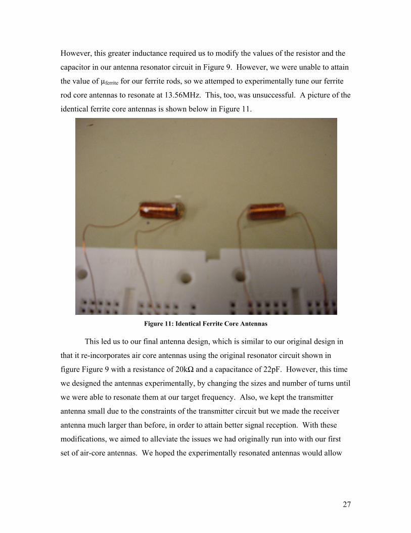
However, this greater inductance required us to modify the values of the resistor and the
capacitor in our antenna resonator circuit in Figure 9. However, we were unable to attain
the value of µferrite for our ferrite rods, so we attemped to experimentally tune our ferrite
rod core antennas to resonate at 13.56MHz. This, too, was unsuccessful. A picture of the
identical ferrite core antennas is shown below in Figure 11.
Figure 11: Identical Ferrite Core Antennas
This led us to our final antenna design, which is similar to our original design in
that it re-incorporates air core antennas using the original resonator circuit shown in
figure Figure 9 with a resistance of 20kΩ and a capacitance of 22pF. However, this time
we designed the antennas experimentally, by changing the sizes and number of turns until
we were able to resonate them at our target frequency. Also, we kept the transmitter
antenna small due to the constraints of the transmitter circuit but we made the receiver
antenna much larger than before, in order to attain better signal reception. With these
modifications, we aimed to alleviate the issues we had originally run into with our first
set of air-core antennas. We hoped the experimentally resonated antennas would allow

28
our setup to resonate at 13.56MHz and that the larger receiver antenna would be able to
pick up the signal with a stronger amplitude at the target frequency due to the resonance.
We were able to resonate the air-core transmitter antenna at ~13.56MHz with an inner
loop diameter of 8mm, an outer loop diameter of 13mm, and 22 turns. The transmitter
antenna is shown on the left of Figure 12 below.
Figure 12: Final Air Core Antennas
Completed Transmitter Stage Below is a picture of the completed transmitter stage.

29
Figure 13: Transmitter Stage
Receiver Side
Antenna & Filter – Receiver Side The first two receiver antennas were detailed in the antenna description for the
transmitter side, since the antennas were built to be identical. The final receiver stage
open-core small loop antenna that we ended up using, however, is different from the
transmitter side. We experimentally built this antenna, tuning it until it resonated at
13.56MHz with the circuit shown in Figure 14 below.
Figure 14: Receiver Antenna Resonator Circuit
The resistance and capacitance are the same as for the transmitter antenna resonator
circuit, 20kΩ and 22pF respectively. The antenna ended up having an inner diameter of
80mm, an outer diameter of 82mm, with 5 turns. The antenna also functions as a high-Q

30
band-pass filter centered at the resonant frequency of 13.56MHz. This eliminates the
need for a separate band-pass filter stage on the receiver side. However, before we were
able to obtain a steadily resonated antenna for the receiver stage, we built a high-Q band-
pass filter out of an op-amp, shown below in Figure 15.
Figure 15: High-Q Band-pass Filter (Source: Swarthmore.edu)
We chose 10pF for the capacitances and 33kΩ, 22Ω, and 62kΩ for R1, R2, and R3
respectively, in order to get a center frequency of 13.63MHz, a bandwidth of 513.4kHz,
and maximum gain of 0.9394 (to minimize attenuation through the filter), as detailed in
Equation 10 through Equation 12 below. Equation 10: Band-pass Filter Cutoff
12 ||
12 10pF 33 Ω||22Ω 62 Ω
13.63
Equation 11: Band-pass Filter Bandwidth 1 1
10pF 62 Ω 513.4
Equation 12: Band-pass Filter Amplification
262 Ω
2 33 Ω 0.9394
This design of band-pass filter ended up functioning well for our prototype, which we
had set to filter around a test frequency of 10kHz on a breadboard. However, when we
soldered our band-pass setup discussed above, we found that the filter did not function
well at the desired frequency of 13.56MHz due to the excessively low resistance and

31
capacitance values for R2 and C, and instead we opted to just rely on the innate high-Q
band-pass filter present in our tuned receiver antenna.
Amplification Stage
The received signal needs to be amplified before it can be demodulated and the
data can be decoded. We used 2 identical copies of the standard non-inverting amplifier
setup in series for our amplification stage. The schematic of a single setup and its gain is
shown in Figure 16 and Equation 13 below.
Figure 16: Receiving Stage Non-Inverting Amplifier
Equation 13: Gain of Receiving Stage Non-Inverting Amplifier
1 11 Ω
330Ω 4.03
Therefore, each amplifier should give a gain of approximately 4, for a total gain of
approximately 16 through our series amplifier stage. We chose to use two amplifiers in
series instead of pushing a single amplifier’s gain higher because lowering the gain of
each individual stage allowed the amplifiers to operate in higher frequency regions, due
to the principle of gain bandwidth product (GBP).
The operational amplifiers that we ordered were specifically fast with high GBPs
and high slew rates because we originally intended for them to amplify a signal switching
from rail to rail at our carrier frequency of 13.50MHz. However, the effective slew rate
requirement of our amplifiers is slightly lower because the signal will not be amplified to
the rails. The required slew rate for the op-amp is a function of our maximum switching
frequency, 13.50MHz, and the voltage potential that the op-amp will actually be
switching over. Since we are operating on signals between ground and 5V, this requires
a slew rate of at least 5 13.50 2 135 /μ . The LT1223’s have an input

32
slew rate of 350V/µs and a peak output slew rate of 2000V/µs, which is clearly sufficient
for our application.
Another requirement which we took into consideration when ordering our op-
amps was the speed of the envelope detector, which is the stage following the
amplification stage. This is because the signal coming out of the amplifier needs to be
switching at least as fast as the envelope detector can switch, otherwise data would be
lost in the demodulation. The time constant of the envelope detector is 220ns. This
means our minimum switching frequency needed to be 2.27 , which our
op-amps cover since they have a GBP of 100MHz.
Since our op-amps, the LT1223s, have a GBP of 100MHz, this should allow a
theoretical maximum amplification of .
7.41. However, due to second order
effects and imperfections in the op-amps themselves, we discovered that the theoretical
GBP of 100MHz was not truly attainable with gains above unity, so we lowered our
effective use of the available GBP by splitting our amplification across two identical
stages of lower amplification in order to have a higher quality of reliable amplification at
our target frequency. The input and output of our two-stage amplifier setup is shown
below in Figure 17. We can see that the obtained amplification in our target frequency
range is approximately ..
8.5, which is an amplification of approximately 3
through each stage of the amplifier. This is reasonable given the imperfections of the op-
amp and the high frequencies which we are amplifying.

33
Figure 17: Output vs Input of Amplifier
Demodulation – Envelope Detection An envelope detector is used to demodulate the signal. The schematic of the
envelope detector is shown below in Figure 18.
Figure 18: Envelope Detector Schematic
The diode that we used was a general purpose 1N914 diode. The values of the resistor
and capacitor were chosen in order to minimize the time constant τ, while adhering to the
constraint in Equation 14 below. Equation 14: Envelope Detector Constraint
1τ
1

34
This is because minimizing τ minimizes the negative peak clipping, effectively
improving the response of our demodulator. Increasing τ minimizes the ripple, however
since we are demodulating a digital signal, ripple is a much smaller concern than negative
peak clipping. Since fmodulation is 106kHz and fcarrier is 13.50MHz, we obtain the following
constraint on our values of R and C:
9.434μ 74.07
Our chosen values of R and C give us a τ of 220ns, which is ~4x larger than the lower
constraint of 74.07ns and ~50x smaller than the higher constraint of 9.434µs. These
values and the circuit functioned properly for the expected 106kHz modulation clock.
Clock Recovery – The Phase-Locked Loop In order to recover the data from the demodulated signal, we need to XOR the
demodulated signal with a square wave running at the clock frequency that was used to
encode the signal. In order to determine that clock frequency, an analog clock recovery
mechanism is implemented using a phase-locked loop (PLL). A high level diagram of
the PLL implementation is shown in Figure 19 below.
Figure 19: High Level PLL
The demodulated signal is fed into a phase comparator, which is an XOR. The
other input of the phase comparator is the output of the voltage-controlled oscillator
(VCO) fed backwards for negative feedback. The output of the phase comparator is sent
into a low-pass filter. The output of this low-pass filter is then fed into the VCO, whose
output is both the output of the PLL and is also fed back into the phase comparator for
negative feedback. Figure 20 below shows our specific implementation of the CD4046b
PLL.

35
Figure 20: CD4046B PLL (Source: Datasheet by Texas Instruments)
The values of R1, R2, R3, C1 and C2 were all chosen by approximating data points for
values of f0 and fmin from log-log curves in the datasheet of the PLL IC and using them in
conjunction with the following provided equations: Equation 15: fmax
Equation 16: fmin
Equation 17: fL
Equation 18: fc
12
2τ
Equation 19: τ τ R C
However, since the data points that were used to approximate f0 and fmin were at
best approximations, we noticed a considerable phase lag of up to 45˚ when we
implemented our calculated configuration. Therefore, we ended up using the calculated
resistor and capacitor values as only a starting point, and experimentally tweaked the
values until we were able to lock the PLL onto our sample 106kHz square wave with
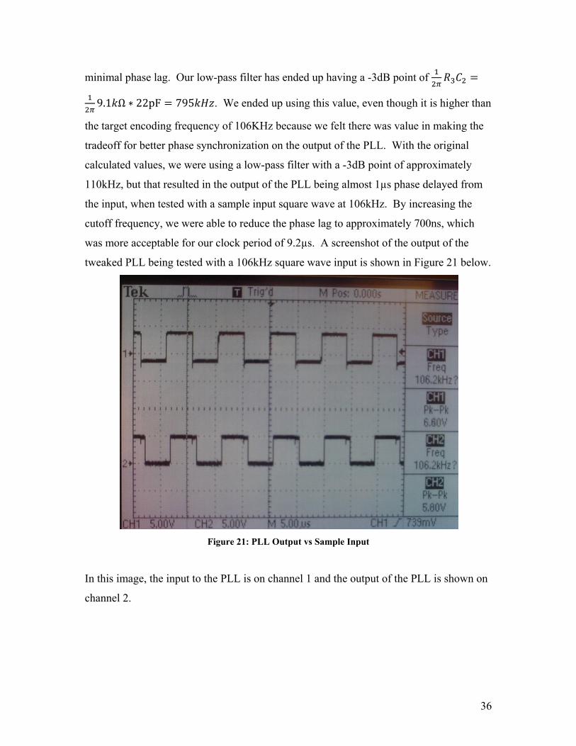
36
minimal phase lag. Our low-pass filter has ended up having a -3dB point of
9.1 Ω 22pF 795 . We ended up using this value, even though it is higher than
the target encoding frequency of 106KHz because we felt there was value in making the
tradeoff for better phase synchronization on the output of the PLL. With the original
calculated values, we were using a low-pass filter with a -3dB point of approximately
110kHz, but that resulted in the output of the PLL being almost 1µs phase delayed from
the input, when tested with a sample input square wave at 106kHz. By increasing the
cutoff frequency, we were able to reduce the phase lag to approximately 700ns, which
was more acceptable for our clock period of 9.2µs. A screenshot of the output of the
tweaked PLL being tested with a 106kHz square wave input is shown in Figure 21 below.
Figure 21: PLL Output vs Sample Input
In this image, the input to the PLL is on channel 1 and the output of the PLL is shown on
channel 2.

37
Decoding
Once the demodulated signal has its clock recovered by the PLL, decoding the
data from the signal is quite simple. The recovered clock from the PLL and the
demodulated signal are XOR’d by an XOR with a maximum propagation delay of 350ns,
and the original data signal is the output of the XOR. Since our original data signal is an
animal’s pulse, it will rarely be greater than 100Hz, which has a period of 0.01s.
Therefore, our XOR is sufficiently fast enough for decoding the data signal.
Mega32 Microcontroller – ADC & Serial Communication The Atmel Mega32 MCU is soldered onto a prototype board designed by Bruce
Land. Bruce was kind enough to donate a Rev7 board to us, which made the hardware
implementation of the Mega32 fast and painless. The webpage detailing the design of the
board and the hardware setup required is included in the References.
The Mega32 reads in the voltage value from the decoder on ADC0 which is set to
PINA.0 and converts it to a digital value. The 8 most significant bits in the ADCH
register are then printed out to the serial port at 9600 baud after each ADC conversion.
The serial code was leveraged from Bruce Land’s example code on serial
communication: interrupt driven serial communication. We implemented a delay of
20ms between each ADC conversion so that we don’t flood the serial port with data for
MATLAB. The Mega32 code is included in Appendix B.
Display – MATLAB The MATLAB script running on the PC opens a serial connection at 9600 baud
on whichever COM is available for the current PC. This COM port needs to be edited in
the script to reflect the port changes. Then the script goes into an infinite loop polling the
serial port for data. Data from serial is retrieved with a “scanf” command and then is left
shifted into a vector. Since the data from the ADC ranges from 0-255, it is first adjusted
to represent the voltage range by dividing by 255 and multiplying by 5. The vector is
then plotted using the “set” command so the plot updates with new points in real time.
Frequency is calculated by counting how many times the peaks in the vector are greater

38
than a threshold voltage of 2.5. That number is then divided by the size of the vector and
multiplied by a calibration constant to get the frequency. The calibration constant is set
so that the frequency calculation matches up with the given input frequency. This
frequency value is also constantly updated in the plot of the pulse. The MATLAB code
is included in Appendix C.
Completed Receiver Stage Below is a picture of the completed receiver stage.
Figure 22: Completed Receiver Stage

39
Results
All of the lower level components to our project worked to specification as
detailed in the Design and Implementation section of the report. However, upon combing
the pieces together and chaining outputs and inputs, we ran into considerable difficulties
with sub-circuit performance and behavior.
Though the PLL worked with the test signal from a signal generator, it wasn’t
able to lock in phase onto a real demodulated signal from the antenna. This shift in phase
is a skew between the clock and the data, and therefore the XOR that is decoding the
encoded signal suffers from devastating jitter when the signal should be a clean “high” or
“low” value. After considerable debugging and attempting to use different phase
comparators on the PLL IC, we decided to remove the encoding and decoding stages
from the transmit and receive stages in order to salvage the functional parts of the project.
However, removing the encoding and decoding stages had considerable impact on other
parts of the project which had already been designed and tested with encoding and
decoding in mind.
The ATTiny’s code was modified in order to remove the digital encoding that was
being performed. Now, the ATTiny functioned simply as a digital Schmidt trigger,
reading the input data into the ADC and outputting a digitized version of it onto the port
pin. The ATTiny still provides power management for the transmitter circuit through the
use of its power-down mode and its watchdog timer.
The envelope detector had to be changed due to the removal of signal decoding,
because the effective modulation frequency was changed from 106kHz to a few Hertz,
which is the frequency of the data. With this new modulation frequency, our old
envelope detector no longer worked, as the ripple was too large. The new modulation
frequency caused the constraint on RC to change to:
0.33 74.07
However, we found that following this constraint did not yield a difference in the output
of the envelope detector versus its input for an input signal of such a low frequency.
Therefore, the capacitor was changed from 22pF to 11pF, and the resistor was changed
from 10kΩ to 75Ω, yielding a new τ of 0.825ns, which is below the lower bound of the

40
constraint on τ. We kept this regardless because we found that increasing τ caused far too
much ripple in the output signal. The following figure shows the output of our envelope
detector with a sample modulated signal. As we expect, there is considerable ripple but
very little negative peak clipping.
Figure 23: Output vs Input of Modified Envelope Detector
The end result of all these simplifications to our circuit was that we are able to
read in an input through the EKG, amplify it and send it to the transmitter-stage MCU to
be digitized. Then it is modulated with our carrier wave at the NFC specifications and
transmitted over a small loop antenna to the receiver stage. This happens in bursts
interlaced with periods of powered-down modes so as to not drain the battery. The
receiver stage then amplifies the signal it receives and demodulates it before reading it
into the ADC of the receiver-stage MCU, the Mega32. The Mega32 then sends this data
via a serial connection to a MATLAB script running on a PC, which plots the data in
real-time and calculates the frequency and the beats-per-minute (BPM) of the signal for
the user to see. We did not attain our goal of encoding the data using the Manchester
encoding scheme due to problems retrieving the clock rate of the data from the PLL on

41
the receiving end. Other than this NPC specification-related issue, we managed to
perform all of the tasks that we had set out to accomplish.
The performance of our project was reasonably accurate, given that it is not an
actual medical device. The accuracy on the transmitter stage is highly dependent upon
the quality of the electrodes used. Since we are using high quality electrodes for our
input, our transmitter stage’s response is quite accurate. We noticed that given an input
of approximately 1Hz on the electrodes, the output of the input amplifier shows a
waveform with approximately 1 second period. A sample EKG is shown below in Figure
24.
Figure 24: Sample EKG from Zi Ling
This signal is then digitized and modulated successfully before being transmitted. A
picture of a sample EKG on channel 1 versus the modulated waveform on channel 2 is
shown below in Figure 25.

42
Figure 25: Sample EKG versus Modulated Signal from Hemanshu
The received signal on the receiver stage is representative of the transmitted
signal, except much lower in amplitude. Once demodulated, the signal is still
representative of the input. The actual waveform was destroyed when the signal was
digitized, so only the frequency data is recovered. This is then read into the Mega32 and
transmitted to the PC, which displays this digitized signal on a MATLAB plot.
Throughout this process, the frequency data is quite close to the input frequency.
However, the frequency and beats-per-minute calculation of the MATLAB plot may
sometimes be inaccurate due to non-precise calibration. A sample MATLAB plot is
shown below in Figure 26.

43
Figure 26: Sample MATLAB Plot
The input signal that generated this plot was approximately 2Hz, so we can see that the
MATLAB frequency calculation is slightly inaccurate. However, the waveform’s
frequency is visibly close to the input waveform’s frequency. We were unable to
calculate an exact percentage of difference due to the MATLAB waveform updating in
real time and lacking sophisticated measurement tools that the oscilloscope contains, so
instead we had to rely on visual confirmation of frequency resolution in the MATLAB
plot. Given these results, we are satisfied with our project’s performance.

44
Conclusion
We were fairly successful in accomplishing our goals. We successfully read in an
input signal from a living source and transmitted it wirelessly to a base station, which
then communicates with a PC and plots the information in a user-friendly format. The
shortcoming of our project is that we do not fully implement the NFC protocol since we
do not support a Manchester encoding scheme.
This project allowed us to significantly apply our computer engineering
knowledge while stretching our analog electrical engineering knowledge to its limits.
Looking back on our difficulty in using the PLL and getting it to output a clock signal in
phase, we should have allocated much more time to the PLL than we had allotted. Had
we been able to get the PLL working, our project would have fulfilled all of the goals it
had originally set out to accomplish. Other than the PLL, we feel that the rest of the
project was approached in a manner which allowed for efficient identification and solving
of problematic issues and we have no serious regrets. We feel that we learned a lot about
the details of designing working circuit components and integrating them together, which
is valuable design experience for engineers.

45
Acknowledgements
This project would not have been possible without the help and guidance of a few
key people. We first and foremost would like to thank Professor Bruce Land for all of his
help, insight, patience, and understanding throughout the project. We would also like to
thank Maxim IC for their kind donation of the MAX233 level shifters.
Hemanshu would like to thank his roommate and fellow Cornell ECE student,
Ankur Kumar, for his help with analog issues and MATLAB code. He would like to
thank his parents for all their guidance and support that made everything possible.
Zi Ling would like to thank Digikey for their fast, accurate, and costly shipping.
He would also like to thank his parents for the upbringing that made him what he is
today.

46
References
Knowledge Articles Microchip. “Antenna Circuit Design for RFID Applications.” http://ww1.microchip.com/downloads/en/AppNotes/00710c.pdf Sheshidher Nyalamadugu, Naveen Soodini, Madhurima Maddela, Subramanian Nambi and Stuart M. Wentworth. “Radio Frequency Identification Sensors.” http://cee.citadel.edu/asee-se/proceedings/ASEE2004/P2004132electNYA.pdf Barry Hanson. “Barry’s Inductor Simulation.” http://www.coilgun.info/mark2/inductorsim.htm P-N Designs. “Inductor mathematics.” http://www.microwaves101.com/encyclopedia/inductormath.cfm Jim Lesurf. “Loops and rods.” http://www.st-andrews.ac.uk/~www_pa/Scots_Guide/RadCom/part7/page5.html Jim Lesurf. “The Envelope Detector.” http://www.st-andrews.ac.uk/~www_pa/Scots_Guide/RadCom/part9/page2.html Erik Cheever. “Frequency Response and Active Filters.” http://www.swarthmore.edu/NatSci/echeeve1/Ref/FilterBkgrnd/Filters.html Wikipedia. “Near Field Communction.” http://en.wikipedia.org/wiki/Near_Field_Communication Wikipedia. “Manchester Code.” http://en.wikipedia.org/wiki/Manchester_code Bruce Land. “Microcontroller Board.” http://www.nbb.cornell.edu/neurobio/land/PROJECTS/Protoboard476/index.html Bruce Land. “Serial Communication.” http://instruct1.cit.cornell.edu/courses/ee476/Serialcom/SerialInt.c
Datasheets National Semiconductor. Voltage Buffer LM833 http://www.national.com/ds/LM/LM833.pdf Texas Instruments. Differential Amplifier INA121 http://focus.ti.com/lit/ds/symlink/ina121.pdf

47
Atmel. AVR MCU 2K 20MHZ ATTINY25-20PU http://www.atmel.com/dyn/resources/prod_documents/2586S.pdf Infineon. Low Side Switch BUZ73N http://www.infineon.com/dgdl/Buz73_Rev+2.2.pdf?folderId=db3a304412b407950112b408e8c90004&fileId=db3a304412b407950112b42b314b4492 Citizen Crystal and Oscillators. Oscillator 13.5 MHz CMX309FLC13 http://media.digikey.com/pdf/Data%20Sheets/Citizen%20PDFs/CMX-309.pdf Toshiba. NAND Quad 2INP TC74AC00P http://www.toshiba.com/taec/components2/Datasheet_Sync//149/83.pdf Linear Technology. Current Feedback Amp 100MHz LT1223CN8 http://www.linear.com/pc/downloadDocument.do?navId=H0,C1,C1154,C1009,C1146,P1473,D2786 Texas Instruments. Phase-Lock Loop MCPWR CD4046BE http://focus.ti.com/lit/ds/symlink/cd4046b.pdf ON Semiconductor. XOR MC14070BCPGOS http://www.onsemi.com/pub_link/Collateral/MC14070B-D.PDF Atmel. AVR MCU 32K ATMEGA324P-20PU http://www.atmel.com/dyn/resources/prod_documents/doc8011.pdf Maxim. RS232 Level Shifter MAX232 http://datasheets.maxim-ic.com/en/ds/MAX220-MAX249.pdf Fairchild Semiconductor. Diode 1N914 http://www.fairchildsemi.com/ds/1N/1N914B.pdf Atmel. Program Board STK500 http://www.atmel.com/dyn/resources/prod_documents/doc1925.pdf

48
Appendix A: Atmel ATTiny25 Code //ATtiny25 code //Reads in voltage values on PB2 and converts A to D //Outputs thresholded signal on PB1 and Manchester encoded signal on PB3 //Watchdog timer for power down mode with power down control signal to other ICs on PB4 //106 kHz CLK on PB0 for testing purposes //Zi Ling Kang (zk29) //Hemanshu Chawda (hkc2) //----------------INCLUDEs------------------------ #include <tiny25.h> #include <stdlib.h> #include <delay.h> #include <sleep.h> //----------------GLOBAL-VARIABLES------------------ int khz_count = 0; // Timer counter unsigned char count = 0x00; // Timer counter unsigned char sec_counter = 0x00; // LED 3 and 4 are switched // need to generate a sine wave at 4.068 MHz // http://instruct1.cit.cornell.edu/courses/ee476/labs/s2007/lab2.html unsigned char adcval = 0x00; unsigned char adcthres = 0x00; unsigned char adcmax = 0x00; unsigned char adcmin = 0xff; unsigned char clk106k = 0x0; // -----------------ISRs------------------------------------------ interrupt [TIM0_COMPA] void timer0_compareA() //find min and set threshold if (adcval < adcmin) adcmin = adcval; adcthres = (adcmax-adcmin)>>1; //find max and set threshold if (adcval > adcmax) adcmax = adcval; adcthres = (adcmax-adcmin)>>1; //toggle PB3 based on ADC value and threshold if (adcval <= adcthres) PORTB.1 = 0x0; PORTB.3 = clk106k; else PORTB.1 = 0x1; PORTB.3 = ~clk106k; PORTB.0 = ~PORTB.0; clk106k = ~clk106k; // This interrupt service routine is called when timer 0 overflows.

49
// Since prescalar is chosen to be 1, timer compares at frequency of 16MHz/(1 prescalar * 77 compare value) = 212.779kHz if(khz_count == 1023) // if khz_count has counted another khz, check to see if count has reached 212 khz_count = 0; if(count == 212) // if count has counted to 212, increment the second counter count = 0; sec_counter++; // toggle the LEDs hopefully every second else count++; // if khz_count has counted another khz but count isnt 212, increment count else khz_count++; // if khz_count hasn't reached 1023, just increment khz_count interrupt [WDT] void watchdog_timeout() // This interrupt service routine is called when the Watchdog Timer Timeouts // -----------MAIN-------------------------------------------------- int main() // set port B: Output - PB0, PB1; Input - PB2-PB5 DDRB = 0b111011; TCNT0 = 0; // clear timer counter TCCR0A = 0b00000010; TCCR0B = 0b00000001; // prescalar = 1 (full clock rate) OCR0A = 76; // compare value of 76 for timer 0 compare -> generate 106kHz square wave // since 0 indexed, divide 16MHz/77 -> 212khz switching -> 106kHz square wave TIMSK = 0b00010000; // enable timer0a compare match interrupt // ADC ADMUX = 0b00100001; // Vcc used as Vref-, right adjusted, MUX = 0001 to select PB2 ADCSRA = 0b11000101; // Enable ADC, start first conversion, and set prescalar to 16 // Wait for conversion to complete while( ADCSRA.6 == 0b1) // Power Reduction Register PRR = 0b00001010; // Turn off the timer1 and USI (universal serial interface) to save power // MCU Control Register MCUCR = 0b10110100; // diable BOD during sleep and enable sleep to go into power-down mode // Watchdog Timer Control Register

50
WDTCR = 0b01111001; // Watchdog Timeout Interrupt Enable and Change Enable and Watchdog Enable // set to timeout every 1024k cycles at 128kHz = 8 seconds but for some reason goes 16 seconds... PORTB.4 = 0x0; // enable interrupts #asm("sei"); sleep_enable(); while (1) PORTB.4 = 0x1; //power down signal high when not in power down mode // Start the conversion ADCSRA.6 = 0b1; // Wait for conversion to complete while( ADCSRA.6 == 0b1) adcval = ADCH; //get the 8 MSBs of the ADC /* //find min and set threshold if (adcval < adcmin) adcmin = adcval; adcthres = (adcmax-adcmin)>>1; //find max and set threshold if (adcval > adcmax) adcmax = adcval; adcthres = (adcmax-adcmin)>>1; //toggle PB1 based on ADC value and threshold, Manchester encoding on PB3 if (adcval <= adcthres) PORTB.1 = 0x0; PORTB.3 = clk106k; else PORTB.1 = 0x1; PORTB.3 = ~clk106k; */ //reset values and power down if (sec_counter == 8) adcmax = 0x00; adcmin = 0xff; PORTB.1 = 0x0; PORTB.3 = 0x0; PORTB.4 = 0x0; //power down signal powerdown(); //power down ATtiny25 to save power return 0; // never happens but gets rid of warning!

51
Appendix B: Atmel Mega32 Code // Hemanshu Chawda (hkc2) // Zi Ling Kang (zk29) // Atmel Mega32 code (taken largely from Bruce Land's example serial code) #include <mega32.h> #include <stdio.h> #include <delay.h> //timeout values for each task #define t1 100 #define t2 1000 //the subroutines void task1(void); //test for button press void task2(void); //increment note to be played void gets_int(void); //starts getting a string from serial line void puts_int(void); //starts a send to serial line void initialize(void); //all the usual mcu stuff unsigned int time1, time2 ; //task scheduling timeout counters unsigned long time; unsigned int v; //RXC ISR variables unsigned char r_index; //current string index unsigned char r_buffer[16]; //input string unsigned char r_ready; //flag for receive done unsigned char r_char; //current character //TX empth ISR variables unsigned char t_index; //current string index unsigned char t_buffer[16]; //output string unsigned char t_ready; //flag for transmit done unsigned char t_char; //current character //********************************************************** //timer 0 compare-match ISR, every 1 msec interrupt [TIM0_COMP] void timer0_overflow(void) time++; //Decrement the three times if they are not already zero if (time1>0) --time1; if (time2>0) --time2; //********************************************************** //UART character-ready ISR interrupt [USART_RXC] void uart_rec(void) r_char=UDR; //get a char UDR=r_char; //then print it //build the input string if (r_char != '\r') r_buffer[r_index++]=r_char;

52
else putchar('\n'); //use putchar to avoid overwrite r_buffer[r_index]=0x00; //zero terminate r_ready=1; //signal cmd processor UCSRB.7=0; //stop rec ISR /**********************************************************/ //UART xmit-empty ISR interrupt [USART_DRE] void uart_send(void) t_char = t_buffer[++t_index]; if (t_char == 0) UCSRB.5=0; //kill isr t_ready=1; //transmit done else UDR = t_char ; //send the char /**********************************************************/ //********************************************************** //Entry point and task scheduler loop void main(void) initialize(); //main task scheduler loop -- never exits! while(1) ADCSRA.6 = 0x1; //start the conversion while (ADCSRA.6 == 0x1) //wait until conversion finishes printf("%d\r\n", ADCH); //print ADC value to serial puts_int(); delay_ms(20); //get next ADC conversion after 20 ms for timing issues if (time1==0) task1(); // if (time2==0) task2(); //********************************************************** //Task 1 input a string and print it void task1(void) time1=t1; //reset the task timer //print and get another serial string if (r_ready ) //sscanf(r_buffer,"%d",&v); //gets_int();

53
//********************************************************** //Task 2 print the system time void task2(void) time2=t2; //reset the task timer //sprintf(t_buffer,"%ld %d\n\r",time,v) ; puts_int(); //********************************************************** // -- non-blocking keyboard check initializes ISR-driven // receive. This routine merely sets up the ISR, which then //does all the work of getting a command. void gets_int(void) r_ready=0; r_index=0; UCSRB.7=1; // RX Complete Interrupt Enable //********************************************************** // -- nonblocking print: initializes ISR-driven // transmit. This routine merely sets up the ISR, then //send one character, The ISR does all the work. void puts_int(void) t_ready=0; t_index=0; if (t_buffer[0]>0) putchar(t_buffer[0]); UCSRB.5=1; // USART Data Register Empty Interrupt Enable //********************************************************** //Set it all up void initialize(void) //serial setop for debugging using printf, etc. UCSRB = 0x18 ; // Tx and Rx enable UBRRL = 103 ; // set baud rate to 9600 for single rate transmission and 16MHz crystal //set up timer 0 TCCR0=0b00001011; // prescalar to 64 and Clr-on-match OCR0=249; // 16MHz/64 prescalar * 250 counts -> set output compare register to 1 mSec TIMSK=2; // turn on timer 0 output compare-match interrupt //init the task timers time1=t1; time2=t2; r_ready=0;

54
t_ready=1; ADMUX = 0b01100000; //ref = AVCC, ADC0 ADCSRA = 0b11000111; //prescaler = 128 => ADC speed 16MHz/128 = 128 kHz ADCSRA.6 = 0x1; //do an ADC conversion to get out any bugs while (ADCSRA.6 == 0b0) //crank up the ISRs #asm sei #endasm gets_int();

55
Appendix C: MATLAB Script %=====clean up any leftover serial connections============== clear all try fclose(instrfind) %close any bogus serial connections end %=====open a serial connection=============================== %set its rate to 9600 baud %SR830 terminator character is (ACSII 13) %use fprintf(s,['m' mode]) to write %find which COM port you need!!!! s = serial('COM1','baudrate',9600,'terminator',13); fopen(s); disp('serial communication setup complete'); %defines and init values PLOT_SIZE = 200; CALIB_CONST = 20; vect = zeros(1, 200); figure(1); pulse = plot(vect); pulseTitle = title('Freq ~ BPM ~'); %infinite loop to continuously poll serial com and plot data while (1) vect = vect([ 2:end 1 ]); %left shift data vector temp = fscanf(s, '%d'); %get data from serial if (temp <= 255) %only use values that aren't bogus, ADC values range from 0-255 vect(PLOT_SIZE) = 5*temp/255; %adjust ADC value from 0-5V thres = (min(vect)+max(vect))/2; %calculate threshold counti = 0; for i=1:200 %count number of pulses that pass threshold in data vector if (i > 1) if (vect(i) >= thres && vect(i-1) <= thres) counti = counti + 1; end end end set(pulse, 'YData', vect); %update the plot with new data drawnow; pfreq = CALIB_CONST*counti/PLOT_SIZE; %get frequency from count/total size adjusted by constant pbpm = 60*pfreq; pTitle = sprintf('Freq ~ %5.2f Hz BPM ~ %d', pfreq, pbpm); %update frequency value and BPM value set(pulseTitle, 'String', pTitle); end end

56
Appendix D: Parts Cost List Part Name Unit
Cost Quantity Total
Cost Ferrite Rod FRD12875 $1.50 1 $1.50 Ferrite Rod FRD18750 $1.50 1 $1.50 Threaded Ferrite Rod FRD18375 $3.00 1 $3.00 Switch Reed SPST 1A 22‐388 A/T HE505 $1.30 1 $1.30 Switch Reed SPST .5A 12‐33 A/T HE503 $0.72 1 $0.72 Switch Reed SPST .5A 22‐33 A/T HE504 $2.34 1 $2.34 Socket Adapter SOIC/8PIN .300 DIP A724 $5.96 2 $11.92 PLL CLK Mult PI6C4511WE $1.37 3 $4.11 AVR MCU 2K 20MHZ ATTINY25‐20PU $1.76 6 $10.56 AVR MCU 32K ATMEGA324P‐20PU $6.02 1 $6.02 Oscillator 13.5 MHz 300‐7027‐1 $3.00 4 $12.00 NAND Dual 2INP 497‐1343‐5 $0.50 2 $1.00 XOR MC14070BCPGOS $0.68 4 $2.72 OP Amp Dual Audio LM833NNS $0.94 3 $2.82 OP Amp High Slew Rate LM318N $1.40 5 $7.00 Current Feedback Amp 100MHz LT1223CN8
$5.38 5 $26.90
Mod/Demod Balanced MC1496PGOS $1.12 3 $3.36 Mod/Demod Double Balanced NJM1496M $1.65 2 $3.30 Phase‐Lock Loop MCPWR 296‐2052‐5 $0.56 2 $1.12 PLL W/VCO/Lock Detect 296‐9237‐5 $1.93 2 $3.86 NAND Quad 2INP TC74AC00P $0.46 2 $0.92 6V Lithium Battery $5.00 4 $20.00 RS232 Level Shifter MAX232 $2.40 1 $2.40 Diff Amp INA121 $5.00 1 $5.00 Low Side Switch BUZ73N $1.27 1 $1.27 Diode 1N914 $0.01 1 $0.01 Resistors $0.00 50 $0.01 Capacitors $0.00 50 $0.01 Wires and Solder $0.00 100 $0.01 Solder Board $1.99 2 $3.98 EKG Electrodes $0.40 10 $4.00
Subtotal $134.75 Shipping & Handling $57.45 Sales Tax Paid $9.36
Total $201.56